

Page 1
PRELIMINARY
Intel® 82430NX Chipset
Level II Cache Module Family
CYM74BP54
CYM74P54/55
CYM74SP54/55
Cypress Semiconductor Corporation • 3901 North First Street • San Jose • CA 95134 • 408-943-2600
May 1994 – Revised October 1995
1CYM74S P54/55
Features
• Pin-compatible secondary cache module family
• Asynchronous (CYM74BP54), synchronous pipelined
(CYM74P54, CYM74P55), or synchronous
(CYM74SP54, CYM74SP55) configurations with presence and configuration detect pins
• Ideal for Intel® P54C-based systems with th e 82430 N X
(Neptune) chipset
• Operates at 60 and 66 MHz
• Uses cost-effective CMOS asynchronous SRAMs or
high-performance synchronous SRAMs
• 160-position Burndy DIMM CELP2X80SC3Z48
connector
• 3.3V inputs/outputs
Functional Descriptio n
This family of secondary cache modules is designed for Intel
P54C systems with the 82430NX (Neptune) chipset.
CYM74BP54 is an asynchronous 256-Kbyte cache module
that provides a low-cost, high-performance solution with in-
dustry standard 5V SRAMs and 3.3V level t ranslators for CPU
bus speeds up to 66 MHz. The CYM74BP54 is organized as
32K by 64-bits.
The synchronous modules are available with low-cost synchronous pipelined RAMs or h igher performance sync h ronous
burst RAMs. The synchronous pipelined modules are based
on a 16Kx64 RAM. The CYM74P54 is a 256-KB module while
the CYM74P55 is a 512-KB module. Both are modules without
byte parity.
The CYM74SP54 and CYM74SP55 are synchronous burst
cache modules that provide zero wait-state performance at a
bus speed of 66 MHz. The CYM74SP54 is a 256-Kby te cache
module with byte parity. The CYM74SP55 is a 512-Kbyte
cache module with byte parity.
Multiple ground pins and on-board decoupling capacitors ensure high performance with maximum noise immunity.
All components on the cache modules are surface mounted
on a multi-layer epoxy laminate (multifunctional) substrate.
The contact pins are plated with 150 micro-inches of nickel
covered by 10 micro-inches of gold flash.
Intel is a registered trademark of Intel Corporation.
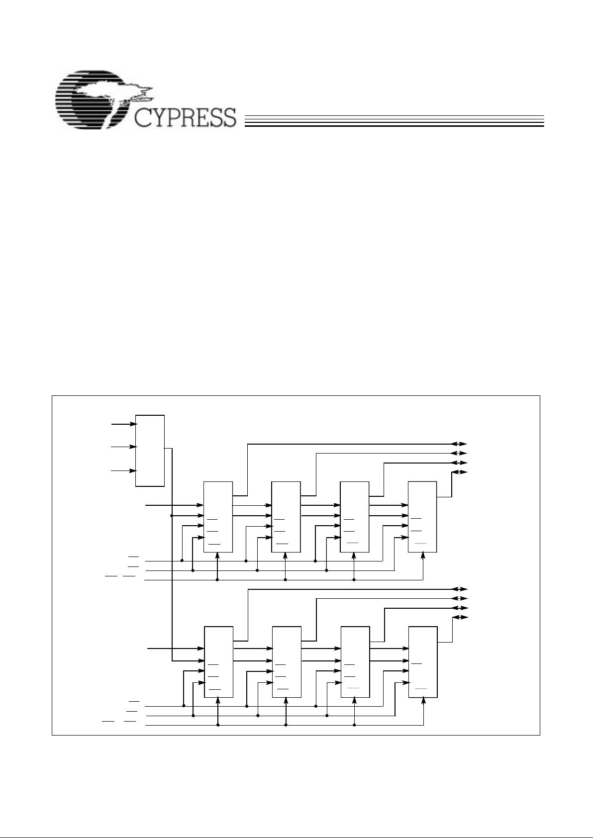
A
Logic Block Diagram -
CYM74BP54
LA17-LA
5
WE
0
WE
1
WE
2
WE
3
AAA
D
DD
D
CE
OE
CE
OE
CE
OE
CE
OE
WE
4
WE
5
WE
6
WE
7
AAAA
D
DD
D
CE
OE
CE
OE
CE
OE
CE
OE
CE
0
OE
0
WE0-WE
3
OE
1
WE4-WE
7
D0-D
7
D8-D
15
D16-D
23
D24-D
31
D32-D
39
D40-D
47
D48-D
55
D56-D
63
32K x 8
32K x 8
32K x 8 32K x 8
32K x 8
32K x 8 32K x 8 32K x
8
A
4–0-A3–0
A
4–1-A3–1
A17-A
7
ADDRESS LATCH
LE
CALE
A
74BP54–1
A
6–0-A5–0
CE
1
Page 2
CYM74BP54
CYM74P54/55
CYM74SP54/55
PRELIMINARY
2
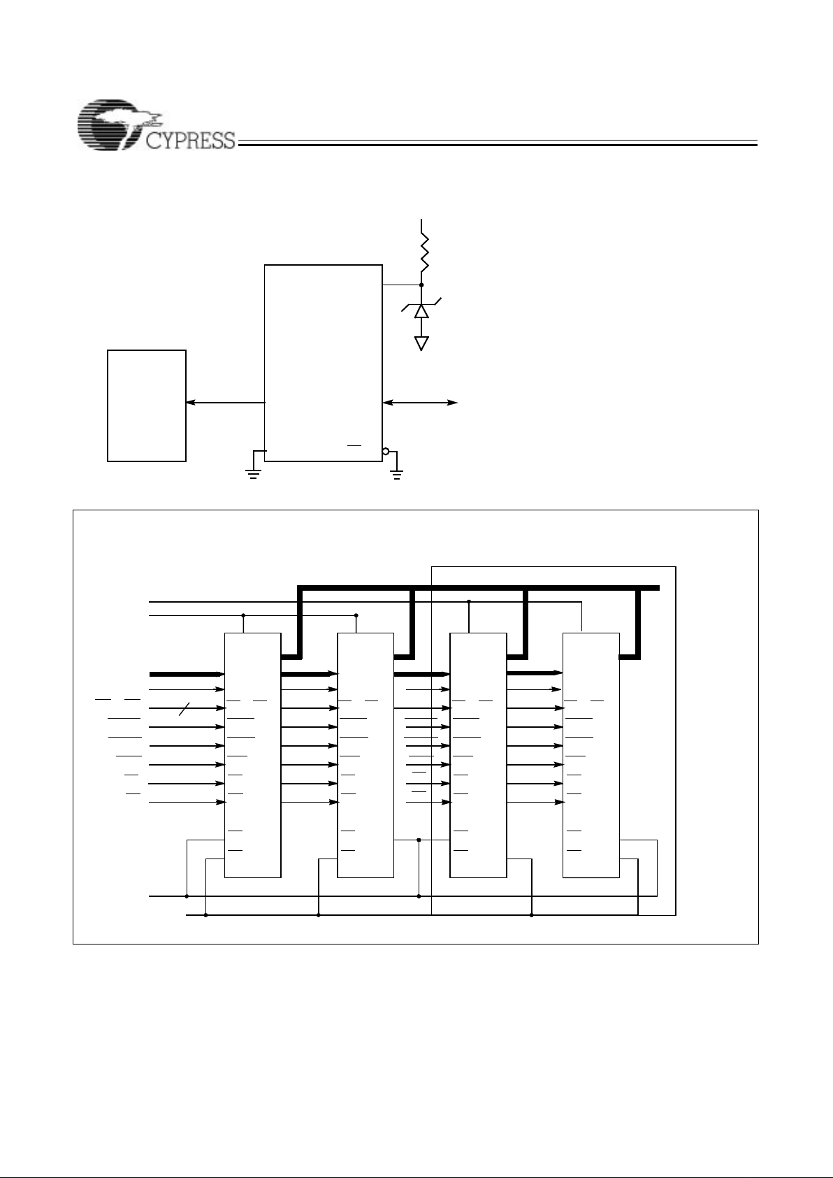
Block Diagram: 5V to 3.3V Level Conversion (CYM74BP54)
5VSRAM
64BitBusSwitch
5.0Volts
Vcc
(uses7CYBUS3384)
BE
[2:1]
B
D
3.3VcompliantI/O
GND
4.3Vzener
5%tolerance
100ohms
74BP54–2
D
CS
0
OE
CE
0
OE
0
WE7-WE
0
A
A16-A
7
ADV0 ADV
ADSC0 ADSC
ADSP
CLK0
8
BE0-BE
7
CK
A
17
CYM74P55 (A
18
)
CS
1
CS2CS
3
CS
4
V
CC
V
CC
D
CS
0
OE
A
ADV
ADSC
ADSP
CK
CS
1
CS2CS
3
CS
4
V
CC
D
CS
0
OE
A
ADV
ADSC
ADSP
BE0-BE
7
CK
CS
1
CS2CS
3
CS
4
V
CC
D
CS
0
OE
A
ADV
ADSC
ADSP
CK
CS
1
CS2CS
3
CS
4
D63-D
0
GND
GND
GND
GND
CYM74P55ONLY
16Kx64 16Kx64 16Kx64 16Kx64
CYM74P54(GND)
BE0-BE
7
BE0-BE
7
PD2PD1PD
0
CYM74P54
CYM74P55
ADSP0
TBD TBD TBD
TBD TBD TBD
ADV1
ADSC1
ADSP1
CE
1
OE
1
A
6–0-A3–
0
A
6–1-A3–
1
CLK1
74BP54–3
AAAA
Logic Block Diagram - CYM74P54, CYM74P55
Page 3
CYM74BP54
CYM74P54/55
CYM74SP54/55
PRELIMINARY
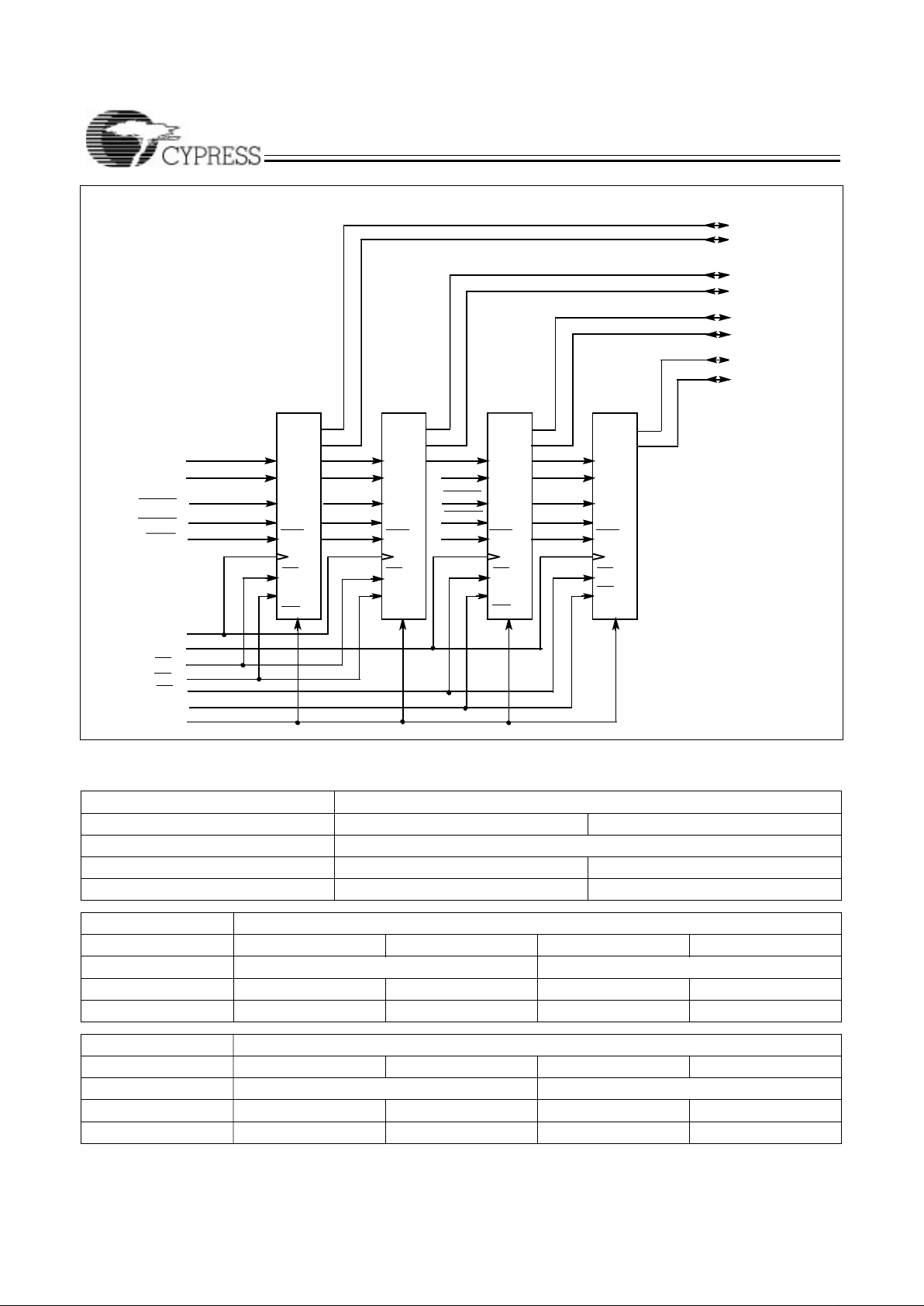
3
WE0/1
WE2/3
WE4/5
WE6/7
AAA
D
DD
D
CE
OE
CE
OE
CE
OE
CE
OE
CE
0
OE
0
WE0-WE
7
D0-D
15
D16-D
31
D32-D
47
D48-D
63
A
6–0-A3–0
A
A
18-A7
DP2-DP
3
DP0-DP
1
DP4-DP
5
DP6-DP
7
ADV0
ADV ADV ADV ADV
ADSC0
ADSC ADSC ADSC ADSCADSC ADSC ADSC ADSC
ADSP0
ADSP ADSP ADSP ADSP
CLK0
74BP54–4
(CYM74SP54)32Kx 18
(CYM74SP55)64Kx18
Note:A
18
isnotusedbyCYM74SP54
CLK1
CE
1
OE
1
ADSP1
ADSC1
ADV1
A
6–1-A3–1
Logic Block Diagram - CYM74SP54/CYM74SP55
Selection G uide
Asynchronous Cache Modules
Part Number CYM74BP54-60 CYM74BP54-66
Cache Size (KB) 256
System Clock (MHz) 60 66
RAM Speed tAA=15 ns tAA=12 ns
Synchronous Pipelined Cache Modules
Part Number CYM74P54-60 CYM74P54-66 CYM74P55-60 CYM74P55-66
Cache Size (KB) 256 512
System Clock (MHz) 60 66 60 66
RAM Speed t
CDV
=10.5 ns t
CDV
=8.5 ns t
CDV
=10.5 ns t
CDV
=8.5 ns
Synchornous Burst Cache Modules
Part Number CYM74SP54-60 CYM74SP54-66 CYM74SP55-60 CYM74SP55-66
Cache Size (KB) 256 512
System Clock (MHz) 60 66 60 66
RAM Speed t
CDV
=10.5 ns t
CDV
=8.5 ns t
CDV
=10.5 ns t
CDV
=8.5 ns
Page 4

CYM74BP54
CYM74P54/55
CYM74SP54/55
PRELIMINARY
4
Pin Configuration
74BP54–5
Top View
Dual Read–Out SIMM
(DIMM)
10
9
5
6
7
8
4
1
2
GND
D
63
GND
D
62
D
58
GND
NC (74BP54)/ DP
6
(74P5X, 74SP5X)
D
54
V
CC
D
61
V
CC
D
59
(74P5X, 74SP5X) DP7/ (74BP54)NC
D
55
D
57
GND
D
56
NC (74BP54) / V
CCQ
(74P5X, 74SP5X)
D
60
3
90
89
85
86
87
88
84
81
82
83
20
19
15
16
17
18
14
11
12
D
52
D
50
D
46
D
44
GND
D40
D
42
GND
D
48
13
30
29
25
26
27
28
24
21
22
D
38
D
36
D
32
D
30
D
26
D
24
GND
D
28
D
34
GND
23
39
35
36
37
38
34
31
32
D
22
D
18
GND
D
14
D
12
D
16
D
20
33
40
41
42
GND
D
10
52
51
47
48
49
50
46
43
44
D
8
D
6
D
4
D
0
GND
A
3–0
D
2
45
57
58
59
60
56
53
54
A
4–0
A
5–0
GND
A
10
A
14
A
12
A
8
55
69
65
66
67
68
64
61
62
A
16
NC (74BP54, 74SP54) / GND (74P54) / A18(74P55, 74SP55)
PD
2
NC (74BP54, 74P54) / CLK1 (74P55, 74SP5X)
GND
WE
6
WE
4
NC (Reserved CLK3)
GND
PD
0
63
70
79
75
76
77
78
74
71
72
WE
2
WE
0
CE
0
NC (74BP54) / ADV0(74P5X, 74SP5X)
NC (74BP54) /
ADSP0(74P5X, 74SP5X)
GND
OE
0
GND
73
80
D
53
D
51
GND
D
49
D
47
D
45
D
41
D
43
GND
100
99
95
96
97
98
94
91
92
93
D
39
D
37
D
35
GND
D
33
D
31
D
25
GND
D
29
D
27
110
109
105
106
107
108
104
101
102
103
(74P5X, 74SP5X) DP
3
/ (74BP54)NC
D
23
D
21
V
CC
D
19
GND
D
15
D
13
D
17
V
CC
120
119
115
116
117
118
114
111
112
113
GND
D
11
121
122
V
CC
D
9
(74P5X, 74SP5X) DP1/ (74BP54)NC
V
CC
D
7
D
5
D
3
D
1
127
128
129
130
126
123
124
125
GND
A
3–1
A
4–1
(74P5X, 74SP5X) A
5–1
/ (74BP54)NC
A
7
A
11
A
13
GND
A
9
140
139
135
136
137
138
134
131
132
133
A
15
A
17
GND
(ReservedA
19
)NC
PD1
(74P5X, 74SP5X)CLK0 / (74BP54) NC
WE
7
WE
5
(ReservedCLK2) NC
150
149
145
146
147
148
144
141
142
143
WE
3
WE
1
GND
(74P55, 74SP5X)
ADSC1 / (74BP54, 74P54) NC
(74P55, 74SP5X) ADV1 / (74BP54, 74P54) NC
(74P55, 74SP5X)
ADSP1/ (74BP54, 74P54) NC
GND
OE
1
V
CC
160
159
155
156
157
158
154
151
152
153
(74P5X, 74SP5X) DP
5
/ (74BP54)NC
GND
CALE (74BP54) /
ADSC0 (74P5X, 74SP5X)
NC (74BP54) / DP
4
(74P5X, 74SP5X)
NC (74BP54) / DP
2
(74P5X, 74SP5X)
NC (74BP54) / DP
0
(74P5X, 74SP5X)
CE
1
NC (74BP54) / V
CCQ
(74P5X, 74SP5X)
NC (74BP54) / V
CCQ
(74P5X, 74SP5X)
NC (74BP54) / V
CCQ
(74P5X, 74SP5X)
NC (74BP54) / V
CCQ
(74P5X, 74SP5X)
NC (74BP54) / V
CCQ
(74P5X, 74SP5X)
NC (74BP54) / V
CCQ
(74P5X, 74SP5X)
A
6–0
(74P5X, 74SP5X) A
6–1
/ (74BP54)NC
Page 5

CYM74BP54
CYM74P54/55
CYM74SP54/55
PRELIMINARY
5
Pin Definitions
Common Signals Description
V
CC
5V Supply
GND Ground
A7–A
19
Addresses from processor
A
3–0
, A
4–0
Lower address from chipset, identical to the bank1 addresses
A
3–1
, A
4–1
Lower address from chipset, identical to the bank0 addresses, A
3-1
, A
4-1
not used on
CYM74P54
A
5–0
, A
6–0
Lower address from processor (CYM74P5X, CYM74SP5X- identical to the bank1
addresses)
CE0, CE
1
Chip Enable (same signal), CE1 not used on CYM74P54
OE0, OE
1
Output Enable (same signal), OE1 not used on CYM74P54
WE0, WE1,WE2,WE
3
WE4,WE5,WE6,WE
7
Byte Write Enables
PD0–PD
2
Presence Detect pins
D0–D
63
Data lines from processor
NC Signal not connected on module.
CYM74BP54 Only Signals Description
CALE Latch Enable
CYM74P5X, CYM74SP5X Signals Description
V
CCQ
3.3V Supply
DP0–DP
7
Data Parity lines (Optional)
ADSP0, ADSP1 Processor Address Strobe, ADSP1 not used on CYM74P54
ADSC0,ADSC1 Cache Controller Address Strobe, ADSC1 not used on CYM74P54
ADV0, ADV1 Burst Address Advance, ADV1 not used on CYM74P54
A
5–1
, A
6–1
Lower address from processor , identical to the bank0 addresses, A
5-1
, A
6-1
not used on
CYM74P54
CLK0, CLK1, CLK2, CLK3 Clock signals (each should be given own clk driver); CLK0 used on CYM74P5X,
CYM74SP5X; CLK1 not used on CYM74P54; CLK2 and CLK3 are RSVD
Presence Detect Pins
PD
2
PD
1
PD
0
Asynchronous – CYM74BP54 NC GND NC
Synchronous Pipelined – CYM74P54 TBD TBD TBD
Synchronous Pipelined – CYM74P55 TBD TBD TBD
Synchronous Burst – CYM74SP54 GND GND NC
Synchronous Burst – CYM74SP55 GND GND GND
Page 6

CYM74BP54
CYM74P54/55
CYM74SP54/55
PRELIMINARY
6
Maximum Ratings
(Above which the useful life may be impaired. For user guidelines, not tested.
Storage Temperature................................. –55°C to +125°C
Ambient Temperature
with Power Applied.........................................–0°C to +70°C
3.3V Supply Voltage to Ground Potential.....–0.5V to +5.25V
5V Supply Voltage to Ground Potential........ –0.5V t o +5.25V
DC Voltage Applied to Outputs
in High Z State ............................................... –0.5V to +4.6V
DC Input Voltage............................................–0.5V to +4.6V
Output Current into Outputs (LOW)............................. 20 mA
Document #: 38-M-00070-B
Operating Range
Range
Ambient
Tempera-
ture
V
CC
V
CCQ
Commercial
(CYM74BP54)
0°C to
+70°C
5V ± 5% N/A
Commercial
(CYM74P5X,
CYM74SP5X)
0°C to
+70°C
5V ± 5% 5V ± 5%
3.3V + 10%
– 5%
Electrical Characteristics Over the Operating Range
Parameter Description Test Condition Min. Max. Unit
V
IH
Input HIGH Voltage 2.2 V
V
IL
Input LOW Voltage CYM74BP54 -0.5 0.8 V
V
IL
Input LOW Voltage CYM74P5X, CYM74SP5X -0.3 0.8 V
V
OH
Output HIGH Voltage VCC=Min. IOH = -4 mA 2.4 V
V
OL
Output LOW Voltage VCC=Min. IOL = 8 mA 0.4 V
I
CC (74BP54)
VCC Operating Supply Current VCC=Max., I
OUT
=0 mA, f=f
MAX
=1/t
RC
1700 mA
I
CC (74P54 )
VCC Operating Supply Current VCC=Max., I
OUT
=0 mA, f=f
MAX
=1/t
RC
TBD mA
I
CC (74P55 )
VCC Operating Supply Current VCC=Max., I
OUT
=0 mA, f=f
MAX
=1/t
RC
TBD mA
I
CC (74SP54)
VCC Operating Supply Current VCC=Max., I
OUT
=0 mA, f=f
MAX
=1/t
RC
1100 mA
I
CC (74SP55)
VCC Operating Supply Current VCC=Max., I
OUT
=0 mA, f=f
MAX
=1/t
RC
1400 mA
Ordering Info rma tio n
Speed
(MHz)
Ordering Code
Package
Name
Package Type Description
Operating
Range
60 CYM74BP54PM-60 PM36 160-Pin Dual-Readout SIMM Asynchronous 256KB Commercial
CYM74P54PM-60 TBD 160-Pin Dual-Readout SIMM Synch Pipelined 256KB
CYM74P55PM-60 TBD 160-Pin Dual-Readout SIMM Synch Pipelined 512KB
CYM74SP54PM-60 PM26 160-Pin Dual-Readout SIMM Synch Burst 256KB
CYM74SP55PM-60 PM26 160-Pin Dual-Readout SIMM Synch Burst 512KB
66 CYM74BP54PM-66 PM36 160-Pin Dual-Readout SIMM Asynchronous 256KB Commercial
CYM74P54PM-66 TBD 160-Pin Dual-Readout SIMM Synch Pipelined 256KB
CYM74P55PM-66 TBD 160-Pin Dual-Readout SIMM Synch Pipelined 512KB
CYM74SP54PM-66 PM26 160-Pin Dual-Readout SIMM Synch Burst 256KB
CYM74SP55PM-66 PM26 160-Pin Dual-Readout SIMM Synch Burst 512KB
Page 7

CYM74BP54
CYM74P54/55
CYM74SP54/55
PRELIMINARY
© Cypress Semiconductor Corporation, 1995. The information contained herein is subject to change without notice. Cypress Semiconductor Corporation assumes no responsibility for the use
of any circuitry othe r than circui try embodi ed in a Cypress Semi conductor p roduct. Nor does it convey or imply any licens e under patent or other rights. Cypress Semi conductor does not authori ze
its products for use as critical components in life-support systems where a malfunction or failure may reasonably be expected to result in significant injury to the user. The inclusion of Cypress
Semiconductor products in life-support systems application implies that the manufacturer assumes all risk of such use and in doing so indemnifies Cypress Semiconductor against all charges.
Package Diagrams
160-Pin Dual-Readout SIMM PM26
160-Pin Dual Readout SIMM PM36
 Loading...