

Page 1
1
www.clare.com
CYG2911
DS-CYG2911-R1
The CYG291 1 is a Data Access Arrangement (DAA) module providing a complete telephone line interface circuit in
a small 1.07" x 1.07" x 0.4" plastic package. This module
incorporates a circuit which signals HIGH when another
phone in parallel has been taken off-hook when the
CYG2911 is off-hook. This feature is important for cable
TV set-top boxes and direct broadcast satellite units
which must hang-up (go on-hook) when a consumer
needs the phone line to place a 911 or emergency call.
The module is designed to meet FCC Part 68 requirements thus providing a low-risk design solution.
• Home medical devices
• Plant monitoring equipment
• Security/alarm systems
• Utility meters
• Network routers
• PBX systems
• Telephony applications
• Set top boxes
• UL 1950/UL1459
• Compatible with U.S. and Canadian phone lines
• Transformer signal coupling
• Complete ring detector circuit
• Low power hookswitch
• Electronic inductor/gyrator circuit
• Surge protection
• Caller ID pinout to external relay (optional)
• Transient protection zeners
• V.32 compatible
• FCC Compatible
• PC board mountable
• Parallel telephone off-hook detection
Applications
Features
Description
Approvals
Cybergate™
Ordering Information
Part # Description
CYG2911 DAA Module
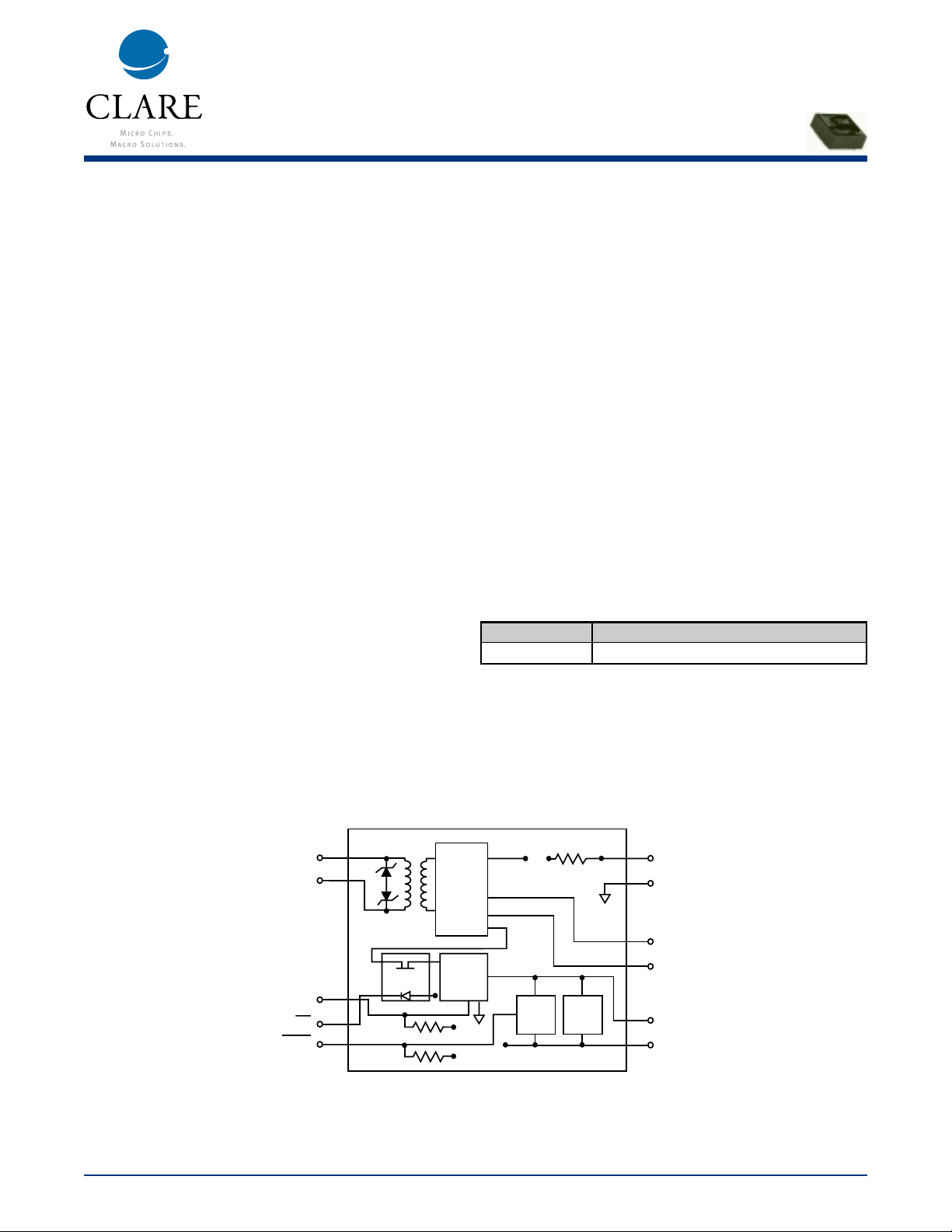
Block Diagram
8
7
9
RING
OH
911
1
2
17
18
11
10
14
13
HOOKSWITCH
LINE 2
LINE 1
RING
GND
V
CC
V
CC
TIP
RING
GYRATOR/
CALLER ID
V
CC
RING
R_LIM
R_LIM
V
CC
200k
47k
911
RING
DETEC-
TION
SURGE
PROTEC-
TION
CID1
CID2
CYG2911
470Ω
Handling and Assembly Recommendations
The CYG2911 products are not hermetically sealed and should not be exposed to any liquid-based rinsing processes. Clare recommends two (2) approaches. The modem
should either use a no clean soldering flux that would mostly evaporate during the normal wave soldering processes, or be soldered in by hand after the rest of the card
is wave soldered.
Page 2
www.clare.com
CYG2911
R1
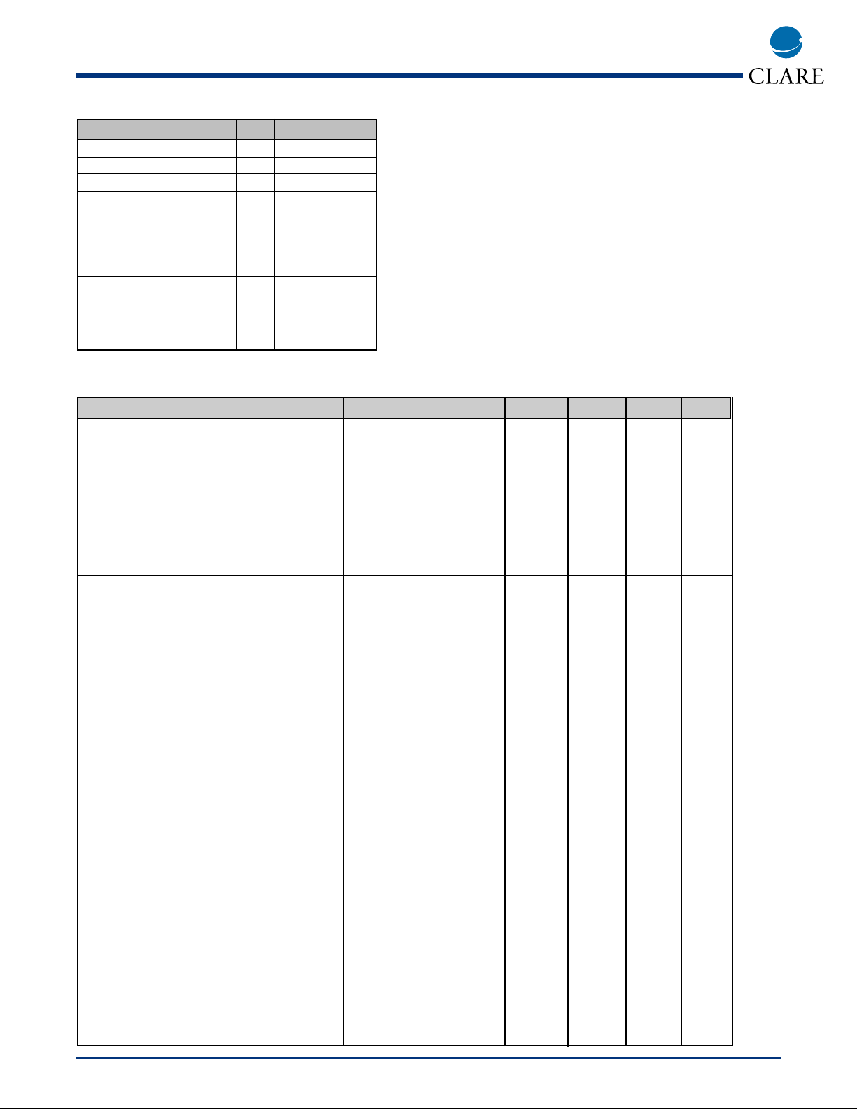
Electrical Characteristics
Absolute Maximum Ratings are stress ratings. Stresses
in excess of these ratings can cause permanent damage
to the device. Functional operation of the device at these
or any other conditions beyond those indicated in the
operational sections of this data sheet is not implied.
Exposure of the device to the absolute maximum ratings
for an extended period may degrade the device and effect
its reliability.
Absolute Maximum Ratings (@ 25˚ C)
2
Parameter Conditions Min Typ Max Unit
DC Electrical Characteristics
On-Hook Impedance @100VDC across pins 10 - - MΩ
10,11 (R,T), per FCC 68.312
Off-Hook Line Leakage Current @100VDC across pins - - 10 µA
10,11 (R,T), per FCC 68.312
Hookswitch Resistance - - - 15 Ω
Off-Hook Supply Current @+5V, V
CC
789mA
Hookswitch Power Source, Pin 8 - 4.75 5.0 20 V
DC Loop Current - 20 - 120 mA
AC Signal Path Electrical Characteristics
Return Loss 300-3500Hz 18 25 - dB
Insertion Loss
Transmit Test Circuit 1 - - 9 dB
Receive Test Circuit 2 - - 9 dB
Frequency Response 300-3500Hz -0.25 - +0.25 dB
Longitudinal Balance
On-Hook Per FCC 68.310 60 - - dB
Off-Hook Per FCC 68.310 40 - - dB
DC Loop Current - 20 - 120 mA
Total Harmonic Distortion + N @600Hz and -10dBm - -45 - dBm
Secondary Load Impedance Line 1 and Line 2 - 294 - Ω
Primary Source Impedance Tip and Ring - 600 - Ω
Ring Detection Circuit Characteristics
Ringing Voltage Detection Range - 20 - 150 V
RMS
Ringing Frequency Detection Range - 15 - 70 Hz
Ringer Equivalence Number - - 0.8B RING (Pin 9) Output Voltage (Pulsed) V
CC
@+5V
Logic ‘0’, Ring present - - 0.8 V
Logic ‘1’, Ring not present - - V
CC
V
Surge, Transient, and Isolation Characteristics
Surge Protection Voltage Tip and Ring
(Pins 11,10) - - - 300
Transient Voltage Protection on
Line 1 and Line 2 (Pins 1,2) - -5 - +5 V
Isolation Voltage
(Pins 1,2,7,8,9,17,18 to 10,11,13,14) Per FCC 68.302 - - 1000 V
RMS
Parameter Min Typ Max Units
Isolation Voltage - 1000 V
RMS
Operational Temperature 0 +70 °C
Storage Temperature 0 - +100 °C
Relative Humidity 10 - 85 %
(Non-Condensing)
Soldering Temperature - - +260 °C
Tip/Ring (5, 6) Load Current
(continuous) - - 120 mA
Hookswitch LED Drive Current - - 50 mA
Hookswitch LED Reverse Voltage - - 5 V
Ring Detect Phototransistor
Voltage V
CC
--20V
Page 3

CYG2911
www.clare.com
R1
3
Electrical Characteristics (Continued)
Parameter Conditions Min Typ Max Unit
911 Detection Characteristics (Pin 7)
Pulse Voltage
External phone off-hook - 2.4 - V
CC
V
External phone on-hook - - - 0.8 V
Pulse Width Telephone DCR 200Ω 20 40 60 mS
Internal pull-up resistor - - 200K - Ω
Top View
18
17
1
2
8
7
9
11
10
V
CC
GND
TIP
RING
14
13
CID1
CID2
LINE 1
LINE 2
911
OH
RING
CYG2911
1
2
13
14
VCC
µP Control
(Active Low)
CID1
CID2
CYG2911
Caller ID Connections
Pins 13 & 14 should be connected to a 1-Form-A
relay (Clare LCA110), as follows:
CYG2911 Pinouts & Definitions
PIN# I/O Name Function
1 I/O LINE1 Transformer isolated audio signal coupling path for the
telephone line.
2 I/O LINE2 Transformer isolated audio signal coupling path for the
telephone line.
7 O 911 Signals HIGH for 20-60ms when the CYG2911 is off-hook
and another phone goes off-hook. Glitches may appear on
this pin when the CYG2911 first goes off-hook, and should
be ignored for a minimum of 200ms.
8 I OH Driving this pin LOW asserts the off-hook condition. The
hookswitch LED is current limited by an internal 470Ω
resistor.
9 O RING Active LOW indicates an incoming ring signal. This is
pulsed LOW by the AC ring signal at the ring frequency
from 15-40Hz.
10 I/O RING Connection to telephone line Ring conductor.
11 I/O TIP Connection to telephone line Tip conductor.
13 O CID2 Caller ID connection. CID1/CID2 connect to an external 1-
Form-A solid state relay (Clare LCA110). When the SSR is
closed (connecting CID1 to CID2), Caller ID information is
presented to LINE1/LINE2 after the first telephone ring
burst.
14 O CID1 Caller ID connection. See CID2 above.
17 I GND Connected to host system ground.
18 I V
CC
Provides power to the hookswitch LED. Typically +5V for ≈
8mA LED current. LED is current limited by an internal
470Ω resistor. V
CC
should not exceed 20V.
Package Pinout
Page 4

CLARE LOCATIONS
Clare Headquarters
78 Cherry Hill Drive
Beverly, MA 01915
Tel: 1-978-524-6700
Fax: 1-978-524-4900
Toll Free: 1-800-27-CLARE
Clare Micronix Division
145 Columbia
Aliso Viejo, CA 92656-1490
Tel: 1-949-831-4622
Fax: 1-949-831-4628
SALES OFFICES
AMERICAS
Americas Headquarters
Clare
78 Cherry Hill Drive
Beverly, MA 01915
Tel: 1-978-524-6700
Fax: 1-978-524-4900
Toll Free: 1-800-27-CLARE
Eastern Region
Clare
P.O. Box 856
Mahwah, NJ 07430
Tel: 1-201-236-0101
Fax: 1-201-236-8685
Toll Free: 1-800-27-CLARE
Central Region
Clare Canada Ltd.
3425 Harvester Road, Suite 202
Burlington, Ontario L7N 3N1
Tel: 1-905-333-9066
Fax: 1-905-333-1824
Western Region
Clare
1852 West 11th Street, #348
Tracy, CA 95376
Tel: 1-209-832-4367
Fax: 1-209-832-4732
Toll Free: 1-800-27-CLARE
Canada
Clare Canada Ltd.
3425 Harvester Road, Suite 202
Burlington, Ontario L7N 3N1
Tel: 1-905-333-9066
Fax: 1-905-333-1824
EUROPE
European Headquarters
CP Clare nv
Bampslaan 17
B-3500 Hasselt (Belgium)
Tel: 32-11-300868
Fax: 32-11-300890
France
Clare France Sales
Lead Rep
99 route de Versailles
91160 Champlan
France
Tel: 33 1 69 79 93 50
Fax: 33 1 69 79 93 59
Germany
Clare Germany Sales
ActiveComp Electronic GmbH
Mitterstrasse 12
85077 Manching
Germany
Tel: 49 8459 3214 10
Fax: 49 8459 3214 29
Italy
C.L.A.R.E.s.a.s.
Via C. Colombo 10/A
I-20066 Melzo (Milano)
Tel: 39-02-95737160
Fax: 39-02-95738829
Sweden
Clare Sales
Comptronic AB
Box 167
S-16329 Spånga
Tel: 46-862-10370
Fax: 46-862-10371
United Kingdom
Clare UK Sales
Marco Polo House
Cook Way
Bindon Road
Taunton
UK-Somerset TA2 6BG
Tel: 44-1-823 352541
Fax: 44-1-823 352797
ASIA PACIFIC
Asian Headquarters
Clare
Room N1016, Chia-Hsin, Bldg II,
10F, No. 96, Sec. 2
Chung Shan North Road
Taipei, Taiwan R.O.C.
Tel: 886-2-2523-6368
Fax: 886-2-2523-6369
http://www.clare.com
Worldwide Sales Offices
Specification: DS-CYG2911-R1
©Copyright 2001, Clare, Inc.
All rights reserved. Printed in USA.
1/12/01
Clare cannot assume responsibility for use of any circuitry other
than circuitry entirely embodied in this Clare product. No circuit
patent licenses nor indemnity are expressed or implied. Clare
reserves the right to change the specification and circuitry, without notice at any time. The products described in this document
are not intended for use in medical implantation or other direct life
support applications where malfunction may result in direct physical harm, injury or death to a person.
 Loading...