

Page 1

Features
CY8CLED16
EZ-Color™ HB LED Controller
■ HB LED Controller
❐ Configurable Dimmers Support up to 16
Independent LED Channels
❐ 8-32 Bits of Resolution per Channel
❐ Dynamic Reconfiguration Enables LED
Controller plus other Features; Battery
Charging, Motor Control…
■ Visual Embedded Design, PSoC Express
❐ LED Based Express Drivers
• Binning Compensation
• Temperature Feedback
•DMX512
■ PrISM Modulation Technology
❐ Reduces Radiated EMI
❐ Reduces Low Frequency Blinking
■ Powerful Harvard Architecture Processor
❐ M8C Processor Speeds to 24 MHz
❐ 3.0 to 5.25V Operating Voltage
❐ Operating Voltages down to 1.0V using
On-Chip Switch Mode Pump (SMP)
❐ Industrial Temperature Range: -40°C to +85°C
■ Programmable Pin Configur ations
❐ 25 mA Sink on all GPIO
❐ Pull up, Pull down, High Z, Strong, or Open Drain Drive
Modes on all GPIO
❐ Up to eight Analog Inputs on GPIO
❐ Configurable Interrupt on all GPIO
■ Advanced Peripherals (PSoC Blocks)
❐ 16 Digital PSoC Blocks Provide:
• 8 to 32-Bit Timers, Counters, and PWMs
• Up to 2 Full-Duplex UART
• Multiple SPI™ Masters or Slaves
• Connectable to all GPIO Pins
❐ 12 Rail-to-Rail Analog PSoC Blocks Provide:
• Up to 14-Bit ADCs
• Up to 9-Bit DACs
• Programmable Gain Amplifiers
• Programmable Filters and Comparators
❐ Complex Peripherals by Combining Blocks
■ Flexible On-Chip Memory
❐ 32K Flash Program Storage 50,000 Erase/Write Cycles
❐ 2K SRAM Data Storage
❐ In-System Serial Programming (ISSP)
❐ Partial Flash Updates
❐ Flexible Protection Modes
❐ EEPROM Emulation in Flash
■ Complete Development Tools
❐ Free Development Software
• PSoC Designer™
• PSoC Express™
❐ Full-Featured, In-Circuit Emulator and
Programmer
❐ Full Speed Emulation
❐ Complex Breakpoint Structure
❐ 128 KBytes Trace Memory
EZ-Color HB LED Controller
Preliminary Data Sheet
Cypress Semiconductor Corporation •198 Champion Court•San Jose, CA 95134-1709•408-943-2600
Document Number: 001-13105 Rev. ** Revised June 12, 2007
Page 2
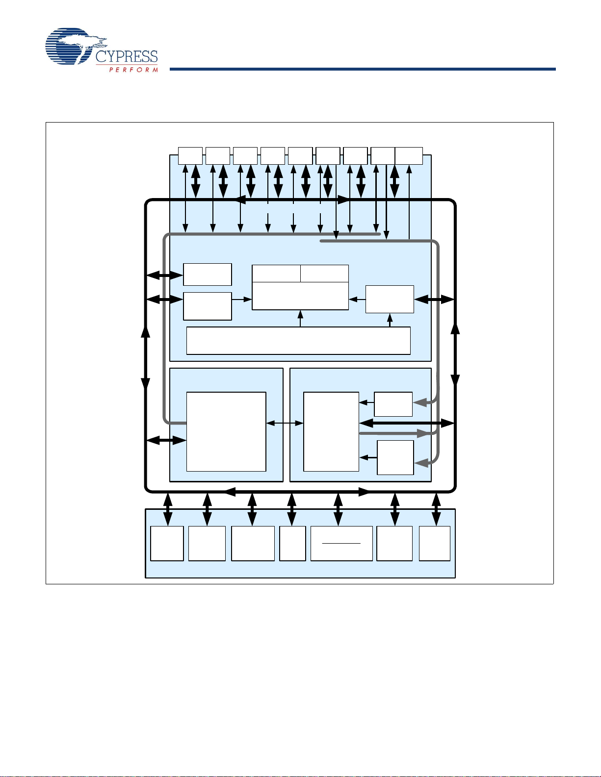
Overview
Block Diagram
Port 7 Port 6 Port 5 Port 4 Port 3 Port 2 Port 1 Port 0
SYSTEM BUS
CY8CLED16
Analog
Drivers
Global Digital Interconnect
SRAM
2K
Interrupt
Controller
SROM Flash 32K
CPU Core (M8C)
Multiple Clock Sources
(Includes IMO, ILO, PLL, and ECO)
DIGITAL SYSTEM
Digital
Block
Array
Global Analog Interconnect
PSoC CORE
Sleep and
Watchdog
ANALOG SYSTEM
Analog
Ref.
Analog
Block
Array
Analog
Input
Muxing
Digital
Clocks
Two
Multiply
Accums.
Decimator
2
I C
POR and LVD
System Resets
Internal
Voltage
Ref.
Switch
Mode
Pump
SYSTEM RESOURCES
Document Number: 001-13105 Rev. ** Page 2 of 39
Page 3

CY8CLED16
EZ-Color Functional Overview
Cypress' EZ-Color family of devices offers the ideal control
solution for High Brightness LED applications requiring intelligent dimming control. EZ-Color devices combine the power and
flexibility of PSoC (Programmable System-on-Chip™); with
Cypress' PrISM (precise illumination signal modulation)
modulation technology providing lighting designers a fully
customizable and integrated lighting solution platform.
The EZ-Color family supports up to 16 independent LED
channels with up to 32 bits of resolution per channel, enabling
lighting designers the flexibility to choose the LED array size and
color quality. PSoC Express software, with lighting specific
drivers, can significantly cut development time and simplify
implementation of fixed color points through temperature and
LED binning compensation. EZ-Color's virtually limitless analog
and digital customization allow for simple integration of features
in addition to intelligent lighting, such as Battery Charging, Image
Stabilization, and Motor Control during the development
process. These features, along with Cypress' best-in-class
quality and design support, make EZ-Color the ideal choice for
intelligent HB LED control applications.
Target Applications
■ LCD Backlight
■ Large Signs
■ General Lighting
■ Architectural Lighting
■ Camera/Cell Phone Flash
■ Flashlights
The PSoC Core
The PSoC Core is a powerful engine that supports a rich feature
set. The core includes a CPU, memory , clocks, and configurable
GPIO (General Purpose IO).
The M8C CPU core is a powerful processor with speeds up to 48
MHz, providing a four MIPS 8-bit Harvard architecture microprocessor. The CPU utilizes an interrupt controller with 25 vectors,
to simplify programming of real time embedded events. Program
execution is timed and protected using the included Sle ep and
Watch Dog Timers (WDT).
Memory encompasses 32 KB of Flash for program storage, 2 KB
of SRAM for data storage, and up to 2 KB of EEPROM emulated
using the Flash. Program Flash utilizes four protection levels on
blocks of 64 bytes, allowing customized software IP protection.
The EZ-Color family incorporates flexible internal clock generators, including a 24 MHz IMO (int ernal main oscill ator) accurate
to 2.5% over temperature and voltage. The 24 MHz IMO can also
be doubled to 48 MHz for use by the digital system. A low power
32 kHz ILO (internal low speed oscillator) is provided for the
Sleep timer and WDT. If crystal accuracy is desired, the ECO
(32.768 kHz external crystal oscillator) is available for use as a
Real Time Clock (RTC) and can optionally generate a
crystal-accurate 24 MHz system clock using a PLL. The clocks,
together with programmable clock dividers (as a System
Resource), provide the flexibility to integrate almost any timing
requirement into the EZ-Color device.
EZ-Color GPIOs provide connection to the CPU, digital and
analog resources of the device. Each pin’s drive mode may be
selected from eight options, allowing great flexibility in external
interfacing. Every pin also has the capability to generate a
system interrupt on high level, low level, and change from last
read.
The Digital System
The Digital System is composed of 16 digital PSoC blocks. Each
block is an 8-bit resource that can be used alone or combined
with other blocks to form 8, 16, 24, and 32-bit peripherals, which
are called user module references. Digital peripheral configurations include those listed below.
■ PrISM (8 to 32 bit)
■ PWMs (8 to 32 bit)
■ PWMs with Dead band (8 to 32 bit)
■ Counters (8 to 32 bit)
■ Timers (8 to 32 bit)
■ UART 8 bit with selectable parity (up to 4)
■ SPI master and slave (up to 4 each)
■ I2C slave and multi-master (1 available as a System Resource)
■ Cyclical Redundancy Checker/Generator (8 to 32 bit)
■ IrDA (up to 4)
■ Generators (8 to 32 bit)
The digital blocks can be connected to any GPIO through a
series of global buses that can route any signal to any pin. The
buses also allow for signal multiplexing and for performing logic
operations. This configurability frees your designs from the
constraints of a fixed peripheral controller.
Digital blocks are provided in rows of four, where the number of
blocks varies by EZ-Color device family. This allows you the
optimum choice of system resources for your application. Family
resources are shown in the table titled EZ-Color Device Characteristics on page 4.
Document Number: 001-13105 Rev. ** Page 3 of 39
Page 4
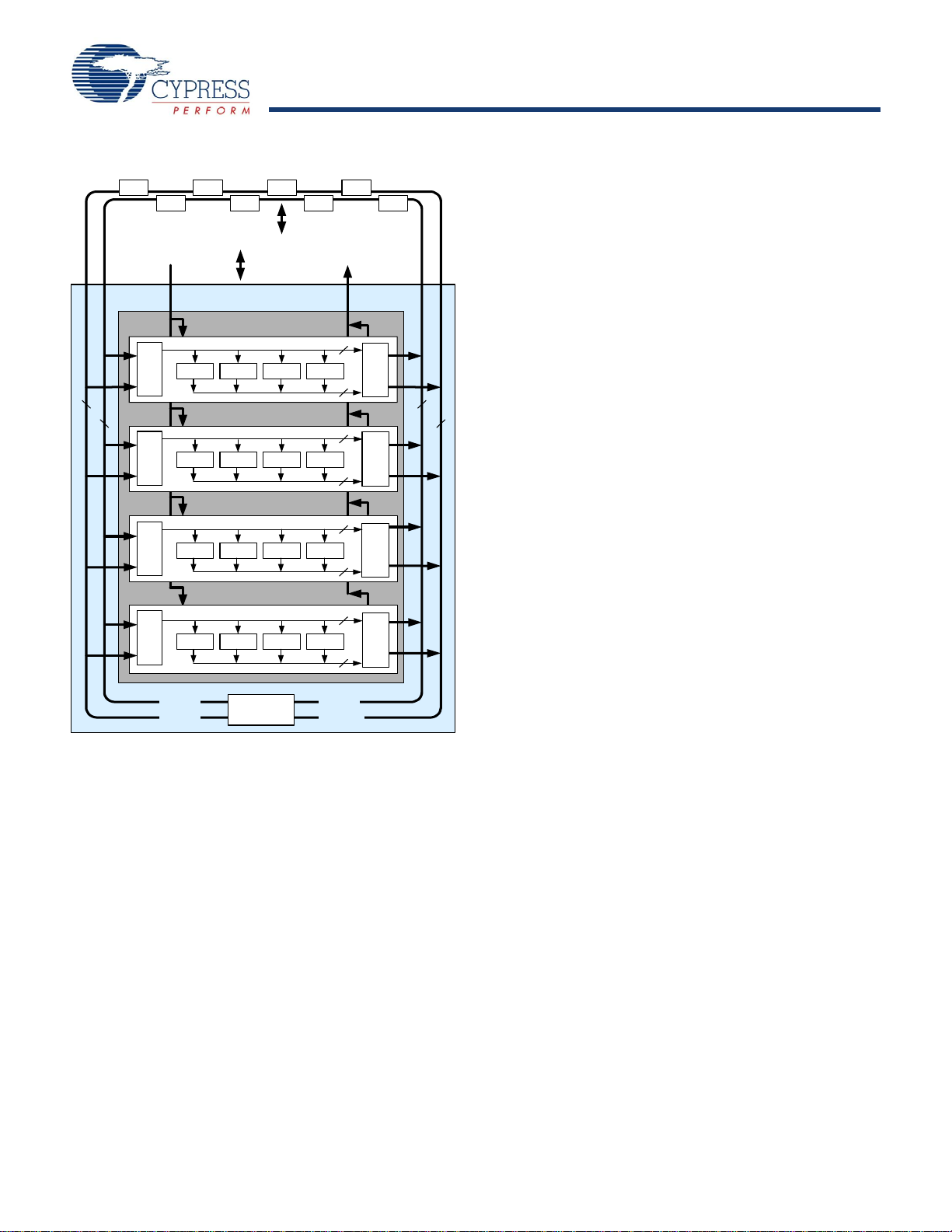
CY8CLED16
Figure 1. Digital System Block Diagram
Port 7
Port 6
Port 5
Port 4
Port 3
Port 2
Port 1
Port 0
The Analog System
The Analog System is composed of 12 configurable blocks, each
comprised of an opamp circuit allowing the creation of complex
analog signal flows. Analog peripherals are very flexible and can
l
o
c
k
o
r
e
To System Bus
s
To Analog
System
D
i
g
i
t
a
l
C
F
r
C
o
m
DIGITAL SYSTEM
Digital PSoC Block Array
Row 0
DBB00 DBB01 DCB02 DCB03
Row Input
8
Configuration
Row 1
DBB10 DBB11 DCB12 DCB13
Row Input
Configuration
Configuration
Row Output
4
4
8
Configuration
4
Row Output
4
be customized to support specific application requirements.
Some of the more common EZ-Color analog functions (most
available as user modules) are listed below.
■ Analog-to-digital converters (up to 4, with 6- to 14-bit resolution,
selectable as Incremental, Delta Sigma, and SAR)
■ Filters (2, 4, 6, or 8 pole band-pass, low-pass, and notch)
■ Amplifiers (up to 4, with selectable gain to 48x)
■ Instrumentation amplifiers (up to 2, with selectable gain to 93x)
■ Comparators (up to 4, with 16 selectable thresholds)
88
■ DACs (up to 4, with 6- to 9-bit resolution)
■ Multiplying DACs (up to 4, with 6- to 9-bit resolution)
■ High current output drivers (four with 40 mA drive as a Core
Resource)
Row 2
DBB20 DBB21 DCB22 DCB23
Row Input
Configuration
Row 3
DBB30 DBB31 DCB32 DCB33
Row Input
Configuration
Configuration
4
Row Output
4
Configuration
Row Output
4
4
■ 1.3V reference (as a System Resource)
■ DTMF Dialer
■ Modulators
■ Correlators
■ Peak Detectors
■ Many other topologies possible
Analog blocks are provided in columns of three, which includes
one CT (Continuous Time) and two SC (Switched Capacitor)
GIE[7:0]
GIO[7:0]
Global D ig ital
Interconnect
GOE[7:0]
GOO[7:0]
blocks, as shown in the figure below.
Document Number: 001-13105 Rev. ** Page 4 of 39
Page 5
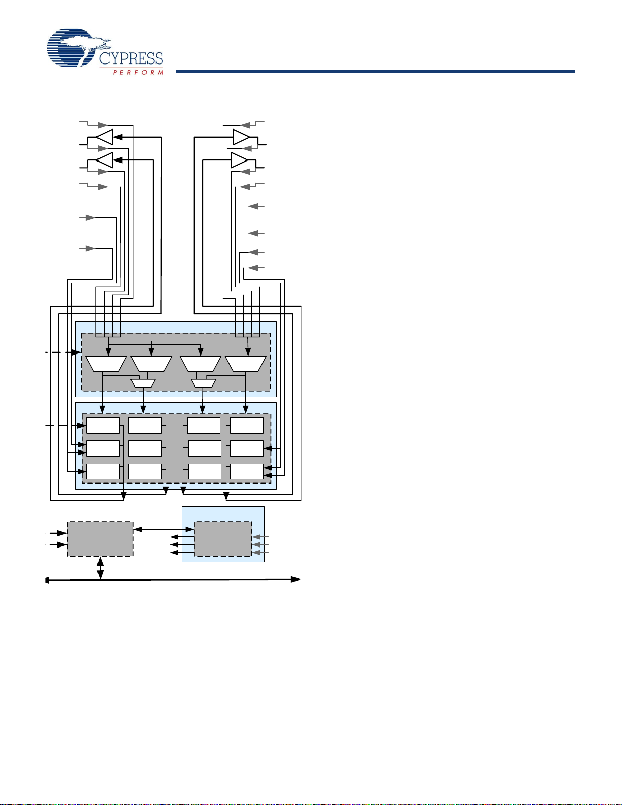
CY8CLED16
P0[7]
P0[5]
P0[3]
P0[1]
P2[3]
P2[1]
Figure 2. Analog System Block Diagram
RefIn
AGNDIn
Array Input Configuration
ACI0[1:0 ] ACI3[1:0 ]
ACB00 ACB01
ACI1[1:0] ACI2[1:0]
Block Array
ACB02 ACB03
P0[6]
P0[4]
P0[2]
P0[0]
P2[6]
P2[4]
P2[2]
P2[0]
Additional System Resources
System Resources, some of which have been previously listed,
provide additional capability useful to complete systems.
Resources include a multiplier, decimator, switch mode pump,
low voltage detection, and power on reset. Statements
describing the merits of each system resource are presented
below.
■ Digital clock dividers provide three customizable clock
frequencies for use in applications. The clocks can be routed
to both the digital and analog systems. Additional clocks can
be generated using digital PSoC blocks as clock dividers.
■ Multiply accumulate (MAC) provides fast 8-bit multiplier with
32-bit accumulate, to assist in general math and digital filters.
■ The decimator provides a custom hardware filter for digital
signal, processing applications including the creation of Delta
Sigma ADCs.
■ The I2C module provides 100 and 400 kHz communication over
two wires. Slave, master, and multi-master modes are all
supported.
■ Low Voltage Detection (LVD) interrupts can signal the appli-
cation of falling voltage levels, while the advanced POR (Power
On Reset) circuit eliminates the need for a system supervisor.
■ An internal 1.3 voltage reference provides an absolute
reference for the analog system, including ADCs and DACs.
■ An integrated switch mode pump (SMP) generates normal
operating voltages from a single 1.2V battery cell, providing a
low cost boost converter.
ASC10
Interface to
Digital System
M8C Interface (Address Bus, Data Bus, Etc.)
ASD11
ASC21
AGND
RefHi
RefLo
ASC12 ASD13
ASD22 ASC23ASD20
Analog Reference
Reference
Generators
AGNDIn
RefIn
Bandgap
Document Number: 001-13105 Rev. ** Page 5 of 39
Page 6
CY8CLED16
EZ-Color Device Characteristics
Depending on your EZ-Color device characteristics, the digital and analog systems can have 16, 8, or 4 digital blocks and 12, 6, or 4
analog blocks. The following table lists the resources available for specific EZ-Color device groups. The device covered by this data
sheet is shown in the highlighted row of the table.
Table 1. EZ-Color Device Characteristics
PSoC Part
Number
CY8CLED04 4 56 1 4 48 2 2 6 1K 16K Yes
CY8CLED08 8 44 2 8 12 4 4 12 256 Bytes 16K No
CY8CLED16 16 64 4 16 12 4 4 12 2K 32K No
LED
Channels
IO
Digital
Rows
Digital
Digital
Blocks
Analog
Inputs
Analog
Analog
Outputs
Columns
Analog
Blocks
Size
SRAM
Size
Flash
Getting Started
The quickest path to understanding the EZ-Color silicon is by
reading this data sheet and using PSoC Express to create HB
LED applications. This data sheet is an overview of the EZ-Color
integrated circuit and presents specific pin, register, and
electrical specifications.
For up-to-date Ordering, Packaging, and Electrical Specification
information, reference the latest device data sheets on the web
at http://www.cypress.com/ez-color.
Development Kits
Development Kits are available from the following distributors:
Digi-Key, A vnet, Arrow , and Future. The Cypress Online Store at
http://www.onfulfillment.com/cypressstore/ contains devel-
opment kits, C compilers, and all accessories for PSoC development. Click on EZ-Color to view a current list of available
items.
Technical Training Modules
Free PSoC technical training modules are available for users
new to PSoC. Training modules cover designing, debugging,
advanced analog, CapSense, and HB LED. Go to
http://www.cypress.com/techtrain.
Consultants
Certified PSoC Consultants offer everything from technical
assistance to completed PSoC designs. To contact or become a
PSoC Consultant, go to the following Cypress support web site:
http://www.cypress.com/support/cypros.cfm.
Technical Support
PSoC application engineers take pride in fast and accurate
response. They can be reached with a 4-hour guaranteed
response at http://www.cypress.com/support/login.cfm.
Application Notes
A long list of application notes will assist you i n every aspe ct of
your design effort. To view the PSoC application notes, go to the
http://www.cypress.com web site and select Application Notes
under the Design Resources list located in the center of the web
page. Application notes are listed by date by default.
CapSense
Document Number: 001-13105 Rev. ** Page 6 of 39
Page 7
CY8CLED16
Development Tools
PSoC Express is a high-level design tool for creating embedded
systems with devices using Cypress's PSoC Mixed-Signal
technology. With PSoC Express you create a complete
embedded solution including all necessary on-chip peripherals,
block configuration, interrupt handling and application software
without writing a single line of assembly or C code.
PSoC Express solves design problems the way you think about
the system:
■ Select input and output devices based upon system require-
ments.
■ Add a communications interface and define its interface to
system (using registers).
■ Define when and how an output device chang es state based
upon any and all other system devices.
■ Based upon the design, automatically select one or more PSoC
Mixed-Signal Controllers that match system requirements.
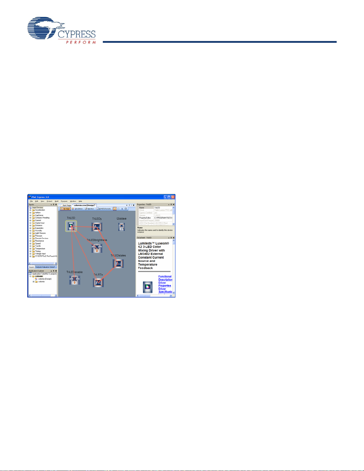
Figure 3. PSoC Express
Most of the files associated with a project are automatically
generated by PSoC Express during the build process, but you
can make changes directly to the custom.c and custom.h files
and also add your own custom code to the project in the Project
Manager.
Application Editor
The Application Editor allows you to edit custom.c and custom.h
as well as any C or assembly language source code that you add
to your project. With PSoC Express you can create application
software without writing a single line of assembly or C code, but
you have a full featured application editor at your finger tips if you
want it.
Build Manager
The Build Manager gives you the ability to build the application
software, assign pins, and generate the data sheet, schematic,
and BOM for your project.
Board Monitor
The Board Monitor is a debugging tool designed to be used
while attached to a prototype board through a communication
interface that allows you to monitor changes in the various
design elements in real time.
The default communication for the board monitor is I
2
the CY3240-I2USB I
C to USB Bridge Debugging/Communica-
tion Kit.
2
C. It uses
PSoC Express Subsystems
Express Editor
The Express Editor allows you to create designs visually by
dragging and dropping inputs, outputs, communication interfaces, and other design elements, and then describing the logic
that controls them.
Project Manager
The Project Manager allows you to work with your applications
and projects in PSoC Express. A PSoC Express application is a
top level container for projects and their associated files. Each
project contains a design that uses a single PSoC device. An
application can contain multiple projects so if you are creating an
application that uses multiple PSoC devices you can keep all of
the projects together in a single application.
Tuners
A Tuner is a visual interface for the Board Monitor that allows
you to view the performance of the HB LED drivers on your test
board while your program is running, and manually override values and see the results.
Hardware Tools
In-Circuit Emulator
A low cost, high functionality ICE (In-Circuit Emulator) is
available for development support. This hardware has the
capability to program single devices.
The emulator consists of a base unit that connects to the PC by
way of the USB port. The base unit is universal and will operate
with all PSoC devices. Emulation pods for each device family are
available separately. The emulation pod takes the place of the
PSoC device in the target board and performs full speed (24
MHz) operation.
2
I
C to USB Bridge
2
C to USB Bridge is a quick and easy link from any design
The I
or application’s I
debugging and communication.
2
C bus to a PC via USB for design testing,
Document Number: 001-13105 Rev. ** Page 7 of 39
Page 8
Document Conventions
CY8CLED16
Acronyms Used
The following table lists the acronyms that are used in this
document.
Acronym Description
AC alternating current
ADC analog-to-digital converter
API application programming interface
CPU central processing unit
CT continuous time
DAC digital-to-analog converter
DC direct current
ECO external crystal oscillator
EEPROM electrically erasable programmable read-only memory
FSR full scale range
GPIO general purpose IO
GUI graphical user interface
HBM human body model
ICE in-circuit emulator
ILO internal low speed oscillator
IMO internal main oscillator
IO input/output
IPOR imprecise power on reset
LSb least-significant bit
LVD low voltage detect
MSb most-significant bit
PC program counter
PLL phase-locked loop
POR power on reset
PPOR precision power on reset
PSoC™ Programmable System-on-Chip™
PWM pulse width modulator
SC switched capacitor
SLIMO slow IMO
SMP switch mode pump
SRAM static random access memory
Units of Measure
A units of measure table is located in the Electrical Specifications
section. Table 7 on page 15 lists all the abbreviations used to
measure the PSoC devices.
Numeric Naming
Hexidecimal numbers are represented with all letters in
uppercase with an appended lowercase ‘h’ (for example, ‘14h’ or
‘3Ah’). Hexidecimal numbers may also be represented by a ‘0x’
prefix, the C coding convention. Binary numbers have an
appended lowercase ‘b’ (e.g., 01010100b’ or ‘01000011b’).
Numbers not indicated by an ‘h’, ‘b’, or 0x are decimal.
Document Number: 001-13105 Rev. ** Page 8 of 39
Page 9
CY8CLED16
Pin Information
Pinouts
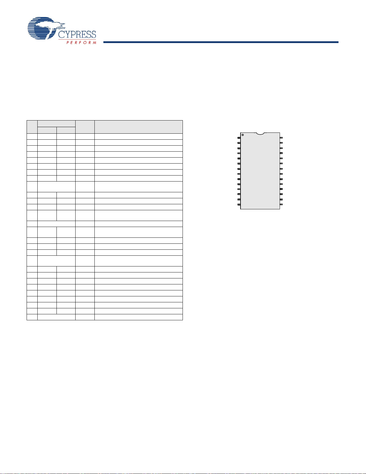
The CY8CLED16 device is available in three packages which are listed and illustrated in the following tables. Every port pin (labeled
with a “P”) is capable of Digital IO. However, Vss, Vdd, SMP, and XRES are not capable of Digital IO.
28-Pin Part Pinout
Table 2. 28-Pin Part Pinout (SSOP)
Pin
No.
1 IO I P0[7] Analog column mux input.
2 IO IO P0[5] Analog column mux input and column output.
3 IO IO P0[3] Analog column mux input and column output.
4 IO I P0[1] Analog column mux input.
5 IO P2[7]
6 IO P2[5]
7 IO I P2 [3 ] Direct switched capacitor block input.
8 IO I P2 [1 ] Direct switched capacitor block input.
9 Power SMP Switch Mode Pump (SMP) connection to
10 IO P1[7] I2C Serial Clock (SCL).
11 IO P1[5] I2C Serial Data (SDA).
12 IO P1[3]
13 IO P1[1] Crystal (XTALin), I2C Serial Clock (SCL),
14 Power Vss Ground connection.
15 IO P1[0] Crystal (XTALout), I2C Serial Data (SDA),
16 IO P1[2]
17 IO P1[4] Optional External Clock Input (EXTCLK).
18 IO P1[6]
19 Input XRES Active high external reset with internal pull
20 IO I P2[0] Direct switched capacitor block input.
21 IO I P2[2] Direct switched capacitor block input.
22 IO P2[4] External Analog Ground (AGND).
23 IO P2[6] External Voltage Reference (VREF).
24 IO I P0[0] Analog column mux input.
25 IO IO P0[2] Analog column mux input and column output.
26 IO IO P0[4] Analog column mux input and column output.
27 IO I P0[6] Analog column mux input.
28 Power Vdd Supply voltage.
Type
Digital Analog
Pin
Name
external components required.
ISSP-SCLK*.
ISSP-SDATA*.
down.
Description
A, I, P0[7]
A, IO, P0 [5 ]
A, IO, P0[3]
A, I, P0[1]
A, I, P2[1]
I2C SCL, P1[7]
I2C SDA, P1[5]
I2C SCL, XTALin, P1[1]
P2[7]
P2[5]
A, I,
P2[3]
SMP
P1[3]
Vss
10
11
12
13
14
28-Pin Device
1
2
3
4
5
6
7
8
9
SSOP
28
27
26
25
24
23
22
21
20
19
18
17
16
15
Vdd
P0[6], A, I
P0[4], A, IO
P0[2], A, IO
P0[0], A, I
P2[6], External VREF
P2[4], Extern a l AGND
P2[2], A, I
P2[0], A, I
XRES
P1[6]
P1[4], EXTCLK
P1[2]
P1[0], XTALout, I2C SDA
LEGEND: A = Analog, I = Input, and O = Output.
* These are the ISSP pins, which are not High Z at POR (Power On Reset).
Document Number: 001-13105 Rev. ** Page 9 of 39
Page 10
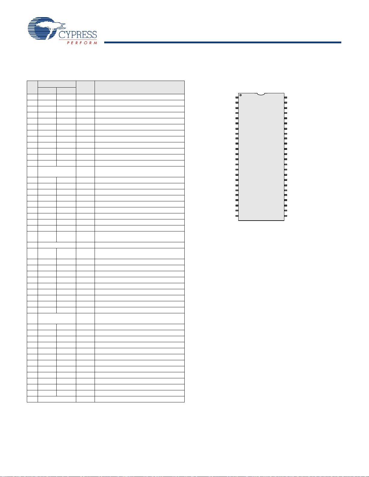
48-Pin Part Pinouts
Table 3. 48-Pin Part Pinout (SSOP)
Pin
No.
1 IO I P0[7] Analog column mux input.
2 IO IO P0[5] Analog column mux input and column output.
3 IO IO P0[3] Analog column mux input and column output.
4 IO I P0[1] Analog column mux input.
5 IO P2[7]
6 IO P2[5]
7 IO I P2[3] Direct switched capacitor block input.
8 IO I P2[1] Direct switched capacitor block input.
9 IO P4[7]
10 IO P4[5]
11 IO P4[3]
12 IO P4[1]
13 Power SMP Switch Mode Pump (SMP) connection to
14 IO P3[7]
15 IO P3[5]
16 IO P3[3]
17 IO P3[1]
18 IO P5[3]
19 IO P5[1]
20 IO P1[7] I2C Serial Clock (SCL).
21 IO P1[5] I2C Serial Data (SDA).
22 IO P1[3]
23 IO P1[1] Crystal (XTALin), I2C Serial Clock (SCL),
24 Power Vss Ground connecti on.
25 IO P1[0] Crystal (XTALout), I2C Serial Data (SDA),
26 IO P1[2]
27 IO P1[4] Optional External Clock Input (EXTCLK).
28 IO P1[6]
29 IO P5[0]
30 IO P5[2]
31 IO P3[0]
32 IO P3[2]
33 IO P3[4]
34 IO P3[6]
35 Input XRES Active high external reset with internal pull
36 IO P4[0]
37 IO P4[2]
38 IO P4[4]
39 IO P4[6]
40 IO I P2[0] Direct switched capacitor block input.
41 IO I P2[2] Direct switched capacitor block input.
42 IO P2[4] External Analog Ground (AGND).
43 IO P2[6] External Voltage Reference (VREF).
44 IO I P0[0] Analog column mux input.
45 IO IO P0[2] Analog column mux input and column output.
46 IO IO P0[4] Analog column mux input and column output.
47 IO I P0[6] Analog column mux input.
48 Power Vdd Supply voltage.
Type
Digital Analog
Pin
Name
external components required.
ISSP-SCLK*.
ISSP-SDATA*.
down.
Description
A, I, P0[7]
A, IO, P0[5]
A, IO, P0[3]
A, I, P0[1]
P2[7]
P2[5]
A, I, P2[3]
A, I, P2 [1 ]
P4[7]
P4[5]
P4[3]
P4[1]
SMP
P3[7]
P3[5]
P3[3]
P3[1]
P5[3]
P5[1]
I2C SCL , P1[7]
I2C SDA, P1[5]
I2C SCL, X TALin, P1 [1 ]
P1[3]
Vss
48-Pin Device
1
2
3
4
5
6
7
8
9
10
11
12
SSOP
13
14
15
16
17
18
19
20
21
22
23
24
CY8CLED16
Vdd
48
P0[6], A, I
47
P0[4], A, IO
46
P0[2], A, IO
45
P0[0], A, I
44
P2[6], External VREF
43
P2[4], E x te r n a l A GND
42
P2[2], A, I
41
P2[0], A, I
40
P4[6]
39
P4[4]
38
P4[2]
37
P4[0]
36
XRES
35
P3[6]
34
P3[4]
33
P3[2]
32
P3[0]
31
P5[2]
30
P5[0]
29
P1[6]
28
P1[4], EXTCLK
27
P1[2]
26
P1[0], X T A Lout, I2 C SDA
25
LEGEND: A = Analog, I = Input, and O = Output.
* These are the ISSP pins, which are not High Z at POR (Power On Reset).
Document Number: 001-13105 Rev. ** Page 10 of 39
Page 11
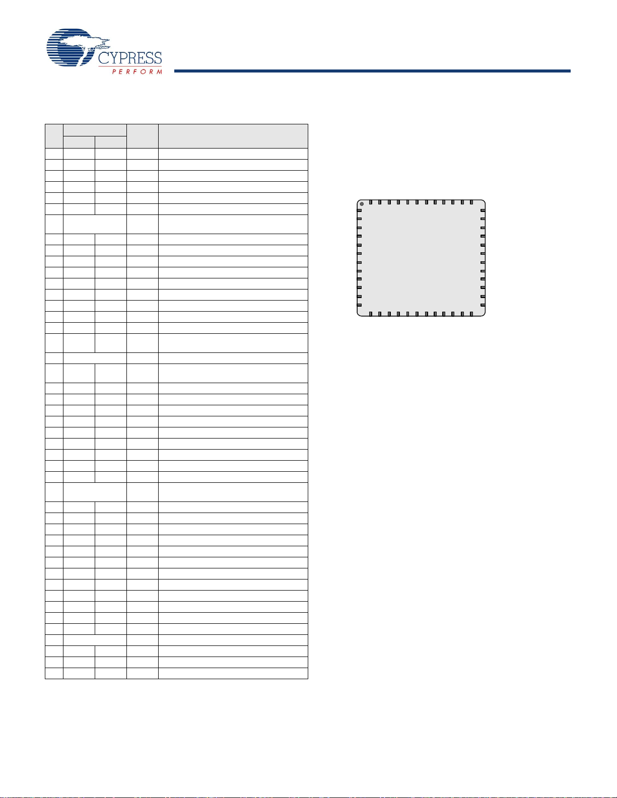
Table 4. 48-Pin Part Pinout (QFN**)
Pin
No.
1 IO I P2[3] Direct switched capacitor block input.
2 IO I P2[1] Direct switched capacitor block input.
3 IO P4[7]
4 IO P4[5]
5 IO P4[3]
6 IO P4[1]
7 Power SMP Switch Mode Pump (SMP) connection to
8 IO P3[7]
9 IO P3[5]
10 IO P3[3]
11 IO P3[1]
12 IO P5[3]
13 IO P5[1]
14 IO P1[7] I2C Serial Clock (SCL).
15 IO P1[5] I2C Serial Data (SDA).
16 IO P1[3]
17 IO P1[1] Crystal (XTALin), I2C Serial Clock (SCL),
18 Power Vss Ground connection.
19 IO P1[0] Crystal (XTALout), I2C Serial Data (SDA),
20 IO P1[2]
21 IO P1[4] Optional External Clock Input (EXTCLK).
22 IO P1[6]
23 IO P5[0]
24 IO P5[2]
25 IO P3[0]
26 IO P3[2]
27 IO P3[4]
28 IO P3[6]
29 Input XRES Active high external reset with internal pull
30 IO P4[0]
31 IO P4[2]
32 IO P4[4]
33 IO P4[6]
34 IO I P2[0] Direct switched capacitor block input.
35 IO I P2[2] Direct switched capacitor block input.
36 IO P2[4] External Analog Ground (AGND).
37 IO P2[6] External Voltage Reference (VREF).
38 IO I P0[0] Analog column mux input.
39 IO IO P0[2] Analog column mux input and column output.
40 IO IO P0[4] Analog column mux input and column output.
41 IO I P0[6] Analog column mux input.
42 Power Vdd Supply voltage.
43 IO I P0[7] Analog column mux input.
44 IO IO P0[5] Analog column mux input and column output.
45 IO IO P0[3] Analog column mux input and column output.
Type
Digital Analog
Pin
Name
external components required.
ISSP-SCLK*.
ISSP-SDATA*.
down.
Description
A, I, P2[3]
A, I, P2[1]
P4[7]
P4[5]
P4[3]
P4[1]
SMP
P3[7]
P3[5]
P3[3]
P3[1]
P5[3]
48-Pin PSoC Device
P2[5]
P2[7]
P0[1], A, I
P0[3], A, IO
P0[5], A, IO
P0[7], A, I
4847464544
1
2
3
4
5
6
7
8
9
10
11
12
131415161718192021
P5[1]
I2C SCL, P1[7]
43424140393837
MLF
(Top View)
Vss
P1[3]
I2C SDA, P1[5]
I2C SCL, XTALin, P1[1]
CY8CLED16
Vdd
P0[6], A, I
P0[4], A, IO
P0[2], A, IO
P0[0], A, I
P2[6], External VREF
P2[4], Extern a l A GND
36
35
P2[2], A, I
34
P2[0], A, I
33
P4[6]
32
P4[4]
31
P4[2]
30
P4[0]
29
XRES
28
P3[6]
P3[4]
27
26
P3[2]
25
22
P1[2]
P1[6]
EXTCLK, P1[4]
I2C SDA, XTALout, P1[0]
P3[0]
23
24
P5[0]
P5[2]
Document Number: 001-13105 Rev. ** Page 11 of 39
Page 12
Table 4. 48-Pin Part Pinout (QFN**)
46 IO I P0[1] Analog column mux input.
47 IO P2[7]
48 IO P2[5]
LEGEND: A = Analog, I = Input, and O = Output.
* These are the ISSP pins, which are not High Z at POR (Power On Reset).
** The QFN package has a center pad that must be connected to ground (Vss).
Register Reference
CY8CLED16
Register Conventions
Abbreviations Used
The register conventions specific to this section are listed in the
following table.
Register Mapping Tables
This chapter lists the registers of the CY8CLED16 EZ-Color
device.
The device has a total register address space of 512 bytes. The
register space is referred to as IO space and is divided into two
banks. The XOI bit in the Flag register (CPU_F) determines
Convention Description
R Read register or bit(s)
W Write register or bit(s)
L Logical register or bit(s)
C Clearable register or bit(s)
# Access is bit specific
which bank the user is currently in. When the XOI bit is set the
user is in Bank 1.
Note In the following register mapping tables, blank fields are
reserved and should not be accessed.
Table 5. Register Map Bank 0 Table: User Space
Name Addr (0,Hex) Access Name Addr (0,Hex) Access Name Addr (0,Hex)
PRT0DR 00 RW DBB20DR0 40 # ASC10CR0 80 RW RDI2RI C0 RW
PRT0IE 01 RW DBB20DR1 41 W ASC10CR1 81 RW RDI2SYN C1 RW
PRT0GS 02 RW DBB20DR2 42 RW ASC10CR2 82 RW RDI2IS C2 RW
PRT0DM2 03 RW DBB20CR0 43 # ASC10CR3 83 RW RDI2LT0 C3 RW
PRT1DR 04 RW DBB21DR0 44 # ASD11CR0 84 RW RDI2LT1 C4 RW
PRT1IE 05 RW DBB21DR1 45 W ASD11CR1 85 RW RDI2RO0 C5 RW
PRT1GS 06 RW DBB21DR2 46 RW ASD11CR2 86 RW RDI2RO1 C6 RW
PRT1DM2 07 RW DBB21CR0 47 # ASD11CR3 87 RW C7
PRT2DR 08 RW DCB22DR0 48 # ASC12CR0 88 RW RDI3RI C8 RW
PRT2IE 09 RW DCB22DR1 49 W ASC12CR1 89 RW RDI3SYN C9 RW
PRT2GS 0A RW DCB22DR2 4A RW ASC12CR2 8A RW RDI3IS CA RW
PRT2DM2 0B RW DCB22CR0 4B # ASC12CR3 8B RW RDI3LT0 CB RW
PRT3DR 0C RW DCB23DR0 4C # ASD13CR0 8C RW RDI3LT1 CC RW
PRT3IE 0D RW DCB23DR1 4D W ASD13CR1 8D RW RDI3RO0 CD RW
PRT3GS 0E RW DCB23DR2 4E RW ASD13CR2 8E RW RDI3RO1 CE RW
PRT3DM2 0F RW DCB23CR0 4F # ASD13CR3 8F RW CF
PRT4DR 10 RW DBB30DR0 50 # ASD20CR0 90 RW CUR_PP D0 RW
PRT4IE 11 RW DBB30DR1 51 W ASD20CR1 91 RW STK_PP D1 RW
PRT4GS 12 RW DBB30DR2 52 RW ASD20CR2 92 RW D2
PRT4DM2 13 RW DBB30CR0 53 # ASD20CR3 93 RW IDX_PP D3 RW
PRT5DR 14 RW DBB31DR0 54 # ASC21CR0 94 RW MVR_PP D4 RW
PRT5IE 15 RW DBB31DR1 55 W ASC21CR1 95 RW MVW_PP D5 RW
PRT5GS 16 RW DBB31DR2 56 RW ASC21CR2 96 RW I2C_CFG D6 RW
PRT5DM2 17 RW DBB31CR0 57 # ASC21CR3 97 RW I2C_SCR D7 #
PRT6DR 18 RW DCB32DR0 58 # ASD22CR0 98 RW I2C_DR D8 RW
PRT6IE 19 RW DCB32DR1 59 W ASD22CR1 99 RW I2C_MSCR D9 #
PRT6GS 1A RW DCB32DR2 5A RW ASD22CR2 9A RW INT_CLR0 DA RW
PRT6DM2 1B RW DCB32CR0 5B # ASD22CR3 9B RW INT_CLR1 DB RW
PRT7DR 1C RW DCB33DR0 5C # ASC23CR0 9C RW INT_CLR2 DC RW
PRT7IE 1D RW DCB33DR1 5D W ASC23CR1 9D RW INT_CLR3 DD RW
Blank fields are Reserved and should not be accessed. # Access is bit specific.
Acces
Name Addr (0,Hex)
Acces
Document Number: 001-13105 Rev. ** Page 12 of 39
Page 13

CY8CLED16
Table 5. Register Map Bank 0 Table: User Space (continued)
Name Addr (0,Hex) Access Name Addr (0,Hex) Access Name Addr (0,Hex)
PRT7GS 1E RW DCB33DR2 5E RW ASC23CR2 9E RW INT_MSK3 DE RW
PRT7DM2 1F RW DCB33CR0 5F # ASC23CR3 9F RW INT_MSK2 DF RW
DBB00DR0 20 # AMX_IN 60 RW A0 INT_MSK0 E0 RW
DBB00DR1 21 W 61 A1 INT_MSK1 E1 RW
DBB00DR2 22 RW 62 A2 INT_VC E2 RC
DBB00CR0 23 # ARF_CR 63 RW A3 RES_WDT E3 W
DBB01DR0 24 # CMP_CR0 64 # A4 DEC_DH E4 RC
DBB01DR1 25 W ASY_CR 65 # A5 DEC_DL E5 RC
DBB01DR2 26 RW CMP_CR1 66 RW A6 DEC_CR0 E6 RW
DBB01CR0 27 # 67 A7 DEC_CR1 E7 RW
DCB02DR0 28 # 68 MUL1_X A8 W MUL0_X E8 W
DCB02DR1 29 W 69 MUL1_Y A9 W MUL0_Y E9 W
DCB02DR2 2A RW 6A MUL1_DH AA R MUL0_DH EA R
DCB02CR0 2B # 6B MUL1_DL AB R MUL0_DL EB R
DCB03DR0 2C # TMP_DR0 6C RW ACC1_DR1 AC RW ACC0_DR1 EC RW
DCB03DR1 2D W TMP_DR1 6D RW ACC1_DR0 AD RW ACC0_DR0 ED RW
DCB03DR2 2E RW TMP_DR2 6E RW ACC1_DR3 AE RW ACC0_DR3 EE RW
DCB03CR0 2F # TMP_DR3 6F RW ACC1_DR2 AF RW ACC0_DR2 EF RW
DBB10DR0 30 # ACB00CR3 70 RW RDI0RI B0 RW F0
DBB10DR1 31 W ACB00CR0 71 RW RDI0SYN B1 RW F1
DBB10DR2 32 RW ACB00CR1 72 RW RDI0IS B2 RW F2
DBB10CR0 33 # ACB00CR2 73 RW RDI0LT0 B3 RW F3
DBB11DR0 34 # ACB01CR3 74 RW RDI0LT1 B4 RW F4
DBB11DR1 35 W ACB01CR0 75 RW RDI0RO0 B5 RW F5
DBB11DR2 36 RW ACB01CR1 76 RW RDI0RO1 B6 RW F6
DBB11CR0 37 # ACB01CR2 77 RW B7 CPU_F F7 RL
DCB12DR0 38 # ACB02CR3 78 RW RDI1RI B8 RW F8
DCB12DR1 39 W ACB02CR0 79 RW RDI1SYN B9 RW F9
DCB12DR2 3A RW ACB02CR1 7A RW RDI1IS BA RW FA
DCB12CR0 3B # ACB02CR2 7B RW RDI1LT0 BB RW FB
DCB13DR0 3C # ACB03CR3 7C RW RDI1LT1 BC RW FC
DCB13DR1 3D W ACB03CR0 7D RW RDI1RO0 BD RW FD
DCB13DR2 3E RW ACB03CR1 7E RW RDI1RO1 BE RW CPU_SCR1 FE #
DCB13CR0 3F # ACB03CR2 7F RW BF CPU_SCR0 FF #
Blank fields are Reserved and should not be accessed. # Access is bit specific.
Acces
Name Addr (0,Hex)
Acces
Table 6. Register Map Bank 1 Table: Configuration Space
Name Addr(1,Hex) Access Name Addr(1,Hex) Access Name Addr(1,Hex)
PRT0DM0 00 RW DBB20FN 40 RW ASC10CR0 80 RW RDI2RI C0 RW
PRT0DM1 01 RW DBB20IN 41 RW ASC10CR1 81 RW RDI2SYN C1 RW
PRT0IC0 02 RW DBB20OU 42 RW ASC10CR2 82 RW RDI2IS C2 RW
PRT0IC1 03 RW 43 ASC10CR3 83 RW RDI2LT0 C3 RW
PRT1DM0 04 RW DBB21FN 44 RW ASD11CR0 84 RW RDI2LT1 C4 RW
PRT1DM1 05 RW DBB21IN 45 RW ASD11CR1 85 RW RDI2RO0 C5 RW
PRT1IC0 06 RW DBB21OU 46 RW ASD11CR2 86 RW RDI2RO1 C6 RW
PRT1IC1 07 RW 47 ASD11CR3 87 RW C7
PRT2DM0 08 RW DCB22FN 48 RW ASC12CR0 88 RW RDI3RI C8 RW
PRT2DM1 09 RW DCB22IN 49 RW ASC12CR1 89 RW RDI3SYN C9 RW
PRT2IC0 0A RW DCB22OU 4A RW ASC12CR2 8A RW RDI3IS CA RW
PRT2IC1 0B RW 4B ASC12CR3 8B RW RDI3LT0 CB RW
PRT3DM0 0C RW DCB23FN 4C RW ASD13CR0 8C RW RDI3LT1 CC RW
PRT3DM1 0D RW DCB23IN 4D RW ASD13CR1 8D RW RDI3RO0 CD RW
PRT3IC0 0E RW DCB23OU 4E RW ASD13CR2 8E RW RDI3RO1 CE RW
PRT3IC1 0F RW 4F ASD13CR3 8F RW CF
PRT4DM0 10 RW DBB30FN 50 RW ASD20CR0 90 RW GDI_O_IN D0 RW
PRT4DM1 11 RW DBB30IN 51 RW ASD20CR1 91 RW GDI_E_IN D1 RW
PRT4IC0 12 RW DBB30OU 52 RW ASD20CR2 92 RW GDI_O_OU D2 RW
PRT4IC1 13 RW 53 ASD20CR3 93 RW GDI_E_OU D3 RW
PRT5DM0 14 RW DBB31FN 54 RW ASC21CR0 94 RW D4
PRT5DM1 15 RW DBB31IN 55 RW ASC21CR1 95 RW D5
PRT5IC0 16 RW DBB31OU 56 RW ASC21CR2 96 RW D6
PRT5IC1 17 RW 57 ASC21CR3 97 RW D7
Blank fields are Reserved and should not be accessed. # Access is bit specific.
Acces
s
Name Addr(1,Hex)
Acces
Document Number: 001-13105 Rev. ** Page 13 of 39
s
Page 14

CY8CLED16
Table 6. Register Map Bank 1 Table: Configuration Space (continued)
Name Addr(1,Hex) Access Name Addr(1,Hex) Access Name Addr(1,Hex)
PRT6DM0 18 RW DCB32FN 58 RW ASD22CR0 98 RW D8
PRT6DM1 19 RW DCB32IN 59 RW ASD22CR1 99 RW D9
PRT6IC0 1A RW DCB32OU 5A RW ASD22CR2 9A RW DA
PRT6IC1 1B RW 5B ASD22CR3 9B RW DB
PRT7DM0 1C RW DCB33FN 5C RW ASC23CR0 9C RW DC
PRT7DM1 1D RW DCB33IN 5D RW ASC23CR1 9D RW OSC_GO_EN DD RW
PRT7IC0 1E RW DCB33OU 5E RW ASC23CR2 9E RW OSC_CR4 DE RW
PRT7IC1 1F RW 5F ASC23CR3 9F RW OSC_CR3 DF RW
DBB00FN 20 RW CLK_CR0 60 RW A0 OSC_CR0 E0 RW
DBB00IN 21 RW CLK_CR1 61 RW A1 OSC_CR1 E1 RW
DBB00OU 22 RW ABF_CR0 62 RW A2 OSC_CR2 E2 RW
23 AMD_CR0 63 RW A3 VLT_CR E3 RW
DBB01FN 24 RW 64 A4 VLT_CMP E4 R
DBB01IN 25 RW 65 A5 E5
DBB01OU 26 RW AMD_CR1 66 RW A6 E6
27 ALT_CR0 67 RW A7 DEC_CR2 E7 RW
DCB02FN 28 RW ALT_CR1 68 RW A8 IMO_TR E8 W
DCB02IN 29 RW CLK_CR2 69 RW A9 ILO_TR E9 W
DCB02OU 2A RW 6A AA BDG_TR EA RW
2B 6B AB ECO_TR EB W
DCB03FN 2C RW TMP_DR0 6C RW AC EC
DCB03IN 2D RW TMP_DR1 6D RW AD ED
DCB03OU 2E RW TMP_DR2 6E RW AE EE
2F TMP_DR3 6F RW AF EF
DBB10FN 30 RW ACB00CR3 70 RW RDI0RI B0 RW F0
DBB10IN 31 RW ACB00CR0 71 RW RDI0SYN B1 RW F1
DBB10OU 32 RW ACB00CR1 72 RW RDI0IS B2 RW F2
33 ACB00CR2 73 RW RDI0LT0 B3 RW F3
DBB11FN 34 RW ACB01CR3 74 RW RDI0LT1 B4 RW F4
DBB11IN 35 RW ACB01CR0 75 RW RDI0RO0 B5 RW F5
DBB11OU 36 RW ACB01CR1 76 RW RDI0RO1 B6 RW F6
37 ACB01CR2 77 RW B7 CPU_F F7 RL
DCB12FN 38 RW ACB02CR3 78 RW RDI1RI B8 RW F8
DCB12IN 39 RW ACB02CR0 79 RW RDI1SYN B9 RW F9
DCB12OU 3A RW ACB02CR1 7A RW RDI1IS BA RW FLS_PR1 FA RW
3B ACB02CR2 7B RW RDI1LT0 BB RW FB
DCB13FN 3C RW ACB03CR3 7C RW RDI1LT1 BC RW FC
DCB13IN 3D RW ACB03CR0 7D RW RDI1RO0 BD RW FD
DCB13OU 3E RW ACB03CR1 7E RW RDI1RO1 BE RW CPU_SCR1 FE #
3F ACB03CR2 7F RW BF CPU_SCR0 FF #
Blank fields are Reserved and should not be accessed. # Access is bit specific.
Acces
s
Name Addr(1,Hex)
Acces
s
Document Number: 001-13105 Rev. ** Page 14 of 39
Page 15

CY8CLED16
Electrical Specifications
This chapter presents the DC and AC electrical specifications of the CY8CLED16 EZ-Color device. For the most up to date electrical
specifications, confirm that you have the most recent data sheet by going to the web at
http://www.cypress.com/ez-color.
Specifications are valid for -40oC ≤ TA ≤ 85oC and TJ ≤ 100oC, except where noted. Refer to T able 23 for the electrical specifications
on the internal main oscillator (IMO) using SLIMO mode.
Figure 4. Voltage versus CPU Frequency, and IMO Frequency Trim Options
5.25
4.75
Vdd Voltage
3.00
O
V
p
a
l
e
Re
i
d
r
a
t
g
i
n
i
o
g
n
93 kHz 12 MHz 24 MHz
CPU Frequency
5.25
4.75
Vdd Voltage
3.60
3.00
The following table lists the units of measure that are used in this chapter.
Table 7. Units of Measure
Symbol Unit of Measure Symbol Unit of Measure
o
degree Celsius μW microwatts
C
dB decibels mA milli-ampere
fF femto farad ms milli-second
Hz hertz mV milli-volts
KB 1024 bytes nA nanoampere
Kbit 1024 bits ns nanosecond
kHz kilohertz nV nanovolts
kΩ kilohm Ω ohm
MHz megahertz pA picoampere
MΩ megaohm pF picofarad
μA microampere pp peak-to-peak
μF microfarad ppm parts per million
μH microhenry ps picosecond
μs microsecond sps samples per second
μV microvolts σ sigma: one standard deviation
μVrms microvolts root-mean-square V volts
93 kHz
SLIMO
Mode=1
SLIMO Mode = 0
SLIMO
Mode=1
6 MHz
IMO Frequency
SLIMO
Mode=0
SLIMO
Mode=0
12 MHz 24 MHz
Document Number: 001-13105 Rev. ** Page 15 of 39
Page 16

Absolute Maximum Ratings
Table 8. Absolute Maximum Ratings
Symbol Description Min Typ Max Units Notes
T
STG
T
A
Storage Temperature -55 25 +100
Ambient Temperature with Power Applied -40 – +85
Vdd Supply Voltage on Vdd Relative to Vss -0.5 – +6.0 V
V
IO
V
IOZ
I
MIO
I
MAIO
DC Input Voltage Vss - 0.5 – Vdd + 0.5 V
DC Voltage Applied to Tri-state Vss - 0.5 – Vdd + 0.5 V
Maximum Current into any Port Pin -25 – +50 mA
Maximum Current into any Port Pin Configured as Analog
Driver
-50 – +50 mA
ESD Electro Static Discharge Voltage 2000 – – V Human Body Model ESD.
LU Latch-up Current – – 200 mA
o
C
o
C
Higher storage temperatures will reduce data
retention time. Recommended storage temper-
ature is +25
age temperatures above 65
reliability.
o
C ± 25oC. Extended duration stor-
CY8CLED16
o
C will degrade
Operating Temperature
Table 9. Operating Temperature
Symbol Description Min Typ Max Units Notes
T
A
T
J
Ambient Temperature -40 – +85
Junction Temperature -40 – +100
o
C
o
C
The temperature rise from ambient to junction
is package specific. See “Thermal Impedances
per Package” on page 36. The user must limit
the power consumption to comply with this
requirement.
Document Number: 001-13105 Rev. ** Page 16 of 39
Page 17

CY8CLED16
DC Electrical Characteristics
DC Chip-Level Specifications
The following table lists guaranteed maximum and min imum specificat ions for the voltage and tempera ture ranges: 4.75V to 5.25V
and -40°C ≤ T
are for design guidance only.
Table 10. DC Chip-Level Specifications
Symbol Description Min Typ Max Units Notes
Vdd Supply Voltage 3.00 – 5.25 V See DC POR and LVD specifications,
I
DD
I
DD3
I
DDP
I
SB
I
SBH
I
SBXTL
I
SBXTLH
V
REF
≤ 85°C, or 3.0V to 3.6V and -40°C ≤ TA ≤ 85°C, respectively. Typical parameters apply to 5V and 3.3V at 25°C and
A
Table 3-15 on page 27.
Supply Current – 8 14 mA
Supply Current – 5 9 mA
Supply current when IMO = 6 MHz using SLIMO mode. – 2 3 mA
Sleep (Mode) Current with POR, L VD, Sleep Timer, WDT,
and internal slow oscillator active.
Sleep (Mode) Current with POR, L VD, Sleep Timer, WDT,
and internal slow oscillator active.
Sleep (Mode) Current with POR, L VD, Sleep Timer, WDT,
internal slow oscillator, and 32 kHz crystal oscillator active.
Sleep (Mode) Current with POR, L VD, Sleep Timer, WDT,
and 32 kHz crystal oscillator active.
Reference Voltage (Bandgap) 1.28 1.3 1.32 V Trimmed for appropriate Vdd.
– 3 10 μA Conditions are with internal slow speed oscilla-
– 4 25 μA Conditions are with internal slow speed oscilla-
– 4 12 μA Conditions are with properly loaded, 1 μW max,
– 5 27 μA Conditions are with properly loaded, 1 μW max,
Conditions are 5.0V, TA = 25 oC, CPU = 3 MHz,
SYSCLK doubler disabled, VC1 = 1.5 MHz,
VC2 = 93.75 kHz, VC3 = 0.366 kHz.
Conditions are Vdd = 3.3V, TA = 25 oC, CPU = 3
MHz, SYSCLK doubler disabled, VC1 = 1.5
MHz, VC2 = 93.75 kHz, VC3 = 0.366 kHz.
Conditions are Vdd = 3.3V, TA = 25 oC, CPU =
0.75 MHz, SYSCLK doubler disabled, VC1 =
0.375 MHz, VC2 = 23.44 kHz, VC3 = 0.09 kHz.
o
tor, Vdd = 3.3V, -40
tor, Vdd = 3.3V, 55
32.768 kHz crystal. Vdd = 3.3V, -40
o
C.
55
32.768 kHz crystal. Vdd = 3.3V, 55
o
C.
C ≤ TA ≤ 55 oC.
o
C < TA ≤ 85 oC.
o
C ≤ TA ≤
o
C < TA ≤ 85
DC General Purpose IO Specifications
The following table lists guaranteed maximum and min imum specificat ions for the voltage and tempera ture ranges: 4.75V to 5.25V
and -40°C ≤ T
are for design guidance only.
≤ 85°C, or 3.0V to 3.6V and -40°C ≤ TA ≤ 85°C, respectively. Typical parameters apply to 5V and 3.3V at 25°C and
A
Table 11. DC GPIO Specifications
Symbol Description Min Typ Max Units Notes
R
PU
R
PD
V
OH
V
OL
V
IL
V
IH
V
H
I
IL
C
IN
C
OUT
Pull up Resistor 4 5.6 8 kΩ
Pull down Resistor 4 5.6 8 kΩ
High Output Level Vdd - 1.0 – – V IOH = 10 mA, Vdd = 4.75 to 5.25V (8 total loads,
Low Output Level – – 0.75 V IOL = 25 mA, Vdd = 4.75 to 5.25V (8 total loads,
Input Low Level – – 0.8 V Vdd = 3.0 to 5.25.
Input High Level 2.1 – V Vdd = 3.0 to 5.25.
Input Hysterisis – 60 – mV
Input Leakage (Absolute Value) – 1 – nA Gross tested to 1 μA.
Capacitive Load on Pins as Input – 3.5 10 pF
Capacitive Load on Pins as Output – 3.5 10 pF
4 on even port pins (for exa m pl e , P0[2], P1[4]),
4 on odd port pins (for example, P0[3], P1[5])).
80 mA maximum combined IOH budget.
4 on even port pins (for exa m pl e , P0[2], P1[4]),
4 on odd port pins (for example, P0[3], P1[5])).
150 mA maximum combined IOL budget.
Package and pin dependent. Temp = 25oC.
Package and pin dependent. Temp = 25oC.
Document Number: 001-13105 Rev. ** Page 17 of 39
Page 18

CY8CLED16
DC Operational Amplifier Specifications
The following tables list guaranteed maximum and minimum specifications for the voltage and temperature ranges: 4.75V to 5.25V
and -40°C ≤ T
are for design guidance only.
The Operational Amplifier is a component of both the Analog Continuous Time PSoC blocks and the Analog Switched Capacitor PSoC
blocks. The guaranteed specifications are measured in the Analog Continuous Time PSoC block. Typical parameters apply to 5V at
25°C and are for design guidance only.
Table 12. 5V DC Operational Amplifier Specifications
Symbol Description Min Typ Max Units Notes
V
OSOA
TCV
OSOA
I
EBOA
C
INOA
V
CMOA
CMRR
OA
G
OLOA
V
OHIGHOA
V
OLOWOA
I
SOA
PSRR
OA
≤ 85°C, or 3.0V to 3.6V and -40°C ≤ TA ≤ 85°C, respectively. Typical parameters apply to 5V and 3.3V at 25°C and
A
Input Offset Voltage (absolute value)
Power = Low, Opamp Bias = High
Power = Medium, Opamp Bias = High
Power = High, Opamp Bias = High
Average Input Offset Voltage Drift – 7.0 35.0
–1.6
–
–
1.3
1.2
10
8
7.5
mV
mV
mV
μV/
o
C
Input Leakage Current (Port 0 Analog Pins) – 200 – pA Gross tested to 1 μA.
Input Capacitance (Port 0 Analog Pins) – 4.5 9.5 pF
Common Mode Voltage Range. All Cases, except high-
est.
Power = High, Opamp Bias = High
0.0 – Vdd
Vdd - 0.5VV0.5 –
Package and pin dependent. Temp = 25
o
Common Mode Rejection Ratio 60 – – dB
Open Loop Gain 80 – – dB
High Output Voltag e Swing (internal signals) Vdd - .01 – – V
Low Output Voltage Swing (int ernal signals) – – 0.1 V
Supply Current (including associated AGND buffer)
Power = Low, Opamp Bias = Low
Power = Low, Opamp Bias = High
Power = Medium, Opamp Bias = Low
Power = Medium, Opamp Bias = High
Power = High, Opamp Bias = Low
Power = High, Opamp Bias = High
Supply Voltage Rejection Ratio 67 80 – dB Vss ≤ VIN ≤ (Vdd - 2.25) or (Vdd - 1.25V) ≤
–
–
–
–
–
–
150
300
600
1200
2400
4600
200
400
800
1600
3200
6400
μA
μA
μA
μA
μA
μA
VIN ≤ Vdd.
C.
Table 13. 3.3V DC Operational Amplifier Specifications
Symbol Description Min Typ Max Units Notes
V
OSOA
Input Offset Voltage (absolute value)
Power = Low, Opamp Bias = High
Power = Medium, Opamp Bias = High
–
–
1.65
1.32
10
8
mV
mV
High Power is 5 Volts Only
TCV
OSOA
I
EBOA
C
INOA
V
CMOA
CMRR
G
OLOA
V
OHIGHOA
V
OLOWOA
Average Input Offset Voltage Drift – 7.0 35.0
Input Leakage Current (Port 0 Analog Pins) – 200 – pA Gross tested to 1 μA.
Input Capacitance (Port 0 Analog Pins) – 4.5 9.5 pF
Common Mode Voltage Range 0 – Vdd V
Common Mode Rejection Ratio 60 – – dB
OA
Open Loop Gain 80 – – dB
High Output Voltag e Swing (internal signals) Vdd - .01 – – V
Low Output Voltage Swing (int ernal signals) – – .01 V
μV/
o
C
Package and pin dependent. Temp = 25
o
Document Number: 001-13105 Rev. ** Page 18 of 39
C.
Page 19

CY8CLED16
Table 13. 3.3V DC Operational Amplifier Specifications (continued)
I
SOA
PSRR
DC Low Power Comparator Specifications
The following table lists guaranteed maximum and min imum specificat ions for the voltage and tempera ture ranges: 4.75V to 5.25V
and -40°C ≤ T
apply to 5V at 25°C and are for design guidance only.
Table 14. DC Low Power Comparator Specifications
Symbol Description Min Typ Max Units Notes
V
REFLPC
I
SLPC
V
OSLPC
Supply Current (including associated AGND buffer)
Power = Low, Opamp Bias = Low
Power = Low, Opamp Bias = High
Power = Medium, Opamp Bias = Low
Power = Medium, Opamp Bias = High
Power = High, Opamp Bias = Low
Power = High, Opamp Bias = High
Supply Voltage Rejection Ratio 54 80 – dB Vss ≤ VIN ≤ (Vdd - 2.25) or (Vdd - 1.25V) ≤ VIN
OA
≤ 85°C, 3.0V to 3.6V and -40°C ≤ TA ≤ 85°C, or 2.4V to 3.0V and -40°C ≤ TA ≤ 85°C, respectively . Typical parameters
A
Low power comparator (LPC) reference voltage range 0.2 – Vdd - 1 V
LPC supply current – 10 40 μA
LPC voltage offset – 2.5 30 mV
–
–
–
–
–
–
150
300
600
1200
2400
–
200
400
800
1600
3200
–
μA
μA
μA
μA
μA
Not Allowed
≤ Vdd
DC Analog Output Buffer Specifications
The following tables list guaranteed maximum and minimum specifications for the voltage and temperature ranges: 4.75V to 5.25V
and -40°C ≤ T
are for design guidance only.
≤ 85°C, or 3.0V to 3.6V and -40°C ≤ TA ≤ 85°C, respectively. Typical parameters apply to 5V and 3.3V at 25°C and
A
Table 15. 5V DC Analog Output Buffer Specifications
Symbol Description Min Typ Max Units Notes
V
OSOB
TCV
OSOB
V
CMOB
R
OUTOB
V
OHIGHOB
V
OLOWOB
I
SOB
PSRR
Input Offset Voltage (Absolute Value) – 3 12 mV
Average Input Offset Voltage Drift – +6 – μV/°C
Common-Mode Input Volt age Range 0.5 – Vdd - 1.0 V
Output Resistance
Power = Low
Power = High
High Output Voltage Swing (Load = 32 ohms to Vdd/2)
Power = Low
Power = High
Low Output Voltage Swing (Load = 32 ohms to Vdd/2)
Power = Low
Power = High
Supply Current Including Bias Cell (No Load)
Power = Low
Power = High
Supply Voltage Rejection Ratio 40 64 – dB
OB
–
–
0.5 x Vdd
+ 1.3
0.5 x Vdd
+ 1.3
–
–
–
–
–
–
–
–
–
–
1.1
2.6
1
1
–
–
0.5 x Vdd
- 1.3
0.5 x Vdd
- 1.3
2
5
Ω
Ω
V
V
V
V
mA
mA
Document Number: 001-13105 Rev. ** Page 19 of 39
Page 20

Table 16. 3.3V DC Analog Output Buffer Specifications
Symbol Description Min Typ Max Units Notes
V
OSOB
TCV
OSOB
V
CMOB
R
OUTOB
V
OHIGHOB
V
OLOWOB
I
SOB
PSRR
Input Offset Voltage (Absolute Value) – 3 12 mV
Average Input Offset Voltage Drift – +6 – μV/°C
Common-Mode Input Volt age Range 0.5 - Vdd - 1.0 V
Output Resistance
Power = Low
Power = High
–
–
–
–
High Output Voltage Swing (Lo ad = 1k ohms to Vdd/2)
Power = Low
Power = High
0.5 x Vdd
+ 1.0
0.5 x Vdd
–
–
+ 1.0
Low Output Voltage Swing (Load = 1k ohms to Vdd/2)
Power = Low
Power = High
–
–
–
–
Supply Current Including Bias Cell (No Load)
Power = Low
Power = High
Supply Voltage Rejection Ratio 60 64 – dB
OB
–
0.8
2.0
10
10
–
–
0.5 x Vdd
- 1.0
0.5 x Vdd
- 1.0
1
5
Ω
Ω
V
V
V
V
mA
mA
CY8CLED16
DC Switch Mode Pump Specifications
The following table lists guaranteed maximum and min imum specificat ions for the voltage and tempera ture ranges: 4.75V to 5.25V
and -40°C ≤ T
are for design guidance only.
≤ 85°C, or 3.0V to 3.6V and -40°C ≤ TA ≤ 85°C, respectively. Typical parameters apply to 5V and 3.3V at 25°C and
A
Table 17. DC Switch Mode Pump (SMP) Specifications
Symbol Description Min Typ Max Units Notes
V
5V 5V Output Voltage at Vdd from Pump 4.75 5.0 5.25 V
PUMP
3V 3V Output Voltage at Vdd from Pump 3.00 3.25 3.60 V
V
PUMP
I
PUMP
5V Input Voltage Range from Battery 1.8 – 5.0 V
V
BAT
V
3V Input Voltage Range from Battery 1.0 – 3.3 V
BAT
V
BATSTART
ΔV
PUMP_Line
ΔV
PUMP_Loa
d
ΔV
PUMP_Rip
ple
E
3
Available Output Current
V
BAT
V
BAT
= 1.5V, V
= 1.8V, V
PUMP
PUMP
= 3.25V
= 5.0V
8
5
–
–
–
–
Minimum Input Voltag e from Battery to Start Pump 1.2 – – V
Line Regulation (over V
range) – 5 – %V
BAT
Load Regulation – 5 – %V
Output Voltag e Ripple (depends on capacitor/load) – 100 – mVpp
Efficiency 35 50 – %
mA
mA
Configuration of footnote.
ripple. SMP trip voltage is set to 5.0V.
Configuration of footnote.
ripple. SMP trip voltage is set to 3.25V.
Configuration of footnote.
SMP trip voltage is set to 3.25V.
SMP trip voltage is set to 5.0V.
Configuration of footnote.
set to 5.0V.
Configuration of footnote.
set to 3.25V.
Configuration of footnote.
1.25V at T
O
Configuration of footnote.a VO is the “Vdd
= -40oC.
A
Value for PUMP Trip” specified by the VM[2:0]
setting in the DC POR and LVD Specification,
Table 3-15 on page 27.
O
Configuration of footnote.a VO is the “Vdd
Value for PUMP Trip” specified by the VM[2:0]
setting in the DC POR and LVD Specification,
Table 3-15 on page 27.
Configuration of footnote.
Configuration of footnote.
trip voltage is set to 3.25V.
a
Average, neglecting
a
Average, neglecting
a
a
SMP trip voltage is
a
SMP trip voltage is
a 0o
C ≤ TA ≤ 100.
a
Load is 5 mA.
a
Load is 5 mA. SMP
Document Number: 001-13105 Rev. ** Page 20 of 39
Page 21

Table 17. DC Switch Mode Pump (SMP) Specifications (continued)
F
PUMP
DC
PUMP
a. L1 = 2 μH inductor, C1 = 10 μF capacitor, D1 = Schottky diode. See Figu re 5.
Switching Frequency – 1.4 – MHz
Switching Duty Cycle – 50 – %
Figure 5. Basic Switch Mode Pump Circuit DC Analog Reference Specifications
D1
Vdd
L
1
+
V
BAT
Battery
SMP
PSoC
Vss
C1
V
PUMP
CY8CLED16
The following tables list guaranteed maximum and minimum
specifications for the voltage and temperature ranges: 4.75V to
5.25V and -40°C ≤ T
85°C, respectively. Typical parameters apply to 5V and 3.3V at
25°C and are for design guidance only.
The guaranteed specifications are measured through the Analog
Continuous Time PSoC blocks. The power levels for AGND refer
to the power of the Analog Continuous Time PSoC block. The
power levels for RefHi and RefLo refer to the Analog Reference
Control register. The limits stated for AGND include the offset
error of the AGND buffer local to the Analog Continuous Time
PSoC block. Reference control power is high.
≤ 85°C, or 3.0V to 3.6V and -40°C ≤ TA ≤
A
Table 18. 5V DC Analog Reference Specifications
Symbol Description Min Typ Max Units
V
BG5
–
–
–
–
–
–
– RefHi = Vdd/2 + BandGap
– RefHi = 3 x BandGap 3.75 3.9 4.05 V
– RefHi = 2 x BandGap + P2[6] (P2[6] = 1.3V) P2[6] +
– RefHi = P2[4] + BandGap (P2[4] = Vdd/2) P2[4] +
– RefHi = P2[4] + P2[6] (P2[4] = Vdd/2, P2[6] = 1.3V) P2[4] +
– RefHi = 2 x BandGap 2.50 2.60 2.70 V
– RefHi = 3.2 x BandGap 4.02 4.16 4.29 V
– RefLo = Vdd/2 – BandGap
– RefLo = BandGap 1.20 1.30 1.40 V
– RefLo = 2 x BandGap - P2[6] (P2[6] = 1.3V) 2.489 -
– RefLo = P2[4] – BandGap (P2[4] = Vdd/2) P2[4] -
– RefLo = P2[4]-P2[6] (P2[4] = Vdd/2, P2[6] = 1.3V) P2[4] -
Bandgap Voltage Reference 5V 1.28 1.30 1.32 V
AGND = Vdd/2
AGND = 2 x BandGap
AGND = P2[4] (P2[4] = Vdd/2)
AGND = BandGap
AGND = 1.6 x BandGap
AGND Block to Block Variation (AGND = Vdd/2)
a
a
a
a
a
a
Vdd/2 -
0.02
2.52 2.60 2.72 V
P2[4] -
0.013
1.27 1.3 1.34 V
2.03 2.08 2.13 V
-0.034 0.000 0.034 V
Vdd/2 +
1.21
2.478
1.218
P2[6] -
0.058
Vdd/2 -
1.369
P2[6]
1.368
P2[6] -
0.042
Vdd/2 Vdd/2 +
P2[4] P2[4] +
Vdd/2 +
1.3
P2[6] +
2.6
P2[4] +
1.3
P2[4] +
P2[6]
Vdd/2 -
1.30
2.6 P2[6]
P2[4] -
1.30
P2[4] -
P2[6]
0.02
0.013
Vdd/2 +
1.382
P2[6] +
2.722
P2[4] +
1.382
P2[4] +
P2[6] +
0.058
Vdd/2 -
1.231
2.711 P2[6]
P2[4] -
1.232
P2[4] -
P2[6] +
0.042
a. AGND tolerance includes the offsets of the local buffer in the PSoC block. Bandgap volta ge is 1.3V ± 0.02V.
V
V
V
V
V
V
V
V
V
V
Document Number: 001-13105 Rev. ** Page 21 of 39
Page 22

Table 19. 3.3V DC Analog Reference Specifications
Symbol Description Min Typ Max Units
V
BG33
–
–
– AGND = P2[4] (P2[4] = Vdd/2) P2[4] -
–
–
–
– RefHi = Vdd/2 + BandGap Not Allowed
– RefHi = 3 x BandGap Not Allowed
– RefHi = 2 x BandGap + P2[6] (P2[6] = 0.5V) Not Allowed
– RefHi = P2[4] + BandGap (P2[4] = Vdd/2) Not Allowed
– RefHi = P2[4] + P2[6] (P2[4] = Vdd/2, P2[6] = 0.5V) P2[4] +
– RefHi = 2 x BandGap 2.50 2.60 2.70 V
– RefHi = 3.2 x BandGap Not Allowed
– RefLo = Vdd/2 - BandGap Not Allowed
– R efLo = BandGap Not Allowed
– RefLo = 2 x BandGap - P2[6] (P2[6] = 0.5V) Not Allowed
– RefLo = P2[4] – BandGap (P2[4] = Vdd/2) Not Allowed
– RefLo = P2[4]-P2[6] (P2[4] = Vdd/2, P2[6] = 0.5V) P2[4] -
Bandgap Voltag e Reference 3.3V 1.28 1.30 1.32 V
AGND = Vdd/2
AGND = 2 x BandGap
AGND = BandGap
AGND = 1.6 x BandGap
AGND Block to Block Variation (AGND = Vdd/2)
a
a
a
a
a
Vdd/2 -
0.02
Not Allowed
0.009
1.27 1.30 1.34 V
2.03 2.08 2.13 V
-0.034 0.000 0.034 mV
P2[6] -
0.042
P2[6] -
0.036
Vdd/2 Vdd/2 +
P2[4] P2[4] +
P2[4] +
P2[6]
P2[4] P2[6]
0.02
0.009
P2[4] +
P2[6] +
0.042
P2[4] P2[6] +
0.036
a. AGND tolerance includes the offsets of the local buffer in the PSoC block. Bandgap volta ge is 1.3V ± 0.02V.
V
V
V
V
CY8CLED16
DC Analog PSoC Block Specifications
The following table lists guaranteed maximum and min imum specificat ions for the voltage and tempera ture ranges: 4.75V to 5.25V
and -40°C ≤ T
are for design guidance only.
≤ 85°C, or 3.0V to 3.6V and -40°C ≤ TA ≤ 85°C, respectively. Typical parameters apply to 5V and 3.3V at 25°C and
A
Table 20. DC Analog PSoC Block Specifications
Symbol Description Min Typ Max Units Notes
R
CT
C
SC
Resistor Unit Value (Continuo us Time) – 12.2 – kΩ
Capacitor Unit Value (Switch Cap) – 80 – fF
Document Number: 001-13105 Rev. ** Page 22 of 39
Page 23

CY8CLED16
DC POR, SMP, and LVD Specifications
The following table lists guaranteed maximum and min imum specificat ions for the voltage and tempera ture ranges: 4.75V to 5.25V
and -40°C ≤ T
are for design guidance only.
Table 21. DC POR, SMP, and LVD Specifications
Symbol Description Min Typ Max Units Notes
V
PPOR0R
V
PPOR1R
V
PPOR2R
V
PPOR0
V
PPOR1
V
PPOR2
V
PH0
V
PH1
V
PH2
V
LVD0
V
LVD1
V
LVD2
V
LVD3
V
LVD4
V
LVD5
V
LVD6
V
LVD7
V
PUMP0
V
PUMP1
V
PUMP2
V
PUMP3
V
PUMP4
V
PUMP5
V
PUMP6
V
PUMP7
a. Always greater than 50 mV above PPOR (PORLEV = 00) for falling supply.
b. Always greater than 50 mV above PPOR (PORLEV = 10) for falling supply.
≤ 85°C, or 3.0V to 3.6V and -40°C ≤ TA ≤ 85°C, respectively. Typical parameters apply to 5V and 3.3V at 25°C and
A
Vdd Value for PPOR Trip (positive ramp)
PORLEV[1:0] = 00b
PORLEV[1:0] = 01b
PORLEV[1:0] = 10b
–
2.91
4.39
4.55
V
–
V
V
Vdd Value for PPOR Trip (negative ramp)
PORLEV[1:0] = 00b
PORLEV[1:0] = 01b
PORLEV[1:0] = 10b
–
2.82
4.39
4.55
V
–
V
V
PPOR Hysteresis
PORLEV[1:0] = 00b
PORLEV[1:0] = 01b
PORLEV[1:0] = 10b
–
–
–
92
0
0
–
–
–
mV
mV
mV
Vdd Value for LVD Trip
VM[2:0] = 000b
VM[2:0] = 001b
VM[2:0] = 010b
VM[2:0] = 011b
VM[2:0] = 100b
VM[2:0] = 101b
VM[2:0] = 110b
VM[2:0] = 111b
2.86
2.96
3.07
3.92
4.39
4.55
4.63
4.72
2.92
3.02
3.13
4.00
4.48
4.64
4.73
4.81
2.98
3.08
3.20
4.08
4.57
4.74
4.82
4.91
a
V
V
V
V
V
V
b
V
V
V
Vdd Value for SMP Trip
VM[2:0] = 000b
VM[2:0] = 001b
VM[2:0] = 010b
VM[2:0] = 011b
VM[2:0] = 100b
VM[2:0] = 101b
VM[2:0] = 110b
VM[2:0] = 111b
2.96
3.03
3.18
4.11
4.55
4.63
4.72
4.90
3.02
3.10
3.25
4.19
4.64
4.73
4.82
5.00
3.08
3.16
3.32
4.28
4.74
4.82
4.91
5.10
V
V
V
V
V
V
V
V
V
Document Number: 001-13105 Rev. ** Page 23 of 39
Page 24

CY8CLED16
DC Programming Specifications
The following table lists guaranteed maximum and min imum specificat ions for the voltage and tempera ture ranges: 4.75V to 5.25V
and -40°C ≤ T
are for design guidance only.
Table 22. DC Programming Specifications
Symbol Description Min Typ Max Units Notes
I
DDP
V
ILP
V
IHP
I
ILP
I
IHP
V
OLV
V
OHV
Flash
ENPB
Flash
ENT
≤ 85°C, or 3.0V to 3.6V and -40°C ≤ TA ≤ 85°C, respectively. Typical parameters apply to 5V and 3.3V at 25°C and
A
Supply Current During Programming or Verify – 10 30 mA
Input Low Voltage During Programming or Verify – – 0.8 V
Input High Voltage During Programming or Verify 2.2 – – V
Input Current when Applying Vilp to P1[0] or P1[1] Dur-
ing Programming or Verify
Input Current when Applying Vihp to P1[0] or P1[1] Dur-
ing Programming or Verify
Output Low Volta ge During Programming or Verify – – Vss +
Output High Voltage During Programming or Verify Vdd - 1.0 – Vdd V
Flash Endurance (per block) 50,000 – – – Erase/write cycles per block.
Flash Endurance (total)
a
– – 0.2 mA Driving internal pull-down resistor.
– – 1.5 mA Driving internal pull-down resistor.
V
0.75
1,800,000– – – Erase/write cycles.
Flash
a. A maximum of 36 x 50,000 block endurance cycles is allowed. This may be balanced between operations on 36x1 blocks of 50,000 maximum cycles each, 36x2 blocks of
Flash Data Retention 10 – – Years
DR
25,000 maximum cycles each, or 36x4 blocks of 12,500 maximum cycles e ach (to limit t he total nu mber of cycles t o 36x50,00 0 and t hat no single bloc k ever sees more t han
50,000 cycles).
For the full industrial range, the user must employ a temperature sensor user module (FlashTemp) and feed the result to the temperature argument before writing. Refer to
the Flash APIs Application Note AN2015 at http://www.cypress.com under Application Notes for more information.
Document Number: 001-13105 Rev. ** Page 24 of 39
Page 25

CY8CLED16
AC Electrical Characteristics
AC Chip-Level Specifications
The following table lists guaranteed maximum and min imum specificat ions for the voltage and tempera ture ranges: 4.75V to 5.25V
and -40°C ≤ T
are for design guidance only.
Note See the individual user module data sheets for information on maximum frequencies for user modules.
Table 23. AC Chip-Level Specifications
Symbol Description Min Typ Max Units Notes
F
IMO24
F
IMO6
F
CPU1
F
CPU2
F
48M
F
24M
F
32K1
F
32K2
F
PLL
Jitter24M2 24 MHz Period Jitter (PLL) – – 600 ps
T
PLLSLEW
T
PLLSLEWLOW
T
OS
T
OSACC
Jitter32k 32 kHz Period Jitter – 100 ns
T
XRST
DC24M 24 MHz Duty Cycle 40 50 60 %
Step24M 24 MHz Trim Step Size – 50 – kHz
Fout48M 48 MHz Output Frequency 46.8 48.0
Jitter24M1 24 MHz Period Jitter (IMO) – 600 ps
F
MAX
T
RAMP
a. 4.75V < Vdd < 5.25V.
b. Accuracy derived from Internal Main Oscillator with appropriate trim for Vdd range.
c. 3.0V < Vdd < 3.6V. See Application No te AN2012 “Adjus ting PSoC Micro controller T rims for Dual Voltage-Range Operation” for info rmation on trimming for operation at 3. 3V.
d. See the individual user module data sheets for information on maximum frequencies for user modules.
≤ 85°C, or 3.0V to 3.6V and -40°C ≤ TA ≤ 85°C, respectively. Typical parameters apply to 5V and 3.3V at 25°C and
A
Internal Main Oscillator Frequency for 24 MHz 23.4 24
Internal Main Oscillator Frequency for 6 MHz 5.75 6
CPU Frequency (5V Nominal) 0.93 24
CPU Frequency (3.3V Nominal) 0.93 12
Digital PSoC Block Frequency 0 48
Digital PSoC Block Frequency 0 24
24.6
6.35
24.6
12.3
49.2
24.6
a,b,c
MHz Trimmed for 5V or 3.3V operation using factory
a,b,c
MHz Trimmed for 5V or 3.3V operation using factory
a,b
MHz
b,c
MHz
a,b,d
MHz Refer to the AC Digital Block Specifications
b, d
MHz
trim values. See the figure on page 19. SLIMO
Mode = 0.
trim values. See the figure on page 19. SLIMO
Mode = 1.
below.
Internal Low Speed Oscillator Frequency 15 32 64 kHz
External Crystal Oscillator – 32.768 – kHz
Accuracy is capacitor and crystal dependent. 50%
duty cycle.
PLL Frequency – 23.986 – MHz
PLL Lock Time 0.5 – 10 ms
PLL Lock Time for Low Gain Setting 0.5 – 50 ms
External Crystal Oscillator Startup to 1% – 250 500 ms
External Crystal Oscillator Startup to 100 ppm – 300 600 ms The crystal oscillator frequency is within 100 ppm of its
External Reset Pulse Width 10 – – μs
a,c
MHz Trimmed. Utilizing factory trim values.
Maximum frequency of signal on row input or row output.
49.2
– – 12.3 MHz
Supply Ramp Time 0 – – μs
A multiple (x732) of crystal frequency .
final value by the end of the T
tion assumes a properly loaded 1 uW maximum drive
level 32.768 kHz crystal. 3.0V ≤ Vdd ≤ 5.5V, -40 oC ≤ TA
o
≤ 85
C.
period. Correct opera-
osacc
Document Number: 001-13105 Rev. ** Page 25 of 39
Page 26

PLL
Enable
F
PLL
Figure 6. PLL Lock Timing Diagram
T
PLLSLEW
CY8CLED16
24 MHz
PLL
Gain
PLL
Enable
F
PLL
PLL
Gain
32K
Select
F
32K2
0
Figure 7. PLL Lock for Low Gain Setting Timing Diagram
T
PLLSLEWLOW
1
24 MHz
Figure 8. External Crystal Oscillator Startup Timing Diagram
32 kHz
T
OS
Figure 9. 24 MHz Period Jitter (IMO) Timing Diagram
Jitter24M1
F
24M
Figure 10. 32 kHz Period Jitter (ECO) Timing Diagram
Jitter32k
F
32K2
Document Number: 001-13105 Rev. ** Page 26 of 39
Page 27

CY8CLED16
AC General Purpose IO Specifications
The following table lists guaranteed maximum and min imum specificat ions for the voltage and tempera ture ranges: 4.75V to 5.25V
and -40°C ≤ T
are for design guidance only.
Table 24. AC GPIO Specifications
Symbol Description Min Typ Max Units Notes
F
GPIO
TRiseF Rise Time, Normal Strong Mode, Cload = 50 pF 3 – 18 ns Vdd = 4.75 to 5.25V, 10% - 90%
TFallF Fall Time, Normal Strong Mode, Cload = 50 pF 2 – 18 ns Vdd = 4.75 to 5.25V, 10% - 90%
TRiseS Rise Time, Slow Strong Mode, Cload = 50 pF 10 27 – ns Vdd = 3 to 5.25V, 10% - 90%
TFallS Fall Time, Slow Strong Mode, Cload = 50 pF 10 22 – ns Vdd = 3 to 5.25V, 10% - 90%
90%
GPIO
Pin
Output
Voltage
10%
≤ 85°C, or 3.0V to 3.6V and -40°C ≤ TA ≤ 85°C, respectively. Typical parameters apply to 5V and 3.3V at 25°C and
A
GPIO Operating Frequency 0 – 12.3 MHz Normal Strong Mode
Figure 11. GPIO Timing Diagram AC Operational Amplifier Specifications
The following tables list guaranteed maximum and minimum
specifications for the voltage and temperature ranges: 4.75V to
5.25V and -40°C ≤ T
85°C, respectively. Typical parameters apply to 5V and 3.3V at
≤ 85°C, or 3.0V to 3.6V and -40°C ≤ TA ≤
A
25°C and are for design guidance only.
Settling times, slew rates, and gain bandwidth are based on the
Analog Continuous Time PSoC block.
Power = High and Opamp Bias = High is not supported at 3.3V.
TRiseF
TRiseS
TFallF
TFallS
Document Number: 001-13105 Rev. ** Page 27 of 39
Page 28

Table 25. 5V AC Operational Amplifier Specifications
Symbol Description Min Typ Max Units Notes
T
T
SR
SR
BW
E
ROA
SOA
ROA
FOA
OA
NOA
Rising Settling Time to 0.1% for a 1V Step (10 pF load,
Unity Gain)
Power = Low, Opamp Bias = Low
Power = Medium, Opamp Bias = High
Power = High, Opamp Bias = High
Falling Settling Time to 0.1% for a 1V Step (10 pF load,
Unity Gain)
Power = Low, Opamp Bias = Low
Power = Medium, Opamp Bias = High
Power = High, Opamp Bias = High
–
–
–
–
–
–
–
–
–
–
–
–
3.9
0.72
0.62
5.9
0.92
0.72
μs
μs
μs
μs
μs
μs
Rising Slew Rate (20% to 80%) of a 1V Step (10 pF
load, Unity Gain)
Power = Low, Opamp Bias = Low
Power = Medium, Opamp Bias = High
Power = High, Opamp Bias = High
Falling Slew Rate (20% to 80%) of a 1V Step (10 pF
load, Unity Gain)
Power = Low, Opamp Bias = Low
Power = Medium, Opamp Bias = High
Power = High, Opamp Bias = High
0.15
1.7
6.5
0.01
0.5
4.0
–
–
–
–
–
–
–
–
–
–
–
–
V/μs
V/μs
V/μs
V/μs
V/μs
V/μs
Gain Bandwidth Product
Power = Low, Opamp Bias = Low
Power = Medium, Opamp Bias = High
Power = High, Opamp Bias = High
0.75
3.1
5.4
–
–
–
–
–
–
MHz
MHz
MHz
Noise at 1 kHz (Power = Medium, Opamp Bias = High) – 100 – nV/rt-Hz
CY8CLED16
Table 26. 3.3V AC Operational Amplifier Specifications
Symbol Description Min Typ Max Units Notes
T
T
SR
SR
BW
E
ROA
SOA
ROA
FOA
OA
NOA
Rising Settling Time to 0.1% of a 1V Step (10 pF load,
Unity Gain)
Power = Low, Opamp Bias = Low
Power = Medium, Opamp Bias = High
–
–
–
–
3.92
0.72
μs
μs
Falling Settling Time to 0.1% of a 1V Step (10 pF load,
Unity Gain)
Power = Low, Opamp Bias = Low
Power = Medium, Opamp Bias = High
Rising Slew Rate (20% to 80%) of a 1V Step (10 pF
load, Unity Gain)
Power = Low, Opamp Bias = Low
Power = Medium, Opamp Bias = High
Falling Slew Rate (20% to 80%) of a 1V Step (10 pF
load, Unity Gain)
Power = Low, Opamp Bias = Low
Power = Medium, Opamp Bias = High
–
–
0.31
2.7
0.24
1.8
–
–
–
–
–
–
5.41
0.72
–
–
–
–
μs
μs
V/μs
V/μs
V/μs
V/μs
Gain Bandwidth Product
Power = Low, Opamp Bias = Low
Power = Medium, Opamp Bias = High
0.67
2.8
–
–
–
–
MHz
MHz
Noise at 1 kHz (Power = Medium, Opamp Bias = High) – 100 – nV/rt-Hz
Document Number: 001-13105 Rev. ** Page 28 of 39
Page 29

CY8CLED16
When bypassed by a capacitor on P2[4], the noise of the analog ground signal distributed to each block is reduced by a factor of up
to 5 (14 dB). This is at frequencies above the corner frequency defined by the on-chip 8.1k resistance and the external capacitor.
Figure 12. Typical AGND Noise with P2[4] Bypass
dBV/rtHz
10000
1000
100
0.001 0.01 0.1 1 10 100Freq (kHz)
0
0.01
0.1
1.0
10
At low frequencies, the opamp noise is proportional to 1/f, power independent, and determined by device geometry. At high
frequencies, increased power level reduces the noise spectrum level.
Figure 13. Typical Opamp Noise
nV/rtHz
10000
PH_BH
PH_BL
PM_BL
PL_BL
1000
100
10
0.001 0.01 0.1 1 10 100
Freq (kHz)
AC Low Power Comparator Specifications
The following table lists guaranteed maximum and min imum specificat ions for the voltage and tempera ture ranges: 4.75V to 5.25V
and -40°C ≤ T
apply to 5V at 25°C and are for design guidance only.
≤ 85°C, 3.0V to 3.6V and -40°C ≤ TA ≤ 85°C, or 2.4V to 3.0V and -40°C ≤ TA ≤ 85°C, respectively . Typical parameters
A
Table 27. AC Low Power Comparator Specifications
Symbol Description Min Typ Max Units Notes
T
RLPC
LPC response time – – 50 μs ≥ 50 mV overdrive comparator reference set
within V
REFLPC
.
Document Number: 001-13105 Rev. ** Page 29 of 39
Page 30

CY8CLED16
AC Digital Block Specifications
The following table lists guaranteed maximum and min imum specificat ions for the voltage and tempera ture ranges: 4.75V to 5.25V
and -40°C ≤ T
are for design guidance only.
Table 28. AC Digital Block Specifications
Function Description Min Typ Max Units Notes
All
Functions
Timer Capture Pulse Width
Counter Enable Pulse Width
Dead Band Kill Pulse Width:
CRCPRS
(PRS Mode)
CRCPRS
(CRC Mode)
SPIM Maximum Input Clock Frequency – – 8.2 MHz Maximum data rate at 4.1 MHz due to 2 x over
SPIS Maximum Input Clock Frequency – – 4.1 ns
Transmitter Maximum Input Clock Frequency
Receiver Maximum Input Clock Frequency
a. 50 ns minimum input pulse width is based on the input synchronizers running at 24 MHz (42 ns nominal period).
≤ 85°C, or 3.0V to 3.6V and -40°C ≤ TA ≤ 85°C, respectively. Typical parameters apply to 5V and 3.3V at 25°C and
A
Maximum Block Clocking Frequency (> 4.75V) 49.2 MHz 4.75V < Vdd < 5.25V.
Maximum Block Clocking Frequency (< 4.75V) 24.6 MHz 3.0V < Vdd < 4.75V.
a
50
Maximum Frequency, No Capture – – 49.2 MHz 4.75V < Vdd < 5.25V.
Maximum Frequency, With Capture – – 24.6 MHz
50
Maximum Frequency, No Enable Input – – 49.2 MHz 4.75V < Vdd < 5.25V.
Maximum Frequency, Enable Input – – 24.6 MHz
Asynchronous Restart Mode 20 – – ns
Synchronous Restart Mode
Disable Mode
Maximum Frequency – – 49.2 MHz 4.75V < Vdd < 5.25V.
Maximum Input Clock Frequency – – 49.2 MHz 4.75V < Vdd < 5.25V.
Maximum Input Clock Frequency – – 24.6 MHz
Width of SS_ Negated Between Transmissions
Vdd ≥ 4.75V, 2 Stop Bits
Vdd ≥ 4.75V, 2 Stop Bits
50
50
50
–
–
–
–
– – ns
a
– – ns
a
– – ns
a
– – ns
a
– – ns
–
–
–
–
24.6
49.2
24.6
49.2
MHz
MHz
MHz
MHz
clocking.
Maximum data rate at 3.08 MHz due to 8 x
over clocking.
Maximum data rate at 6.15 MHz due to 8 x
over clocking.
Maximum data rate at 3.08 MHz due to 8 x
over clocking.
Maximum data rate at 6.15 MHz due to 8 x
over clocking.
Document Number: 001-13105 Rev. ** Page 30 of 39
Page 31

CY8CLED16
AC Analog Output Buffer Specifications
The following tables list guaranteed maximum and minimum specifications for the voltage and temperature ranges: 4.75V to 5.25V
and -40°C ≤ T
are for design guidance only.
Table 29. 5V AC Analog Output Buffer Specifications
Symbol Description Min Typ Max Units Notes
T
ROB
T
SOB
SR
ROB
SR
FOB
BW
OB
BW
OB
≤ 85°C, or 3.0V to 3.6V and -40°C ≤ TA ≤ 85°C, respectively. Typical parameters apply to 5V and 3.3V at 25°C and
A
Rising Settling Time to 0.1%, 1V Step, 100pF Load
Power = Low
Power = High
Falling Settling Time to 0.1%, 1V Step, 100pF Load
Power = Low
Power = High
Rising Slew Rate (20% to 80%), 1V Step, 100pF Load
Power = Low
Power = High
Falling Slew Rate (80% to 20%), 1V Step, 100pF Load
Power = Low
Power = High
Small Signal Bandwidth, 20mVpp, 3dB BW, 100pF Load
Power = Low
Power = High
Large Signal Bandwidth, 1Vpp, 3dB BW, 100pF Load
Power = Low
Power = High
–
–
–
–
0.5
0.5
0.55
0.55
0.8
0.8
300
300
–
–
–
–
–
–
–
–
–
–
–
–
4
4
3.4
3.4
–
–
–
–
–
–
–
–
μs
μs
μs
μs
V/μs
V/μs
V/μs
V/μs
MHz
MHz
kHz
kHz
Table 30. 3.3V AC Analog Output Buffer Specifications
Symbol Description Min Typ Max Units Notes
T
T
SR
SR
BW
BW
ROB
SOB
Rising Settling Time to 0.1%, 1V Step, 100pF Load
Power = Low
Power = High
Falling Settling Time to 0.1%, 1V Step, 100pF Load
Power = Low
Power = High
Rising Slew Rate (20% to 80%), 1V Step, 100 pF Load
ROB
Power = Low
Power = High
Falling Slew Rate (80% to 20%), 1V Step, 100pF Load
FOB
Power = Low
Power = High
Small Signal Bandwidth, 20mVpp, 3dB BW, 100pF Load
OB
Power = Low
Power = High
Large Signal Bandwidth, 1Vpp, 3dB BW, 100pF Load
OB
Power = Low
Power = High
–
–
–
–
.36
.36
.4
.4
0.7
0.7
200
200
–
–
–
–
–
–
–
–
–
–
–
–
4.7
4.7
4
4
–
–
–
–
–
–
–
–
μs
μs
μs
μs
V/μs
V/μs
V/μs
V/μs
MHz
MHz
kHz
kHz
Document Number: 001-13105 Rev. ** Page 31 of 39
Page 32

CY8CLED16
AC External Clock Specifications
The following tables list guaranteed maximum and minimum specifications for the voltage and temperature ranges: 4.75V to 5.25V
and -40°C ≤ T
are for design guidance only.
Table 31. 5V AC External Clock Specifications
Symbol Description Min Typ Max Units Notes
F
OSCEXT
– High Period 20.6
– Low Period 20.6
– Power Up IMO to Switch 150
Table 32. 3.3V AC External Clock Specifications
Symbol Description Min Typ Max Units Notes
F
OSCEXT
F
OSCEXT
– High Period with CPU Clock divide by 1 41.7
– Low Period with CPU Clock divide by 1 41.7
– Power Up IMO to Switch 150
≤ 85°C, or 3.0V to 3.6V and -40°C ≤ TA ≤ 85°C, respectively. Typical parameters apply to 5V and 3.3V at 25°C and
A
Frequency 0.093 – 24.6 MHz
– 5300 ns
– –ns
– – μs
Frequency with CPU Clock divide by 1 0.093 – 12.3 MHz Maximum CPU freque ncy is 12 MHz at 3.3V.
Frequency with CPU Clock divide by 2 or greater 0.186 – 24.6 MHz If the frequency of the external clock is greater
– 5300 ns
– –ns
– – μs
With the CPU clock divider set to 1, the external clock must adhere to the maximum frequency and duty cycle requirements.
than 12 MHz, the CPU clock divider must be
set to 2 or greater. In this case, the CPU clock
divider will ensure that the fifty percent duty
cycle requirement is met.
AC Programming Specifications
The following table lists guaranteed maximum and min imum specificat ions for the voltage and tempera ture ranges: 4.75V to 5.25V
and -40°C ≤ T
are for design guidance only.
≤ 85°C, or 3.0V to 3.6V and -40°C ≤ TA ≤ 85°C, respectively. Typical parameters apply to 5V and 3.3V at 25°C and
A
Table 33. AC Programming Specifications
Symbol Description Min Typ Max Units Notes
T
RSCLK
T
FSCLK
T
SSCLK
T
HSCLK
F
SCLK
T
ERASEB
T
WRITE
T
DSCLK
T
DSCLK3
Rise Time of SCLK 1 – 20 ns
Fall Time of SCLK 1 – 20 ns
Data Set up Time to Falling Edge of SCLK 40 – – ns
Data Hold Time from Falling Edge of SCLK 40 – – ns
Frequency of SCLK 0 – 8 MHz
Flash Erase Time (Block) – 10 – ms
Flash Block Write Time – 10 – ms
Data Out Delay from Falling Edge of SCLK – – 45 ns Vdd > 3.6
Data Out Delay from Falling Edge of SCLK – – 50 ns 3.0 ≤ Vdd ≤ 3.6
Document Number: 001-13105 Rev. ** Page 32 of 39
Page 33

CY8CLED16
2
C Specifications
AC I
The following table lists guaranteed maximum and min imum specificat ions for the voltage and tempera ture ranges: 4.75V to 5.25V
and -40°C ≤ T
are for design guidance only.
Table 34. AC Characteristics of the I2C SDA and SCL Pins
Symbol Description
F
SCLI2C
T
HDSTAI2C
T
LOWI2C
T
HIGHI2C
T
SUSTAI2C
T
HDDATI2C
T
SUDATI2C
T
SUSTOI2C
T
BUFI2C
T
SPI2C
a. A Fast-Mode I2C-bus device can be used in a Standard-Mode I2C-bus system, but the requireme nt t
the device does not stretch the LOW period of the SCL sign al. If such device does stretch the LOW period of the SCL signal, it must output the next data bit to the SDA line
t
rmax
≤ 85°C, or 3.0V to 3.6V and -40°C ≤ TA ≤ 85°C, respectively. Typical parameters apply to 5V and 3.3V at 25°C and
A
Standard Mode Fast Mode
Units NotesMin Max Min Max
SCL Clock Frequency 0 100 0 400 kHz
Hold Time (repeated) START Condition. After this perio d,
the first clock pulse is generated.
LOW Period of the SCL Clock 4.7 –1.3– μs
HIGH Period of the SCL Clock 4.0 –0.6– μs
Set-up Time for a Repeated START Condition 4.7 –0.6– μs
Data Hold Time 0 –0– μs
Data Set-up Time 250 –
Set-up Time for STOP Condition 4.0 –0.6– μs
Bus Free Time Between a STOP and START Condition 4.7 –1.3– μs
Pulse Width of spikes are suppressed by the input filter. – –050ns
+ t
= 1000 + 250 = 1250 ns (according to the Standard-Mode I2C-bus specification) before the SCL line is released.
SU;DAT
4.0 –0.6– μs
a
100
–ns
≥ 250 ns must then be met. This will automatically be the case if
SU;DAT
SDA
SCL
S
T
LOWI2C
T
HDSTAI2C
Figure 14. Definition for Timing for Fast/Standard Mode on the I
T
HDSTAI2C
T
HDDATI2C
T
SUDATI2C
T
HIGHI2C
T
SUSTAI2C
Sr SP
T
SPI2C
T
SUSTOI2C
2
C Bus
T
BUFI2C
Document Number: 001-13105 Rev. ** Page 33 of 39
Page 34

CY8CLED16
C
Packaging Information
This section illustrates the packaging specifications for the CY8CLED16 EZ-Color device, along with the thermal impedances for each
package and the typical package capacitance on crystal pins.
Important Note Emulation tools may require a larger area on the target PCB than the chip’s footprint. For a de tailed descripti on of
the emulation tools’ dimensions, refer to the document titled PSoC Emulator Pod Dimensions at
http://www.cypress.com/design/MR10161.
Packaging Dimensions
Figure 15. 28-Lead (210-Mil) SSOP
Figure 16. 48-Lead (300-Mil) SSOP
51-85079 *C
51-85061 *C
51-85061-
Document Number: 001-13105 Rev. ** Page 34 of 39
Page 35

Figure 17. 48-Lead (7x7 mm) QFN
CY8CLED16
001-12919 *A
Important Note For information on the preferred dimensions for mounting QFN packages, see the following Application Note at
http://www.amkor.com/products/notes_papers/MLFAppNote.pdf.
Important Note Pinned vias for thermal conduction are not required for the low-power PSoC device.
Document Number: 001-13105 Rev. ** Page 35 of 39
Page 36

CY8CLED16
Thermal Impedances
Table 35. Thermal Impedances per Package
Package Typical θ
28 SSOP
48 SSOP
48 QFN**
* TJ = TA + POWER x θ
** To achieve the thermal impedance specified
for the QFN package, the center thermal pad
should be soldered to the PCB ground plane.
JA
94 oC/W
69 oC/W
28 oC/W
JA
*
Capacitance on Crystal Pins
Table 36. Typical Package Capacitance on Crystal Pins
Package Package Capacitance
28 SSOP 2.8 pF
48 SSOP 3.3 pF
48 QFN 1.8 pF
Solder Reflow Peak Temperature
Following is the minimum solder reflow peak temperature to
achieve good solderability.
Table 37. Solder Reflow Peak Temperature
a schematic, BOM, and data sheet without writing a single line
of code. Users work directly with application objects such as
LEDs, switches, sensors, and fans. PSoC Express is available
free of charge at http://www.cypress.com/psocexpress.
PSoC Designer
™
At the core of the PSoC development software suite is PSoC
Designer. Utilized by thousands of PSoC developers, this robust
software has been facilitating PSoC designs for half a decade.
PSoC Designer is available free of charge at
http://www.cypress.com/psocdesigner.
PSoC Programmer
Flexible enough to be used on the bench in development, yet
suitable for factory programming, PSoC Programmer works
either as a standalone programming application or it can operate
directly from PSoC Designer or PSoC Express. PSoC
Programmer software is compatible with both PSoC ICE-Cube
In-Circuit Emulator and PSoC MiniProg. PSoC programmer is
available free of charge at http://www.cypress.com/psocpro-
grammer.
CY3202-C iMAGEcraft C Compiler
CY3202 is the optional upgrade to PSoC Designer that enables
the iMAGEcraft C compiler. It can be purchased from the
Cypress Online Store. At http://www.cypress.com, click the
Online Store shopping cart icon at the bottom of the web page,
and click PSoC (Programmable System-on-Chip) to view a
current list of available items.
Package
28 SSOP
48 SSOP
48 QFN
*Higher temperatures may be required based on the solder
melting point. Typical tempera tures for solder are 220 ± 5
with Sn-Pb or 245 ± 5
solder manufacturer specifications.
Minimum Peak
Temperature*
240oC 260oC
220oC 260oC
220oC 260oC
o
C with Sn-Ag-Cu paste. Refer to the
Maximum Peak
Temperature
o
C
Development Tool Selection
Software
This section presents the development tools available for all
current PSoC device families including the CY8CLED16
EZ-Color family.
PSoC Express
As the newest addition to the PSoC development software suite,
PSoC Express is the first visual embedded system design tool
that allows a user to create an entire PSoC project and generate
™
Evaluation Tools
All evaluation tools can be purchased from the Cypress Online
Store.
CY3261A-RGB EZ-Color RGB Kit
The CY3261A-RGB board is a preprogrammed HB LED color
mix board with seven pre-set colors using the CY8CLED16
EZ-Color HB LED Controller. The board is accompanied by a
CD containing the color selector software application, PSoC
Express 3.0 Beta 2, PSoC Programmer, and a suite of
documents, schematics, and firmware examples. The color
selector software application can be installed on a host PC and
is used to control the EZ-Color HB LED controller using the
included USB cable. The application enables you to select colors
via a CIE 1931 chart or by entering coordinates. The kit includes:
■ Training Board (CY8CLED16)
■ One mini-A to mini-B USB Cable
■ PSoC Express CD-ROM
■ Design Files and Application Installation CD-ROM
T o program and tune this kit via PSoC Express 3.0 you must use
a Mini Programmer Unit (CY3217 Kit) and a CY3240-I2CUSB kit.
Document Number: 001-13105 Rev. ** Page 36 of 39
Page 37

CY8CLED16
CY3210-MiniProg1
The CY3210-MiniProg1 kit allows a user to program PSoC
devices via the MiniProg1 programming unit. The MiniProg is a
small, compact prototyping programmer that connects to the PC
via a provided USB 2.0 cable. The kit includes:
■ MiniProg Programming Unit
■ MiniEval Socket Programming and Evaluation Board
■ 28-Pin CY8C29466-24PXI PDIP PSoC Device Sample
■ 28-Pin CY8C27443-24PXI PDIP PSoC Device Sample
■ PSoC Designer Software CD
■ Getting Started Guide
■ USB 2.0 Cable
CY3210-PSoCEval1
The CY3210-PSoCEval1 kit features an evaluation board and
the MiniProg1 programming unit. The evaluation board includes
an LCD module, potentiometer, LEDs, and plenty of breadboarding space to meet all of your evaluation needs. The kit
includes:
■ Evaluation Board with LCD Module
■ MiniProg Programming Unit
■ 28-Pin CY8C29466-24PXI PDIP PSoC Device Sample (2)
■ PSoC Designer Software CD
■ Getting Started Guide
■ USB 2.0 Cable
Device Programmers
All device programmers can be purchased from the Cypress
Online Store.
CY3216 Modular Programmer
The CY3216 Modular Programmer kit features a modular
programmer and the MiniProg1 programming unit. The modular
programmer includes three programming module cards and
supports multiple Cypress products. The kit includes:
■ Modular Programmer Base
■ 3 Programming Module Cards
■ MiniProg Programming Unit
■ PSoC Designer Software CD
■ Getting Started Guide
■ USB 2.0 Cable
CY3207ISSP In-System Serial Programmer (ISSP)
The CY3207ISSP is a production programmer. It includes
protection circuitry and an industrial case that is more robust than
the MiniProg in a production-programming environment.
Note: CY3207ISSP needs special software and is not
compatible with PSoC Programmer. The kit includes:
■ CY3207 Programmer Unit
■ PSoC ISSP Software CD
■ 110 ~ 240V Power Supply, Euro-Plug Adapter
■ USB 2.0 Cable
Accessories (Emulation and Programming)
Table 38. Emulation and Programming Accessories
Part # Pin
CY8CLED1628PVXI
CY8CLED1648PVXI
CY8CLED1648LFXI
a. Flex-Pod kit includes a practice flex-pod and a practice PCB, in addition to two
flex-pods.
Package
28 SSOP CY3250-29XXX CY3250-28
48 SSOP CY3250-29XXX CY3250-48
48 QFN CY3250-29XXX
Flex-Pod Kit
QFN
a
SSOP-FK
SSOP-FK
CY3250-48
QFN-FK
b. Foot kit includes surface mount feet that can be soldered to the target PCB.
c. Programming adapter converts non-DIP package to DIP footprint. Specific
details and ordering information for each of the adapters can be found at
http://www.emulation.com.
3rd-Party Tools
Several tools have been specially designed by the following
3rd-party vendors to accompany PSoC devices during development and production. Specific details for each of these tools
can be found at http://www.cypress.com under DESIGN
RESOURCES >> Evaluation Boards.
Build a PSoC Emulator into Your Board
For details on how to emulate your circuit before going to volume
production using an on-chip debug (OCD) non-production PSoC
device, see Application Note “Debugging - Build a PSoC
Emulator into Your Board - AN2323” at
http://www.cypress.com/an2323.
Foot Kit
b
Adapter
Adapters can be
found at
http://www.emulation.com.
c
Document Number: 001-13105 Rev. ** Page 37 of 39
Page 38

Ordering Information
Key Device Features
The following table lists the CY8CLED16 EZ-Color devices’ key package features and ordering codes.
Table 39. Device Key Features and Ordering Information
CY8CLED16
Package
28 Pin (210 Mil) SSOP CY8CLED16-28PVXI 32K 2K Yes -40C to +85C 16 12 24 12 4 Yes
28 Pin (210 Mil) SSOP
(Tape and Reel)
48 Pin (300 Mil) SSOP CY8CLED16-48PVXI 32K 2K Yes -40C to +85C 16 12 44 12 4 Yes
48 Pin (300 Mil) SSOP
(Tape and Reel)
48 Pin QFN CY8CLED16-48LFXI 32K 2K Yes -40C to +85C 16 12 44 12 4 Yes
48 Pin QFN
(Tape and Reel)
CY8CLED16-28PVXIT 32K 2K Yes -40C to +85C 16 12 24 12 4 Yes
CY8CLED16-48PVXIT 32K 2K Yes -40C to +85C 16 12 44 12 4 Yes
CY8CLED16-48LFXIT 32K 2K Yes -40C to +85C 16 12 44 12 4 Yes
Ordering
Code
Flash
RAM
(Bytes)
Pump
(Bytes)
Switch Mode
Range
Temperature
Digital PSoC
Blocks
Analog PSoC
Pins
Blocks
Digital IO
Analog
Inputs
Analog
Outputs
Ordering Code Definitions
CY 8 C LED xx - xx xxxx
Package Type: Thermal Rating:
PX = PDIP Pb-Free C = Commercial
SX = SOIC Pb-Free I = Industrial
PVX = SSOP Pb-Free E = Extended
LFX/LKX = QFN Pb-Free
AX = TQFP Pb-Free
Pin Count
Part Number
LED Family Code
Technology Code: C = CMOS
Marketing Code: 8 = Cypress PSoC
Company ID: CY = Cypress
XRES Pin
Document Number: 001-13105 Rev. ** Page 38 of 39
Page 39

Document History
Table 40. CY8CLED16 Data Sheet Revision History
Document Title: CY8CLED16 EZ-Color HB LED Controller
Document Number: 001-13105
Revision ECN # Issue Date Origin of Change Description of Change
** 1148504 See ECN SFVTMP3 New document (revision **).
Distribution: External/Public Posting: None
CY8CLED16
© Cypress Semiconductor Corporation, 2007. The information contained herein is subject to change without notice. Cypress Semiconductor Corporation assumes no responsibility for the use of
any circuitry other than c ir cuit ry em bo di ed in a Cyp re ss pr od uct . No r do es it c onv ey or im ply an y lice n se u n der pat ent or ot he r rights. Cypress products are not warranted nor intended to be used
for medical, life support, life saving, critical control or safety applications, unless pursuant to an express written agreement with Cypress. Furthermore, Cypress do e s n ot a uth or ize its pr od ucts for
use as critical components in life-support systems where a malfunction or failure may reasonably be expected to result in significant injur y to the user . The inclusion of Cypress products i n life-support
systems application implies that the manufacturer assumes all risk of such use and in doing so indemnifies Cypress against all charges.
PSoC Designer™, Programmable System-on-Chip™, and PSoC Express™ are trademarks and PSoC® is a registered trademark of Cypress S emiconductor Corp. A ll other trademar ks or registered
trademarks referenced herein are property of the respective corporations.
Any Source Code (software an d/or firm ware) is o wned by C ypres s Semi cond uctor Corpo rati on (C ypress) a nd i s pro tected by an d s ubje ct to wo rldwide p a tent p rotec tion (Un ited States and foreign),
United States copy r ight la w s and international treaty provisions. Cypress he reby grants to licensee a personal, no n-excl u s iv e, non -transfe rable license to co py, use, modify, create derivative works
of, and compile the Cypress Source Code and derivative works for the sole purpose of creating custom software and or firmware in support of licensee product to be used o nly in con jun ct ion wit h
a Cypress integrated circuit as specified in the applicable agreement. Any reproduction, modification, translation, compilation, or representation of this Source Code except as specified above is
prohibited without the express written permission of Cypress.
Disclaimer: CYPRESS MAKES NO WARR ANTY OF ANY KIND, EXPRESS OR IM PLIED, WITH REGARD TO THIS MATERIAL, INCLUDING , BUT NOT LIMITED TO, THE IMPLIE D WARRANTIES
OF MERCHANTABILITY AND FITNESS FOR A PARTICULAR PURPOSE. Cypress reserves the right to make changes without further notice to the materials described herein. Cypress does not
assume any liability arising out of the application or use of any pro duct or circuit described herein. Cypress d oes not authorize its products for use as critical components in life-support systems
where a malfunction or failure ma y reasonably be expecte d to result in significant injury to the user . The inclusion of Cypress ' product in a life-support systems application implies th at the manufacturer
assumes all risk of such use and in doing so indemnifies Cypress against all charges.
Use may be limited by and subject to the applicable Cypress software license agreement.
Document Number: 001-13105 Rev. ** Page 39 of 39
 Loading...