

Page 1
,
PRELIMINARY
Features
Fully compatible with SMPTE-259M
•
—SM PTE-125M compliant f or 4:2:2 component video
—SM PTE-244M compliant f or 4
• Fully c o mpatible with DV B-ASI
Operates from a single +5V or –5V supply
•
• 44-pin PLCC package
• Encodes both 8- and 10-bit parallel digital streams for
any rate from 16–40 M characters/ sec (160–400
Mbits/sec serial)
• Operates with CY7B9234 SMPTE HOTLink™ serializer/transmitter
9
•X
+ X4 + 1 scrambler and NRZI encoder may be by-
passed for raw data output
Functional Description
SMPTE-259M Operati on
The CY7C9235 is a CMOS integrated circuit designed to encode SMPTE-125M and SMPTE-2 44M bit-paralle l digital characters (or other data formats) using the SM PTE-259M encoding rules. Following encoding, the characters are output as
bit-parallel characters ready for serialization. The encoded
outputs of t he CY7C9235 ar e designe d to b e direc tly mat ed to
sc composite video
f
CY7C9235
SMPTE-259M/DVB-ASI
Scrambler/Controller
a CY7B9234 HOTLink transmitter, which then converts the
bit-parallel characters into a SMPTE-259M compatible
high-speed serial data stream.
This device performs both TRS (sync) detection and filtering,
data scrambl ing wit h the SMPTE-259M X
and NRZ-to-NRZI encoding. These functions operate at any
character r ate from 16- to 40 MHz. For those systems operating with non-SMPTE-2 59M complia nt v ideo st reams (or for di agnostic purposes), the scrambler and NRZI encoding functions can be disabled.
DVB-ASI Operation
The CY7C9235 also contains the necessary mul tiplex ers, control inputs, and ou tputs , to se quenc e out a DVB-ASI compliant
video stream. D VB-ASI oper ation is enabled th rough activa tion
of a single input signal. This allows a single serial output port
to support both SMPTE and D VB data stream s under softwar e
or hardware contr ol.
In DVB-ASI mode the CY7C9235 operates with two enable
signals (ENA
and ENN) to allow data to be presented from
either synchronous (clocked) or asynchronous FIFOs. When
data is not available, the CY7C9235 ensures that the proper
fill character (K28.5) is generated by the attached CY7B9234
serializer.
The CY7C9235 oper ates from a sing le +5V o r −5V supply. It is
available in a 44-pin PLCC space saving package.
9
+ X4 + 1 algorithm,
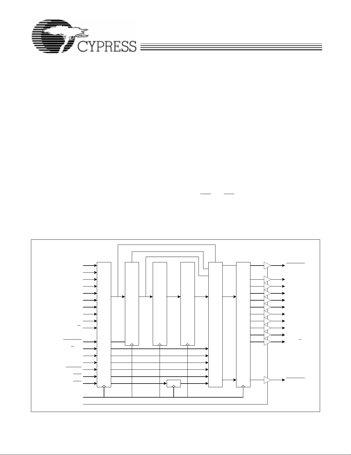
Logic Block Diagram
PD9(SVS)
PD
8
PD
7
PD
6
PD
5
PD
4
PD
3
PD
2
PD
PD0(SC/D)
1
TRS_FILT
SC/D_EN
SVS_EN
BYPASS
DVB_EN
ENA
ENN
CKW
OE
10
TRS FILTER / DETECTOR
INPUT REGISTER
10
10
10 10
NRZI ENCODER
SMPTE SCRAMBLER
MODE MULTIPLEXOR
OUTPUT REGISTER
TRS_DET
Q
(SVS)
9
Q
8
Q
7
Q
6
Q
5
Q
4
Q
3
Q
2
Q
1
Q0(SC/D)
ENA_OUT
Cypress Semiconductor Corporation
• 3901 North First Street • San Jose • CA 95134 • 408-943-2600
March 19
1999
Page 2
PRELIMINARY
HOTLink is a trademark of Cypress Semiconductor Corporation.
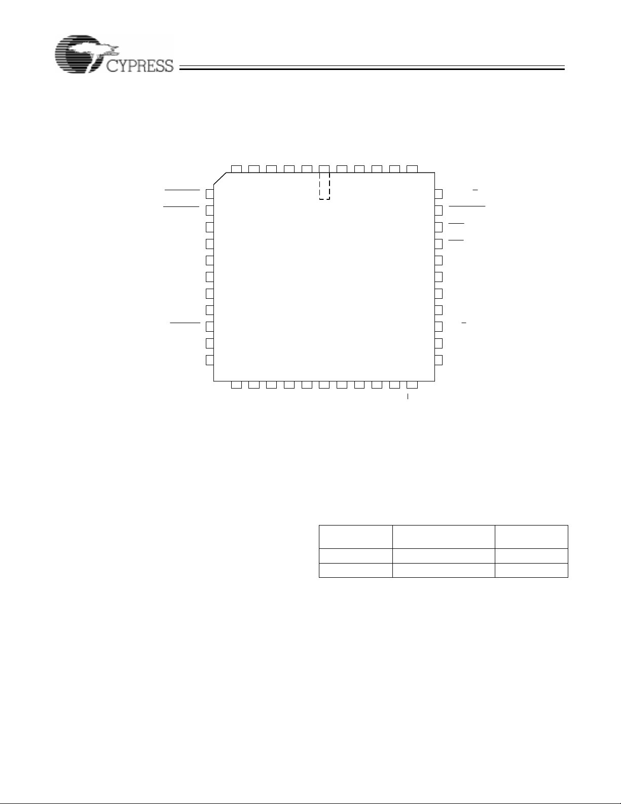
Pin Configuration
CY7C9235
Maximum Ratings
(SVS)
8
9
Q
Q
OE
NC
7
8
9
10
11
SS
12
SS
13
SS
14
15
16
17
NC
18 19 20 21 22 23 24 25 26 27 28
7
8
PD
PD
TRS_DET
TRS_FILT
SVS_EN
V
V
V
BYPASS
(SVS) NC
PD
9
5Q6Q7
V
Q
1444342414023456
PLCC
Top View
5PD6
CC
V
V
PD
CC
SS
V
SS
PD4PD3PD2PD
2Q3Q4
1
Q
Q
1
(SC/D)
0
PD
39
38
37
36
35
34
33
32
31
30
29
Q
(SC/D)
0
ENA_OUT
ENN
ENA
CKW
V
SS
V
SS
V
SS
SC/D_ENDVB_EN
NC
(Abov e which the useful lif e m ay be impaired. For user guidelines, not tested.)
Storage Temperature .....................................−40°C to +125°C
Supply Voltage to Ground Potential..................−0.5V to +7.0V
DC V oltage Applied to Outputs
in High-Z State.....................................................−0.5V to +7.0V
Output C ur re n t in to O u tp u ts.. .. ... .......... .. .......... .. ..........16 m A
DC Input Voltage.................................................−0.5V to +7.0V
Static Discharge Voltage.............................................. > 2001 V
(per MIL-STD-883, Method 3015)
DC Input Current.............................................................± 20 mA
Latch-Up Current............................................................>200 mA
Operating Range
Range
Commercial 0°C to +70°C 5V ± 5%
Industrial
Ambient
Temperature V
−40°C to +85°C
CC
5V ± 10%
2
Page 3
PRELIMINARY
CY7C9235
Pin Descriptions
CY7C9235 SMPTE-259M Encoder
Name I/O Description
ENA Input Enable Parallel Data. If ENA is LOW at th e rising edge of CKW , the data prese nt on the PD
inputs is latched , and routed to the Q
active ( LOW). If the CY7C9235 is only used in SMPTE-259M mode this signal shoul d be ti ed
to V
.
SS
outputs. This pin is only interpreted when D VB_EN is
0–9
ENN Input Enable Next Parallel Data. If ENN is LOW at the rising edge of CKW, the data present on the
PD
inputs at t he next rising edge of TXCLK is latched, and routed to the Q
0–9
pin is only interpreted when DVB_EN
SMPTE-259M mode this signal should be tied to V
is active (LO W ). If the CY7C9235 is only used in
.
SS
outputs. This
0–9
BYPASS Input Bypass SMPTE Encoding. BYP ASS is ignore d if DVB_EN is act iv e (LO W). If BYPASS is HIGH
at the rising edge of CKW (and DVB_EN
is HIGH), the data latche d int o the input register is
routed around both the SMPTE scrambler and the NRZI encoder and presented to the output
register. If BYPASS is LOW at the rising edge of the CKW clock (and DVB_EN
is HIGH), the
data present in the in put register is routed th rough the SMPTE scrambler and NRZI encoder.
TRS_DET Output TRS Character Detect ed. This output indi cat es when a c haract er used i n the TRS s equen ce is
detected in the input register . If the data cont ains any of th e reserved characte rs of 000–003 or
3FC–3FF in 10- bi t he x, t he output will be LO W f or one cl oc k peri od. I f t he c haract er i n t he in put
register is any other pattern (or DVB_EN
is LOW) this output will remain HIGH.
TRS_FILT Input TRS Character Filter. This signal c ontrols an internal filter that con verts the low-o rder two bits
of all TRS char acters to same stat e as the upper eight bi ts. This al lows a pr oper 30-bit TRS ID
to be generated when t he CY7C9235 is operated with 8-bit or non-standard video st reams.
When this sig nal i s LO W, all characters f rom 00 0–003 are con v erted to 0 00, and a ll ch ar acters
from 3FC–3FF are converted to 3FF. When TRS_FILT
is disabled (HIG H), all characters are
passed to the scr ambler wit hout modifi cation. This si gnal has no eff ect when D VB_EN
(LOW).
SVS_EN Input Send Violation Symbol Enable. This input is only valid when DVB_EN is active (LOW). If
SVS_EN is HIGH and a HI GH input is pr esen t on PD
, Q9 will also be hi gh on a followi ng cloc k
9
cycle, forcing the CY7B9234 serializer to generate an invalid 8B/10B character. If SVS_EN is
LOW, the level present on PD
is ignored and Q9 is forced to a LO W st ate.
9
SC/D_EN Input Special Character /Data Sel ect Enab le. This input is only vali d when D VB_EN is active (LOW).
If SC/D
_EN is HIGH and a HIGH input is present on PD0, Q0 will also be high on a fo llowing
clock cycl e, f orcing the CY7B923 4 serializer to generate an 8B/ 10B control char acter as sele cted by the cha r acter p rese nt on t he PD
is ignored and Q
is forced to a LO W (data only) state.
0
inputs. If SC/D_EN i s LO W, the level pr esent on PD0
8–1
PD9(SVS) Input Parallel Data 9 or Send Violat ion Symbol. This is the MSB of the input dat a fi eld. It is latched
PD
8–1
in the input register at the rising edge of CKW. When DVB_EN
is HIGH, thi s latched inpu t is rout ed to the out put register bit Q
(LOW) and SVS _EN is L O W, output register b it Q
D VB_EN
is inactive (HIGH), this latched inp ut i s routed to the scrambl er and NRZI encoder.
(SVS) is forced t o a LOW (z ero) lev el. Wh en
9
Input Parallel Data 8 through 1. The signals present at the PD
register a t the risi ng edge of CKW. When DVB_EN
is HIGH, these s ignal s are the middle ei ght
is active (LOW) and SVS_EN
(SVS). When D VB_EN is act iv e
9
inputs are latched in the input
8–1
bits of the SMPTE 10-bit dat a fi eld, and are then routed to the scr am bler and NRZI encoder.
When DVB_EN
to the Q
is activ e (LOW), these signals are full DVB-ASI data bus, and are then r outed
outputs.
8−1
PD0(SC/D) Input Paral lel Data 0 or Sp ecial Code/Dat a Select . Thi s is th e LSB of the i nput data f iel d. It is lat ched
in the input register at the rising edge of CKW. When DVB_EN
is HIGH, thi s input is rout ed to output register bi t Q
SC/D
_EN is LOW , outpu t register bit Q0 (SC/D) is f orced t o a L OW (z ero) le v e l. When DVB_EN
(SVS). When D VB_EN is activ e (LO W) and
0
is active (LOW) and SC/D _EN
is inactiv e ( HIGH), this i nput d ata bit is r out ed thr ough the i npu t regist er and the s cram ble r an d
NRZI encoder.
Q9(SVS) Output Output Bit 9. This is the MSB of the out put register . It should be connecte d dir ectly to the
CY7B9234 serializer input signal SVS(Dj).
Q
8–1
Output Output Bits 8 through 1. These signals should be connect ed directly to the CY7B9234 serializer
input signal s D
respectively.
7−0
0−9
is activ e
3
Page 4

PRELIMINARY
CY7C9235
Pin Descriptions
(continued)
CY7C9235 SMPTE-259M Encoder
Name I/O Description
Q0(SC/D) Output Output Bit 0. This is the LSB of the output register. It should be connected directly to the
CY7B9234 serializer input signal SC/D
(Da).
DV B_EN Input DVB Mode Enable. This signal is sampled by the risi ng edge of the CKW clock. If DVB_EN is
active (LOW), the data present on t he PD
the Q
and ENA_OUT outputs.
0−9
, ENA, and ENN inputs are latched a nd routed to
0−9
CKW Input Clock Writ e. This clock c ontrols all synch ronous oper ations of the CY 7C9235. It operates at the
character rate which is equivalent to one t enth the serialized bit-r ate. This clock also connects
directly to the CKW input of the CY7B9234 serializer.
ENA_OUT Output Enable Parallel Data Out. This output attached directl y to the CY7B9234 ENA input, and iden-
tifies when val id data is a vailab le at the CY7C9235 output s. If used onl y for SMPTE-2 59M data
streams, this output may be left open, with the ENA
to V
.
SS
input to the CY7B9234 direct ly connect ed
OE Input Output Enabl e. When th is signal is HI GH all outputs are d riven to th eir normal logic l evels . When
LOW, all outputs are placed in a High-Z state.
V
CC
V
SS
Power.
Ground.
CY7C9235 Description
Input Register
The input register is clocked by the rising edge of CKW. This
register captur es the data present at the PD
clock cycle. In addition to the data inputs, all control inputs
inputs on e v ery
0−9
except O E are al so c apture d at each ri sing edge of CKW. This
includes BYPASS, DVB_EN
TRS_FILT
, ENN, and ENA.
, SVS_EN, SC/D_EN, TRS_DET,
TRS Filter
The TRS Filter is used to convert all 8-bit TRS characters
(000–003 and 3FC–3FF in 10 -bit hex) to their ful l 10-bit v alue.
If TRS_FILT
is active (LOW) and any of these values are detected in the input register, the lower two bits are forced to
either zeros or ones respectively. This allows the encoder to
be used with both 8- and 10-bit SMPTE character streams.
If TRS_FIL T
is HIGH, the f ilter func tion is d isable d and all cha racters are passed fr om the input regist er to t he SMPTE scr ambler unmodified.
TRS Detector
When operated in SMPTE mode (DVB_EN
is HIGH), the TRS
detector looks for the most significant eight bits of the input
register to be either all ones or all zeros. If either of these
values are detected, the TRS_DET
output will go LOW following the rising edge of CKW, and remain LO W until a charact er
is detecte d in the input r egister that is not all zeros or ones, or
D VB_EN
is latched LOW.
SMPTE Scrambler
The SMPTE scrambl er implements a paral lel encoded vers ion
of a linear-feedback shift register. It encodes the data present
in the input register using the X
9
+ X4 + 1 poly nomial t o increase the transition density of the serial data stream and to
decrease the DC-cont ent of the transmitted serial bit stream.
NRZI Encoder
The scrambled data is also fed through an NRZ-to-NRZI encoder. This also increases the transition density of the serial
data stream, decr eases the DC-content of the transmitted serial bit stream, and makes the serial stream insensitive to polarity inve rs ions.
DVB-ASI Operation
The CY7C9235 is designed to operate in both SMPTE-259M
and DVB-ASI environments. When operated in SMPTE-only
environments , the D VB contr ol input s ma y be tie d to eit her V
or VSS as needed to place them in a known state. When not
used for DVB operation, the ENA
SC/D
_EN inputs many be tied to either VCC or VSS. DVB_EN
, ENN, SVS_EN, and
must be tied or driven HIGH.
DVB-ASI operation is enabled by asserting DVB_EN
LOW.
This signal is latched by the rising edge of the CKW clock.
When the CY7C9235 is placed in DVB mode, t he SMPTE and
NRZI encoders are bypassed, and the data latched into the
input register is routed directly to the output register.
Error Propagation
For those DVB-ASI implementations that do not require propagation of detected errors, the Q
zero by setting SVS_EN LOW. When SVS_EN is HIGH (and
the encoder is in DVB mode) the PD
input register is routed to the output register and to the
output may be forced to a
9
data latched into the
9
CY7B9234 SVS input.
Command Code Generatio n
The DVB-ASI interface does not normally transmit any com-
mand characters other than the K28.5 code that is used both
for synchr onization and as a fill charac ter when data is not
being transmitted. These K28.5 characters may be generat ed
by two methods; by con trolling when the CY7C9235 is enab led
CC
4
Page 5

PRELIMINARY
CY7C9235
using the ENA
on the PD
and ENN inpu ts, or b y pl acing a C5.0 c har acter
inputs when one of the two enables is active .
9–0
If the generation of K28.5 fill characters is to be controlled
using the ENA
driven LOW or connect ed to V
Electrical Characteristics
or EN N inputs, the SC/D_EN input should be
. This will insure that the PD
SS
Over the Ope rating Range
data bit is not routed to the output register by forcing the Q
output to always be LOW.
If the generation of a K28.5 characters is controlled by transmission of a C5. 0 charact er, the SC/D
to allow the PD
0
input to be propagated to the Q0 output.
0
_EN input must be HIGH
Parameter Description Tes t Condi tions Min. Max. Unit
V
OH
V
OL
V
IH
V
IL
I
IX
I
OZ
I
OS
I
CC
Capacitance
Output HIGH Voltage VCC=Min., IOH = −3.2 mA 2.4 V
Output LOW Voltage VCC=Min., IOL = 16.0 mA 0.5 V
Input HIGH Voltage Guaranteed Input Logical HIGH
V oltage for al l In puts
Input LOW Voltage Guaranteed Input Logical HIGH
Voltage fo r al l Inputs
Input Load Current VI = VCC or V
Output Leakage Current VO = VCC or V
Output Short Circuit Current
Power Supply Current VIN, V
[3]
[2,3]
VCC = Max., V
= VCC or V
I/O
SS
SS
OUT
[1]
[1]
= 0.5V
SS
2.0 7.0 V
–0.5 0.8 V
−10
−50
+10
+50
−10 −80
Parameter Description Test Conditions Max. Unit
C
IN
C
OUT
Notes:
1. These are absolute values with respect to device ground. All overshoots due to system or tester noise are included.
2. Not more than one output should be tested at a time. Duration of the short circuit should not exceed 1 second. V
problems caused by tester ground degradation.
3. Tested initially and after any design or process changes that may affect these parameters.
Input Capacitance VIN = 5.0V at f = 1 MHz 10 pF
Output Capacitance V
= 5.0V at f = 1 MHz 12 pF
OUT
= 0.5V has been chosen to avoid test
OUT
0
µA
µA
mA
mA
5
Page 6

PRELIMINARY
AC Test Loads and Waveforms
TTL OUT PUTS
5V
OUTPUT
INCLUDING
JIG AND
SCOPE
35 pF
238
(a)
Ω
5V
OUTPUT
170
Ω
5 pF
INCLUDING
JIG AND
SCOPE
Equivalent to: THÉVENIN EQUIVALENT
OUTPUT
Switching Characteristics
Over the Operating Range
Parameter Description
t
SD
t
HD
t
CPWH
t
CPWL
t
CKW
t
A
t
H
t
EA
t
ER
Notes:
4. All AC parameters are with all outputs switching.
5. Test load (b) used for this parameter. Test load (a) used for all other AC parameters.
Data Set-Up Time 10 8 ns
Data Hold Time 0 0 ns
CKW Pulse Width HIGH 6.5 6.5 ns
CPW Pulse Width LOW 6.5 6.5 ns
Write Clock Period 30 62.5 25 62.5 ns
Access Time 10 8 ns
Data Output Hold Time From CKW Rise 4 3 ns
Input to Output Enab le 23 20 ns
Input to Output Disable
[5]
238
(b)
Ω
99
Ω
[4]
170
CY7C9235
3.0V
GND
<2ns <2ns
2.08V
CY7C9235-27 CY7C9235-40
ALL INPUT PULSES
90%
10%
23 20 ns
90%
10%
7C9335–9
UnitMin. Max. Min. Max.
Switching Waveform
PD
, ENA, ENN,
0−9
BYPASS, TRS_FILT ,
SVS_EN, SC/D
Q
0–9
_EN,
DVB_EN
CKW
, TRS_DET,
ENA_OUT
OE
t
CKW
t
SD
t
CPWL
t
t
ER
EA
t
HD
t
CPWH
t
A
t
H
6
Page 7

PRELIMINARY
v
Ordering Information
Ordering Code
Name Package Type
CY7C9235-270JC J67 44-pin Pl astic Leaded Chip Carrier Commercial
CY7C9235-400JC J67 44-pin Pl astic Leaded Chip Carrier Commercial
Document #: 38-00571-A
Package Diagram
44-Lead Plastic Leaded Chip Carrier J67
Package
Operating
Range
CY7C9235
51-85003-A
© Cypress Semiconductor Corporation, 1999. The information contained herein is subject to change without notice. Cypress Semiconductor Corporation assumes no responsibility for the use
of any circuitry other than circuitry embodied in a Cypress Semiconductor product. Nor does it convey or imply any lice nse under patent or other rights. Cypress Semi conductor does not authorize
its products for use as critical components in life-support systems where a malfunction or failure may reasonably be expected to result in significant injury to the user. The inclusion of Cypress
Semiconductor products in life-support systems application implies that the manufacturer assumes all risk of such use and in doing so indemnifies Cypress Semiconductor against all charges.
 Loading...