

Page 1

CY7C63722
CY7C63723
CY7C63743
enCoRe™ USB Combination Low-Speed
USB and PS/2 Peripheral Controller
1.0 Features
• enCoRe™ USB - enhanced Component Reduction
—Internal oscillator e liminates the need for an external
crystal or resonator
—Interface can auto-configure to operate as PS/2 or
USB without the need for external components to
switch between modes (no General Purpose I/O
[GPIO] pins needed to manage dual mode cap ability)
—Internal 3.3V regulator for USB pull-up resistor
—Configurable GPIO for real-world interface without
external components
• Flexible, cost-effective solution for applications that
combine PS/2 and low-speed USB, such as mice, gamepads, joysticks, and many others.
• USB Specification Compliance
—Conforms to USB Specification, Version 2.0
—Conforms to USB HID Specification, Version 1.1
—Supports one low-speed USB device address and
three data endpoints
—Integrated USB transceiver
—3.3V regulated output for USB pull-up resistor
• 8-bit RISC microcontroller
—Harvard architecture
—6-MHz external ceramic resonator or internal clock
mode
—12-MHz internal CPU clock
—Internal memory
—256 bytes of RAM
—8 Kbytes of EPROM
—Interface can auto-configure to operate as PS/2 or
USB
—No external componen ts for switching betw een PS/2
and USB modes
—No GPIO pins needed to manage dual mode
capability
• I/O ports
—Up to 16 versatile GPIO pins, individually
configurable
—High current drive on any GPIO pin: 50 mA/pin
current sink
—Each GPIO pin supports high-impedance inputs,
internal pull-ups, open drain outputs or traditional
CMOS outputs
—Maskable interrupts on all I/O pins
• SPI serial communication block
—Master or slave operation
—2 Mbit/s transfers
• Four 8-bit Input Capture registers
—Two registers each for two input pins
—Capture timer setting with five prescaler settings
—Separate registers fo r rising and falling edge capture
—Simplifies interface to RF inputs for wireless
applications
• Internal low-power wake-up timer during suspend
mode
—Periodic wake-up with no external components
• Optional 6-MHz internal oscillator mode
—Allows fast start-up from suspend mode
• Watchdog Reset (WDR)
• Low-voltage Reset at 3.75V
• Internal brown-out reset for suspend mode
• Improved output drivers to reduce EMI
• Operating voltage from 4.0V to 5.5VDC
• Operating temperature from 0°C to 70°C
• CY7C63723 available in 18-pin SOIC, 18-pin PDIP
• CY7C63743 available in 24-pin SOIC, 24-pin PDIP , 24-pin
QSOP
• CY7C63722 available in DIE form
• Industry standard programmer support
Cypress Semiconductor Corporation • 3901 North First Street • San Jose • CA 95134 • 408-943-2600
Document #: 38-08022 Rev. *B Revised September 27, 2004
Page 2
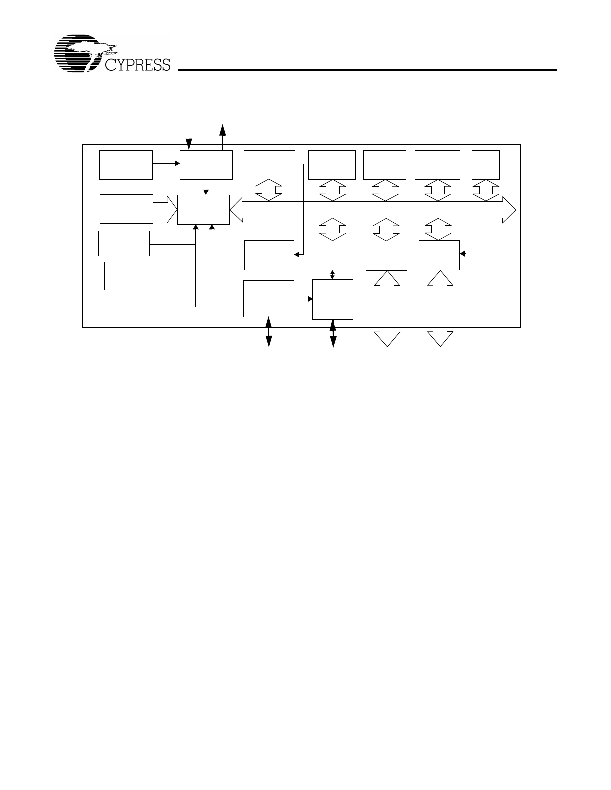
2.0 Logic Block Diagram
FOR
FOR
CY7C63722
CY7C63723
CY7C63743
XTALOUT XTALIN/P2.1
Internal
Oscillator
EPROM
8K Byte
Brown-out
Reset
Xtal
Oscillator
8-bit
RISC
Core
Wake-Up
Timer
Interrupt
Controller
Watch
Dog
Timer
Low
Voltage
Reset
3.3V
Regulator
VREG/P2.0
3.0 Functional Overview
3.1 enCoRe USB—The New USB Standard
Cypress has reinvented its leadership position in the
low-speed USB market with a new family of innovative
microcontrollers. Introducing...enCoRe USB—“enhanced
Component Reduction.” Cypress has leveraged its design
expertise in USB solutions to create a new family of low-speed
USB microcontrollers that enables peripheral developers to
design new prod ucts with a minimum number of compone nt s .
At the heart of the enCoRe USB technology is the breakthrough de sign of a crystalless os cillator. By integrating t he
oscillator into our chip, an external crystal or resonator is no
longer needed. We have also integrated other extern al components common ly found in low-sp eed USB applica tions such as
pull-up resistors , wake-up ci rcuitry, and a 3.3V regul ator. All of
this adds up to a lower system cost.
The CY7C637xx is an 8-bit RISC one-time-programmable
(OTP) microcontroller. The instructi on set has been opt imize d
specifically for USB and PS/2 operati ons , alt hou gh the mic rocontrollers can b e us ed fo r a v ari ety o f other embedded a ppl ications.
The CY7C637xx features up to 16 G PIO pins to support USB,
PS/2 and other applications . The I/O pins are grouped into two
ports (Port 0 to 1) where each pin can be individually
configured as input s with internal p ull-up s, open drai n output s,
or traditional CMOS output s with programm able drive strength
of up to 50 mA output drive. Additionally, each I/O pin can be
used to generate a GPIO i nter rupt to the mi croco ntrolle r. Note
the GPIO interrupts all share the same “GPIO” interrup t vector .
The CY7C637xx mic rocontrollers fe ature an interna l oscillator .
With the presence of USB traf fic, the int erna l oscilla tor can be
set to precisely tune to USB timing requirements (6 MHz
RAM
256 Byte
USB
Engine
12-bit
Timer
Port 1
GPIO
Capture
Timers
Port 0
GPIO
SPI
USB &
PS/2
Xcvr
D+,D–
±1.5%). Optionally, an external 6-MHz ceramic resonator can
be used to provide a higher precision reference for USB
operation. This clock generator reduces the clock-related
noise emissions (EMI). The clock generator provides the 6and 12-MHz clocks that rem ain internal to the mic rocontroller .
The CY7C637xx has 8 Kbytes of EPROM and 256 bytes of
data RAM for stack space, user variables, and USB FIFOs.
These parts i nclude low- voltage re set logic, a W atchd og timer ,
a vectored interrupt controll er, a 12-bit free-runnin g timer, and
capture timers. The low-voltage reset (LVR) logic detects
when power is applied to the device, resets the logic to a
known state, and begins executing instructions at EPROM
address 0x0000. LVR will also reset the part when V
below the operating voltage range. The Watchdog timer can
be used to ensure the firmware never gets stalled for more
than approximately 8 ms.
The microcontroller supports 10 maskable interrupts in the
vectored interrupt c ontroller . Interrupt sour ces include the U SB
Bus-Reset, the 128-µs and 1.024-ms outputs from the
free-running timer, three USB endpoints, two capture timers,
an internal wake-up tim er and th e G PIO p ort s . The timers bits
cause periodic interrupts when enabled. The USB endpoints
interrupt after USB transactions complete on the bus. The
capture timers interrupt whenever a new timer value is saved
due to a selected GPIO edge event. The GPIO ports have a
level of masking to select which GPIO inputs can cause a
GPIO interrupt. For additional flexibility, the input transition
polarity that causes an interrupt is programmable for each
GPIO pin. The interrupt polarity can be either rising or falling
edge.
The free-running 12-bit timer clocked at 1 MHz provides two
interrupt sources a s no ted above (128 µs and 1.024 ms ). Th e
timer can be used to measure the duration of an event under
firmware control by read ing the timer at the start and end of an
P1.0–P1.7
P0.0–P0.7
CC
drops
Document #: 38-08022 Rev. *B Page 2 of 49
Page 3
FOR
FOR
CY7C63722
CY7C63723
CY7C63743
event, and subtracti ng the two values. T he four capture ti mers
save a programmable 8 bit range of the free-running timer
when a GPIO edge occurs on the two capture pins (P0.0,
P0.1).
The CY7C637xx includes an integrated USB serial interface
engine (SIE) that supports the integrated peripherals. The
hardware supports one USB device address with three
endpoints. The SIE al low s the USB hos t to c ommun ic ate with
the function integrated into the microcontroller. A 3.3V
The USB D+ and D– USB pins c an alternately be used a s PS/2
SCLK and SDATA signals, so that products can be designed
to respond to either USB or PS/2 modes of operation. PS/2
operation is suppo rted with i nte rnal pu ll-u p res is tors on SC LK
and SDAT A, the abil ity to di sable the regul ator outp ut pin, an d
an interrupt to signal the start of PS/2 activity. No external
components are necessary for dual USB and PS/2 systems,
and no GPIO pins need to b e dedicated to switching b etween
modes. Slow edge rates operate in both modes to reduce EM I.
regulated output pin provides a pull-up source for the external
USB resistor on the D– pin.
4.0 Pin Configurations
Top View
CY7C63723
18-pin SOIC/PDIP
P0.0
1
P0.1
2
P0.2
3
P0.3
4
P1.0
5
6
VSS
7
VPP
VREG/P2.0
XTALIN/P2.1
8
9
18
17
16
15
14
13
12
11
10
P0.4
P0.5
P0.6
P0.7
P1.1
D+/SCLK
D–/SDATA
VCC
XTALOUT
CY7C63743
24-pin SOIC/PDIP/QSOP
P0.0
1
P0.1
P0.2
P0.3
P1.0
P1.2
P1.4
P1.6
VSS
VPP
VREG/P2.0
XTALIN/P2.1
24
23
2
22
3
21
4
20
5
19
6
18
7
17
8
16
9
15
10
14
11
13
12
P0.4
P0.5
P0.6
P0.7
P1.1
P1.3
P1.5
P1.7
D+/SCLK
D–/SDATA
VCC
XTALOUT
CY7C63722-XC
3 P0.2
2 P0.1
P0.3
4
P1.0
5
6
P1.2
P1.4
7
P1.6
8
9
VSS
VSS
10
111213
VPP
VREG
DIE
1 P0.0
25 P0.4
24 P0.5
23 P0.6
22
P0.7
21
P1.1
20
P1.3
19
P1.5
18
P1.7
17
D+/SCLK
15
16
14
VCC
D-/SDATA
XTALOUT
XTALIN/P2.1
5.0 Pin Definitions
CY7C63723 CY7C63743 CY7C63722
Name I/O
D–/SDATA,
D+/SCLK
P0[7:0] I/O 1, 2, 3, 4,
I/O 12
13
15, 16, 17, 18
15
16
1, 2, 3, 4,
21, 22, 23, 24
16
17
1, 2, 3, 4,
22, 23, 24, 25
USB differential data lines (D– and D+), or PS/2 clock
and data signals (SDATA and SCLK)
GPIO Port 0 capable of sinking up to 50 mA/pin, or
sinking controlled low or high programmable current.
Can also source 2 mA current, provide a resistive
pull-up, or serve as a high-impedance input. P0.0 and
P0.1 provide inputs to Capture Timers A and B, respectively.
P1[7:0] I/O 5, 14 5, 6, 7, 8,
17, 18, 19, 20
5, 6, 7, 8,
18, 19, 20, 21
IO Port 1 capable of sinking up to 50 mA/pin, or sinking
controlled low or high programma ble c urrent. Can also
source 2 mA current, provide a resistive pull-up, or
serve as a high-impedance input.
XTALIN/P2.1 IN 9 12 13 6-MHz ceramic resonator or external clock input, or
P2.1 input
XT ALOUT OUT 10 13 14 6-MHz ceramic resonator return pi n or internal oscillator
output
V
PP
V
CC
7 10 11 Programming voltage supply, ground for normal
operation
11 14 15 Voltage supply
VREG/P2.0 8 11 12 Voltage supply for 1.3-kΩ USB pull-up resistor (3.3V
nominal). Also serves as P2.0 input.
V
SS
6 9 9, 10 Ground
Description18-Pin 24-Pin 25-Pad
Document #: 38-08022 Rev. *B Page 3 of 49
Page 4

FOR
FOR
CY7C63722
CY7C63723
CY7C63743
6.0 Programming Model
Refer to the CYASM Assembler User’s Guide for more deta ils
on firmware operation with the CY7C637xx microcontrollers.
6.1 Program Counter (PC)
The 14-bit program counter (PC) allows access for up to 8
Kbytes of EPROM using the CY7C637xx architecture. The
program counter is cleared during reset, such that the first
instruction executed after a reset is at address 0x0000. This
instruction is typica lly a jump inst ruction to a reset h andler that
initializes the appli cat ion.
The lower 8 bits of the program counter are incremented as
instructions are l oaded and exec uted. The upper six bit s of the
program counter are incremented by executing an XPAGE
instruction. As a result, th e last instr uction exec uted within a
256-byte “page” of sequential code should be an XPAGE
instruction. The assembler directive “XPAGEON” will cause
the assembler to insert XPAGE instructions automatically. As
instructions can be eit her one or two bytes long, the assembl er
may occasionally need to inser t a NOP followe d by an XP AGE
for correct execution.
The program counter of the next instruction to be executed,
carry flag, and zero flag are saved as two bytes on the progra m
stack during an interrupt acknowledge or a CALL instruction.
The program counter, carry flag, and zero flag are restored
from the program stack only during a RETI instruction.
Please note the program counte r cannot be acces sed directl y
by the firmware. The program stack can be examined by
reading SRAM from location 0x00 and up.
6.2 8-bit Accumulator (A)
The accumulator is the general-purpose, do everything
register in the architecture where results are usually calculated.
6.3 8-bit Index Register (X)
The index register “X” is available to the firmware as an
auxiliary accumu lator . The X register also allows the proce ssor
to perform indexed operations by loading an index value
into X.
The return from interrupt (RETI) instruction decrements the
program stack pointer, then restores the second byte from
memory addressed by the PSP. The program stack pointer is
decremented again and th e first byte is restored from mem ory
addressed by the PSP. After the program counter and flags
have been restored from st ack, the interrupt s are enabled. The
effect is to restore the program counter and flags from the
program stack, decrement the program stack pointer by two,
and reenable interrupts.
The call subroutine (CALL) instruction stores the program
counter and flags on the program stack and increments the
PSP by two.
The return from subroutine (RET) instruction restores the
program counter, but not the flags, from program stack and
decrements the PSP by two.
Note that there are restrictions in using the JMP, CALL, and
INDEX instructions across the 4-KByte boundary of the
program memory. Refer to the CYASM Assembler User’s
Guide for a detailed description.
6.5 8-bit Data Stack Pointer (DSP)
The data stack pointer (DSP) supports PUSH and POP
instructions that use the data stack for temporary storage. A
PUSH instruction will pre-decrement the DSP, then write data
to the memory location addressed by the DSP. A POP
instruction will read dat a from the me mory lo catio n addres sed
by the DSP, then post-increment the DSP.
During a reset, the Data Stack Pointer will be set to zero. A
PUSH instruction when DSP equ als ze ro will wri te da t a at th e
top of the data RAM (address 0xFF). This would write data to
the memory area re serv ed f or a FIF O f or U SB e ndpoi nt 0. In
non-USB applications, this works fine and is not a problem.
For USB applications, the firmware should set the DSP to an
appropriate location to avoid a memory conflict with RAM
dedicated to USB FIFOs. The memory requirements for the
USB endpoints are shown in Section 8.2. For example,
assembly instructions to set the DSP to 20h (giving 32 bytes
for program and data stack combined) are shown below.
MOV A,20h ; Move 20 hex into Accumu lator (must be
D8h or less to avoid USB FIFOs)
SWAP A,DSP ; swap acc umula tor value in to DSP reg ist er
6.4 8-bit Program Stack Pointer (PSP)
During a reset, the progra m sta ck point er (PSP) is set to zero.
This means the program “stack” starts at RAM address 0x00
and “grows” upward from there. Note that the program stack
pointer is directly addressable under firmware control, using
the MOV PSP,A instruction. The PSP supports interrupt
service under hardware control and CALL, RET, and RETI
instructions under firmware control.
During an interrupt acknowledge, interrupts are disabled and
the program counter, carry flag, and zero flag are written as
two bytes of data memory. The first byte is stored in the
memory addressed by the program stack pointer, then the
PSP is incremented. The second byte is stored in memory
addressed by the progra m st ack poi nter and the PS P is inc remented again. The net effect is to store the program counter
and flags on the program “stack” and increment the program
stack pointer by two.
Document #: 38-08022 Rev. *B Page 4 of 49
6.6 Address Modes
The CY7C637xx microcontrollers support three addressing
modes for instructions that require dat a operands: dat a, direct,
and indexed.
6.6.1 Data
The “Data” address mode refers to a data operand that is
actually a const ant en coded in t he instruc tion. As an example,
consider the instruction that loads A with the constant 0x30:
• MOV A, 30h
This instruction will require two bytes of code where the first
byte identifies the “MOV A” inst ruc tion w ith a d at a operand as
the second byte. Th e second byte of the instru ction will b e the
constant “0xE8h”. A constant may be referred to by name if a
prior “EQU” statement a ssigns the co nstant valu e to the name.
For example, the following code is equivalent to the example
shown above.
Page 5

FOR
FOR
CY7C63722
CY7C63723
CY7C63743
• DSPINIT: EQU 30h
• MOV A,DSPINIT
6.6.2 Direct
“Direct” address mode is used when the data operand is a
variable stored in SRAM. In that cas e, the one byte address of
the variable is encoded in the instruction. As an example,
consider an instruction that loads A with the contents of
memory address location 0x10h:
• MOV A, [10h]
In normal usage, variable names are assigned to variable
addresses using “EQU” statements to improve the readability
of the assembler source code. As an example, the following
code is equivalent to the example shown above.
• buttons: EQU 10h
• MOV A, [buttons]
6.6.3 Indexed
“Indexed” address mode allows the firmware to manipulate
arrays of data stored in SRAM. The address of the data
operand is the sum of a constant encoded in the instruction
and the contents of the “X” register. In normal usage, the
constant will be the “base” address of an array of data and the
X register will cont ain an index th at indica tes which element of
the array is actually addressed.
• array: EQU 10h
• MOV X,3
• MOV A, [x+array]
This would have the effect of loading A with the fourth element
of the SRAM “array” that begins at addr ess 0x 10h . The fourth
element would be at address 0x13h.
7.0 Instruction Set Summary
Refer to the CYASM Assembler User’s Guide for detailed
information on these instructions. Note that conditional jump
instructions (i.e., JC, JNC, JZ, JNZ) take five cycles if jump is
taken, four cycles if no jump.
MNEMONIC Operand Opcode Cycles
HALT 00 7
ADD A,expr data 01 4 INC A acc 21 4
ADD A,[expr] direct 02 6
ADD A,[X+expr] index 03 7
ADC A,expr data 04 4 INC [X+expr] index 24 8
ADC A,[expr] direct 05 6
ADC A,[X+expr] index 06 7
SUB A,expr data 07 4 DEC [expr] direct 27 7
SUB A,[expr] direct 08 6
SUB A,[X+expr] index 09 7
SBB A,expr data 0A 4 IOWR expr address 2A 5
SBB A,[expr] direct 0B 6
SBB A,[X+expr] index 0C 7 POP X 2C 4
OR A,expr data 0D 4 PUSH A 2D 5
OR A,[expr] direct 0E 6
OR A,[X+expr] index 0F 7 SWAP A,X 2F 5
AND A,expr data 10 4 SWAP A,DSP 30 5
AND A,[expr] direct 11 6
AND A,[X+expr] index 12 7 MOV [X+expr],A index 32 6
XOR A,expr data 13 4 OR [expr],A direct 33 7
XOR A,[expr] direct 14 6
XOR A,[X+expr] index 15 7 AND [expr],A direct 35 7
CMP A,expr data 16 5 AND [X+expr],A index 36 8
CMP A,[expr] direct 17 7
CMP A,[X+expr] index 18 8 XOR [X+expr],A index 38 8
MOV A,expr data 19 4 IOWX [X+expr] index 39 6
MNEMONIC Operand Opcode Cycles
NOP 20 4
INC X x 22 4
INC [expr] direct 23 7
DEC A acc 25 4
DEC X x 26 4
DEC [X+expr] index 28 8
IORD expr address 29 5
POP A 2B 4
PUSH X 2E 5
MOV [expr],A direct 31 5
OR [X+expr],A index 34 8
XOR [expr],A direct 37 7
Document #: 38-08022 Rev. *B Page 5 of 49
Page 6

FOR
FOR
CY7C63722
CY7C63723
CY7C63743
MNEMONIC Operand Opcode Cycles
MOV A,[expr] direct 1A 5
MOV A,[X+expr] index 1B 6
MOV X,expr data 1C 4
MOV X,[expr] direct 1D 5
reserved 1E
XPAGE 1F 4
MOV A,X 40 4
MOV X,A 41 4
MOV PSP,A 60 4
CALL addr 50 - 5F 10
JMP addr 80-8F 5
CALL addr 90-9F 10
JZ addr A0-AF 5 (or 4) JACC addr E0-EF 7
JNZ addr B0-BF 5 (or 4)
MNEMONIC Operand Opcode Cycles
CPL 3A 4
ASL 3B 4
ASR 3C 4
RLC 3D 4
RRC 3E 4
RET 3F 8
DI 70 4
EI 72 4
RETI 73 8
JC addr C0-CF 5 (or 4)
JNC addr D0-DF 5 (or 4)
INDEX addr F0-FF 14
Document #: 38-08022 Rev. *B Page 6 of 49
Page 7
8.0 Memory Organization
FOR
FOR
CY7C63722
CY7C63723
CY7C63743
8.1 Program Memory Organization
After reset Address
14 -bit PC 0x0000 Program execution begins here after a reset
[1]
0x0002 USB Bus Reset interrupt vector
0x0004 128-µs timer interrupt vector
0x0006 1.024-ms timer interrupt vector
0x0008 USB endpoint 0 interrupt vecto r
0x000A USB endpoint 1 interrupt ve ctor
0x000C US B endpoint 2 in terrupt vector
0x000E SPI interrupt vector
0x0010 Capture timer A interrupt Vector
0x0012 Capture timer B interrupt vector
0x0014 GPIO interrupt vector
0x0016 Wake-up interrupt vector
0x0018 Program Memory begins here
0x1FDF 8 KB PROM ends here (8K - 32 bytes). See Note below
Figure 8-1. Program Memory Space with Interrupt Vector Ta ble
Note:
1. The upper 32 bytes of the 8K PROM are reserved. Therefore, the user’s program mus t not overwr i te this spac e.
Document #: 38-08022 Rev. *B Page 7 of 49
Page 8
FOR
FOR
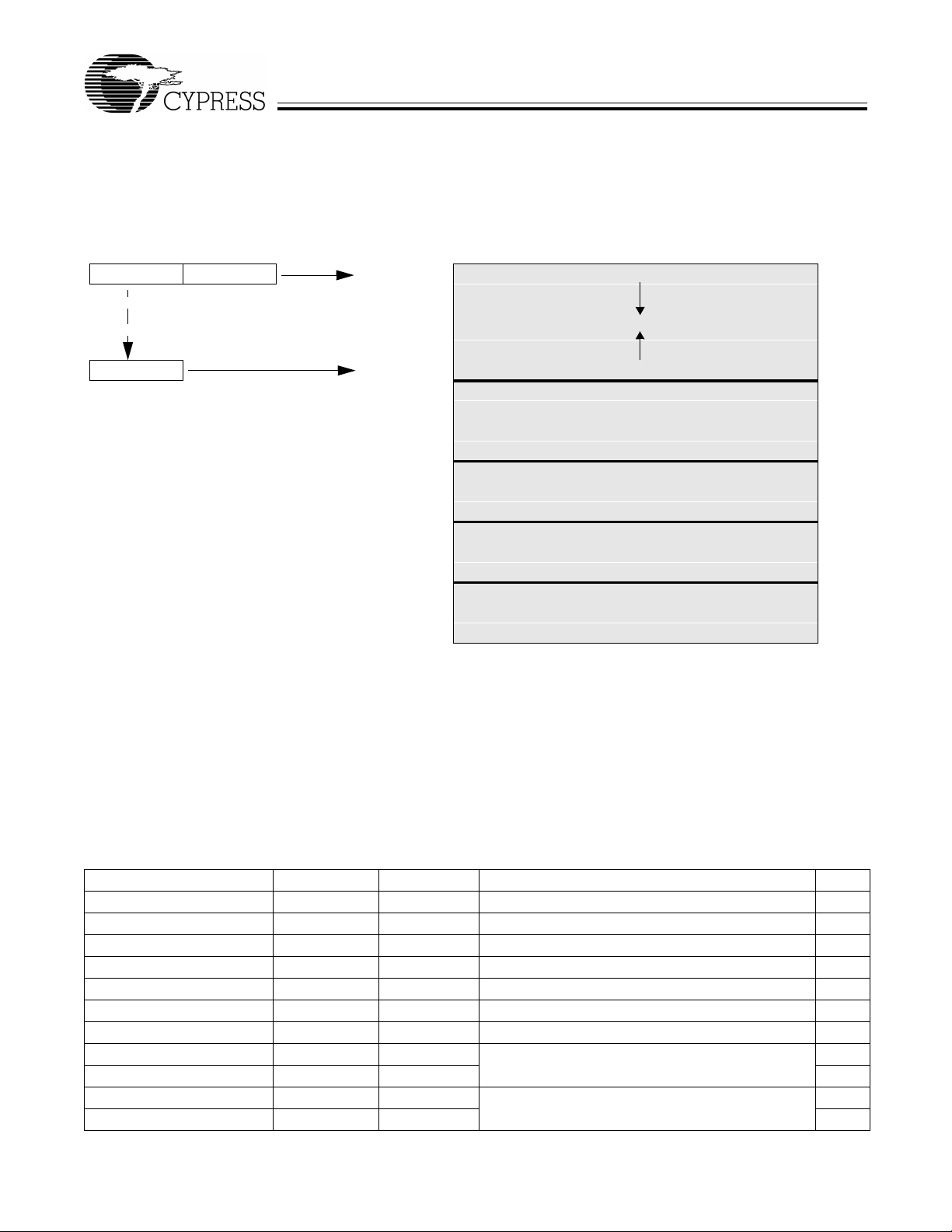
8.2 Data Memory Organization
The CY7C637xx microcontrollers provide 256 bytes of data
RAM. In normal usage, the SRAM is partitioned into four
areas: program stack, data stack, user variables and USB
endpoint FIFOs as shown below.
After reset Address
8-bit DSP 8-bit PSP 0x00 Program Stack Growth
(User’s firmware moves DSP)
8-bit DSP User Selected Data Stack Growth
User Variables
0xE8
USB FIFO for Address A endpoint 2
CY7C63722
CY7C63723
CY7C63743
0xF0
USB FIFO for Address A endpoint 1
0xF8
USB FIFO for Address A endpoint 0
Top of RAM Memory 0xFF
Figure 8-2. Data Memory Organization
8.3 I/O Register Summary
I/O registers are accessed via the I/O Read (IORD) and I/O
Write (IOWR, IOWX) instructions. IORD reads the selected
port into the accumul ator . IO WR writes data fro m the accum ulator to the selected port. Indexed I/O Write (IOWX) adds the
contents of X to the address in the instru cti on to form the port
address and writes dat a fr om the accu mulato r to the spec ified
Table 8-1. I/O Register Summary
Register Name I/O Address Read/Write Function Fig.
Port 0 Data 0x00 R/W GPIO Port 0 12-2
Port 1 Data 0x01 R/W GPIO Port 1 12-3
Port 2 Data 0x02 R Auxiliary input register for D+, D–, VREG, XTALIN 12-8
Port 0 Interrupt Enable 0x04 W Interrupt enable for pins in Port 0 21-4
Port 1 Interrupt Enable 0x05 W Interrupt enable for pins in Port 1 21-5
Port 0 Interrupt Polarity 0x06 W Interrupt polarity for pins in Port 0 21-6
Port 1 Interrupt Polarity 0x07 W Interrupt polarity for pins in Port 1 21-7
Port 0 Mode0 0x0A W Controls output configuration for Port 0 12-4
Port 0 Mode1 0x0B W 12-5
Port 1 Mode0 0x0C W Controls output configuration for Port 1 12-6
Port 1 Mode1 0x0D W 12-7
port. Note that specifying address 0 with IOWX (e.g., IOWX
0h) means the I/O port is selected solely by the contents of X.
Note: All bits of all registers are cleared to all zeros on
reset, except the Processor Status and Control Register
(Figure 20-1). All register s not liste d are reserved , and shoul d
never be written by firmware. All bits marked as reserved
should always be writte n as 0 and be tre ate d as unde fin ed by
reads.
Document #: 38-08022 Rev. *B Page 8 of 49
Page 9

FOR
FOR
CY7C63722
CY7C63723
CY7C63743
Table 8-1. I/O Register Summary (continued)
Register Name I/O Address Read/Write Function Fig.
USB Device Address 0x10 R/W USB Device Address register 14-1
EP0 Counter Register 0x11 R/W USB Endpoint 0 counter register 14-4
EP0 Mode Register 0x12 R/W USB Endpoint 0 configuration register 14-2
EP1 Counter Register 0x13 R/W USB Endpoint 1 counter register 14-4
EP1 Mode Register 0x14 R/W USB Endpoint 1 configuration register 14-3
EP2 Counter Register 0x15 R/W USB Endpoint 2 counter register 14-4
EP2 Mode Register 0x16 R/W USB Endpoint 2 configuration register 14-3
USB Status & Control 0x1F R/W USB status and control register 13-1
Global Interrupt Enable 0x20 R/W Global interrupt enable register 21-1
Endpoint Interrupt Enable 0x21 R/W USB endpoint interrupt enables 21-2
Timer (LSB) 0x24 R Lower 8 bits of free-running timer (1 MHz) 18-1
Timer (MSB) 0x25 R Upper 4 bits of free-running timer 18-2
WDR Clear 0x26 W Watchdog Reset clear -
Capture Timer A Rising 0x40 R Rising edge Capture Timer A data register 19-2
Capture Timer A Falling 0x41 R Falling edge Capture Timer A data register 19-3
Capture Timer B Rising 0x42 R Rising edge Capture Timer B data register 19-4
Capture Timer B Falling 0x43 R Falling edge Capture Timer B data register 19-5
Capture TImer Configuration 0x44 R/W Capture Timer configuration register 19-7
Capture Timer Status 0x45 R Capture Timer status register 19-6
SPI Data 0x60 R/W SPI read and write data register 17-2
SPI Control 0x61 R/W SPI status and control register 17-3
Clock Configuration 0xF8 R/W Internal / External Clock configuration register 9-2
Processor Status & Control 0xFF R/W Processor status and control 20-1
Document #: 38-08022 Rev. *B Page 9 of 49
Page 10
FOR
FOR
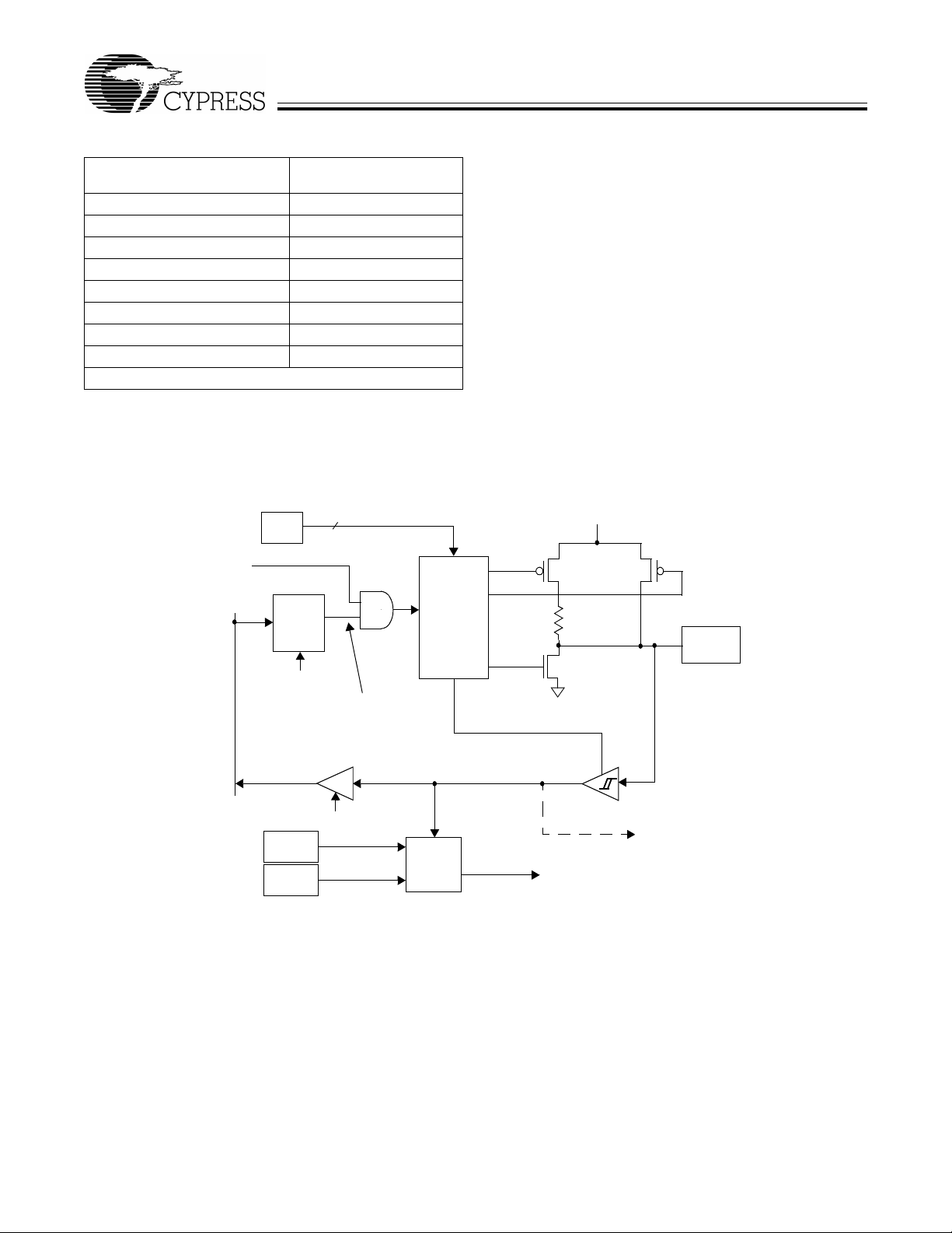
9.0 Clocking
The chip can be c locked f rom eithe r the i nternal on -chip cl ock,
or from an oscilla tor based on an external reso nator/crystal , as
shown in Figure 9-1. No additional capaci t an ce is included on
chip at the XTALIN/OUT pins. Operation is controlled by the
Clock Configuration Register, Figure 9-2.
Int Clk Output Disable
Internal Osc
Ext Clk Enable
CY7C63722
CY7C63723
CY7C63743
XTALOUT
Clk2x (12 MHz)
(to Microcontroller)
Clock
Doubler
XTALIN
Clk1x (6 MHz)
(to USB SIE)
Port 2.1
Figure 9-1. Clock Oscillator On-chip Circuit
Bit # 76543210
Bit Name Ext. Clock
Resume
Delay
Wake-up Timer Adjust Bit [2:0] Low-voltage
Reset
Disable
Precision
USB
Clocking
Enable
Internal
Clock
Output
Disable
External
Oscillator
Enable
Read/Write R/W R/W R/W R/W R/W R/W R/W R/W
Reset 00000000
Figure 9-2. Clock Configuration Register (Address 0xF8)
Bit 7: Ext. Clock Resume Delay
External Clock Resume Delay bit selects the delay time
when switching to the external oscillator from the internal
oscillator mode, or when waking from suspend mode with
the external oscillator enabled.
1 = 4 ms delay.
0 = 128 µs delay.
The delay gives the oscillator time to start up. The shorter
time is adequate for operation with ceramic resonators,
while the longer time i s preferre d for sta rt-up with a crys ta l.
(These times do not include an initial oscillator start-up
time which depends on the resonating element. This time
Bit [6:4]: Wake-up Timer Adjust Bit [2:0]
The Wake-up Timer Adjust Bits are used to adjust the
Wake-up timer period.
If the Wake-up interrupt is enabled in the Global Interrupt
Enable Register, the microc ontro ll er wi ll generate wake-up
interrupts periodically. The frequency of these periodical
wake-up interrupts is adjuste d by setting the Wake-up T imer Adjust Bit [2:0], as described in Section 11.2. One common use of the wake-up inte rrupts is to generate peri odical
wake-up events during suspend mode to check for changes, such as looking for movement in a mouse, while maintaining a low average power.
is typically 50–100 µs for ceramic resonators and 1–10 ms
for crystals). Note that th is bit only select s the delay time for
the external clock mode. When waking from suspend mode
with the internal oscillator (Bit 0 is LOW), the delay time is
only 8 µs in addition to a delay of app roximately 1 µs for the
oscillator to start.
Bit 3: Low-voltage Reset Disable
When V
ue of V
the microcontroller enters a partial suspend state for a period of t
Program execution begins from address 0x0000 after this
t
START
drops below V
CC
) and the Low-voltage Reset circuit is enabled,
LVR
(see Section 26 .0 for the value of t
START
delay period. This prov ide s ti me fo r VCC to stabilize
(see Section 25. 0 f or t he va l-
LVR
START
).
Document #: 38-08022 Rev. *B Page 10 of 49
Page 11

FOR
FOR
CY7C63722
CY7C63723
CY7C63743
before th e part ex ecut es code . Se e S ectio n 1 0.1 fo r mor e
details.
1 = Disables the LVR circuit.
0 = Enables t he LVR circuit.
Bit 2: Precision USB Clocking Enable
The Precision USB Clocking Enable only affects operation
in internal oscillator m od e. In tha t mode , this bit mus t be
set to 1 to cause the internal clock to au tomatically precisely tune to USB timing requirement s (6 M Hz ± 1.5% ).
The frequen cy may have a l ooser initia l tol eranc e at po wer-up, but all USB trans missions from t he ch ip will meet th e
USB specification.
1 = Enabled. The internal clock accuracy is 6 MHz ±1.5%
after USB traffic is received.
0 = Disabled. The internal clock accuracy is 6 MHz ±5%.
Bit 1: Internal Clock Output Disable
The Internal Clock Output Dis able is used to keep the int ernal clock from driving out to the XTALOUT pin. This bit has
no effect in the external oscillator mode.
1 = Disable int ernal clock out put. XTALOUT pin will drive
HIGH.
0 = Enable the internal clock output. The internal clock is
driven out to the XTALOUT pin.
Bit 0: External Oscillator Enable
At power-up, the chip operates from the internal clock by
default. Setting the Exte rnal Oscillato r Enable bit HIGH disables the internal clock, and halt s the part while the external
resonator/crystal oscillator is started. Clearing this bit has
no immediate effect, although the state of this bit is used
when waking out of su spend mod e to select be tween internal and external clock. In internal clock mode, XTALIN pin
will be confi gured as an i nput with a we ak pull-dow n and
can be used as a GPIO input (P2.1).
1 = Enable the external oscillator. The clock is switched to
external clock mode, as described in Section 9.1.
0 = Enable the internal oscillator.
9.1 Internal/External Oscillator Opera ti on
The internal oscillat or pro vi des an ope rati ng c lo ck , fac tory set
to a nominal frequency of 6 MHz. This clock requires no
external componen ts. At power-up, th e chip operates from the
internal clock. In this mode, the internal clock is buffered and
driven to the XTALOUT pin by default, and the state of the
XT ALIN pin ca n be read at Port 2.1 . While the inte rnal cl ock i s
enabled, its output can be disabled at the XTALOUT pin by
setting the Internal Clock Output Disable bit of the Clock
Configurat ion Register.
Setting the External Oscillator Enable bit of the Clock Configuration Register HIGH disables the internal clock, and halts
the part while the external resonator/crystal oscillator is
started. The steps involved in switching from Internal to
External Clock mode are as follows:
1. At reset, chip begins operation using the internal clock.
2. Firmware sets Bit 0 of the Clock Configuration R egister. For
example,
mov A, 1h ; Set Bit 0 HIGH (External Oscil-
lator Enable bit). Bit 7 cleared
gives faster start-up
iowr F8h ; Write to Clock Configuration
Register
3. Internal clocking is halted, the internal oscillator is disabled,
and the external clock oscillator is enabled.
4. After the external clock becomes stable, chip clocks are
re-enabled using the external clock signal. (Note that the
time for the externa l clock to become st able depends on the
external resonating device; see next sect ion.)
5. After an additional delay the CPU is released to run. This
delay depends on the state of the Ext. Clock Res ume Delay
bit of the Clock Configu r ati on Register. The time is 128 µs
if the bit is 0, or 4 ms if the bit is 1.
6. Once the chip has been set to external osc illator , it can only
return to internal clock when waking from suspend mode.
Clearing bit 0 of the Clock Configuration Register will not
re-enable internal clock mode until suspend mode is
entered. See Section 11.0 for more details on suspend
mode operation.
If the Internal Clock is enabled, the XTALIN pin can serve as
a general purpose input, and its state can be read at Port 2,
Bit 1 (P2.1). Refer to Figure 12-8 for the Port 2 Data Register.
In this mode, there is a weak pull-down at the XTALIN pin. This
input cannot provide an interrupt source to the CPU.
9.2 External Oscillator
The user can connect a low-cost ceramic resonator or an
external oscillator to the XTALIN/XTALOUT pins to provide a
precise reference frequency for the chip clock, as shown in
Figure 9-1. The external components required are a ceramic
resonator or crystal and any associated capacitors. To run
from the external resonator, the External Oscillator Enable bit
of the Clock Configuration Register must be set to 1, as
explained in the previous section.
Start-up times for the external oscillator depend on the
resonating device. Ceramic resonator based oscillators
typically start in less than 100 µs, while crystal based oscillators take longer, typically 1 to 10 ms. Board capacitance
should be minimized on the XTALIN and XTALOUT pins by
keeping the traces as short as possible.
An external 6-MHz clock can be applied to the XTALIN pin if
the XTALOUT pin is left open.
10.0 Reset
The USB Controller supports three types of resets. The effects
of the reset are listed below. The reset types are:
1. Low-voltage Reset (L VR)
2. Brown Out Reset (BOR)
3. Watchdog Reset (WDR)
The occurrence of a re se t is rec ord ed in the Proc es so r Status
and Control Register (Figure 20-1). Bits 4 (Low-voltage or
Brown-out Reset bit) and 6 (Watchdog Reset bit) are used to
record the occurrence of LVR/BOR and WDR respectively.
The firmware can i nterrogate these bit s to determine the cause
of a reset.
Document #: 38-08022 Rev. *B P age 11 of 49
Page 12
FOR
FOR
CY7C63722
CY7C63723
CY7C63743
The microcontroller begins execution from ROM address
0x0000 after a LVR, BOR, or WDR reset. Although this looks
like interrupt vector 0, there is an important difference. Reset
processing does NOT push th e program count er, carry flag,
and zero flag onto program stack. Attem pting to execute eith er
a RET or RETI in the reset handler will cause unpredictable
execution results.
The following events take place on reset. More details on the
various resets are given in the following sections.
1. All registers are reset to their default states (a ll bits cleared,
except in Processor Status and Control Register).
2. GPIO and USB pins are set to high-impedance state.
3. The VREG pi n is set to high-impedance state.
4. Interrupts are disabled.
5. USB operation is disabled and must be enable d by firmware
if desired, as explained in Section 14.1.
6. For a BOR or LVR, the external oscillator is disabled and
Internal Clock mode is activ ated , follo w ed by a time -out
period t
the clock mode, and there is no delay fo r V
on a WDR. Note that th e Ex tern al Os ci ll ator Enable (Bit 0,
for VCC to stabilize. A WDR does not ch ange
START
CC
stabilization
Figure 9-2) will be cleared by a WDR, but it does not take
effect until suspend mode is entered.
7. The Program Stack Pointer (PSP) and Data Stack Pointer
(DSP) reset to address 0x00. Firmware should move the
DSP for USB applications, as explained in Section 6.5.
8. Program execution beg ins at address 0x0000 after the
appropriate time-out period.
10.1 Low-voltage Reset (LVR)
When V
started and the Low-voltage Reset is initially enabled by
default. At the point where V
Section 25.0 for the value of V
counting for a period of t
of t
START
a partial sus pend state to wait fo r V
begins executing code from address 0x0000.
As long as the LVR circuit is enabled, this reset sequence
repeats wheneve r the V
LVR can be disabled by firmware by setting the Low-voltage
is first applied to the chip, the internal oscillator is
CC
has risen above V
). During this t
CC
), an internal counter starts
LVR
(see Section 26.0 for the value
START
time, the microcontroller enters
START
pin voltage drops below V
CC
to stabilize before it
CC
LVR
LVR
(see
. The
Reset Disable bit in the Clock Configuration Register
(Figure 9-2). In addition, the LVR is automatically disabled in
suspend mode to save power. If the LVR was enabled before
entering suspend mode, it becomes active again once the
suspend mode ends.
When L VR is di sabled duri ng normal operati on (i.e., by wri ting
‘0’ to the Low-voltage Reset Disable bit in the Clock Configuration Register), the chip may enter an unknown state if V
drops below V
times during normal operation. If LVR is disabled (i.e., by
. Therefore, LVR should be enabled at all
LVR
CC
firmware or during suspend mode), a secondary low-voltage
monitor, BOR, becomes active, as described in the next
section. The LVR/BOR Reset bit of the Processor Status and
Control Reg ister (Figure 20-1), is set to ‘1’ if either a LVR or
BOR has occurred.
10.2 Brown Out Reset (BOR)
The Brown Out Reset (BOR) circuit is always active and
behaves like the POR. BOR is asserted whenever the V
voltage to the d evice i s below an internally defined t rip volt age
CC
of approximately 2.5V. The BOR re-enables L VR. That is, onc e
drops and trips BOR, the part remains in reset until V
V
CC
rises above V
normal operation resumes, and the microcontroller starts
executing code from address 0x00 after the t
. At that point, the t
LVR
delay occurs befo re
START
START
delay.
CC
In suspend mode, only the BOR detection is active, giving a
reset if V
is suspended and code is not executing, this lower reset
drops below approxi mately 2.5 V. Since the device
CC
voltage is safe for retaining the state of all registers and
memory. Note that in suspend mode, LVR is disabled as
discussed in Section 10.1.
10.3 Watchdog Reset (WDR)
The Watchdog Timer Reset (WDR) occurs when the internal
Watchdog timer rolls over. Writing any value to the write-only
Watchdog Reset R egis ter at add ress 0x 26 will clear t he time r.
The timer will roll over and WDR will occur if it is not cleared
within t
(Watchdog Reset bit) of the Processor Status and Control
Register is set to reco rd th is ev ent (see Section 20.0 for mo re
details). A Watchdog Timer Reset typically lasts for 2–4 ms,
after which the microcontroller begins execution at ROM
address 0x0000.
(see Figure 10-1) of the last clear. Bit 6
WATCH
t
WATCH = 10.1 to
14.6 ms
WDR
(at F
OSC
= 6 MHz)
2–4 ms
At least 10.1 ms
since last write to WDR
WDR goes HIGH
for 2–4 ms
Execution begins at
ROM Address 0x0000
Figure 10-1. Watchdog Reset (WDR, Address 0x26)
Document #: 38-08022 Rev. *B Page 12 of 49
Page 13

FOR
FOR
CY7C63722
CY7C63723
CY7C63743
11. 0 Suspend Mode
The CY7C637xx parts support a versatile low-po wer s us pen d
mode. In suspend mode, only an enabled interrupt or a LOW
state on the D–/SDA TA pin will wake the part. Two options are
available. For lowest power, all internal circuits can be
disabled, so only an external event will resume operation.
Alternatively, a low- powe r internal wake-up time r ca n be used
to trigger the wake-up interrupt. This timer is described in
Section 11.2, and can be used to periodically poll the system
to check for changes, such as looking for movement in a
mouse, while maintaining a low average power.
The CY7C637xx is pla ced into a low-power st ate by setting the
Suspend bit of the Processor Status and Control Register
(Figure 20-1). All logic blocks in the device are turned off
except the GPIO interrupt logic, the D–/SDATA pin input
receiver, and (optio nally) the w ake-up tim er. The clock oscillators, a s well as th e free-runnin g and Watchdog ti mers are
shut down. Only the occurr ence of an enabled GPIO int errupt,
wake-up interrupt, SPI slave interrupt, or a LOW state on the
D–/SDATA pin will wake the part from suspend (D– LOW
indicates non-idle USB activity). Once one of these resuming
conditions occurs, clocks will be restarted and the device
returns to full operation after the oscillator is stable and the
selected delay period expires. This d elay pe riod is determine d
by selection of internal vs. external clock, and by the state of
the Ext. Clock Resume Delay as explained in Section 9.0.
In suspend mode, any en abled and pending interrup t will wake
the part up. The state of the Interrupt Enable Sense bit (Bit 2,
Figure 20-1) does not have any effect. As a result, any interrupts not inte nded for waking from suspend should be disabled
through the Global Int errupt Enable Register a nd the USB End
Point Interrupt Enable Register (Section 21.0).
If a resuming conditi on e xi st s whe n th e s us pen d bi t is se t, th e
part will still go into suspend and then awake after the appropriate delay time. The Run bit in the Processor Status and
Control Register must be set for the part to resume out of
suspend.
Once the clock is stable and the delay time has expired, the
microcontroller will execute the instruction following the I/O
write that placed the device into suspend mode before
servicing any interrupt requests.
To achieve the lowes t pos si ble curre nt duri ng su spend mode,
all I/O should be held at either V
GPIO bit interrupts (Figure 21-4 and Figure 21-5) should be
disabled for any pins that are not being used for a wake-up
interrupt. This s hould be d one e ven i f the main GPIO Interru pt
Enable (Figure 21-1) is off.
Typical code for entering suspend is shown below:
... ; All GPIO set to low-power st ate (no floating
pins, and bit interrupts disabled unless
using for wake-up)
... ; Enable GPIO and/or wake-up timer
interrupts if desired for wake-up
... ; Select clock mode for wake-up (see
Section 11.1)
mov a, 09h ; Set suspend and run bits
iowr FFh ; Write to Status and Control Register –
Enter suspend, wait for GPIO/wake-up
interru pt or USB activity
nop ; This executes before any ISR
... ; Remaining code for exiting suspend
routine
or ground. In addition, the
CC
11.1 Clocking Mode on Wake-up from Suspend
When exiting suspend on a wake-up event, the device can be
configured to run in either Internal or External Clock mode.
The mode is selected by the state of the External Oscillator
Enable bit in the Clock Configuration Register (Figure 9-2).
Using the I nt e rna l Cl oc k s a ve s t he ex t er nal o sc i ll at o r s tart - up
time and keeps that os cill ator of f for a ddi tional power sa vi ngs.
The external oscillator mode can be activated when desired,
similar to operation at power-up.
The sequence of events for these modes is as follows:
Wake in Internal Clock Mode:
1. Before entering suspend, clear bit 0 of the Clock Configuration Register. This selects Internal clock mode after suspend.
2. Enter suspend mode by setting the suspend bit of the
Processor Status and Control Register.
3. After a wake-up event, the i nternal clock st arts imm ediately
(within 2 µs).
4. A time-out period of 8 µs pas ses, and then firmware
execution begins.
5. At some later point, to activate Exte rnal Clock mode, s et bit
0 of the Clock Configur ation Register . This halts the internal
clocks while the external clock becomes stable. After an
additional time-out (128 µs or 4 ms, see Section 9.0),
firmware execution resumes.
Wake in External Clock Mode:
1. Before entering suspend, the external clock mu st be selected by setting bit 0 o f the Clock Configuration Regi ster. Make
sure this bit is sti ll set when suspend mode is entered. T his
selects External clock mode after suspend.
2. Enter suspend mode by setting the suspend bit of the
Processor Status and Control Register.
3. After a wake-up event, the external oscill ator is started. The
clock is monitored for stability (this takes approximately
50–100 µs with a ceramic resonator).
4. After an additional time-out period (128 µs or 4 ms, see
Section 9.0), firmware execution resumes.
11.2 Wake-up Timer
The wake-up timer runs whenever the wake-up interrupt is
enabled, and is turned off whenever that interrupt is disabled.
Operation is independent of whether the device is in suspend
mode or if the global inter rupt bit is enabled. On ly the Wak e-up
Timer Interrupt Enable bit (Figure 21-1) controls the wake-up
timer.
Once this timer is activated, it will give interrupts after its
time-out period (see below). These in terrupts continue p eriodically until the interrupt is disabled. Whenever the interrupt is
disabled, the wake-up timer is reset, so that a subsequent
enable always results in a full wake-up time.
The wake-up timer can be adjusted by the user through the
Wake-up Timer Adjust bits in the Clock Configuration Register
(Figure 9-2). These bits clear on reset. In addition to allowing
the user to select a range for the wake-up time, a firmware
algorithm can be used to tune out initial pr ocess and o perating
condition variatio ns in this w ake-up time. Thi s can be do ne by
timing the wake-up interrupt time with the accurate 1.024-ms
timer interrupt, and a djusting the T imer Adjus t bits accordin gly
to approximate the desired wake-up time.
Document #: 38-08022 Rev. *B Page 13 of 49
Page 14
FOR
FOR
Table 11-1. Wake-up Timer Adjust Settings
Adjust Bits [2:0]
(Bits [6:4] in Figure 9-2) Wake-up Time
000 (reset state) 1 * t
001 2 * t
010 4 * t
01 1 8 * t
100 16 * t
101 32 * t
110 64 * t
111 128 * t
See Section 26.0 for the value of t
WAKE
WAKE
WAKE
WAKE
WAKE
WAKE
WAKE
WAKE
WAKE
12.0 General Purpose I/O Ports
Ports 0 and 1 provide up to 16 versati le GPIO pins that can be
read or written (the number of pins dep ends on package typ e).
Figure 12-1 shows a diagram of a GPIO port pin.
CY7C63722
CY7C63723
CY7C63743
2
(Data Reg must be 1
for SPI outputs)
Port Read
Interrupt
Logic
SPI Bypass (P0.5–P0.7 only)
(=1 if SPI inactive, or for non-SPI pins)
Internal
Data Bus
GPIO
Mode
Data
Out
Register
Port Write
Interrupt
Polarity
Interrupt
Enable
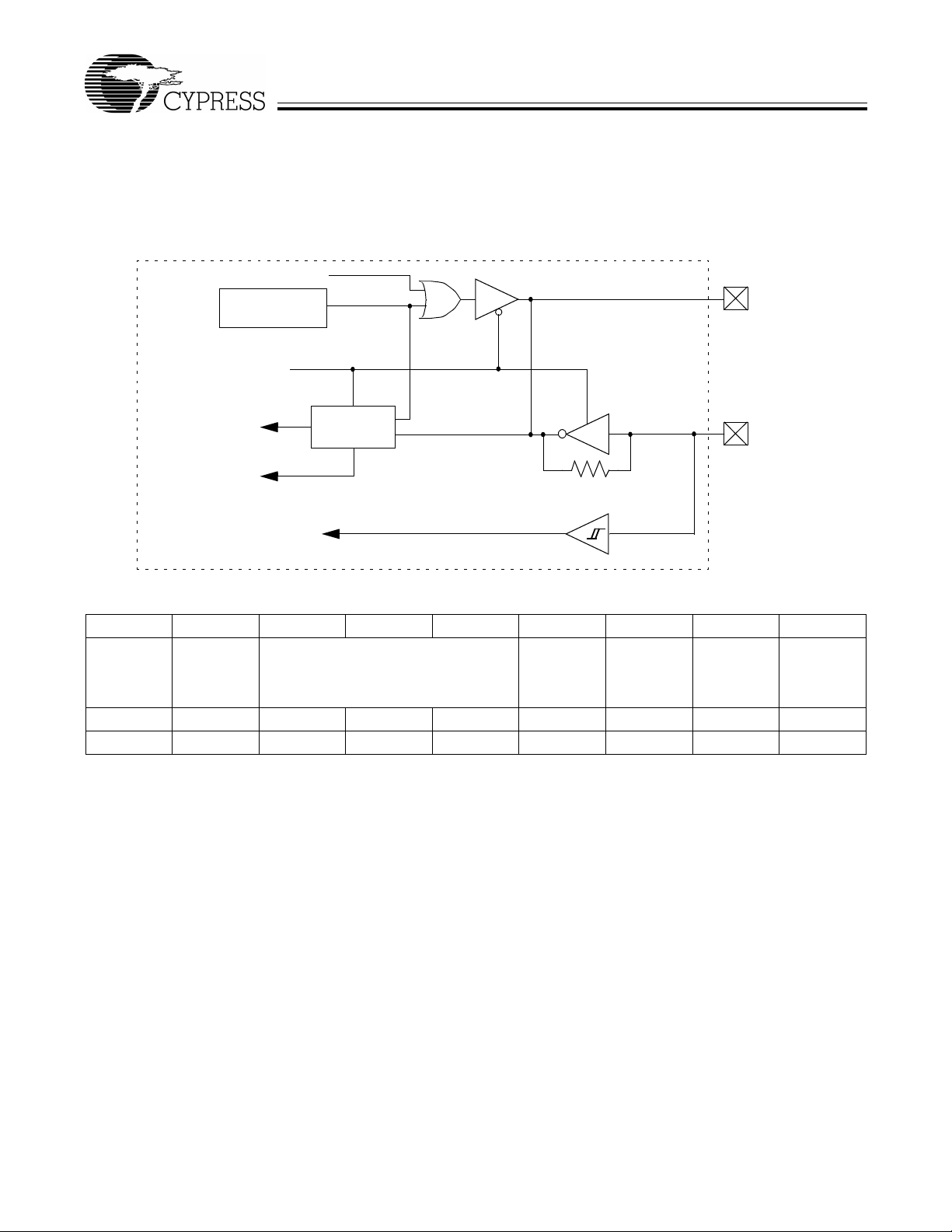
Figure 12-1. Block Diagram of GPIO Port (one pin shown)
Port 0 is an 8-bit port; Port 1 con t ai ns eith er 2 b it s , P1. 1–P1.0
in the CY7C63723, or all 8 bits , P1.7–P1.0 i n the C Y7C6 3743
parts. Each bit c an a ls o be sel ec ted as an i nterr upt s ou rce for
the microcontroller, as explained in Section 21.0.
The data for each GPIO pin is accessible through the Port
Data registe r. Writes to the P ort Data r egiste r store outgoing
data state for the port pins, while reads from the Port Data
register return the actual logic value on the port pins, not the
Port Data register contents.
V
CC
Q1
Control
14 kΩ
Q3
GPIO
Pin
Q2
Threshold Select
To Capture Timers (P0.0, P0.1)
and SPI (P0.4–P0.7))
To Interrupt
Controller
Each GPIO pin is configured inde pendently. The driving state
of each GPIO pin is determin ed by the value written to th e pin’s
Data Registe r and by two assoc iat ed pin’s Mode0 and M ode1
bits.
The Port 0 Data Register is sh own in Figure 12-2, and the Port
1 Data Register is shown in Figure12-3. The Mode0 and
Mode1 bits for the two GPIO ports are given in Figure 12-4
through Figure 12-7.
Document #: 38-08022 Rev. *B Page 14 of 49
Page 15

FOR
FOR
CY7C63722
CY7C63723
CY7C63743
Bit # 76543210
Bit Name P0
Read/Write R/WR/WR/WR/WR/WR/WR/WR/W
Reset 00000000
Figure 12-2. Port 0 Data (Address 0x00)
Bit [7:0]: P0[7:0]
1 = Port Pin is logic HIGH
0 = Port Pin is logic LOW
Bit # 76543210
Bit Name P1
Notes Pins 7:2 only in CY7C63743 Pins 1:0 in
all parts
Read/Write R/W R/W R/W R/W R/W R/W R/W R/W
Reset 00000000
Figure 12-3. Port 1 Data (Address 0x01)
Bit [7:0]: P1[7:0]
1 = Port Pin is logic HIGH
0 = Port Pin is logic LOW
Bit # 76543210
Bit Name P0[7:0] Mode0
Read/Write WWWWWWWW
Reset 00000000
Figure 12-4. GPIO Port 0 Mode0 Register (Address 0x0A)
Bit [7:0]: P0[7:0] Mode 0
1 = Port 0 Mode 0 is logic HIGH
0 = Port 0 Mode 0 is logic LOW
Bit # 76543210
Bit Name P0[7:0] Mode1
Read/Write WWWWWWWW
Reset 00000000
Figure 12-5. GPIO Port 0 Mode1 Register (Address 0x0B)
Bit [7:0]: P0[7:0] Mode 1
1 = Port Pin Mo de 1 is logic HIGH
0 = Port Pin Mode 1 is logic LOW
Bit # 76543210
Bit Name P1[7:0] Mode0
Read/Write WWWWWWWW
Reset 00000000
Figure 12-6. GPIO Port 1 Mode0 Register (Address 0x0C)
Bit [7:0]: P1[7:0] Mode 0
1 = Port Pin Mode 0 is logic HIGH
0 = Port Pin Mode 0 is logic LOW
Bit # 76543210
Bit Name P1[7:0] Mode1
Read/Write WWWWWWWW
Reset 00000000
Figure 12-7. GPIO Port 1 Mode1 Register (Address 0x0D)
Bit [7:0]: P1[7:0] Mode 1
1 = Port Pin Mode 1 is logic HIGH
0 = Port Pin Mode 1 is logic LOW
Each pin can be independe ntly configure d as high-impedanc e
inputs, inputs with internal pull-ups, open drain outputs, or
traditional CMOS outputs with selectable drive strengths.
The driving state of ea ch GPIO pin is determi ned by the valu e
written to the pin ’s Da ta Regis ter and by its associat ed Mode0
and Mode1 bits. Table 12-1 lists the configuration states
based on these bits. The GPIO ports default on reset to all
Data and Mode Registers cleared, so the pins are all in a
high-impedance state. The available GPIO output drive
strength are:
• Hi-Z Mode (Mode1 = 0 and Mode0 = 0)
Q1, Q2, and Q3 (Figure 12-1) are OFF . The GPIO pin is not
driven internally . Perfo rming a read from the Port Data Register return the actual logic value on the port pins.
• Low Sink Mode (Mode1 = 1, Mode0 = 0, and the pin ’s Data
Register = 0)
Q1 and Q3 are OFF. Q2 is ON. The GPIO pin is capable of
sinking 2 mA of current.
• Medium Sink Mode (Mode1 = 0, Mode0 = 1, and the pin’s
Data Register = 0)
Q1 and Q3 are OFF. Q2 is ON. The GPIO pin is capable of
sinking 8 mA of current.
• High Sink Mode (Mode1 = 1, Mode 0 = 1, and the pin’s Dat a
Register = 0)
Q1 and Q3 are OFF. Q2 is ON. The GPIO pin is capable of
sinking 50 mA of current.
• High Drive Mode (Mode1 = 0 or 1, Mode0 = 1, and the pin’s
Data Register = 1)
Q1 and Q2 are OFF. Q3 is ON. The GPIO pin is capable of
sourcing 2 mA of current.
• Resistive Mode (Mode 1 = 1, Mode0 = 0, and the pin ’s Data
Register = 1)
Q2 and Q3 are OFF. Q1 is ON. The GPIO pin is pulled up
with an internal 14-kΩ resistor.
Note that open drain mode can be achieved by fixing the Data
and Mode1 Registe rs LOW , an d switching t he Mode0 regi ster .
Input thresholds are CMOS, or TTL as sh own in the t able (See
Section 25.0 for the input threshold voltage in TTL or CMOS
modes). Both input modes include hysteresis to minimize
noise sensitivity. In suspend mode, if a pin is used for a
wake-up interrupt using an external R-C circuit, CMOS mode
is preferred for lowest power.
Document #: 38-08022 Rev. *B Page 15 of 49
Page 16

FOR
FOR
CY7C63722
CY7C63723
CY7C63743
Table 12-1. Ports 0 and 1 Output Control Truth Table
Data
Register
0
1Hi-ZTTL
0
1High DriveCMOS
0
1ResistiveCMOS
0
1High DriveCMOS
Mode1 Mode0 Output Drive
00
01
10
11
Strength
Hi-Z CMOS
Medium
(8 mA) Sink
Low (2 mA)
Sink
High (50 mA)
Sink
Input
Threshold
CMOS
CMOS
CMOS
12.1 Auxiliary Input Port
Port 2 serves as an auxiliary input port as shown in
Figure 12-8. The Port 2 inputs all have TTL input thresholds .
Bit # 7 6 5 4 3 2 1 0
Bit
Reserved D+
Name
Read/
Write
Reset 00 0 0 00 0 0
Bit [7:6]: Reserved
Bit [5:4]: D+ (SCLK) and D– (SDATA) States
Bit [3:2]: Reserved
Bit 1: P2.1 (Internal Clock Mode Only)
Bit 0: P2.0/VREG Pin State
-- R R -- R R
Figure 12-8. Port 2 Data Register (Address 0x02)
The state of the D+ and D– pi ns can be read a t Port 2 Dat a
Register . P erformi ng a read fro m the po rt pins returns their
logic values.
1 = Port Pin is logic HIGH
0 = Port Pin is logic LOW
In the Internal Clock mode, the XTALIN pin can serve as a
general purpose input, and its state can be read at Port 2,
Bit 1 (P2.1). See Section 9.1 for more details.
1 = Port Pin is logic HIGH
0 = Port Pin is logic LOW
In PS/2 mode, the VREG
its state can be r ead at port P2.0 . Section 15.0 f or more
details.
1 = Port Pin is logic HIGH
0 = Port Pin is logic LOW
(SCLK)
State
D–
(SDATA)
State
Reserved P2.1
pin can be used as an input and
(Internal
Clock
Mode
Only)
P2.0
VREG
Pin
State
13.0 USB Serial Interface Engine (SIE)
The SIE allows the microcontroller to communicate with the
USB host. The SIE simplifies the interface be tween the mic rocontroller and USB by incor porating hardware that ha ndles the
following USB bus activity independently of the microcontroller:
• Translate the encoded recei ved data and format the data to
be transmitted on the bus.
• CRC checking and generation. Flag the microcontroller if
errors exist during transmission.
• Address checking. Ignore the transactions not addressed
to the device.
• Send appropriate ACK/NAK/STALL handshakes.
• Token type identification (SETUP, IN, or OUT). Set the ap-
propriate token bit once a valid token is received.
• Place valid received data in the appropriate endpoint FIFOs.
• Send and update the data toggle bit (Data1/0).
• Bit stuffing/unstuffing.
Firmware is required to handle the rest of the USB interface
with the following tasks:
• Coordinate enumera tion by decoding USB d evice requests.
• Fill and empty the FIFOs.
• Suspend/Resume coordination.
• Verify and select Data toggle values.
13.1 USB Enumeration
A typical USB enumeration sequence is shown below. In this
description, ‘Firmware’ refers to embedded firmware in the
CY7C637xx controller.
1. The host computer sends a SETUP packet followed by a
DATA packet to USB address 0 requesting the Device descriptor.
2. Firmware decodes the request and retrieves its Device
descriptor from the program memory tables.
3. The host computer performs a control read se qu enc e an d
Firmware responds by sendin g the Devic e descripto r over
the USB bus, via the on-chip FIFO.
4. After receiving the descriptor, the host sends a SETUP
packet followed by a DATA packet to address 0 assigning
a new USB address to the device.
5. Firmware stores the new address in its USB Device
Address Register after the no-data control sequence
completes.
6. The host sends a request for the Device descriptor using
the new USB address.
7. Firmware decodes the request and retrieves the Device
descriptor from program memory tables.
8. The host performs a control read sequence a nd Fi rmwa re
responds by sending its Device descriptor over the USB
bus.
9. The host generates control reads fro m the device to request
the Configuration and Report descriptors.
10.Once the device receives a Set Configuration request, its
functions may now be used.
11.Firmware should take appropriate action for Endpoint 1
and/or 2 transactions, which may occur from this point.
Document #: 38-08022 Rev. *B Page 16 of 49
Page 17

FOR
FOR
CY7C63722
CY7C63723
CY7C63743
13.2 USB Port Status and Control
USB status and control is regulated by the USB Status and
Control Register as shown in Figure 13-1.
Bit # 76 5 4 3 2:0
Bit
PS/2
Name
Pull-up
Enable
Enable
VREG
Read/
R/W R/W R/W - R/W R/W
Write
Reset 00 0 0 0000
Figure 13-1. USB Status and Control Register (Address
Bit 7: PS/2 Pull-up Enable
This bit is used to enab le the intern al PS/2 pull-u p resisto rs
on the SDATA and SCLK pins. Normally the output high
level on these pins is V
clamped to approximately 1 Volt above V
Enable bit is set, or if the Device Address is enabled (bit 7
of the USB Device Address R egister, Figure 14-1).
1 = Enable PS/2 Pull-up resistors. The SDATA and SCLK
pins are pulled up internally to V
approximately 5 kΩ (see Section 25.0 for the value of
).
R
PS2
0 = Disable PS/2 Pull-up resistors.
Bit 6: V
REG
Enable
A 3.3V voltage regulator is integrated on chip to provide a
voltage source for a 1.5-kΩ pull-up resistor connected to
the D– pin as required by the USB Specification. Note that
the VREG output has an internal series resistance of approximately 200Ω, the external pull-up resistor required is
approximately 1.3-kΩ (see Figure 16-1).
1 = Enable the 3.3V output voltage on the VREG pin.
0 = Disable. The VREG pin can be configured as an input.
Bit 5: USB-PS/2 Interrupt Select
This bit allows the us er to selec t whether an U SB bus reset
interrupt or a PS/2 activi ty interru pt wi ll be gen erated whe n
the interrupt conditions are detected.
USB
Reset-
PS/2
Reserved USB
Bus
Activity
Activity
Interrupt
Mode
0x1F)
, but note that the output will be
CC
REG
with two resi stors of
CC
D+/D–
Forcing
Bit
if the VREG
1 = PS/2 interrupt mode. A PS/2 a ctivity i nterrupt wi ll occur
if the SDATA pin is continuously LOW for 128 to 256 µs.
0 = USB interrupt mode (default st ate). In this mode, a USB
bus reset interrupt w il l o ccur i f the single ended ze ro (SE 0,
D– and D+ are LOW) exists for 128 to 256 µs.
See Section 21.3 for more details.
Bit 4: Reserved. Must be written as a ‘0’.
Bit 3: USB Bus Activity
The Bus Activity bit is a “sticky” bit that detects any non-idle
USB event has occurred on the USB bus. Once set to HIGH
by the SIE to indicate the bus activity, this bit retains its
logical HIGH value until firmware clears it. Writing a ‘0’ to
this bit clears it; writing a ‘1’ preserves its value. The user
firmware sh ou ld ch ec k an d cle a r thi s bit pe r i od ic all y t o de tect any loss of bus activity. Firmware can clear the Bus
Activity bit, but only the SIE can set it. The 1.024-ms timer
interrupt service routi ne is normally used to check an d clear
the Bus Activity bit.
1 = There has been bus activity since the last time this bit
was cleared. This bit is set by the SIE.
0 = No bus activit y since l ast time this bit wa s cleare d (by
firmware).
Bit [2:0]: D+/D– Forcing Bit [2:0]
Forcing bits al lo w fir m war e t o dir e ctl y d r iv e t he D + and D –
pins, as shown in Table 13-1. Outputs are driven with controlled edge rates in these modes for low EMI. For forcing
the D+ and D– pins in USB mode, D+ /D– Forcing Bit 2
should be 0. Setting D+/D– Forcing Bit 2 to ‘1’ puts both
pins in an open-dra in mode, pref erred for applic ations such
as PS/2 or LED driving.
Table 13-1. Control Modes to Force D+/D– Outputs
D+/D– Forcing
Control Action Application
Bit [2:0]
000 Not forcing (SIE controls driver) Any Mode
001 Force K (D+ HIGH, D– LOW) USB Mode
010 Force J (D+ LOW, D– HIGH)
01 1 Force SE0 (D– LOW, D+ LOW)
100 Force D– LOW, D+ LOW PS/2 Mode
101 Force D– LOW, D+ HiZ
110 Force D– HiZ, D+ LOW
111 Force D– HiZ, D+ HiZ
[2]
Note:
2. For PS/2 operation, the D+/D– Forcing Bit [2:0] = 111b mode must be set initially (one time only) before using the other PS/2 force modes.
Document #: 38-08022 Rev. *B Page 17 of 49
Page 18

FOR
FOR
CY7C63722
CY7C63723
CY7C63743
14.0 USB Device
The CY7C637xx suppo rts one USB Device Address with three
endpoints: EP0, EP1, and EP2.
14.1 USB Address Register
The USB Device Address Register contains a 7-bit USB
address and one bit to enable USB communication. This
register is cleared during a reset, setting the USB device
address to zero and marking this address as disabled.
Figure 14-1 shows the format of the USB Address Register.
Bit # 7 6543210
Bit Name Device
Read/Write R/W R/W R/W R/W R/W R/W R/W R/W
Reset 0 0000000
Figure 14-1. USB Device Add ress Register (Address 0x10)
In either USB or PS/2 mode, this register is cleared by both
hardware resets and the U SB bus res et. Se e Sec tion 21.3 for
more information on the USB Bus Reset – PS/2 interrupt.
Bit 7: Device Address Enable
This bit must be enabled by firmware before the serial interface engine (SIE) will respond to USB traffic at the address specified in Bit [6:0].
1 = Enable USB device address.
0 = Disable USB device address.
Bit [6:0]: Device Address Bit [6:0]
These bits must be set by firmware during the USB enumeration process (i.e., SetAddress) to the non-zero address
assigned by the USB host.
Address
Enable
14.2 USB Control Endpoint
All USB devices are required to have an endpoint number 0
(EP0) that is used to initia lize and control th e USB device. EP0
provides access to the device configuration information and
allows generic USB status and control accesses. EP0 is
bidirectional as the device c an both rec eive and transmit data.
EP0 uses an 8-byte FIFO at SRAM locations 0xF8-0xFF, as
shown in Section 8.2.
The EP0 endpoint mode register uses the format shown in
Figure 14-2.
Bit # 765 4 3:0
Bit
SETUP
Name
Received
Read/
Write
Reset 000 00000
Figure 14-2. Endpoint 0 Mode Register (Address 0x12)
R/W R/W R/W R/W R/W
IN
Received
Device Address
OUT
Received
ACKed
Transaction
Mode Bit
The SIE provides a locking feature to prevent firmware from
overwriti ng b i ts i n t he U SB Endpo i nt 0 Mode R e gis te r. Writes
to the register have no effect from the poin t tha t Bit[ 6:0 ] of the
register are updated (by the SIE) until the firmware reads this
register. The CPU can unlock this register by reading it.
Because of these hardware-locking features, firmware should
perform an read after a write to the USB Endpoint 0 Mode
Register and USB Endpoint 0 Count Register (Figure 14-4) to
verify that the content s have changed as desired, and tha t the
SIE has not updated these values.
Bit [7:4] of this register are cleared by any non-locked write to
this register, regardless of the value written.
Bit 7: SETUP Received
1 = A valid SETUP packet has been received. This bit is
forced HIGH from the start of the data packet phase of the
SETUP tran saction until the sta rt of the ACK packet returned by the SIE. Th e CPU is p revente d from clearin g thi s
bit during this interval. While this bit is set to ‘1’, the CPU
cannot write to the EP0 FI FO . Th is prev en ts firmware from
overwriting an incoming SETUP transaction before firmware has a chance to read the SETUP data.
0 = No SETUP received. This bit is cleared by any
non-locked writes to the register.
Bit 6: IN Received
1 = A valid IN packe t has been rece ived. This bi t is updated
to ‘1’ after the la st received p acket in an IN transaction. This
bit is cleared by any non-locked writes to the register.
0 = No IN received. This bit is cleared by any non-locked
writes to the register.
Bit 5: OUT Received
1 = A valid OUT packet has been received. This bit is updated to ‘1’ after the last received packet in an OUT transaction. This bit is cleared by any non-locked writes to the
register.
0 = No OUT receiv ed. This bit is clea red by an y non- locked
writes to the register.
Bit 4: ACKed Transaction
The ACKed Trans action bit is s et whenever the SIE e ngages in a transaction to the register's endpoint that completes
with an ACK packet.
1 = The transaction completes with a n ACK.
0 = The transaction does not complete with an ACK.
Bit [3:0]: Mode Bit[3:0]
The endpoint modes determine how the SIE responds to
USB traffic that the host sends to the endpoint. For example, if the endpoint Mode Bit s [3:0] are set to 0001 whic h is
NAK IN/OUT mode as shown in Table 22-1, the SIE will
send NAK handshak es in response to any IN or OUT token
sent to this endp oint. In this NAK IN/OUT mod e, the SIE will
send an ACK handshake when the host sends a SETUP
token to this endpoint. The mode encoding is shown in
Table 22-1. Additional information on the mode b it s c an b e
found in Table 22-2 and Table 22-3. These modes give the
firmware total control on how to respond to different tokens
sent to the endpoints from the host.
Document #: 38-08022 Rev. *B Page 18 of 49
Page 19

FOR
FOR
CY7C63722
CY7C63723
CY7C63743
In addition, the Mode Bit s are automat ically ch anged by th e
SIE in response to many USB transactions. For exa mple, if
the Mode Bit [3:0] are set to 1011 which is ACK OUT-NAK
IN mode as show n in Table 22-1, the SIE will change the
endpoint Mode Bit [3:0] to NAK IN/OUT (0001) mode after
issuing an ACK handshake in response to an OUT token.
Firmware needs to update t he mode for th e SIE to respond
appropriately.
14.3 USB Non-control Endpoints
The CY7C637xx feature two non-control endpoints, endpoint
1 (EP1) and endpoint 2 (EP2). The EP1 and EP2 Mode
Registers do not have the locking mechanism of the EP0
Mode Register. The EP1 and EP2 Mode Registers use the
format shown in Figure 14-3. EP1 uses an 8-byte FIFO at
SRAM locations 0xF0–0xF7, EP2 uses an 8-byte FIFO at
SRAM locations 0xE8–0xEF as shown in Section 8.2.
Bit # 7 65 4 3210
Bit
STALL Reserved ACKed
Name
Read/
Write
Reset 0 00 0 0000
Figure 14-3. USB Endpoint EP1, EP2 Mode Registers (Ad-
Bit 7: STALL
Bit [6:5]: Reserved. Must be written to zero during register
writes.
R/W - - R/C R/W R/W R/W R/W
dresses 0x14 and 0x16)
1 = The SIE will stall an OUT packet if the Mode Bits are set
to ACK-OUT, and the SIE will stall an IN packet if the mode
bits are set to ACK-IN. See Section 22.0 for the available
modes.
0 = This bit must be set to LOW for all other modes.
Transaction
Mode Bit
14.4 USB Endpoint Counter Registers
There are three Endpoint Counter registers, with identical
formats for both control and non-control endpoints. These
registers contain by te count in formati on for USB transa ctions ,
as well as bits for data packet status. The format of these
registers is shown in Figure 14-4.
Bit # 7 6 5 43210
Bit Name Data
Toggle
Read/WriteR/W R/W - - R/WR/WR/WR/
Reset 0 0 0 0 0000
Figure 14-4. Endpoint 0,1,2 Counter Registers
(Addresses 0x11, 0x13 and 0x15)
Bit 7: Data Toggle
This bit selects the DATA packet's toggle state. For IN
transactions, firmware must set this bit to the select the
transmitted Data Toggle. For OUT or SETUP transactions,
the hardware sets this bit to the state of the received Data
Toggle bit.
1 = DA TA1
0 = DA TA0
Bit 6: Data Valid
This bit is used for OUT and SETUP toke ns only. This bit is
cleared to ‘0’ if CRC, bitstuff, or PID errors have occurred.
This bit does not update for some endpoint mode settings.
Refer to Table 22-3 for more details.
1 = Data is valid .
0 = Data is invalid. If enabled, the endpoint interrupt will
occur even if invalid data is received.
Bit [5:4]: Reserved
Data
Valid
Reserved Byte Count
W
Bit 4: ACKed Transaction
The ACKed transaction bit is set when ever the SIE enga ges in a transaction to the register's endpoint that completes
with an ACK packet.
1 = The transaction completes with an ACK.
0 = The transaction does not complete with an ACK.
Bit [3:0]: Mode Bit [3:0]
The EP1 and EP2 Mode Bits operate in the same manner
as the EP0 Mode Bits (see Section 14.2).
Document #: 38-08022 Rev. *B Page 19 of 49
Bit [3:0]: Byte Count Bit [3:0]
Byte Count Bits indicate the number of data bytes in a
transaction: For IN transactions, firmware loads the count
with the number of by te s to be transmitted to the h os t from
the endpoin t FIFO. Valid values are 0 to 8 inclusi ve. For
OUT or SETUP transac tions, the c ount is u pdated by hardware to the number of data bytes received, plus 2 for the
CRC bytes. Valid values are 2 to 10 inclusive.
For Endpoint 0 Count Register, whenever the count updates from a SETUP or OUT transaction, the count register
locks and cannot be written by the CPU. Reading the register unlocks it. This prevents firmware from overwriting a
status update on incoming SETUP or OUT transactions before firmware has a chance to read the data.
Page 20

FOR
FOR
CY7C63722
CY7C63723
CY7C63743
15.0 USB Regulator Output
The VREG pin provides a regulat ed out put for conn ec ting the
pull-up resistor req uired for USB operat ion. For USB, a 1 .5-kΩ
resistor is connected between the D– pin and the V
voltage, to indicate low-speed USB operation. Since the
VREG output has an internal series resistance of approximately 200Ω, the external pull-up resistor required is R
Section 25.0).
The regulator output is placed in a high-impedance state at
reset, and must be enabled by firmware by setting the VREG
Enable bit in the USB Status and Control Register
(Figure 13-1). This simplifies the design of a combination
PS/2-USB device, since the USB pul l-up resistor c an be left in
place during PS/2 operation without loading the PS/2 line. In
this mode, the V
can be read at port P2.0. Refer to Figure 12-8 for the Port 2
pin can be used as an input and its state
REG
data register. This input has a TTL threshold.
In suspend mode, the regulator is automatically disabled. If
VREG Enable bit is set (Figure 13-1), the VREG pin is pulled
up to V
proper V
with an internal 6.2-kΩ resistor. This holds the
CC
state in suspend mode
OH
Note that enabling the device for USB (by setting the Device
Address Enable bit, Figure 14-1) activates the internal
regulator, even if the VREG Enable bit is cleared to 0. This
insures proper USB sig naling in th e case wh ere the VREG pi n
is used as an input, and an external regulator is provided for
the USB pull-up resistor. This also limits the swing on the D–
and D+ pins to about 1V above the internal regulator voltage,
so the Device Address Enab le bit no rma ll y sh ould only be set
for USB operating modes.
The regulator output is only de signed to provide cu rrent for the
USB pull-up resistor. In addition, the output voltage at the
PU
REG
(see
VREG pin is effectively disconnected when the CY7C637xx
device transmits USB from the internal SIE. This means that
the VREG pin does not provide a stable voltage during
transmits, although this does not affect USB signaling.
16.0 PS/2 Operation
The CY7C637xx parts are optimized for combination USB or
PS/2 devices, through the following features:
1. USB D+ and D– lines can also be used for PS/2 SCLK and
SDATA pins, respectively. With USB disabled, these lines
can be placed in a hi gh-impeda nce st ate that w ill pull up to
. (Disable USB by clearing the Address Enable bit of
V
CC
the USB Device Address Register, Figure 14-1).
2. An interrupt is provided to indicate a long LOW state on the
SDA TA pin. This eliminat es the need to poll this pin to check
for PS/2 activity. Refer to Section 21.3 for more details.
3. Internal PS/2 pull-up resistors can be enabled on th e SCLK
and SDA T A lines, so no GPIO pins are req uired for this ta sk
(bit 7, USB Status and Control Register, Figure 13-1).
4. The controlled slew rate outputs from these pins apply to
both USB and PS/2 modes to minimize EMI.
5. The state of the SCLK and SDATA pins can be read, and
can be individually dri ven LOW in an open drain mode . The
pins are read at bits [5:4 ] of Port 2, and are drive n with the
Control Bits [2:0] of the USB Status and Control Register.
6. The V
so that a USB pull-up resi stor on the D–/SDATA pin will not
interfere with PS/2 ope ration (bit 6, USB S tatus and Co ntrol
Register).
The PS/2 on-chip support c ircuitry is illus trated in Figure 16-1.
pin can be placed into a high-impedance state,
REG
Port 2.0
VREG Enable
3.3V
200Ω
Regulator
V
CC
PS/2 Pull-up
Enable
5 kΩ
5 kΩ
USB - PS/2
Driver
Port 2.5
Port 2.4
On-chip Off-chip
Figure 16-1. Diagram of USB-PS/2 System Connections
VREG
1.3 kΩ
D+/SCLK
D–/SDATA
Document #: 38-08022 Rev. *B Page 20 of 49
Page 21

FOR
FOR
CY7C63722
CY7C63723
CY7C63743
17.0 Serial Peripheral Interface (SPI)
SPI is a four-wire, full-duplex serial communication interface
between a master devic e and one or m ore sl ave de vices . The
CY7C637xx S PI circuit supports byte se rial transfers in either
Master or Slave modes. The block diagram of the SPI circuit
is shown in Figure 17-1. The block contains buffers for both
Data Bus
TX Buffer
8 bit shift register
RX Buffer
Data Bus
Write
Read
Figure 17-1. SPI Block Diagram
transmit and receive data for maximum flexibility and
throughput. The CY7C637xx can be configured as either an
SPI Master or Slave. The external interface consists of
Master-Out/Slave-In (MOSI), Master-In/Slave-Out (MISO),
Serial Clock (SCK), and Slave Select (SS
SPI modes are activated by setting the appropriate bits in the
SPI Control Register, as described below.
).
MOSI
Master
/ Slave
Control
MISO
SCK
SS
4
Internal SCK
The SPI Data Regist er below serve s as a transmit a nd receive
buffer.
Bit # 76543210
Bit Name Data I/O
Read/Write R/W R/W R/W R/W R/W R/W R/W R/W
Reset 00000000
Figure 17-2. SPI Data Register (Addre ss 0x6 0)
Bit [7:0]: Data I/O[7:0]
Writes to the SPI Data Register load the transmit buffer,
while reads from this register read the receive buffer contents.
1 = Logic HIGH
0 = Logic LOW
17.1 Operation as an SPI Master
Only an SPI Master can initiate a byte/data transfer. This is
done by the Master writing to the SPI Data Register. The
Master shifts out 8 bit s of data (MSB first) along with the seria l
clock SCK for the Slave. The Master’s outgoing byte is
replaced with an incomi ng one fr om a Slave dev ice. When the
last bit is rec eived, the sh ift register contents are t ransferr ed
to the receive buff er and an interrupt is ge nerated. The receiv e
data must be read from the SPI Data Register before the next
byte of data is tra nsferre d to the recei ve buf fer, or the data will
be lost.
When operating as a Master , an activ e LOW Slave Select (SS
must be generated to enable a Slave for a byte transfer. This
Slave Select is generated under firmware control, and is not
part of the SPI internal hardware. Any available GPIO can be
used for the Master’s Slave Select output.
When the Master writes to the SPI Data Register, the data is
loaded into the transmit buffer. If the shift register is not busy
shifting a pre vious byte, the TX bu ffer content s will be automa tically transferred into the shift register and shifting will begin.
If the shift regis ter is busy, the new byte will be loaded into th e
shift register onl y after the acti ve byte has finished and is transferred to the receive buffer. The new byte will then be shifted
out. The Transmit Buffer Full (TBF) bit will be set HIGH until
the transmit buffer’s data-byte is transferred to the shift
register . Writing to the tran smit buffer while the TBF bit is HIGH
will overwrite the old byte in the transmit buffer.
The byte shifting and SCK generation are handled by the
hardware (based on firmware selection of the clock source).
Data is shifte d out on the MO SI pin (P0. 5) and the serial cloc k
is output on the SCK pin (P0.7). Data is received from the slave
on the MISO pin (P0.6). The output pins must be set to the
desired drive strength , and the GPIO data regis ter must be set
to 1 to enable a bypass mode for these pins. The MISO pin
must be configured in the desired GPIO input mode. See
Section 12.0 for GPIO configuration details.
17.2 Master SCK Selection
The Master’s SCK is programmable to one of four clock
settings, as shown in Figure17-1. The frequency is selected
with the Clock Select Bits of the SPI control register. The
)
Document #: 38-08022 Rev. *B Page 21 of 49
Page 22

FOR
FOR
CY7C63722
CY7C63723
CY7C63743
hardware provides 8 output clocks on the SCK pin (P0.7) for
each byte t ransfer. Clock p hase an d polari ty are selected by
the CPHA and C POL c on t rol bi t s (s ee Figure 17-1 and 17-4).
The master SCK duty cycle is nominally 33% in the fastest (2
Mbps) mode, and 50% in all other modes.
17.3 Operation as an SPI Slave
In slave mode, the chip rec eives SCK from an exte rnal mas ter
on pin P0.7. Dat a from the m aster is shif ted in on the MOSI pin
(P0.5), while data i s being shif ted out of the slave on the MISO
pin (P0.6). In addition, the active LOW Slave Select must be
asserted to enable the slave for transmit. The Slave Select pin
is P0.4. These pins must be configured in appropriate GPIO
modes, with the GPIO data register set to 1 to enable bypass
mode selected for the MISO pin.
In Slave mode, writes to the SPI Data Register load the
Transmit buffer. If the Slave Select is asserted (SS
the shift register is not busy shifting a previous byte, the
transmit buffe r contents wi ll be automat ically tr ansferre d into
the shift register. If the shift register is busy, the new byte will
be loaded into the shift register only after the active byte has
finished and is transferre d to th e rec eiv e bu f fe r. The new byte
is then ready to be shifted out (s hi f tin g waits for SCK from the
Master). If the Slave Select is not active when the transmit
buffer is loaded, data is not transferred to the shift register unti l
Slave Select is asse rted. The T ransmit Buf fer Full (TBF) bi t will
be set to ‘1’ unt il th e tran smit buffer’s data-byte is transferred
to the shift regis ter . Wri ting to the tra nsmit buffe r while the TBF
bit is HIGH will overwrite the old byte in the Transmit Buffer.
If the Slave Select is deasserted before a byte transfer is
complete, the transfer is aborted and no interrupt is generated.
Whenever Slave Select is asserted, the transmit buffer is
automatically reloaded into the shift register.
Clock phase and polarity must be selected to match the SPI
master, using the CPHA and CPOL control bits (see
Figure 17-3 and Figure 17-4).
The SPI slave logic continues to operate in suspend, so if the
SPI interrupt is enabled, the device can go into suspe nd during
a SPI slave transaction, and it will wake up at the interrupt that
signals the end of the byte transfer.
LOW) and
17.4 SPI Status and Control
The SPI Control Register is shown in Figure 17-3. The timing
diagram in Figure 17-4 shows the clock and data states for the
various SPI mo des.
Bit # 76543210
Bit Name TCMP TBF Comm
Mode[1:0]
Read/Write R/W R/W R/W R/W R/W R/W R/W R/W
Reset 00000000
Figure 17-3. SPI Control Register (Address 0x61)
Bit 7: TCMP
1 = TCMP is set to 1 by the hardware when 8-bit transfe r is
complete. The SPI interrupt is asserted at the same time
TCMP is set to 1.
0 = This bit is only cleared by firmware.
Bit 6: TBF
Transmit Buffer Full bit.
1 = Indicates dat a in t he trans mit bu ffe r ha s not tra nsferre d
to the shift register.
0 = Indicates data in the transmit buffer has transferred to
the shift register.
Bit [5:4] Comm Mode[1:0]
00 = All communications functions disabled (default).
01 = SPI Master Mode.
10 = SPI Slave Mode.
11 = Reserved.
Bit 3: CPOL
SPI Clock Polarity bit.
1 = SCK idles HIGH.
0 = SCK idles LOW.
Bit 2: CPHA
SPI Clock Phase bit (see Figure 17-4)
Bit [1:0]: SCK Select
Master mode SCK frequency selection (no effect in Slave
Mode):
00 = 2 Mbit/s
01 = 1 Mbit/s
10 = 0.5 Mbit/s
11 = 0.0625 Mbit/s
CPOL CPHA SCK
Select
Document #: 38-08022 Rev. *B Page 22 of 49
Page 23

SCK (CPOL = 0)
SCK (CPOL = 1)
SS
CPHA = 0:
MOSI/MISO
Data Capture Strobe
Interrupt Issued
CPHA = 1:
MOSI/MISO
Data Capture Strobe
Interrupt Issued
FOR
FOR
x
MSB LSB
MSB LSB
Figure 17-4. SPI Data Timing
CY7C63722
CY7C63723
CY7C63743
x
17.5 SPI Interrupt
For SPI, an interrupt request is generated after a byte is
received or transmitted. See Section 21.3 for details on the SPI
interrupt.
17.6 SPI Modes for GPIO Pins
The GPIO pins used for SPI outputs (P0.5–P0.7) contain a
bypass mode, as shown in the GPIO block diagram
(Figure 12-1). Whenever the SPI block is inactive (Mode[5:4]
= 00), the bypass value is 1, which enables normal GPIO
Table 17-1. SPI Pin Assignments
SPI Function GPIO Pin Comment
Slave Select (SS
Master Out, Slave In (MOSI) P0.5 Data output for master, data input for slave.
Master In, Slave Out (MISO) P0.6 Data input for master, data output for slave.
SCK P0.7 SPI Clock: Output for master, input for slave.
) P0.4 For Master Mode, Firmware sets SS, may use any GPIO pin.
operation. When SPI master o r slave mode s are acti vated, the
appropriate bypass signals are driven by the hardware for
outputs, and are held at 1 for inputs. Note that the corre-
sponding data bit s in the Port 0 Data Regi ster must be set
to 1 for each pin being used for an SPI output. In addition,
the GPIO modes are not affected by operation of the SPI
block, so each pi n must be programmed by firmware to the
desired drive strength mode.
For GPIO pins that are not used for SPI outputs, the SPI
bypass value in Figure 12-1 is always 1, for normal GPIO
operation.
For Slave Mode, SS
is an active LOW input.
Document #: 38-08022 Rev. *B Page 23 of 49
Page 24

FOR
FOR
CY7C63722
CY7C63723
CY7C63743
18.0 12-bit Free-running Timer
The 12-bit timer operates with a 1-µs tick, provides two interrupts (128-µs and 1.024-ms) and allows the firmware to
directly time events that are up to 4 ms in duration. The lower
eight bits of the timer can be read directly by the firmware.
Reading the lower eight bits latches the upper four bits into a
temporary register. When the firmware reads the upper four
bits of the timer, it is actually reading the count stored in the
temporary register . The eff ect of this is to ensure a sta ble 12-bit
timer value can be read, even when the two reads are
separated in time.
Bit # 76543210
Bit Name Timer [7:0]
Read/Write RRRRRRRR
Reset 00000000
Figure 18-1. Timer LSB Register (Address 0x24)
10 9 7856432
Bit [7:0]: Timer lower eight bits
Bit # 76543210
Bit Name Reserved Timer [11:8]
Read/Write ----RRRR
Reset 00000000
Figure 18-2. Timer MSB Register (Address 0x25)
Bit [7:4]: Reserved
Bit [3:0]: Timer upper four bits
1.024-ms interrupt
128-
µs interrupt
1 011
1 MHz clock
L1 L0L2L3
D3 D2 D1 D0 D7 D6 D5 D4 D3 D2 D1 D0
8
Figure 18-3. Timer Block Diagram
To Timer Registers
Document #: 38-08022 Rev. *B Page 24 of 49
Page 25

FOR
FOR
CY7C63722
CY7C63723
CY7C63743
19.0 Timer Capture Registers
Four 8-bit capture timer registers provide both rising- and
falling-edge event timing capture on two pins. Capture Timer
A is connected to Pin 0.0, and Capture Timer B is connected
to Pin 0.1. These can be used to mark the time at which a rising
or falling event occurs at the two GPIO pins. Each timer will
Free-running Timer
11 10 9 8 7 4 3 2 1 0
Prescaler
Mux
GPIO
P0.0
First Edge Hold
Bit 7, Reg 0x44
Rising
Edge
Detect
Falling
Edge
Detect
capture eight bits of the free-running timer into its Capture
Timer Data Register if a rising or falling edge event that
matches the speci fied rising or fa lling edge condit ion at the pin.
A prescaler allows selection of the capture timer tick size.
Interrupts can be individually enabled for the four capture
registers. A block diagram is shown in Figure19-1.
6 5
1 MHz
Clock
8-bit Capture Registers
Timer A Rising Edge Time
Timer A Falling Edge Time
Rising
Edge
GPIO
P0.1
Detect
Falling
Edge
Detect
Capture A Rising Int Enable
Bit 0, Reg 0x44
Capture A Falling Int Enable
Bit 1, Reg 0x44
Capture B Rising Int Enable
Bit 2, Reg 0x44
Capture B Falling Int Enable
Bit 3, Reg 0x44
Figure 19-1. Capture Timers Block Diagram
The four Capture Timer Data Regi sters are r ead-onl y, and are
shown in Figure 19-2 through Figure 19-5.
Out of the 12-bit free running timer, the 8-bit captured in the
Capture Time r Data Regist ers are determi ned by the Prescal e
Bit [2:0] in the Capture Timer Configuration Register
(Figure 19-7).
.
Timer B Rising Edge Time
Timer B Falling Edge Time
Capture Timer A Interrupt Request
Capture Timer B Interrupt Request
Bit # 76543210
Bit Name Capture A Rising Data
Read/Write RRRRRRRR
Reset 00000000
Figure 19-2. Capture Timer A-Rising, Data Register
(Address 0x40)
Document #: 38-08022 Rev. *B Page 25 of 49
Page 26

FOR
FOR
CY7C63722
CY7C63723
CY7C63743
Bit # 76543210
Bit Name Capture A Falling Data
Read/Write RRRRRRRR
Reset 00000000
Figure 19-3. Capture Timer A-Falling, Data Register
(Address 0x41)
Bit # 76543210
Bit Name Capture B Rising Data
Read/Write RRRRRRRR
Reset 00000000
Figure 19-4. Capture Timer B-Rising, Data Register
(Address 0x42)
Bit # 76543210
Bit Name Capture B Falling Data
Read/Write RRRRRRRR
Reset 00000000
Figure 19-5. Capture Timer B-Falling, Data Register
(Address 0x43)
Bit # 76543210
Bit
Name
Read/
Reserved Capture
Falling
Event
B
Capture
B
Rising
Event
Capture
A
Falling
Event
Capture
A
Rising
Event
---- R R R R
Write
Reset 00000000
Figure 19-6. Capture T imer Statu s Register (Address 0x45)
Bit [7:4]: Reserved.
Bit [3:0]: Capture A/B, Falling/Rising Event
These bits record the occurrence of any rising or falling
edges on the capture GPIO pins. Bits in this register are
cleared by reading the corresponding data register.
1 = A rising or falling event that matches the pin’s rising/falling condition has occurred.
0 = No event that mat ches the pin’s rising or falling edge
condition.
Because both Capture A events (rising and falling) share
an interrupt, user’s firmware needs to check the status of
both Capture A Falling and Rising Event bits to determine
what caused the interrupt. This is also true for Capture B
events.
Bit # 76543210
Bit
First
Name
Edge
[2:0]
Hold
Read/
R/W R/W R/W R/W R/W R/W R/W R/W
Prescale Bit
Capture
B
Falling
Int
Enable
Capture
B
Rising
Int
Enable
Capture
A
Falling
Int
Enable
Capture
A
Rising
Int
Enable
Write
Reset 00000000
Figure 19-7. Capture Timer Configuration Register
(Address 0x44)
Bit 7: First Edge Hold
1 = The time of the first occ urrence of an edge is held in the
Capture Timer Dat a Regis ter unti l the data is read. Subsequent edges are i gnored unt il the Capt ure T im er Data R egister is read.
0 = The time of the m ost recent edge is he ld in the C aptu re
Timer Data Register. That is, if multiple edges have occurred before reading the capture timer , the tim e for the last
one will be read (default state).
The First Edge Hold function appl ies globally to all four capture timers.
Bit [6:4]: Prescale Bit [2:0]
Three prescaler bit s allow the cap ture timer clo ck rate to be
selected among 5 choices, as shown in Table 19-1 below.
Bit [3:0]: Capture A/B, Rising/Falling Interrupt Enable
Each of the four Capture T imer regis ters can be indivi dually
enabled to provide interrupts.
Both Capture A events share a common interrupt request,
as do the two Capture B events. In addition to the event
enables, the ma in C apt ure Inte rrup t En abl es bi t i n th e Gl obal Interrupt Enable register (Section 21.0) must be set to
activate a capture interrupt.
1 = Enable interrupt
0 = Disable interrupt
Table 19-1. Capture Timer Prescalar Settings (Step size
and range for F
= 6 MHz)
CLK
LSB
Prescale
2:0 Captured Bits
Step
Size Range
000 Bits 7:0 of free-running timer 1 µs 256 µs
001 Bits 8:1 of free-running timer 2 µs 512 µs
010 Bits 9:2 of free-running timer 4 µs 1.024 ms
011 Bits 10:3 of free-running timer 8 µs 2.048 ms
100 Bits 11:4 of free-running timer 16 µs 4.096 ms
Document #: 38-08022 Rev. *B Page 26 of 49
Page 27

FOR
FOR
CY7C63722
CY7C63723
CY7C63743
20.0 Processor Status and Control Register
Bit # 76543210
Bit Name IRQ
Pending
Read/Write R R/W R/W R/W R/W R - R/W
Reset 01010001
Watchdog
Reset
Bus
Interrupt
Event
L VR/BOR
Reset
Suspend Interrupt
Enable
Sense
Figure 20-1. Processor Status and Control Register (Address 0xFF)
Reserved Run
Bit 7: IRQ Pending
When an interrupt i s generated, it is regi stered as a pendin g
interrupt. The inte rrupt wi ll remain pending until it s in terrupt
enable bit is set (Figure 21-1 and Figure 21-2) and interrupts are globally enabled (Bit 2, Processor Status and
Control Register). At that point the internal interrupt handling sequence will clear the IRQ Pending bit until another
interrupt is detected as pending. This bit is only valid if the
Global Interrupt Enable bit is disabled.
1 = There are pending interrupts.
0 = No pending interrupts.
Bit 6: Watchdog Reset
The Watchdog Timer Reset (WDR) occurs when the internal Watchdog timer rolls over. The timer will roll over and
WDR will occur if it is not cleared withi n t
26.0 for the value of t
LVR/BOR. Note that a Watchdog reset can occur with a
). This bit is cleared by an
WATCH
WATCH
(see Section
POR/LVR/BOR event, as discussed at the end of this section.
1 = A Watchdog reset occurs.
0 = No Watchdog reset
Bit 5: Bus Interrupt Event
The Bus Reset Status is set whenever the event for the
USB Bus Reset or PS/2 Activity interrupt occurs . The event
type (USB or PS/2) is selected by the state of the USB- PS/2
Interrupt Mode bit in the USB Status and Control Register
(see Figure 13-1). The details on the event conditions that
set this bit are give n in Secti on 21.3. In either mo de, this b it
is set as soon as the ev ent has lasted for 128–256 µs, and
the bit will be set even if th e interrupt is no t enabled. The b it
is only cleared by firmware or LVR/WDR.
1 = A USB rese t o cc ur r e d or P S/ 2 A c t iv ity is detect ed , de pending on USB-PS/2 Interrupt Select bit.
0 = No event detected since last cleared by firmware or
L VR/WDR.
Bit 4: LVR/BOR Reset
The Low-voltage or Brown-out Reset is set to ‘1’ during a
power-on re set. Firmware can c heck bits 4 and 6 in t he
reset handler to determine whether a reset was caused by
a L VR/BOR condi tion or a W atchdog timeou t. This bit is not
affected by W DR. No t e t hat a LVR/BOR even t ma y b e f ol lowed by a W atchdo g reset be fore firmwa re begins executing, as explained at the end of this section.
1 = A POR or LVR has occurred.
0 = No POR nor LVR since this bit last cleared.
Bit 3: Suspend
Writing a '1' to the Suspend bit will halt the processor and
cause the microcontroller to enter the suspend mode that
significantly reduces power consumption. An interrupt or
USB bus activity will cause the device to come out of suspend. After comi ng ou t of sus p en d, t he de vice w ill re su me
firmware execution at the instruction following the IOWR
which put the part into sus pend. When writing the sus pend
bit with a resume condition present (such as non-idle USB
activity), the suspend state will still be entered, followed
immediately by the wake-up process (with appropriate delays for the clock start-up). See Section 11.0 for more details on suspend mode operation.
1 = Suspend the processor.
0 = Not in suspend mode. Cleared by the hardware when
resuming from suspend.
Bit 2: Interrupt Enable Sense
This bit shows whether interrupts are enabled or disabled.
Firmware has no direc t control over this bit as writing a zero
or one to this bit position will have no effect on interrupts.
This bit is further gated with the bit settings of the Global
Interrupt Enable Register (Figure 21-1) and USB Endpoint
Interrupt Enable Register (Figure 21-2). Instructions DI, EI,
and RETI manipulate the state of this bit.
1 = Interrupts are enabled.
0 = Interrupts are masked off.
Bit 1: Reserved. Must be written as a 0.
Bit 0: Run
This bit is manipulated by th e H ALT instruction. When Halt
is executed, the processor clears the run bit and halts at the
end of the current instruction. The processor remains halted until a reset occurs (low-voltage, brown-out, or Watchdog). This bit should normally be written as a ‘1’.
During power-up, or during a low-voltage reset, the Processor
Status and Control Register is set to 00010001, which
indicates a L VR/B OR (bit 4 set) has occurre d and no interrupt s
are pending (bit 7 cl ear). Note that during the t
suspend at start-up (explained in Section 10.1), a Watchdog
START
ms partial
Reset will also occur. When a WDR occurs during the
power-up suspend interval, firmware would read 01010001
from the S tatu s and Cont rol Register after po wer-up. No rmally
the L VR/BOR bit s hould be cleared so that a subs equent WDR
can be clearly identified. Note that if a USB bus reset (long
SE0) is received before firmware examines this register, the
Bus Interrupt Event bit would also be set.
Document #: 38-08022 Rev. *B Page 27 of 49
Page 28

FOR
FOR
CY7C63722
CY7C63723
CY7C63743
During a Watchdog Reset, the Processor Status and Control
Register is set to 01XX0001, which indicates a Watchdog
Reset (bit 4 set) has occurred and no interrupts are pending
(bit 7 clear).
21.0 Interrupts
Interrupts can be generated by the GPIO lines, the internal
free-running timer, the SPI block, the capture timers, on
various USB events, PS/2 activ ity, or by the wake-up tim er . All
interrupts are maskable by the Global Interrupt Enable
Register and the USB End Point Interrupt Enable Register.
Writ in g a ‘1’ to a bit position enables the interrupt associated
with that bit position. During a reset, the contents of the
interrupt enable registers are cleared, along with the Global
Interrupt enable bit of the CPU, effectively disabling all interrupts.
The interrupt controller contains a separate flip-flop for each
interrupt. See Figure 21-3 for the logic block diagram of the
interrupt controller. When an interrupt is generated it is first
registered as a pending interrupt. It will stay pending until it is
serviced or a reset occurs. A pending interrupt will only
generate an interrupt request if it is enabled by the corresponding bit in the interrupt enable registers. The highest
priority interrupt request will be serviced following the
completion of the currently executing instruction.
When servicing an interrupt, the hardware will first disable all
interrupts by clearing the Global Interrupt Enable bit in the
CPU (the state of this bit can b e read at Bit 2 of the Process or
Status and Control Register). Next, the flip-flop of the current
interrupt is cleared. This is followed by an automatic CALL
instruction t o the ROM address associated with the interr upt
being serviced (i.e., the Interrupt Vector, see Section 21.1).
The instruction in the interrupt table is typically a JMP
instruction to the address of the Interrupt Service Routine
(ISR). The user can re -enable interrupt s in the interrupt s ervice
routine by executing a n EI instruction. Interrup ts can be nested
to a level limited only by the available stack space.
The Program Counter value as well as the Carry and Zero
flags (CF, ZF) are stored onto the Program Stack by the
automatic CALL instruction generated as part of the interrupt
acknowledge process. The user firmware is responsible for
ensuring that the processor state is preserved and restored
during an interrupt. The PUSH A instruction should typically be
used as the first comm and in th e ISR to save th e accumu lator
value and the POP A instruction sh ould be used just before the
RETI instruction to restore the accumulator value. The
program counter, CF and ZF are restored and interrupts are
enabled when the RETI instruction is executed.
The DI and EI instructions can be used to disable and enable
interrupts, respectively. These instructions affect only the
Global Interrupt Enable bit of the CPU. If desired, EI can be
used to re-enable interrupts while inside an ISR, instead of
waiting for the RETI that exits the ISR. While the global
interrupt enable bit is cleared, the presence of a pending
interrupt can be de tec ted by e xam in in g th e IRQ Se ns e b it (Bit
7 in the Processor Status and Control Register).
21.1 Interrupt Vectors
The Interrupt Vectors supported by the device are listed in
Table 21-1. The highest priority interrupt is #1 (USB Bus Reset
/ PS/2 activity), and the lowest priority interrupt is #11
(Wake-up Timer). Although Reset is not an interrupt, the first
instruction executed after a reset is at ROM address 0x0000,
which corresponds to the first entry in the Interrupt Vector
Table. Interrupt vectors occupy two bytes to allow for a
two-byte JMP instruction to the appropriate Interrupt Service
Routine (ISR).
Table 21-1. Interrupt Vector Assignments
Interrupt Vec-
tor Number
not applicable 0x0000 Execution after Reset begins
1 0x0002 USB Bus Reset or PS/2 Activity
2 0x0004 128-µs timer interrupt
3 0x0006 1.024-ms timer interrupt
4 0x0 008 USB Endpoint 0 interrupt
5 0x000A USB Endpoint 1 interrupt
6 0x000C USB Endpoint 2 interrupt
7 0x000E SPI Interrupt
8 0x0010 Capture Timer A interrupt
9 0x0012 Capture Timer B interrupt
10 0x0014 GPIO interrupt
1 1 0x0016 Wake-up Timer interrupt
ROM
Address Function
here
interrupt
21.2 Interrupt Latency
Interrupt latency can be calculated from the following
equation:
Interrupt Latency = (Number of clock cycles remai ning in the
For example, if a 5 c lo ck cy cl e i ns truc tion such as JC is being
executed when an interrupt occurs, the first instruction of the
Interrupt Service Routin e will ex ecute a m inim um of 16 cloc ks
(1+10+5) or a maximum of 20 clocks (5+10+5) after the
interrupt is issue d. Wit h a 6-M Hz exter nal reso nator, intern al
CPU clock speed is 12 MHz, so 20 clocks take 20/12 MHz =
1.67 µs.
current instruction)
+ (10 clock cycles for the CALL
instruction)
+ (5 clock cycles for the JMP instruction)
Document #: 38-08022 Rev. *B Page 28 of 49
Page 29

FOR
FOR
CY7C63722
CY7C63723
CY7C63743
21.3 Interrupt Sources
The following sect ion s provi de det ail s on the di ffe rent types of
interrupt sources.
Bit # 76543210
Bit Name Wake-up
Interrupt
Enable
Read/Write R/W R/W R/W R/W R/W R/W R/W R/W
Reset 00000000
GPIO
Interrupt
Enable
Figure 21-1. Global Interrupt Enable Register (Address 0x20)
Capture
Timer B
Intr. Enab le
Capture
Timer A
Intr. Enable
SPI
Interrupt
Enable
1.024-ms
Interrupt
Enable
128-µs
Interrupt
Enable
USB Bus
Reset /
PS/2 Activity
Intr. Enable
Bit 7: Wake-up Interrupt Enable
The internal wake-up timer is normally used to wake the
part from suspend mode, but it can also provide an interrupt
when the part is awake. The wake-up timer is cleared
whenever the W ake-up I nterrupt Enable bit is written to a 0,
and runs whenever t hat bit is written t o a 1. When the interrupt is enabled, the wake-up timer provides periodic interrupts at multiples of period, as described in Section 11.2.
1 = Enable wake-up timer for periodic wake-up.
0 = Disable and power-off wake-up timer.
Bit 6: GPIO Interrupt Enable
Each GPIO pin can serve as an interrupt input. During a
reset, GPIO interrupts are disabled by clearing all GPIO
interrupt enable registers. Writing a ‘1’ to a GPIO Interrupt
Enable bit enables GPIO interrup ts from the correspon ding
input pin. These regis ters are shown in Figure 21-4 for Port
0 and Figure 21-5 for Port 1. In addition to enabling the
desired individual pins for interrupt, th e main GPIO interrupt
must be enabled, as explained in Section 21.0.
The polarity that trigge rs an in terrupt i s con trolled indepe ndently for each GPIO pin by the GPIO Interrupt Polarity
Registers. Setting a Polari ty bit to ‘0’ allows an interrupt o n
a falling GPIO edge, wh ile s etting a Polari ty bit to ‘1’ allo ws
an interrupt on a rising GPIO edge. The Polarity Registers
reset to 0 and are shown in Figure 21-6 for Port 0 and
Figure 21-7 for Port 1.
All of the GPIO pins share a single interrupt vector, which
means the firmware will need to read the GPIO ports with
enabled interrupts to determine which pin or pins caused
an interrupt.The GPIO interrupt structure is illustrated in
Figure 21-8.
Note that if one port pin triggered an interrupt, no other port
pins can cause a GPIO interrupt until that port pin has returned to its i nactive (non-trig ger) st ate or its corresponding
port interrupt enable bit is cleared. The CY7C637xx does
not assign i nterrupt priorit y to different port pi ns and the
Port Interrupt Enable Registers are not affected by the interrupt acknowledge process.
1 = Enable
0 = Disable
Bit [5:4]: Capture Timer A and B Interrupts
There are two capture timer interrupts, one for each
associated pin. Each of the se interrupt s occu rs on an enable d
edge of the selected GPIO pin(s). For each pin, rising and/or
falling edge capture interrupts can be in selected. Refer to
Section 19.0. These interrupts are independent of the GPIO
interrupt, described in the next section.
1 = Enable
0 = Disable
Bit 3: SPI Interrupt Enable
The SPI interrupt occurs at the end of each SPI byte transaction, at the final clock edge, as shown in Figure 17-4. Afte r
the interrupt, the received da ta byte can be read from the SPI
Data Register, and the TCMP control bit will be high
1 = Enable
0 = Disable
Bit 2: 1.024-ms Interrupt Enable
The 1.024-ms interrupts are periodic timer interrupts from
the free-running timer (based on the 6-MHz clock). The
user should disabl e t his interr upt before going into t he suspend mode to avoid possible conflicts between servicing
the timer interrupts (128-µs interrupt and 1.024-ms interrupt) first or the suspend request first when waking up.
1 = Enable. Periodic interrupts will be generated approximately every 1.024 ms.
0 = Disable.
Bit 1: 128-µs Interrupt Enable
The 128-µs interrupt is another source of timer interrupt
from the free-running timer. The user should disable both
timer interrupts (128-µs and 1.024-ms) before going into
the suspend mode to avoid possi ble co nflic ts b etwee n servicing the timer interrupts first or the suspend request first
when waking up.
1 = Enable. Periodic interrupts will be generated approximately every 128 µs.
0 = Disable.
Bit 0: USB Bus Reset - PS/2 Interrupt Enable
The function of this interrupt is selectable between detection of either a USB bus reset condition, or PS/2 activity.
The selection is made with the USB-PS/2 Interrupt Mode
bit in the USB S ta tus and C ontrol Regi ster (Figure13-1). In
either case, the interr upt wi ll occ ur if the se lecte d condi tion
exists for 256 µs, and may occur as early as 128 µs.
Document #: 38-08022 Rev. *B Page 29 of 49
Page 30

FOR
FOR
CY7C63722
CY7C63723
CY7C63743
A USB bus reset is indic ate d by a si ngl e e nde d z ero (SE0)
on the USB D+ and D– pins. The USB Bus Reset interru pt
occurs when the SE0 condition ends. PS/2 activity is indicated by a continuous LOW on the SDATA pin. The PS/2
interrupt occurs as so on as the long LOW state is detected.
During the entire interva l of a USB Bus Reset or PS/2 int errupt event, the USB Device Address register is cleared.
The Bus Reset/PS/2 interrupt may o ccur 128 µs after the
bus condition is removed.
1 = Enable
0 = Disable
Bit # 76543 2 1 0
Bit Name Reserved EP2
Interrupt
Enable
Read/Write ----- R/W R/W R/W
Reset 00000 0 0 0
Figure 21-2. Endpoint Interrupt Enable Register
(Address 0x21)
Bit [7:3]: Reserved.
Bit [2:1]: EP2,1 Interrupt Enable
There are two non-control endpoint (EP2 and EP1) interrupts. If enabled, a non-c on trol endpoint interrupt is generated when:
• The USB hos t writes valid data to an endpoint FIFO.
However, if the endpoint is in ACK OUT modes, an in-
EP1
Interrupt
Enable
EP0
Interrupt
Enable
terrupt is generated regardless of data packet validity
(i.e., good CRC). Firmware must check for data validity.
• The device SIE sends a NAK or ST ALL handshake p acket to the USB host during the host attem pts to read data
from the endpoint (INs).
• The device receives an ACK handshake aft er a successful read transaction (IN) from the host.
• The device SIE sends a NAK or ST ALL handshake p acket to the USB host during the host attempts to write data
(OUTs) to the endpoint FIFO.
1 = Enable
0 = Disable
Refer to Table 22-1 for more information.
Bit 0: EP0 Interrupt Enable
If enabled, a control endpoint interrupt is generated when:
• The endpoint 0 mode is set to accept a SETUP token.
• After the SIE sends a 0-byte packet in the status stage
of a control transfer.
• The USB host writes valid data to an endpoint FIFO.
However, if the endpoint is in ACK OUT modes, an interrupt is generated re gardless of what dat a is received.
Firmware must check for data validity.
• The device SIE sends a NAK or ST ALL handshake p acket to the USB host during the host attem pts to read data
from the endpoint (INs).
• The device SIE sends a NAK or ST ALL handshake p acket to the USB host during the host attempts to write data
(OUTs) to the endpoint FIFO.
1 = Enable EP0 interrupt
0 = Disable EP0 interrupt
Document #: 38-08022 Rev. *B Page 30 of 49
Page 31

FOR
FOR
CY7C63722
CY7C63723
CY7C63743
Wake-up
Int
1
USBPS/2
Int
1
EP2
Int
USB-PS/2 Clear
CLR
Q
D
CLK
CLR
D
CLK
CLR
1
D
CLK
Enable [0]
(Reg 0x20)
Q
Enable [2]
(Reg 0x21)
Q
Enable [7]
(Reg 0x20)
USB-PS/2 IRQ
µs CLR
128-
µs IRQ
1281-ms CLR
1-ms IRQ
EP0 CLR
EP0 IRQ
EP1 CLR
EP1 IRQ
EP2 CLR
EP2 IRQ
SPI CLR
SPI IRQ
Capture A CLR
Capture A IRQ
Capture B CLR
Capture B IRQ
GPIO CLR
GPIO IRQ
Wake-up CLR
Wake-up IRQ
Interrupt
Priority
Encoder
Interrupt
Vector
IRQout
To CPU
CPU
Global
Interrupt
Enable
Bit
CLR
Interrupt
Acknowledge
IRQ Pending
(Bit 7, Reg 0xFF)
IRQ
Int Enable
Sense
(Bit 2, Reg 0xFF)
Controlled by DI, EI, and
RETI Instructions
Figure 21-3. Interrupt Controller Logic Block Diagram
Bit # 76543210
Bit Name P0 Interrupt Enable
Read/Write WWWWWWWW
Reset 00000000
Figure 21-4. Port 0 Interrupt Enable Register (Address
0x04)
Bit [7:0]: P0 [7:0] Interrupt Enable
1 = Enables GPIO interrupts from the corresponding input
pin.
0 = Disables GPIO interrupts from the corresponding input
pin.
Bit # 76543210
Bit Name P1 Interrupt Enable
Read/Write WWWWWWWW
Reset 00000000
Figure 21-5. Port 1 Interrupt Enable Register
(Address 0x05)
Bit [7:0]: P1 [7:0] Interrupt Enable
1 = Enables GPIO interrupts from the corresponding input
pin.
0 = Disables GPIO interrupts from the corresponding input
pin.
The polarity that triggers an interrupt is controlled independently for each GPIO pin by the GPIO Interrupt Polarity
Registers. Figure 21-6 and Figure 21-7 control the interrupt
polarity of each GPIO pin.
Bit # 76543210
Bit Name P0 Interrupt Polarity
Read/Write WWWWWWWW
Reset 00000000
Figure 21-6. Port 0 Interrupt Polarity Register
(Address 0x06)
Bit [7:0]: P0[7:0] Interrupt Polarity
1 = Rising GPIO edge
0 = Falling GPIO edge
Bit # 76543210
Bit Name P1 Interrupt Polarity
Read/Write WWWWWWWW
Reset 00000000
Figure 21-7. Port 1 Interrupt Polarity Register
(Address 0x07)
Document #: 38-08022 Rev. *B Page 31 of 49
Page 32

Bit [7:0]: P1[7:0] Interrupt Polarity
1 = Rising GPIO edge
0 = Falling GPIO edge
Port Bit Interrupt
Polarity Register
GPIO
Pin
FOR
FOR
CY7C63722
CY7C63723
CY7C63743
OR Gate
(1 input per
GPIO pin)
M
U
X
GPIO Interrupt
Flip Flop
1
D
CLR
Q
Interrupt
Priority
Encoder
IRQout
Interrupt
Vector
1 = Enable
0 = Disable
IRA
Port Bit Interrupt
Enable Register
1 = Enable
0 = Disable
Global
GPIO Interrupt
Enable
(Bit 6, Register 0x20)
Figure 21-8. GPIO Interrupt Diagram
22.0 USB Mode Tables
The following tables give details on mode setting for the USB
Serial Interface Engine (SIE) for both the control endpoint
(EP0) and non-control endpoints (EP1 and EP2).
Table 22-1. USB Register Mode Encoding for Control and Non-Control Endpoints
Mode Encoding SETUP IN OUT Comments
Disable 0000 Ignore Ignore Ignore Ignore all USB traffic to this endpoint
NAK IN/OUT 0001 Accept NAK NAK On Control endpoint, af ter s uccess fully sending an AC K
Status OUT Only 0010 Accept STALL Check For Control endpoints
STALL IN/OUT 0011 Accept STALL STALL For Control endpoints
Ignore IN/OUT 0100 Accept Ignore Ignore For Control endpoints
Reserved 0101 Ignore Ignore Always Reserved
Status IN Only 0110 Accept TX 0 Byte STALL For Control Endpoints
Reserved 0111 Ignore TX Count Ignore Reserved
NAK OUT 1000 Ignore Ignore NAK In mode 1001, after sending an ACK handshake to an
ACK OUT(
ACK OUT(STALL
STALL
[3]
=0)
[3]
=1)
1001
1001
Ignore
Ignore
Ignore
Ignore
ACK
STALL
NAK OUT - Statu s IN 1010 Accept TX 0 Byte NAK
ACK OUT - NAK IN 1011 Accept NAK ACK This mode is changed by the SIE to mode 0001 on
NAK IN 1100 Ignore NAK Ignore An ACK from mode 1101 changes the mode to 1100
(STALL
[3]
=0)
[3]
=1)
1101
1101
Ignore
Ignore
TX Count
STALL
Ignore
Ignore
ACK IN
ACK IN(STALL
NAK IN - St atus OUT 1110 Accept NAK Check An AC K from mode 1111 changes the mode to 1110
ACK IN - Stat us OUT 1111 Accept TX Count Check This mode is changed by the SIE to mode 1110 on
Note:
3. STALL bit is the bit 7 of the USB Non-Control Device Endpoint Mode registers. Refer to Section 14.3 for more explanation.
handshake to a SETUP packet, the SIE forces the
endpoint mode (from modes other than 0000) to 0001.
The mode is al so changed b y the SIE to 0 001 from mode
1011 on issuance of ACK handshake to an OUT.
OUT, the SIE changes the mode to 1000
This mode is changed by the SIE to mode 1000 on
issuance of ACK handshake to an OUT
issuance of ACK handshake to an OUT
This mode is changed by the SIE to mode 1100 on
issuance of ACK handshake to an IN
issuance of ACK handshake to an IN
Document #: 38-08022 Rev. *B Page 32 of 49
Page 33

FOR
FOR
CY7C63722
CY7C63723
CY7C63743
Mode Column:
The ’Mode’ colu mn contains the mnemoni c names give n to the
modes of the endpoint. The mode of the endpoint is determined by the four-bit binaries in the ’Encoding’ column as
discussed below. The Status IN and Status OUT modes
represent the status IN or OUT stage of the control transfer.
Encoding Column:
The contents of th e ’Encoding’ column represen t the Mode Bits
[3:0] of the Endpoint Mode Registers (Figure 14-2 and
Figure 14-3). The endpoint modes determine how the SIE
responds to different tokens that the host sends to the
endpoints. For example, if the Mode Bits [3:0] of the Endpoint
0 Mode Registe r ( Figure 14-2) are set to ’0001’, which is N AK
IN/OUT mode as shown in Table 22-1 above, the SIE of the
part will send an ACK handshake in response to SETUP
tokens and NAK any IN or OUT tokens. For more information
on the functionality of the Serial Interface Engine (SIE), see
Section 13.0.
SETUP, IN, and OUT Columns:
Depending on the mode specified in the ’Encoding’ column,
the ’SETUP’, ’IN’, and ’OUT’ columns contain the device SIE’s
responses when the endpoint receives SETUP, IN, and OUT
tokens respectively.
A ’Check’ in the Out column means that upon receiving an
OUT token the SIE checks to see whether the OUT is of zero
length and has a Data Toggle (Data1/0) of 1. If these conditions are true, the SIE responds with an ACK. If any of the
above conditions i s n ot m et , the SIE w i ll r esp ond with either a
STALL or Ignore. Table 22-3 gives a detailed analysis of all
possible cases.
A ’TX Count’ entry in the IN column means that the SIE will
transmit the number of bytes specified in the Byte Count Bit
[3:0] of the Endpoint Count Register (Figure 14-4) in response
to any IN token.
A ’TX 0 Byte’ entry in the IN column means that the SIE will
transmit a zero byte packet in response to any IN sent to the
endpoint. Se nding a 0 byte packet i s to com plete the s tatus
stage of a control transfer.
An ’Ignore’ means that the device sends no han dshake tokens.
An ’Accept’ means that the SIE will respond with an ACK to a
valid SETUP transaction.
Comments Column:
Some Mode Bits are automatically changed by the SIE in
response to many USB transacti ons. For example, if the Mod e
Bits [3:0] are set to ’1111’ which is ACK IN-Status OUT mode
as shown in Table 22-1, the SIE will change the endpoint Mode
Bits [3:0] to NAK IN-Status OUT mode (1110) after ACKing a
valid status stage OUT token. The firmware needs to update
the mode for the SIE to respond appro priately. See Table 22-1
for more details on what modes will be changed by the SIE.
Any SETUP packet to an enabl ed endpoin t with mod e set to
accept SETUPs will be changed by the SIE to 000 1 (NAKing).
Any mode set to accep t a SETUP will send an ACK handshake
to a valid SETUP token.
A disabled endpoint will remain disabled until changed by
firmware, and all end points reset to the Disabled mo de (0000).
Firmware normally en ables the endp oint mode af ter a SetConfiguration request.
The control endpoint has three status bits for identifying the
token type received (SETUP, IN, or OUT), but the endpoint
must be placed in the correct mode to function as such.
Non-contr ol endpoints sh ould not be placed int o modes that
accept SETUPs.
Table 22-2. Decode table for Table22-3: “Details of Modes for Differing Traffic Conditions”
Endpoint Mode
Encoding
3 2 1 0 Token count buffer dval DTOG DVAL COUNT
Received Token
(SETUP, IN,OUT)
Legend:
Properties of incoming
packet
The validity of the received data Acknowledge transaction completed
The quality status of the DMA buffer PID Status Bits
The number of received bytes
UC: unchanged TX: transmit TX0: transmit 0-length packet
x: don’t care RX: receive
available for Control endpo i nt only
Changes to the internal register made by the SIE as a result of
the incoming token
Setup In Out ACK 3 2 1 0 Response Int
Bit[3:0], Figure 14-4 SIE’s Response
Data Valid (Bit 6, Figure 14-4) Endpoint Mode changed
Data 0/1 (Bit 7, Figure 14-4)
(Bit4,Figure 14-2/3)
(Bit[7:5], Figure 14-2)
End Point
Mode
by the SIE.
Interrupt?
Document #: 38-08022 Rev. *B Page 33 of 49
Page 34

FOR
FOR
CY7C63722
CY7C63723
CY7C63743
The response of the SIE can be summarized as follows:
1. The SIE will only respond to valid transactions, and will ignore non-valid ones.
2. The SIE will generate an interrupt when a valid transaction
is completed or when the FIFO is corrupted. FIFO
corruption occurs during an OUT or SETUP transactio n to
a valid internal address, that ends with a non-valid CRC.
3. An incoming Data packet is valid if the coun t is <
Endpoint
Size + 2 (includes CRC) and passes all error checking;
4. An IN will be ignored by an OUT confi gured endpoint and
visa versa.
5. The IN and OUT PID status is updated at the end of a
transaction.
6. The SETUP PID status is updated at the beginning of the
Data packet phase.
7. The entire Endpoint 0 mode register and the Count register
are locked to CPU writes at the end of any transaction to
that endpoint in which an ACK is transferred. These
registers are only unlocked by a CPU read of these
registers, and on ly if that read happe ns after the transa ction
completes. This represents about a 1-µs window in which
the CPU is locked from register writes to these USB
registers. Normally the firmw are sho uld perf orm a reg is ter
read at the beginning of the Endpoint ISRs to unlock and
get the mode register information. The interlock on the
Mode and Count registers ensures that the firmware
recognizes the changes that the SIE might have made
during the previous transaction.
Table 22-3. Details of Modes for Differing Traffic Conditions
End Point Mode PID Set End Point Mode
3210
Rcved
Token Co unt Buffer Dval DTOG DVAL COUNT SETUP IN OUT ACK 3 2 1 0 Response I nt
SETUP Packet (if accepting)
See22-1 SETUP <= 10 data valid updates 1 updates 1 UC UC 1 0 0 0 1 ACK yes
See22-1 SETUP > 10 junk x updates updates updates 1 UC UC UC NoChange Ignore yes
See 22-1 SETUP x junk invalid updates 0 updates 1 UC UC UC NoChange Ignore yes
Disabled
0 0 0 0 x x UC x UC UC UC UC UC UC UC NoChange Ignore no
NAK IN/OUT
0 0 0 1 OUT x UC x UC UC UC UC UC 1 UC NoChange NAK yes
0 0 0 1 OUT > 10 UC x UC UC UC UC UC UC UC NoChange Ignore no
0 0 0 1 OUT x UC invalid UC UC UC UC UC UC UC NoChange Ignore no
0 0 0 1 IN x UC x UC UC UC UC 1 UC UC NoChange NAK yes
Ignore IN/OUT
0 1 0 0 OUT x UC x UC UC UC UC UC UC UC NoChange Ignore no
0 1 0 0 IN x UC x UC UC UC UC UC UC UC NoChange Ignore no
STALL IN/OUT
0 0 1 1 OUT x UC x UC UC UC UC UC 1 UC NoChange STALL yes
0 0 1 1 OUT > 10 UC x UC UC UC UC UC UC UC NoChange Ignore no
0 0 1 1 OUT x UC invalid UC UC UC UC UC UC UC NoChange Ignore no
0 0 1 1 IN x UC x UC UC UC UC 1 UC UC NoChange STALL yes
Control Write
ACK OUT/NAK IN
1 0 1 1 OUT <= 10 data valid updates 1 updates UC UC 1 1 0 0 0 1 ACK yes
1 0 1 1 OUT > 10 junk x updates updates updates UC UC 1 UC NoChange Ignore yes
1 0 1 1 OUT x junk invalid updates 0 updates UC UC 1 UC NoChange Ignore yes
1 0 1 1 IN x UC x UC UC UC UC 1 UC UC NoChange NAK yes
NAK OUT/Status IN
1 0 1 0 OUT <= 10 UC valid UC UC UC UC UC 1 UC NoChange NAK yes
1 0 1 0 OUT > 10 UC x UC UC UC UC UC UC UC NoChange Ignore no
1 0 1 0 OUT x UC invalid UC UC UC UC UC UC UC NoChange Ignore no
1 0 1 0 IN x UC x UC UC UC UC 1 UC 1 NoChange TX 0 Byte yes
Status IN Only
0 1 1 0 OUT <= 10 UC valid UC UC UC UC UC 1 UC 0 0 1 1 STALL yes
0 1 1 0 OUT > 10 UC x UC UC UC UC UC UC UC NoChange Ignore no
0 1 1 0 OUT x UC invalid UC UC UC UC UC UC UC NoChange Ignore no
0 1 1 0 IN x UC x UC UC UC UC 1 UC 1 NoChange TX 0 Byte yes
Document #: 38-08022 Rev. *B Page 34 of 49
Page 35

FOR
FOR
CY7C63722
CY7C63723
CY7C63743
Table 22-3. Details of Modes for Differing Traffic Conditions (continued)
Control Read
ACK IN/Status OUT
1 1 1 1 OUT 2 UC valid 1 1 updates UC UC 1 1 NoChange ACK yes
1 1 1 1 OUT 2 UC valid 0 1 updates UC UC 1 UC 0 0 1 1 STALL y es
1 1 1 1 OUT !=2 UC valid updates 1 updates UC UC 1 UC 0 0 1 1 STALL yes
1 1 1 1 OUT > 10 UC x UC UC UC UC UC UC UC NoChange Ignore no
1 1 1 1 OUT x UC invalid UC UC UC UC UC UC UC NoChange Ignore no
1 1 1 1 IN x UC x UC UC UC UC 1 UC 1 1 1 1 0 ACK (back) yes
NAK IN/Status OUT
1 1 1 0 OUT 2 UC valid 1 1 updates UC UC 1 1 NoChange ACK yes
1 1 1 0 OUT 2 UC valid 0 1 updates UC UC 1 UC 0 0 1 1 STALL y es
3 2 1 0 token count buffer dval DTOG DVAL COUNT SETUP IN OUT ACK 3 2 1 0 response int
1 1 1 0 OUT !=2 UC valid updates 1 updates UC UC 1 UC 0 0 1 1 STALL yes
1 1 1 0 OUT > 10 UC x UC UC UC UC UC UC UC NoChange Ignore no
1 1 1 0 OUT x UC invalid UC UC UC UC UC UC UC NoChange Ignore no
1 1 1 0 IN x UC x UC UC UC UC 1 UC UC NoChange NAK yes
Status OUT Only
0 0 1 0 OUT 2 UC valid 1 1 updates UC UC 1 1 NoChange ACK yes
0 0 1 0 OUT 2 UC valid 0 1 updates UC UC 1 UC 0 0 1 1 STALL y es
0 0 1 0 OUT !=2 UC valid updates 1 updates UC UC 1 UC 0 0 1 1 STALL yes
0 0 1 0 OUT > 10 UC x UC UC UC UC UC UC UC NoChange Ignore no
0 0 1 0 OUT x UC invalid UC UC UC UC UC UC UC NoChange Ignore no
0 0 1 0 IN x UC x UC UC UC UC 1 UC UC 0 0 1 1 STALL yes
OUT Endpoint
ACK OUT, STALL Bit = 0 (Figure 14-3)
1 0 0 1 OUT <= 10 data valid updates 1 updates UC UC 1 1 1 0 0 0 ACK yes
1 0 0 1 OUT > 10 junk x updates updates updates UC UC 1 UC NoChange Ignore yes
1 0 0 1 OUT x junk invalid updates 0 updates UC UC 1 UC NoChange Ignore yes
1 0 0 1 IN x UC x UC UC UC UC UC UC UC NoChange Ignore no
ACK OUT, STALL Bit = 1 (Figure 14-3)
1 0 0 1 OUT <= 10 UC valid UC UC UC UC UC 1 UC NoChange STALL yes
1 0 0 1 OUT > 10 UC x UC UC UC UC UC UC UC NoChange Ignore no
1 0 0 1 OUT x UC invalid UC UC UC UC UC UC UC NoChange Ignore no
1 0 0 1 IN x UC x UC UC UC UC UC UC UC NoChange Ignore no
NAK OUT
1 0 0 0 OUT <= 10 UC valid UC UC UC UC UC 1 UC NoChange NAK yes
1 0 0 0 OUT > 10 UC x UC UC UC UC UC UC UC NoChange Ignore no
1 0 0 0 OUT x UC invalid UC UC UC UC UC UC UC NoChange Ignore no
1 0 0 0 IN x UC x UC UC UC UC UC UC UC NoChange Ignore no
Reserved
0 1 0 1 OUT x updates updates updates updates updates UC UC 1 1 NoChange RX yes
0 1 0 1 IN x UC x UC UC UC UC UC UC UC NoChange Ignore no
IN Endpoint
ACK IN, STALL Bit = 0 (Figure 14-3)
1 1 0 1 OUT x UC x UC UC UC UC UC UC UC NoChange Ignore no
1 1 0 1 IN x UC x UC UC UC UC 1 UC 1 1 1 0 0 ACK (back) yes
ACK IN, STALL Bit = 1 (Figure 14-3)
1 1 0 1 OUT x UC x UC UC UC UC UC UC UC NoChange Ignore no
1 1 0 1 IN x UC x UC UC UC UC 1 UC UC NoChange STALL yes
NAK IN
Document #: 38-08022 Rev. *B Page 35 of 49
Page 36

FOR
FOR
CY7C63722
CY7C63723
CY7C63743
Table 22-3. Details of Modes for Differing Traffic Conditions (continued)
1 1 0 0 OUT x UC x UC UC UC UC UC UC UC NoChange Ignore no
1 1 0 0 IN x UC x UC UC UC UC 1 UC UC NoChange NAK yes
Reserved
0 1 1 1 Out x UC x UC UC UC UC UC UC UC NoChange Ignore no
0 1 1 1 IN x UC x UC UC UC UC 1 UC UC NoChange TX yes
Document #: 38-08022 Rev. *B Page 36 of 49
Page 37

23.0 Register Summary
FOR
FOR
CY7C63722
CY7C63723
CY7C63743
Address Register Name Bit 7 Bit 6 Bit 5 Bit 4 Bit 3 Bit 2 Bit 1 Bit 0
0x00 Port 0 Data P0 BBBBBBBB 00000000
0x01 Port 1 Data P1 BBBBBBBB 00000000
0x02 Port 2 Da ta Reserved D+(SCLK)
0x0A GPIO Port 0 Mode 0 P0[7:0] Mode0 WWWWWWWW 00000000
0x0B GPIO Port 0 Mode 1 P0[7:0] Mode1 WWWWWWWW 00000000
0x0C GPIO Port 1 Mode 0 P1[7:0] Mode0 WWWWWWWW 00000000
0x0D GPIO Port 1 Mode 1 P1[7:0] Mode1 WWWWWWWW 00000000
0x04 Port 0 Interrupt Enable P0[7:0] Interrupt Enable WWWWWWWW 00000000
0x05 Port 1 Interrupt Enable P1[7:0] Interrupt Enable WWWWWWWW 00000000
0x06 Port 0 Interrupt Polarity P0[7:0] Interrupt Polarity WWWWWWWW 00000000
0x07 Port 1 Interrupt Polarity P1[7:0] Interrupt Polarity WWWWWWWW 00000000
GPIO CONFIGURATION PORTS 0, 1 AND 2
0xF8 Clock Configuration Ext. Clock
Clock
Config.
0x10 USB Device Address Device
0x12 EP0 Mode SETUP
0x14,
CONFIGURATION
ENDPOINT 0, I AND 2
0x13, and
EP1, EP2 Mode Register STALL Reserved ACKed
0x16
0x11,
EP0,1, and 2 Counter Data 0/1
0x15
Resume
Delay
Address
Enable
ReceivedINReceived
Toggle
Wake-up Timer Adjust Bit [2:0] Low-voltage
Received
Data Valid Reserved Byte Count BB--BBBB 00000000
State
OUT
D- (SDAT A)
State
ACKed
Transaction
Transaction
Reserved P2.1 (Int Clk
Reset
Disable
Device Address BBBBBBBB 00000000
Precision
Clocking
Enable
Mode Only
USB
Internal
Clock
Output
Disable
Mode Bit BBBBBBBB 00000000
Mode Bit B--BBBBB 00000000
VREG Pin
State
External
Oscillator
Enable
Read/Write/
Both/
--RR--RR 00000000
BBBBBBBB 00000000
Default/
Reset
0x1F USB Status and Control PS/2 Pull-up
SC
USB-
0x20 Global Interrupt Enable Wake-up
0x21 Endpoint Interrupt Enable Reserved EP2
INTERRUPT
0x24 Timer LSB Timer Bit [7:0] RRRRRRRR 00000000
0x25 Timer (MSB) Reserved Timer Bit [11:8] ----RRRR 00000000
TIMER
0x60 SPI Data Data I/O BBBBBBBB 00000000
0x61 SPI Control TCMP TBF Comm Mode [1:0] CPOL CPHA SCK Select BBBBBBBB 00000000
SPI
0x40 Capture Timer A-Rising,
Data Register
0x41 Capture Timer A-Falling,
Data Register
0x42 Capture Timer B-Rising,
Data Register
0x43 Capture Timer B-Falling,
Data Register
0x44 Capture Timer
CAPTURE TIMER
SC.
PROC
Configuration
0x45 Capture Timer Status Reserved Capture B
0xFF Process Status & Control IRQ
Enable
Interrupt
Enable
First Edge
Hold
Pending
VREG
Enable
GPIO
Interrupt
Enable
Watch Dog
Reset
USB
Reset-PS/2
Activity
Interrupt
Mode
Capture
Timer B Intr.
Enable
Prescale Bit [2:0] Capture B
Bus
Interrupt
Event
Reserved USB Bus
Capture
Timer A Intr.
Enable
Capture A Rising Data RRRRRRRR 00000000
Capture A Falling Data RRRRRRRR 00000000
Capture B Rising Data RRRRRRRR 00000000
Capture B Falling Data RRRRRRRR 00000000
LVR/BOR
Reset
Activity
SPI
Interrupt
Enable
Falling Intr
Enable
Falling
Event
Suspend Interrupt
1.024 ms
Interrupt
Enable
Interrupt
Enable
Capture B
Rising Intr
Enable
Capture B
Rising Event
Enable
Sense
D+/D- Forcing Bit BBB-BBBB 00000000
128 µs
Interrupt
Enable
EP1
Interrupt
Enable
Capture A
Falling Intr
Enable
Capture A
Falling
Event
Reserved Run RBBBBR-B See
USB Bus
Reset-PS/2
Activity Intr.
Enable
EP0
Interrupt
Enable
Capture A
Rising Intr
Enable
Capture A
Rising Event
BBBBBBBB 00000000
-----BBB 00000000
BBBBBBBB 00000000
----BBBB 00000000
Section
20.0
Document #: 38-08022 Rev. *B Page 37 of 49
Page 38

FOR
FOR
CY7C63722
CY7C63723
CY7C63743
24.0 Absolute Maximum Ratings
Storage Temperature ..........................................................................................................................................–65°C to +150°C
Ambient Temperature with Power Applied...............................................................................................................–0°C to +70°C
Supply Voltage on V
DC Input Voltage........................................................................................................................................... –0.5V to +V
DC Voltage Applied to Outputs in High Z State............................................................................................ –0.5V to + V
Maximum Total Sink Output Current into Port 0 and 1 and Pins.......................................................................................... 70 mA
Maximum Total Source Output Current into Port 0 and 1 and Pins..................................................................................... 30 mA
Maximum On-chip Power Dissipation on any GPIO Pin......................................................................................................50 mW
Power Dissipation..............................................................................................................................................................300 mW
Static Discharge Voltage ................................................................................................................................... ............... > 2000V
Latch-up Current ........................................................................................................................................................... > 200 mA
25.0 DC Characteristics FOSC = 6 MHz; Operating Temperature = 0 to 70°C
V
CC1
V
CC2
I
CC1
I
CC2
I
SB1
I
SB2
V
PP
T
RSNTR
I
IL
I
SNK
I
SRC
Operating Voltage Note 4 V
Operating Voltage Note 4 4.35 5.25 V
VCC Operating Supply Current – Internal
Oscillator Mode
Typical I
VCC Operating Supply Current – External
Oscillator Mode
Typical I
Standby Current – No Wake-up Osc Oscillator off, D– > 2.7V 25 µA
Standby Current – With Wake-up Osc Oscillator off, D– > 2.7V 75 µA
Programming Voltage (disabled) –0.4 0.4 V
Resonator Start-up Interval VCC = 5.0V, ceramic resonator 256 µs
Input Leakage Current Any I/O pin 1 µA
Max ISS GPIO Sink Current Cumulative across all ports
Max ICC GPIO Source Current Cumulative across all ports
Relative to VSS..................................................................................................................–0.5V to +7.0V
CC
CC
CC
Parameter Conditions Min. Max. Unit
General
5.5 V
20 mA
17 mA
70 mA
30 mA
CC1
CC2
= 16 mA
= 13 mA
LVR
V
= 5.5V, no GPIO loading
CC
[5]
[5]
V
= 5.0V. T = Room Temperature
CC
V
= 5.5V, no GPIO loading
CC
= 5.0V. T = Room Temperature
V
CC
[6]
[6]
+0.5V
+0.5V
Low-Voltage and Power-on Reset
V
LVR
t
VCCS
Low-Voltage Reset Trip Voltage VCC below V
for >100 ns
LVR
VCC Power-on Slew Time linear ramp: 0 to 4V
[8]
[7]
3.5 4.0 V
100 ms
USB Interface
[4]
PD
[9, 10]
3.0 3.6 V
2.8 3.6 V
range.
CC2
V
REG
C
REG
V
OHU
Notes:
4. Full functionality is guaranteed in V
5. Bench measurements taken under nominal operating conditions. Spec cannot be guaranteed at final test.
6. Total current cumulative across all Port pins, limited to minimize Power and Ground-Drop noise effects.
7. LVR is automatically disabled during suspend mode.
8. LVR will re-occur whenever V
9. V
output is not regulated, and should not be used as a general source of regulated voltage in that case. During receive of USB data, the VREG output drops
when D– is LOW due to internal series resistance of approximately 200
10. In suspend mode, V
VREG Regulator Output Voltage Load = RPU +R
Capacitance on VREG Pin External cap not required 300 pF
Static Output High, driven RPD to Gnd
range, except USB transmitter specifications and GPIO output currents are guaranteed for V
CC1
drops below V
specified for regulator enabled, idle conditions (i.e., no USB traffic), with load resistors listed. During USB transmits from the internal SIE, the VREG
REG
CC
is only valid if RPU is connected from D– to VREG pin, and RPD is connected from D– to ground.
REG
. In suspend or with LVR disabled, BOR occurs whenever VCC drops below approximately 2.5V.
LVR
Ω at the VREG pin.
Document #: 38-08022 Rev. *B Page 38 of 49
Page 39

FOR
FOR
25.0 DC Characteristics FOSC = 6 MHz; Operating Temperature = 0 to 70°C (continued)
Parameter Conditions Min. Max. Unit
V
V
V
V
V
C
I
R
R
V
R
OLU
OHZ
DI
CM
SE
IN
LO
PU
PD
OLP
PS2
Static Output Low With RPU to VREG pin 0.3 V
Static Output High, idle or suspend R
connected D– to Gnd, RPU
PD
connected D– to VREG pin
[4]
Differential Input Sensitivity |(D+)–(D–)| 0.2 V
Differential Input Common Mode Range 0.8 2.5 V
Single Ended Receiver Threshold 0.8 2.0 V
Transceiver Capacitance 20 pF
Hi-Z State Data Line Leakage 0 V < Vin<3.3 V (D+ or D– pins) –10 10 µA
External Bus Pull-up resistance (D–) 1.3 kΩ ±2% to V
REG
[11]
External Bus Pull-down resistance 15 kΩ ±5% to Gnd 14.25 15.75 kΩ
PS/2 Interface
Static Output Low Isink = 5 mA, SDATA or SCLK pins 0.4 V
Internal PS/2 Pull-up Resistance SDATA, SCLK pins, PS/2 Enabled 3 7 kΩ
CY7C63722
CY7C63723
CY7C63743
2.7 3.6 V
1.274 1.326 kΩ
R
UP
V
ICR
V
ICF
V
HC
V
ITTL
V
OL1A
V
OL1B
V
OL2
V
OL3
V
OH
R
XIN
Note:
11. The 200
can be used.
General Purpose I/O Interface
Pull-up Resistance 8 24 kΩ
Input Threshold Voltage, CMOS mode Low to high edge, Port 0 or 1 40% 60% V
Input Threshold Voltage, CMOS mode High to low edge, Port 0 or 1 35% 55% V
Input Hysteresis Voltage, CMOS mode High to low edge, Port 0 or 1 3% 10% V
CC
CC
CC
Input Threshold Voltage, TTL mode Ports 0, 1, and 2 0.8 2.0 V
[4]
[4]
[4]
[4]
[4]
0.8
0.4
V
V
0.4 V
0.4 V
VCC–2V
Output Low Voltage, high drive mode I
Output Low Voltage, medium drive mode I
Output Low Voltage, low drive mode I
= 50 mA, Ports 0 or 1
OL1
I
= 25 mA, Ports 0 or 1
OL1
= 8 mA, Ports 0 or 1
OL2
= 2 mA, Ports 0 or 1
OL3
Output High Voltage, strong drive mode Port 0 or 1, IOH = 2 mA
Pull-down resistance, XTALIN pin Internal Clock Mode only 50 kΩ
Ω internal resistance at the VREG pin gives a standard USB pull-up using this value. Alternately, a 1.5 kΩ,5%pull-up from D– to an external 3.3V supply
Document #: 38-08022 Rev. *B Page 39 of 49
Page 40

FOR
FOR
CY7C63722
CY7C63723
CY7C63743
26.0 Switching Characteristics
Parameter Description Conditions Min. Max. Unit
Internal Clock Mode
F
ICLK
F
ICLK2
T
CYC
T
CH
T
CL
t
START
t
WAKE
t
WATCH
Internal Clock Frequency Internal Clock Mode enabled 5.7 6.3 MHz
Internal Clock Frequency, USB
mode
Internal Clock Mo de e nab led , Bit 2 of regi ste r
0xF8h is set (Precision USB Clocking)
[12]
5.91 6.09 MHz
External Oscillator Mode
Input Clock Cycle Time USB Operation, with External ±1.5%
164.2 169.2 ns
Ceramic Resonator or Crystal
Clock HIGH Time 0.45 t
Clock LOW Time 0.45 t
CYC
CYC
Reset Timing
Time-out Delay after LVR/BOR 24 60 ms
Internal Wake-up Period Enabled Wake-up Interrupt
WatchDog Timer Period F
= 6 MHz 10.1 14.6 ms
OSC
[13]
15ms
ns
ns
T
R
T
R
T
F
T
F
T
RFM
V
CRS
T
DRATE
T
DJR1
T
DJR2
T
DEOP
T
EOPR2
T
EOPT
T
UDJ1
T
UDJ2
T
LST
T
FPS2
USB Driver Characteristics
Transition Rise Time CLoad = 200 pF (10% to 90%
Transition Rise Time CLoad = 600 pF (10% to 90%
Transition Fall Time CLoad = 200 pF (10% to 90%
Transition Fall Time CLoad = 600 pF (10% to 90%
Rise/Fall Time Matching tr/t
Output Signal Crossover
Voltage
[18]
[4, 14]
f
CLoad = 200 to 600 pF
[4]
)75 ns
[4]
)300ns
[4]
)75 ns
[4]
)300ns
80 125 %
[4]
1.3 2.0 V
USB Data Timing
Low Speed Data Rate Ave. Bit Rate (1.5 Mb/s ±1.5%) 1.4775 1.5225 Mb/s
Receiver Data Jitter Tolerance To Next Transition
Receiver Data Jitter Tolerance For Paired Transitions
[15]
[15]
–75 75 ns
–45 45 ns
Differential to EOP transition Skew Note 15 –40 100 ns
EOP Width at Receiver Accepts as EOP
[15]
670 ns
Source EOP Width 1.25 1.50 µs
Differential Driver Jitter To next transition, Figure 26-5 –95 95 ns
Differential Driver Jitter To paired transition, Figure26-5 –150 150 ns
Width of SE0 during Diff . Transition 210 ns
Non-USB Mode Driver
Note 16
Characteristics
SDATA/SCK Transition Fall Time CLoad = 150 pF to 600 pF 50 300 ns
SPI Timing See Figures 26-6 to 26-9
T
SMCK
T
SSCK
Notes:
12. Initially F
13. Wake-up time for Wake-up Adjust Bits cleared to 000b (minimum setting)
14. Tested at 200 pF.
15. Measured at cross-over point of differential data signals.
16. Non-USB Mode refers to driving the D–/SDAT A and/or D+/SCLK pins with the Control Bits of the USB Status and Control Register, with Control Bit 2 HIGH.
17. SPI timing specified for capacitive load of 50 pF, with GPIO output mode = 01 (medium low drive, strong high drive).
18. Per the USB 2.0 Specification, Table 7.7, Note 10, the first transition from the Idle state is excluded.
SPI Master Clock Rate F
/3; see Figure 17-1 2MHz
CLK
SPI Slave Clock Rate 2.2 MHz
= F
ICLK2
until a USB packet is received.
ICLK
[17]
Document #: 38-08022 Rev. *B Page 40 of 49
Page 41

FOR
FOR
CY7C63722
CY7C63723
CY7C63743
26.0 Switching Characteristics (continued)
Parameter Description Conditions Min. Max. Unit
T
SCKH
T
SCKL
T
MDO
T
MDO1
T
MSU
T
MHD
T
SSU
T
SHD
T
SDO
T
SDO1
T
SSS
T
SSH
SPI Clock High Time High for CPOL = 0, Low for CPOL = 1 125 ns
SPI Clock Low Time Low for CPOL = 0, High for CPOL = 1 125 ns
Master Data Output Time SCK to data valid –25 50 ns
Master Data Output Time,
Time before leading SCK edge 100 ns
First bit with CPHA = 1
Master Input Data Set-up time 50 ns
Master Input Data Hold time 50 ns
Slave Input Data Set-up Time 50 ns
Slave Input Data Hold Time 50 ns
Slave Data Ou tput Time SCK to data valid 100 ns
Slave Data Output Time,
Time after SS LOW to data valid 100 ns
First bit with CPHA = 1
Slave Select Set-up Time Before first SCK edge 150 ns
Slave Select Hold Time After last SCK edge 150 ns
CLOCK
V
oh
V
crs
V
ol
D+
D
T
CYC
T
CH
Figure 26-1. Clock Timing
T
R
90%
10%
−
90%
Figure 26-2. USB Data Signal Timing
T
CL
T
F
10%
Document #: 38-08022 Rev. *B Page 41 of 49
Page 42

FOR
FOR
CY7C63722
CY7C63723
CY7C63743
T
PERIOD
Differential
Data Lines
T
PERIOD
Differential
Data Lines
T
JR
Consecutive
Transitions
PERIOD
+ T
JR1
N * T
Paired
Transitions
PERIOD
+ T
N * T
Figure 26-3. Receiver Jitter Tolerance
Crossover
Crossover
Point
Point Extended
T
JR1
JR2
T
JR2
T
PERIOD
Differential
Data Lines
Diff. Data to
N * T
SE0 Skew
+ T
PERIOD
DEOP
Source EOP W i dt h: T
Receiver EOP Wi dth: T
Figure 26-4. Differential to EOP Transition Skew and EOP Width
Crossover
Points
Consecutive
Transitions
N * T
PERIOD
+ T
xJR1
Paired
Transitions
N * T
PERIOD
+ T
xJR2
Figure 26-5. Differential Data Jitter
EOPT
EOPR1
, T
EOPR2
Document #: 38-08022 Rev. *B Page 42 of 49
Page 43

FOR
FOR
CY7C63722
CY7C63723
CY7C63743
SS
SCK (CPOL=0)
SCK (CPOL=1)
MOSI
MISO
SS
T
MDO
(SS is under firmware control in SPI Master mode)
T
SCKL
T
SCKH
MSB
MSB LSB
T
T
MSU
MHD
Figure 26-6. SPI Master Timing, CPHA = 0
LSB
SCK (CPOL=0)
SCK (CPOL=1)
MOSI
MISO
T
SSS
T
SCKL
T
SCKH
MSB LSB
T
T
SSU
T
SDO
SHD
MSB
LSB
T
SSH
Figure 26-7. SPI Slave Timing, CPHA = 0
Document #: 38-08022 Rev. *B Page 43 of 49
Page 44

FOR
FOR
CY7C63722
CY7C63723
CY7C63743
SS
SCK (CPOL=0)
SCK (CPOL=1)
T
MOSI
MISO
SS
MDO1
T
MSU
T
MHD
T
SCKH
MSB
(SS is under firmware control in SPI Master mode)
T
SCKL
T
MDO
Figure 26-8. SPI Master Timing, CPHA = 1
LSB
LSBMSB
SCK (CPOL=0)
SCK (CPOL=1)
MOSI
T
SDO1
MISO
T
SSS
T
SSU
T
SHD
T
SCKH
MSB
T
SCKL
T
SDO
Figure 26-9. SPI Slave Timing, CPHA = 1
T
SSH
LSBMSB
LSB
Document #: 38-08022 Rev. *B Page 44 of 49
Page 45

FOR
FOR
CY7C63722
CY7C63723
CY7C63743
27.0 Ordering Information
Ordering Code EPROM
Size
CY7C63723-PC 8 KB P3 18-Pin (300-Mil) PDIP Commercial
CY7C63723-PXC 8 KB P3 18-Pin (300-Mil) Lead-free PDIP Commercial
CY7C63723-SC 8 KB S3 18-Pin Small Outline Package Commercial
CY7C63723-SXC 8 KB S3 18-Pin Small Outline Lead-free Package Commercial
CY7C63743-QXC 8 KB Q13 24 QSOP Lead-free Package Commercial
CY7C63743-PC 8 KB P13 24-Pin (300-Mil) PDIP Commercial
CY7C63743-PXC 8 KB P13 24-Pin (300-Mil) Lead-free PDIP Commercial
CY7C63743-SC 8 KB S13 24-Pin Small Outline Package Commercial
CY7C63743-SXC 8 KB S13 24-Pin Small Outline Lead-free Package Commercial
CY7C63722-XC 8 KB – 25-Pad DIE Form Commercial
CY7C63722-XWC 8 KB – 25-Pad DIE Form Lead-free Commercial
28.0 Package Diagrams
Package
Name
Package Type Operating
Range
18-Lead (300-Mil) Molded DIP P3
51-85010-*A
Document #: 38-08022 Rev. *B Page 45 of 49
Page 46

FOR
FOR
28.0 Package Diagrams (continued)
CY7C63722
CY7C63723
CY7C63743
0.050[1.270]
TYP.
18 Lead (300 Mil) SOIC - S3
10 18
0.447[11.353]
0.463[11.760]
0.013[0.330]
0.019[0.482]
18-Lead (300-Mil) Molded SOIC S3
PIN 1 ID
19
0.291[7.391]
0.300[7.620]
0.026[0.660]
0.032[0.812]
0.092[2.336]
0.105[2.667]
0.004[0.101]
0.0118[0.299]
PIN 1 ID
*
0.394[10.007]
0.419[10.642]
SEATING PLANE
0.004[0.101]
*
24-Lead (300-Mil) SOIC S13
DIMENSIONS IN INCHES[MM]
REFERENCE JEDEC MO-119
S18.3 STANDARD PKG.
SZ18.3 LEAD FREE PKG.
0.015[0.381]
0.050[1.270]
PART #
MIN.
MAX.
51-85023-A
0.0091[0.231]
0.0125[0.317]
51-85023-*B
*
0.050[1.270]
TYP.
13 24
0.597[15.163]
0.615[15.621]
0.013[0.330]
0.019[0.482]
112
0.291[7.391]
0.300[7.620]
0.004[0.101]
0.0118[0.299]
0.026[0.660]
0.032[0.812]
0.092[2.336]
0.105[2.667]
*
0.394[10.007]
0.419[10.642]
SEATING PLANE
*
0.004[0.101]
DIMENSIONS IN INCHES[MM]
REFERENCE JEDEC MO-119
PACKAGE WEIGHT 0.65gms
S24.3 STANDARD PKG.
SZ24.3 LEAD FREE PKG.
0.015[0.381]
0.050[1.270]
PART #
MIN.
MAX.
0.0091[0.231]
0.0125[0.317]
51-85025-*B
*
Document #: 38-08022 Rev. *B Page 46 of 49
Page 47

FOR
FOR
28.0 Package Diagrams (continued)
CY7C63722
CY7C63723
CY7C63743
24-Lead Quarter Size Outline Q13
24-Lead (300-Mil) PDIP P13
51-85055-*B
51-85013-*B
Document #: 38-08022 Rev. *B Page 47 of 49
Page 48

ult in significant injury to the user. The inclusion of Cypress
28.0 Package Diagrams (continued)
Die Step: 1907 x 3011 microns
Die Size: 1830.8 x 2909 microns
Die Thickness: 14 mils = 355.6 microns
Pad Size: 80 x 80 microns
DIE FORM
Cypress Logo
Y
CY7C63722
CY7C63723
CY7C63743
25
24
23
(1907, 3001)
22
21
20
19
18
3
2
1
4
5
6
7
8
9
(0,0)
10
111213
X
17
15
16
14
Table 28-1 below shows the die pad coordinates for the
CY7C63722-XC. The center location of each bond pad is
relative to the bottom left corner of the die which has
coordinate (0,0).
Table 28-1. CY7C63722-XC Probe Pad Coordinates in microns ((0,0) to bond pad centers)
X
Pad Number Pin Name
(microns)
1 P0.0 788.95 2843.15
2 P0.1 597.45 2843.15
3 P0.2 406.00 2843.15
4 P0.3 154.95 2687.95
5 P1.0 154.95 2496.45
6 P1.2 154.95 2305.05
7 P1.4 154.95 2113.60
8 P1.6 154.95 1922.05
9 Vss 154.95 1730.90
10 Vss 154.95 312.50
11 Vpp 363.90 184.85
12 VREG 531.70 184.85
13 XTALIN 1066.55 184.85
14 XTALOUT 1210.75 184.85
15 Vcc 1449.75 184.85
16 D– 1662.35 184.85
17 D+ 1735.35 289.85
18 P1.7 1752.05 1832.75
19 P1.5 1752.05 2024.30
20 P1.3 1752.05 2215.75
21 P1.1 1752.05 2407.15
22 P0.7 1752.05 2598.65
23 P0.6 1393.25 2843.15
24 P0.5 1171.80 2843.15
25 P0.4 980.35 2843.15
Y
(microns)
enCoRe is a trademark of Cypress Semiconductor Corporation. All product and company names mentioned in this document
may be the trademarks of their respective holders.
Document #: 38-08022 Rev. *B Page 48 of 49
© Cypress Semiconductor Corporation, 2004. The informat i on cont ained her ein i s subject to change with out notice. Cy pr ess Semiconducto r Corporation assum es no respo nsibility for the use
of any circuitry other than circuitry embodied in a Cypress product. Nor does it convey or imply any license under patent or other rights. Cypress products are not warranted nor intended to be
used for medical, life support, life saving, critical control or safety applications, unless pursuant to an express written agreement with Cypress. Furthermore, Cypress does not authorize its
products for use as critical components in life-support systems where a malfunction or failure may reasonably be expected to res
Page 49

FOR
FOR
Document History Page
Document Title: CY7C63722, CY7C63723, CY7C63743 enCoRe™ USB Combination Low-Speed USB
and PS/2 Peripheral Controller
Document Number: 38-08022
REV. ECN NO. Issue Date
** 118643 10/22/02 BON Converted from Spec 38-00944 to Spec 38-08022.
*A 243308 SEE ECN KKU Added 24 QSOP package
*B 267229 See ECN ARI Corrected part number in the Ordering Information section
Orig. of
Change Description of Change
Added notes 17, 18 to section 26
Removed obsolete parts (63722-PC and 63742)
Added die sale
Added section 23 (Register Summary)
Added Lead-free packages t o section 27
Reformatted to update format
CY7C63722
CY7C63723
CY7C63743
Document #: 38-08022 Rev. *B Page 49 of 49
 Loading...