

Datasheet CY7C43684-7AC, CY7C43684-15AC, CY7C43684-10AC, CY7C43664-7AC, CY7C43664-15AC Datasheet (Cypress Semiconductor)
...Page 1
Synchronous FIFO w/ Bus Matching
Features
• High-speed, low- power , Bidirectional, First-In First -Out
(FIFO) memories w/ bus matching capabilities
• 1Kx36x2 (CY7C43644 )
• 4Kx36x2 (CY7C43664 )
• 16Kx36x2 (CY7C43684)
• 0.35-micron CMOS for optimum speed/power
• High-speed 133-MHz oper ation (7.5 ns read/wr ite cycl e
times)
• Low power
= 100 mA
—I
CC
= 10 mA
—I
SB
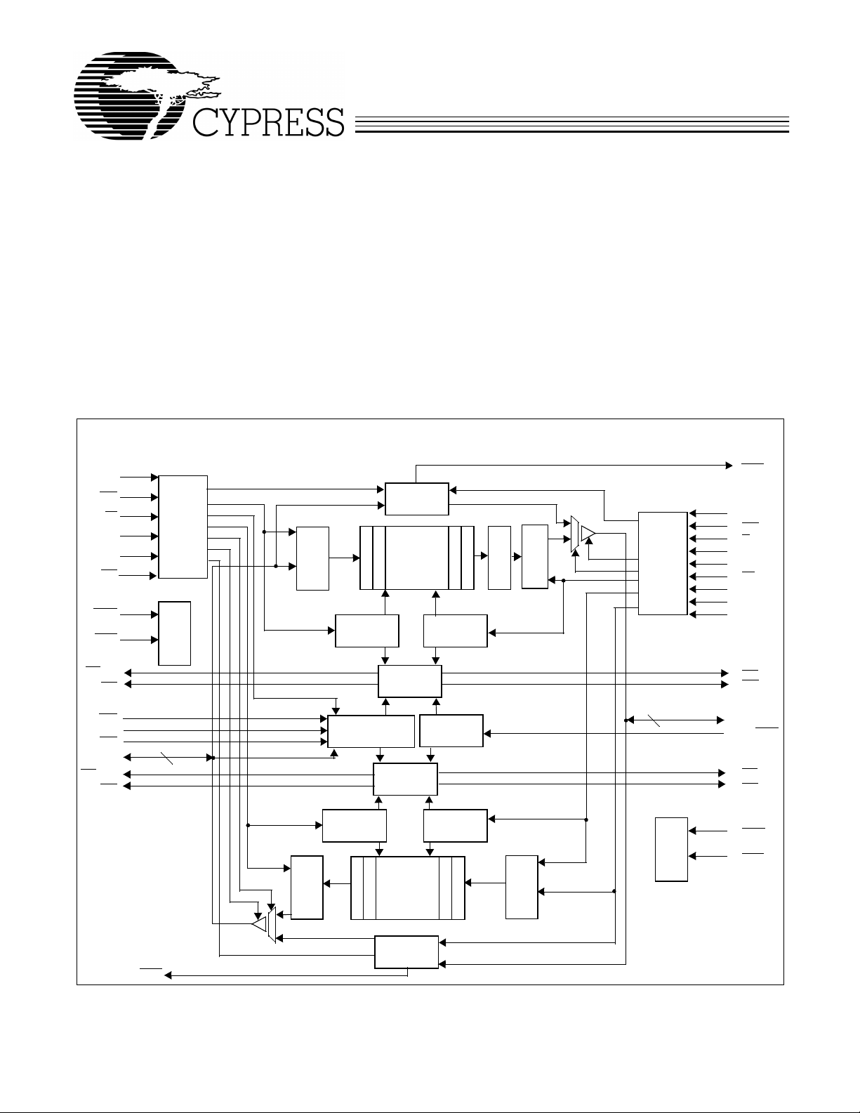
Logic Block Diagram
CY7C43644
CY7C43664
CY7C43684
1K/4K x36 x2 Bidirectional
• Fully asynchronous and simultaneous read and write
operation permitted
• Mailbox bypass reg ister for eac h FIFO
• Par allel and Serial Pro gram m able Almost-Full and
Almost-Empty flags
• Ret ra n smit func tion
• Standard or FWFT mode user selectable
• Partial Reset
• Big or Little Endian format for word or byte bus sizes
• 128-pin TQFP packaging
• Easily expandable in width and depth
CLKA
CSA
W/RA
ENA
MBA
RT2
MRS1
PRS1
FFA/IRA
AFA
SPM
FS0/SD
FS1/SEN
A
0–35
EFA/ORA
AEA
Port A
Control
Logic
FIFO1,
Mail 1
Reset
Logic
36
Input
Register
Programmable
Flag Offset
Registers
Output
Register
Write
Pointer
Write
Pointer
Mail 1
Register
1K/4K/16K
x36
Dual Ported
Memory
Status
Flag Logic
Status
Flag Logic
256/512/1K
4K/16K x36
Dual Ported
Memory
Read
Pointer
Timing
Mode
Read
Pointer
MBF1
CLKB
CSB
Port B
Control
Output
Register
Bus Matching
Logic
36
FIFO1,
Mail 1
Reset
Logic
Input
Register
W/RB
ENB
MBB
RTI
BE
BM
SIZE
EFB/ORB
AEB
B
0–35
BE/FWFT
FFB/IRB
AFB
MRS2
PRS2
MBF2
Cypress Semiconductor Corporation
Mail 2
Register
• 3901 North First Street • San Jose • CA 95134 • 408-943-2600
July 28, 2000
Page 2
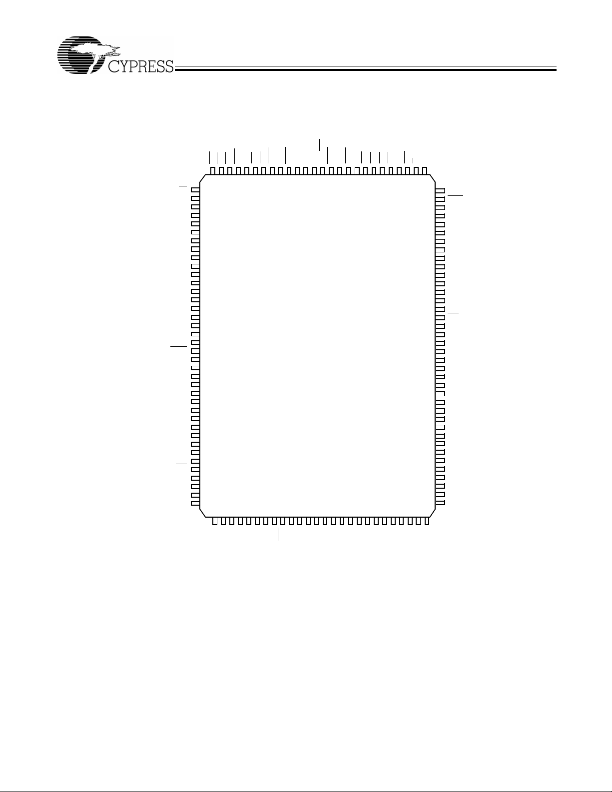
Pin Configuration
W/RA
ENA
CLKA
GND
A
A
A
A
V
A
A
GND
A
A
A
A
A
A
A
BE/FWFT
GND
A
V
A
A
A
A
GND
A
A
A
A
A
RT2
A
GND
A
A
CY7C43644
CY7C43664
CY7C43684
TQFP
Top View
AEA
AFA
MBF2
FS0/SD
MRS1
123
122
121
MBA
120
119
118
VCCPRS1
EFA/ORA
FFA/IRA
CSA
128
127
126
125
1
2
3
124
GND
117
GND
116
FS1/SEN
115
MRS2
114
MBB
113
112
VCCMBF1
111
AEB
110
4
5
35
6
34
33
7
32
8
9
CC
10
31
11
30
12
29
13
14
28
15
27
26
16
25
17
24
18
19
23
20
21
22
22
CC
23
21
24
20
25
19
26
18
27
28
17
29
16
30
15
31
14
32
13
33
34
12
35
36
11
37
10
38
CY7C43644
CY7C43664
CY7C43684
39404142434445464748495051525354555657585960616263
5
6A7A8A9
A
GND
2
A
A3A4A
CC
V
SPM
0
0A1
A
B
GND
AFB
109
GND
FFB/IRB
CSB
ENB
107
106
105
W/RB
104
102
101
100
103
99
98
97
96
95
94
93
92
91
90
89
88
87
86
85
84
83
82
81
80
79
78
77
76
75
74
73
72
71
70
69
68
67
66
65
CLKB
PRS2
V
CC
B
35
B
34
B
33
B
32
GND
GND
B
31
B
30
B
29
B
28
B
27
B
26
RT1
B
25
B
24
BM
GND
B
23
B
22
B
21
B
20
B
19
B
18
GND
B
17
B
16
SIZE
V
CC
B
15
B
14
B
13
B
12
GND
B
11
B
10
EFB/ORB
108
64
7
6
5B4B3B2B1
B
B
GND
B9B8B
CC
V
2
Page 3
CY7C43644
CY7C43664
CY7C43684
Functional Description
The CY7C436X4 is a monolithic, high-speed, low-power,
CMOS Bidirectional Synchronous (clocked) FIFO memory
which supports clock fr equencies up to 133 MHz and has read
access times as fast as 6 ns. Two independent 1K/4K/16K x
36 dual-port SRAM FIFOs on board each chip buffer data in
opposite directions. FIFO data on Port B can be input and
output in 36-bit, 18-bit, or 9-bit f ormats wit h a choice of Big or
Little Endian configurations.
The CY7C436X4 is a synchronous (clocked) FIFO, meaning
each port employs a synchronous interface. All data tr ansfers
through a port are gated to the LOW-to-HIGH transition of a
port clock by enable signals. The clocks for each port are independent of one another and can be asynchronous or coincident. The enables for each port are arranged to provide a
simple bidi rectional i nterfac e between microproces sors and/or
buses with synchronous control.
Communicat ion betw een ea ch port may b ypa ss the FIF Os vi a
two mailbox registers. The mailbox registers’ width matches
the selected P o rt B bus width. Each mailbo x registe r has a flag
(MBF1
and MBF2) to signal when new mail has been stored.
Two kinds of reset are available on the CY7C436X4: Master
Reset and P artial Reset. Mast er Reset init iali zes t he read and
write pointers to the first location of the memory array, configures the FIFO for Big or Little Endian byte arrangement and
selects serial f lag programmi ng, parallel flag pr ogramming, or
one of the three possible default flag offset settings, 8, 16, or
64. Each FIFO has its own independent Master Reset pin,
MRS1
and MRS2.
Partial Reset also sets the read and write pointers to the first
location of the mem ory. Unlike Master Rese t, any settings existing prior to P artial Reset ( i.e., pr ogr amming method a nd partial flag default offsets) are retained. Partial Reset is useful
since it permits fl ushing of the FI FO memory witho ut chang in g
any configuration settings. Each FIFO has its own, independent Partial Reset pin, PRS1
The CY7C436X4 have two modes of operation: In the CY
Standard Mode, the first word writt en to an empty FIFO is deposited into the memory array. A read operation is required to
access that word (along with all other words residing in memory). In the First-Word Fall-Through Mode (FWFT), the first
long-word ( 36-bit wide) written to an empty FIFO appears au-
and PRS2.
tomatically on the outputs, no read operation required (nevertheless, accessing subsequent words does necessitate a formal read request). The state of the BE/FWFT
operation det ermines th e mod e in use.
Each FIFO has a combined Empty/Output Ready flag (EFA
ORA and EFB
(FFA
/IRA and FFB/IRB). The EF and FF func tions are selected
in the CY Standard mode. EF
is full or not. The IR and OR functions are sele cted in the First Word F all -Through mode . IR indicates whet her or not the FIFO
has av ail able memory locations. OR shows whet her the FIFO
has data availab le for readi ng or not. It marks the presence of
valid data on the outputs.(See footnote #22)
Each FIFO has a programmable Alm ost Empty flag (AEA
AEB
) and a programmable Almost Full flag (AFA and AFB).
AEA
and AEB indic ate when a sele cted num ber of w ords written to FIFO memory achieve a predetermined “almost empty
state.” AFA
words written t o the m emory achieve a predet ermined “almost
full sta te.”(See footnote #44)
IRA, IRB, AFA
writes data into its array. ORA, ORB, AEA
chronized to th e port clock that reads data from its array. Programmable of fset f or AEA
in parallel using Port A or in serial via the SD input. Three
default offset settings are also provided. The AEA
threshold can be set at 8, 16, or 64 locations from the empty
boundary and AFA
64 locations from the full boundary. All these choi ces are made
using the FS0 and FS1 inputs during Master Reset.
Two or more devices may be used in parallel to create wider
data paths. If at any time the FI FO is not actively performing a
function, the chip will automatically power down. During the
power-down state, supply current consumption (I
minimum. Init iating a ny oper ati on (b y act iv ati ng con trol inputs )
will immediately take the device out of t he power-down st ate.
Retransmit feature is a vailable on these devices.
The CY7C436X4 are characterized for operation from 0
°C commercial, and from -40°
70
ESD protection is gr eater than 2001V, and latch -up is pr evented by the use of guard rings.
/ORB) and a combined Full/Input Ready flag
indicates whether the memory
and AFB indicate when a selected number of
, and AFB are synchroni zed to the port clock that
, AEB, AFA, and AFB can be loa ded
and AFB threshold can be set at 8, 16, or
C to 85
pin during F IFO
and
, and AEB are syn-
and AEB
) is at a
CC
°
°C industrial
C to
. Input
/
Selectio n Gu ide
CY7C43644/64/84
Maximum Frequency (MHz) 133 100 66.7
Maximum Access Time (ns) 6 8 10
Minimum Cycle Time (ns) 7.5 10 15
Minimum Data or Enable Set-Up (ns) 3 4 5
Minimum Data or Enabl e Hold ( ns) 0 0 0
Maximum Flag Delay (ns) 6 8 8
Active Power Supply
Current (I
Density 1K x 36 x2 4K x 36 x2 16K x 3 6 x 2
Package 128 TQFP 128 TQFP 128 TQFP
CC1
) (mA)
Commercial 100 100 100
Industrial 100
–7
CY7C43644 CY7C43664 CY7C43684
3
CY7C43644/64/84
–10
CY7C43644/64/84
15
−
Page 4
CY7C43644
CY7C43664
CY7C43684
Pin Definitions
Signal Name Description I/O Function
A
0–35
AEA
AEB
AFA
AFB
B
0–35
BE/FWFT
BM Bus Match
CLKA Port A Clock I CLKA is a continuous clock t hat synchr onizes al l data t ransf ers thr ough P ort A and can
CLKB Port B Clock I CLKB is a continuous clock t hat synchr onizes al l data t ransf ers thr ough P ort B and can
CSA
CSB
EFA
/ORA Port A Empty/
EFB
/ORB Port B Empty/
ENA Port A Enable I ENA must be HIGH to enable a LOW-to-HIGH transition of CLKA to read or write data
ENB Port B Enable I ENB must be HIGH to enable a LOW-to-HIGH transition of CLKB to read or write data
Port A Data I/O 36-bit bidirect ional data port for side A.
Port A Almost
Empty Flag
Port B Almost
Empty Flag
Port A Almost
Full Flag
Port B Almost
Full Flag
Port B Data I/O 36-bit bidirect ional data port for side B.
Big Endian/
First-Word FallThrough Select
Select (Port A)
Port A Chip
Select
Port B Chip
Select
Output Ready
Flag
Output Ready
Flag
O Programmab le Almost Empty flag sy nchronized to CLKA. It i s LOW whe n the number
of words in FIFO2 is less than or equal to the value in the Almost Empty A offset register,
X2. (See footnote #44.)
O Programmab le Almost Empty flag syn chronized to CLKB. It is LOW when the number
of words in FIFO1 is less than or equal to the value in the Almost Empty B offset register,
X1. (See footnote #44.)
O Programmab le Almost Full fl ag synchronized to CLKA. It i s LOW when the number of
empty locations in FIFO1 is less than or equal to the value in the Almost Full A offset
register, Y1. (See footnote #44.)
O Programmab le Almost Full flag synchronized to CLKB. It is LOW when the number of
empty locations in FIFO2 is less than or equal to the value in the Almost Full B offset
register, Y2. (See footnote #.)
I This is a dual-purpose pin. During Master Reset, a HIG H on BE will selec t Big Endian
operation. In thi s case, depe nding on the bus size, the most signi ficant byt e or word on
Port A is transferred to P ort B first for A-to-B data flow. For data flowing from Port B to
Port A the first word/byte written to Port B will come out as the most significant word/
byte on Port A. A LO W on BE will select Litt le Endian ope rati on. In th is case , the leas t
significant byte or word on Port A is tran s ferred to P o rt B fi rst fo r A-to-B d a ta flow.
Similarly , the fist word/byte written into P ort B will come out as the least significan t word/
byte on Po rt A for B-to-A data flow . After Master Reset, this pin selec ts the timing mode.
A HIGH on FWFT
mode. Once the timing mode has been selected, the level on this pin must be static
throughout device operation.
I A HIGH on this pin enables either b yte or wor d bus widt h on P ort B, depe nding on the
state of SIZE. A LOW select s long-word operation. BM works with SIZE and BE to
select the bus size and endian arrangement for Port B. The level of BM m ust be static
throughout device operation.
be asynchronous or coincident to CLKB. FFA
synchronized to the LOW-t o-HIGH transition of CLKA.
be asynchronous or coincident to CLKA. FFB
synchronized to the LOW-t o-HIGH transition of CLKB.
ICSA must be LOW to enable a LOW-to HIGH transition of CLKA to read or write on
Port A. The A
ICSB must be LOW to enable a LOW-to HIGH transition of CLKB to read or write on
Port B. The B
O This is a dual-function pin. In the CY Standard mode, the EFA
indicates whether or not the FIFO2 memory is empty. In the FWFT mode, the ORA
function is selected. ORA indicat es the presence o f valid data on A
able for reading. EFA
(See footnot e #22.)
O This is a dual-funct ion pin. In the CY Standard mode, the EFB
indicates whether or not the FIFO1 memory is empty. In the FWFT mode, the ORB
function is selected. ORB indicat es the presence o f valid data on B
able for reading. EFB
(See footnot e #22.)
on Port A.
on Port B.
selects CY St andard mode , a LOW se lects Fi rst- W ord Fall-Through
outputs are in the high-im pedance state when CSA is HIGH.
0–35
outputs are in the high- impedance state when CSB is HIGH.
0–35
/ORA is synchronized to the LOW-to-HIGH transition of CLKA.
/ORB is synchronized t o the LOW-to-HIGH transiti on of CLKB.
/IRA, EFA/ORA , A FA, and AEA are all
/IRB, EFB /ORB, AFB, and AEB are all
function is selected. EFA
outputs, avail-
0–35
function is selected. EFB
outputs, avail-
0–35
4
Page 5
CY7C43644
CY7C43664
CY7C43684
Pin Definitions
Signal Name Description I/O Function
/IRA Port A Full/Input
FFA
/IRB Port B Full/Input
FFB
FS1/SEN
FS0/SD Flag Offset
MBA P ort A Mailbox
MBB P ort B Mailbox
MBF1
MBF2
MRS1
MRS2
PRS1
PRS2
(continued)
Ready Flag
Ready Flag
Flag Offset
Select 1/Serial
Enable
Select 0/Serial
Data
Select
Select
Mail1 Register
Flag
Mail2 Register
Flag
FIFO1 Master
Reset
FIFO2 Master
Reset
FIFO1 Partial
Reset
FIFO2 Partial
Reset
O This is a dual-fun ction pin . In the CY Standar d mode, the FFA function is selected . FF A
indicates whether or not t he FIFO1 me mory is full. In t he FWFT mode , the IRA function
is selected. IRA indicat es whether or not there is space av ailable f or writing to the FIFO1
memory. FFA
O This is a dual-function pin. In the CY Standard mode, the FFB functio n is selected. FFB
indicates whether or not t he FIFO2 me mory is full. In t he FWFT mode , the IRB function
is selected. IRB indicat es whether or not there is space av ailable f or writing to the FIFO2
memory. FFB
I FS1/SEN
ming. During Master Reset, FS1/SEN
offset program ming method. Three offs et register progr amming methods are a vailab le:
automatically load one of three preset values (8, 16, or 64), parallel load f rom Port A,
I
or serial load. When serial load is selected for flag offset register pro gramming, FS1/
SEN
is used as an enab le synchron ous to the LO W- to-HIGH tr ansition of CLKA. When
FS1/SEN
and Y registers . The numbe r of bi t writes r equi red t o progr am t he off set re gister s is 4 0
for the CY7C43644, 48 for the CY7C43664, and 56 for the CY7C43684. The first bit
write stores the Y-register MSB and the last bit write stores the X-registe r LSB.
I A HIGH lev el on MBA chooses a mai lbox regis ter for a Port A read or write operation.
When a read operatio n is perf ormed on Port A, a HIGH le v el on MBA select s data from
the Mail2 register for output and a LOW lev el selects FIFO2 output register data fo r
output. When a write oper ati on is p erf ormed on Port A, a HIGH lev el on M BA wil l write
the data into Mail 1 register. While a LOW level will write the data into FIFO1.
I A HIGH lev el on MBB chooses a mai lbox regis ter for a Port B read or write operation.
When a read operatio n is perf ormed on Port B, a HIGH lev el on MBB select s data from
the Mail1 register for output and a LOW lev el selects FIFO1 output register data fo r
output. When a write oper ati on is per f ormed on Port B, a HIGH l ev e l on MBB wil l write
the data into Mail 2 register, while a LO W level will write the data into FIFO2.
OMBF1 is set LOW by a LOW-to-HI GH transition of CLKA that writes data to th e Mail1
register. Writes to the Mail1 register are inhibited whil e MBF1
HIGH by a LOW -t o-HIGH transition of CLKB when a Port B read is select ed and MBB
is HIGH. MBF1
OMBF2 is set LOW by a LOW-to-HI GH transition of CLKB that writes data to th e Mail2
register. Writes to the Mail2 register are inhibited whil e MBF2
HIGH by a LOW -t o-HIGH transition of CLKA when a Port A read is select ed and MBA
is HIGH. MBF2
I A LOW on this pin initiali zes the FIFO1 read and write pointers to the first locati on of
memory and sets the P ort B output register to al l zeroes . A LOW puls e on MRS1
the programmi ng method (serial or parallel ) and one of three p rogrammab le flag def ault
offsets f or FIFO1. It al so confi gures Port B for bus siz e and endian arr angem ent. F o ur
LOW-to-HIGH transitions of CLKA and four LO W-to-HIGH transitions of CLKB must
occur while MRS1
I A LOW on this pin initiali zes the FIFO2 read and write pointers to the first locati on of
memory and sets the P ort A output register to al l zeroes . A LOW puls e on MRS2
one of three programmable flag default offsets for FIFO2. Four LOW-to-HIGH transitions of CLKA and four LOW-t o-HIGH transitions of CLKB must occur while MRS2
LOW.
I A LOW on this pin initiali zes the FIFO1 read and write pointers to the first locati on of
memory and sets the Port B output register to all zeroes. Duri ng Partial Reset, the
currently selected bus size, endian arrangement, program ming method (serial or parallel), and progr am m able flag sett ings are all retained.
I A LOW on this pin initiali zes the FIFO2 read and write pointers to the first locati on of
memory and sets the Port A output register to all zeroes. Duri ng Partial Reset, the
currently selected bus size, endian arrangement, program ming method (serial or parallel), and progr am m able flag sett ings are all retained.
/IRA is synchroniz ed to the LOW-to-HIGH transition of CLKA.
/IRB is synchronized to the LOW -to-HIGH transition of CLKB.
and FS0/SD are dual-purpose input s used for flag off set register program-
and FS0/SD , together with SPM, sel ect the flag
is LOW, a rising edge on CLKA loads the bit present on FS0/SD into the X
is set HIGH following either a Master or Partial Reset of FIFO1.
is set HIGH following either a Master or Partial Reset of FIFO2.
is LOW.
is LOW. MBF1 is set
is LOW. MBF2 is set
selects
selects
is
5
Page 6
CY7C43644
CY7C43664
CY7C43684
Pin Definitions
(continued)
Signal Name Description I/O Function
RT1 Retransmit
FIFO1
I A LOW strob e on t his pi n will r etransmi t the d ata on FI FO1. Th is is achie ved by bri nging
the read point er back to loca tion zero . The user will still need to perform re ad operations
to retransmit the dat a. Retransmit func ti on applies to CY standard mode only.
RT2
Retransmit
FIFO2
I A LOW strobe on this pin will retransmit data on FIFO2. This is achieved by bringing
the read point er back to loca tion zero . The user will still need to perform re ad operations
to retransmit the dat a. Retransmit func ti on applies to CY standard mode only.
SIZE Bus Size Select I A HIGH on this pin when BM is HIGH selects byte bus (9-bit) size on Port B. A LOW
on this pin when BM is HIGH selec ts word (18-bit) bus size. SI ZE works with BM and
BE to select the bus size and endian arrangement for Port B. The level of SIZE must
be static throughout device operation.
SPM
W/RA
W/
RB Port B Write/
Maximum Ratings
(Abov e which the useful lif e m ay be impaired. For user guidelines, not tested.)
Storage Temperature ............. .......... ... .........–65
Ambient Temperature with
Power Applied ...............................................–55
Supply Voltage to Gr o u nd Potent ia l ..... ......... . –0.5V to +7.0V
DC Voltage Applied to Outp uts
in High Z State
DC Input Voltage
Notes:
1. Stresses beyond those listed under “Absolute Maximum Ratings” may cause permanent damage to the device. These are stress ratings only and functional
operation of the device at these or any other conditions beyond those indicated under “recommended operating conditions” is not implied. Exposure to absolutemaximum-rated conditions for extended periods may affect device reliability.
2. The input and output voltage ratings may be exceeded provided the input and output current ratings are observed.
3. Op erating V
Serial
Programming
Port A Write/
Read
Select
I A LOW on this pin se lects serial p rogrammin g of partial flag offs ets. A HIGH on t his pin
selects paral lel programming or default offsets (8, 16, or 64).
I A HIGH selects a write operation and a LOW selects a read operation on Port A for a
LOW-to-HIGH trans it ion of CLKA. The A
when W/RA
I A LOW selects a write operation and a HIGH sel ects a read operation on P ort B f or a
Read
Select
[1]
[2]
......................................–0.5V to VCC+0.5V
[2]
...................................–0.5V to VCC+0.5V
Range for -7 speed is 5.0V ±0.25V.
CC
LOW-to-HIGH transition of CLKB. The B
when W
/RB is LOW.
°
C to +150°C
°
C to +125°C
is HIGH.
outputs are in the high-impedance state
0–35
outputs are in the high-impedance state
0–35
Output Current into Outputs (LOW)............................. 20 mA
Static Discharge Voltage ........... .. ............ .. ................>2001V
(per MIL-STD-883, Method 3015)
Latch-Up Current .....................................................>200 mA
Operating Range
Ambient
Range
Temperature
Commercial 0°C to +70°C 5.0V ± 0.5V
Industrial –40°C to +85°C 5.0V ± 0.5V
[3]
V
CC
6
Page 7
CY7C43644
CY7C43664
CY7C43684
Electrical Characteristics
Over the Operating Range
Parameter Description T est Conditions
V
OH
V
OL
V
IH
V
IL
I
IX
I
OZL
I
OZH
[4]
I
CC1
[5]
I
SB
Capacitance
Output HIGH Voltage VCC = 4.5V,
I
= –4.0 mA
OH
Output LOW Voltage VCC = 4.5V,
I
= 8.0 mA
OL
Input HIGH Volt a g e 2.0 V
Input LOW Voltage –0.5 0.8 V
Input Leakage Current V
Output OFF, High Z
= Max. –10 +10 µA
CC
VSS < VO< V
Current
Active Power Supply
Current
Av erage Standby
Current
[6]
Parameter Description Test Conditions Max. Unit
C
C
IN
OUT
Input Capacitance TA = 25°C, f = 1 MHz ,
V
= 5.0V
Output Capacitance 8 pF
CC
CY7C43644/64/84
2.4 V
0.5 V
CC
–10 +10
Com’l 100 mA
Ind 100 mA
Com’l 10 mA
Ind 10 mA
4 pF
CC
UnitMin. Max.
V
µA
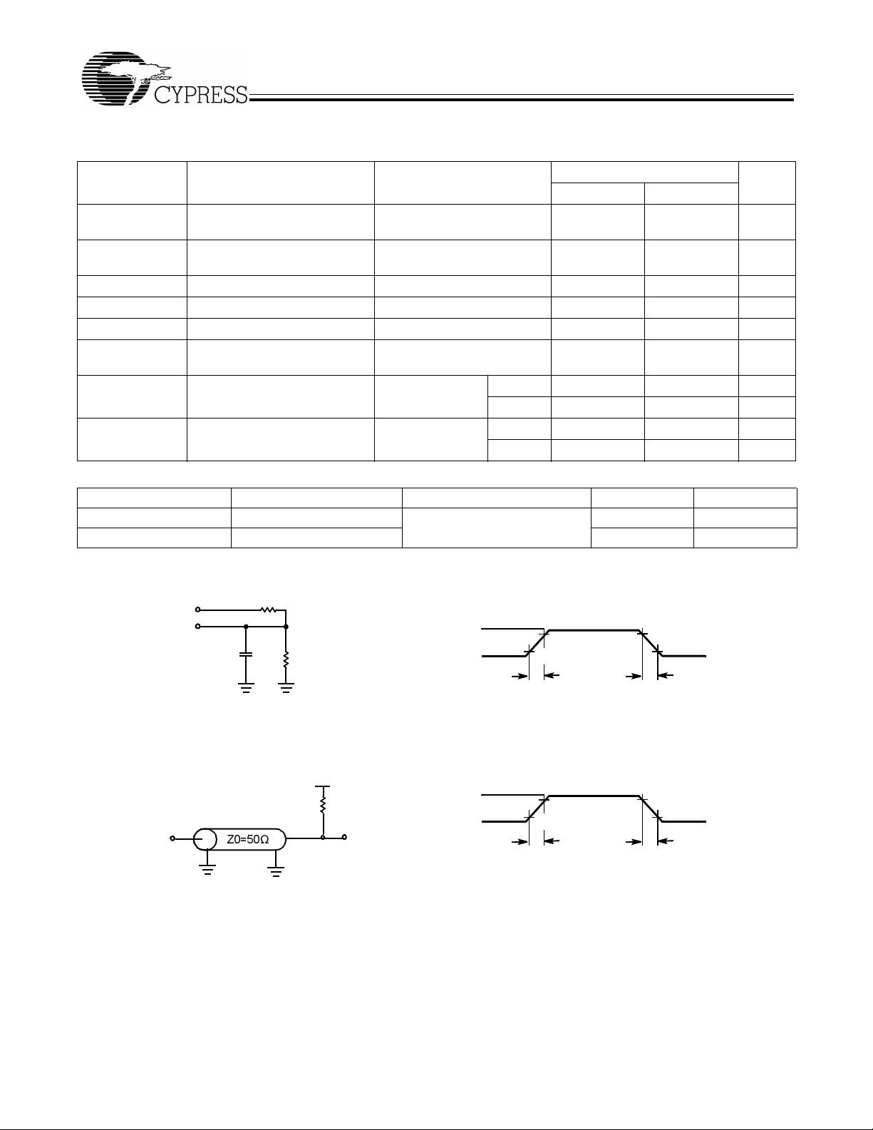
AC Test Loads and Waveforms (-10 & -15)
5V
OUTPUT
INCLUDING
R1=1.1K
CL=30 pF
JIG AND
SCOPE
Ω
R2=680
ALL INPUT PULSES
3.0V
Ω
GND
≤
3ns
90%
10%
90%
10%
3
ns
≤
AC Test Loads and Waveforms (-7)
VCC/2
50Ω
3.0V
GND
I/O
Notes:
4. Input signals switch from 0V to 3V with a rise/fall time of less than 3 ns, clocks and clock enables switch at 20 MHz, while data inputs switch at 10 MHz. Outputs
are unloaded.
5. All inputs = V
6. Tested initially and after any design or process changes that may affect these parameters.
– 0.2V, except RCLK and WCLK (which are at frequency = 0 MHz). All outputs are unloaded.
CC
=
Ω
≤
3ns
ALL INPUT PULSES
90%
10%
90%
10%
3
ns
≤
7
Page 8
CY7C43644
CY7C43664
CY7C43684
Switching Characteristics
Over the Operating Range
Parameter Description
f
S
t
CLK
t
CLKH
t
CLKL
t
DS
t
ENS
Clock Frequency, CLKA or CLKB 133 100 67 MHz
Clock Cycle Time, CLKA or CLKB 7.5 10 15 ns
Pulse Duration, CLKA or CLKB HIGH 3.5 4 6 ns
Pulse Duration, CLKA or CLKB LOW 3.5 4 6 ns
Set-Up Time, A
before CLKB↑
before CLKA↑ and B
0–35
Set-Up Time, CSA, W/R A, ENA, and MBA before
CLKA↑; CSB
, W/RB, ENB, and MBB before
CLKB↑
t
RSTS
t
FSS
t
BES
t
SPMS
t
SDS
t
SENS
t
FWS
t
DH
t
ENH
t
RSTH
t
FSH
t
BEH
t
SPMH
t
SDH
t
SENH
t
SPH
Set-Up Time, MRS1, MRS2, PRS1, or PRS2 LOW
before CLKA↑ or CLKB↑
[7]
Set-Up Time, FS0 and FS1 before MRS1 and
MRS2
HIGH
Set-Up Time, BE/FWFT before MRS1 and MRS2
HIGH
Set-Up Time, SPM befor e MRS1 and MRS2 HIGH 5 7 7.5 ns
Set-Up Time, FS0/SD before CLKA↑ 3 4 5 ns
Set-Up Time, FS1/SEN before CLKA↑ 3 4 5 ns
Set-Up Time, BE/FWFT before CLKA↑ 0 0 0 ns
Hold Time, A
CLKB↑
after CLK A↑ and B
0–35
Hold Time, CSA, W/RA, ENA, and MBA after
CLKA↑; CSB
Hold Time, MRS1, MRS2, PRS1, or PRS2 LOW
after CLKA↑ or CLKB↑
, W/RB, ENB, and MBB a fter CLKB↑
[7]
Hold Time, FS0 and FS1 after MRS1 and MRS2
HIGH
Hold Time, BE/FWFT after MRS1 and M RS2
HIGH
Hold Time, SPM after MRS1 and MRS2 HIGH 1 1 2 ns
Hold Time, FS0/SD after CLKA↑ 0 0 0 ns
Hold Time, FS1/SEN after CLKA↑ 0 0 0 ns
Hold Time, FS1/SEN HI GH after MRS1 and MRS2
HIGH
[8]
t
SKEW1
t
SKEW2
t
A
t
WFF
t
REF
Skew Time between CLKA↑ and CLKB↑ fo r E FA/
ORA, EFB
[8]
Skew Time betwe en CLKA↑ and CLKB↑ for AEA,
AEB
/ORB, FFA/IRA, and FFB/IRB
, AFA, AF B
Access Time, CLKA↑ to A
B
0–35
Propagation Delay Time, CLKA↑ to FFA/IRA and
CLKB↑ to FFB
/IRB
Propagation Dela y Time, CLKA↑ to EF A/ORA and
CLKB↑ to EFB
/ORB
and CLKB↑ to
0–35
0–35
0–35
after
CY7C43644/
64/84
–7
CY7C43644/
64/84
–10
CY7C43644/
64/84
–15
UnitMin. Max. Min. Max. Min. Max.
3 4 5 ns
3 4 5 ns
2.5 4 5 ns
6 7 7.5 ns
5 7 7.5 ns
0 0 0 ns
0 0 0 ns
1 2 4 ns
1 1 2 ns
1 1 2 ns
0 1 2 ns
5 5 7.5 ns
7 8 12 ns
1 6 1 8 3 10 ns
1 6 1 8 2 8 ns
1 6 1 8 1 8 ns
8
Page 9
CY7C43644
CY7C43664
CY7C43684
Switching Characteristics
Over the Operating Range (continued)
CY7C43644/
64/84
–7
CY7C43644/
64/84
–10
CY7C43644/
64/84
–15
Parameter Description
t
PAE
Propagation Delay Time, CLKA↑ to AEA and
1 6 1 8 1 8 ns
CLKB↑ to AEB
t
PAF
t
PMF
Propagation Delay Time, CLKA↑ to AFA and
CLKB↑ to AFB
Propagation Dela y Time, CLKA↑ to MBF1 LOW or
MBF2
HIGH and CLKB↑ to MBF2 LOW or MBF1
1 6 1 8 1 8 ns
0 6 0 8 0 12 ns
HIGH
t
PMR
t
MDV
t
RSF
t
EN
t
DIS
Propagation Delay Time, CLKA↑ to B
CLKB↑ to A
0–35
[10]
Propagation De lay Time , MBA to A
MBB to B
0–35
Valid
Propagation Dela y Time, MRS1 or PRS1 LO W to
AEB
LOW, AFA HIGH, FFA/IRA LOW, EFB/ORB
LOW and MBF1
to AEA
LOW, AFB HIGH, FFB/IRB LOW, EFA/
ORA LOW and MBF2
HIGH and MRS2 or PRS2 LOW
HIGH
Enable Time, CSA or W/RA LOW to A
and CSB
LOW and W/RB HIGH to B
Disable Time, CSA or W/RA HIGH to A
Impedance a nd CSB
HIGH or W/RB LOW to B
at High Impedance
t
PRT
t
RTR
Notes:
7. Requirement to count the clock edge as one of at least four needed to reset a FIFO.
8. Ske w time is not a timing constraint for proper device operation and is only included to illustrate the timing relationship between the CLKA cycle and the CLKB
cycle.
9. Writing data to the Mail1 register when the B
10. Writing data to the Mail2 register when the A
Retransmit Pulse W idt h 60 60 60 ns
Retransmit recovery Time 90 90 90 ns
outputs are active and MBB is HIGH.
0–35
outputs are active and MBA is HIGH.
0–35
0–35
Valid and
0–35
0–35
0–35
0–35
[9]
and
Active
Active
at High
0–35
1 7 2 11 3 12 ns
1 6 2 9 3 11 ns
1 6 1 10 1 15 ns
1 5 2 8 2 10 ns
1 5 1 6 1 8 ns
UnitMin. Max. Min. Max. Min. Max.
9
Page 10
Switching Waveforms
FIFO1 Master Reset Loading X1 and Y1 with a Preset Value of Eight
CLKA
CLKB
t
RSTS
[11, 12]
t
RSTH
CY7C43644
CY7C43664
CY7C43684
MRS1
t
BES
BE/FWFT
t
SPMS
SPM
t
FSS
FS1/SEN,
FS0/SD
FFA
/IRA
EFB
/ORB
t
t
t
RSF
RSF
RSF
AEB
t
RSF
AFA
t
RSF
MBF1
Notes:
11. Master Reset is performed in the same manner for FIFO2 to load X2 and Y2 with a preset value.
12. PRS1
must be HIGH during Master Reset.
BE
t
BEH
t
SPMH
t
FSH
t
FWS
FWFT
t
WFF
10
Page 11
CY7C43644
CY7C43664
CY7C43684
Switching Waveforms
FIFO1 Partial Reset (CY Stan dard and FW FT Mo des)
(continued)
[13, 14]
CLKA
CLKB
t
RSTS
t
RSTH
PRS1
t
RSF
FFA/IRA
t
RSF
EFB
/ORB
t
RSF
AEB
t
RSF
AFA
t
RSF
MBF1
Parallel Program ming of the Almost-Full Flag and Almost-Empty Flag Offset Values after Reset
(CY Standard and FWFT Modes)
[15]
t
WFF
CLKA
, MRS2
MRS1
SPM
t
FSS
t
FSS
t
t
FSH
FSH
FS1/SEN,
FS0/SD
FFA/
IRA
t
WFF
t
ENS
t
ENH
ENA
t
DH
DS
AEB Offset (X1)
AFB
Offset (Y2)
A
0 − 35
t
AFA Offset (Y1)
CLKB
FFB
/IRB
Notes:
13. Partial Reset is performed in the same manner for FIFO2.
14. MRS1
15. CSA=LOW, W/ RA=HIGH, MBA=LOW. It is not necessary to program offset register on consecutive clock cycles.
16. t
must be HIGH during Partial Reset.
is the minimum time between the rising CLKA edge and a rising CLKB for FFB/IRB to transition HIGH in the next cycle. If the time between the rising
SKEW1
edge of CLKA and rising edge of CLKB is less than t
, then FFB/IRB may transition HIGH one cycle later than shown.
SKEW1
AEA
t
SKEW1
Offset (X2)
[16]
First Word to FIFO1
t
WFF
11
Page 12
CY7C43644
CY7C43664
CY7C43684
Switching Waveforms
(continued)
Serial Programming of the Almost -Full Flag and Almost-Empty Flag
Offset Values (CY Standard and FWFT Modes)
[17]
CLKA
MRS1
,
MRS2
t
FSS
t
FSH
SPM
FFA/IRA
t
FSS
t
SPH
t
SENS
t
SENH
t
FS1/SEN
FS0/SD
[18]
t
SDS
AFA Offset (Y1) MSB
t
SDH
t
SDS
AEA Offset (X2) LSB
CLKB
FFB/
IRB
SENS
t
SENH
t
SKEW1
t
SDH
[16]
t
WFF
t
WFF
Port A Write Cycle Timing for FIFO1 (CY Standard and FWFT Modes)
t
t
CLKH
CLK
t
CLKL
CLKA
FFA/IRA
HIGH
t
ENS
t
ENH
CSA
t
t
ENH
ENS
W/RA
t
t
ENH
ENS
MBA
t
t
ENS
t
ENH
t
ENS
t
ENH
t
ENS
ENH
ENA
t
t
DS
DH
A
0–35
Notes:
17. It is not necessary to program offset register bits on consecutive clock cycles. FIFO write attempts are ignored until IRA is set HIGH.
18. Programmable offsets are written serially to the SD input in the order AFA
19. Written to FIFO1.
W1
[19]
offset (Y1), AEB offset (X1), AFB offset (Y2), and AEA offset (X2).
W2
[19]
12
Page 13

CY7C43644
CY7C43664
CY7C43684
Switching Waveforms
(continued)
Port B Long-Word Write Cycle Timing for FIFO2 (CY Standard and FWFT Modes)
t
CLKH
CLK
t
CLKL
t
CLKB
/IRB
FFB
HIGH
t
ENS
t
ENH
CSB
t
t
ENH
ENS
W/RB
t
t
ENS
ENH
MBB
t
ENS
t
ENH
t
ENS
t
ENH
ENB
t
t
DS
B
0−35
W1
[20]
DH
W2
[20]
t
ENStENH
Port B W ord Write Cycle Ti ming for FIFO2 (CY Standard and FWFT Modes)
CLKB
/IRB
FFB
HIGH
t
ENS
CSB
t
ENS
W/RB
t
ENStENH
MBB
t
ENS
t
ENH
t
ENS
ENB
t
B
0–17
Note:
20. Written to FIFO2.
DStDH
t
ENH
t
ENH
13
Page 14

CY7C43644
CY7C43664
CY7C43684
Switching Waveforms
(continued)
Port B Byte Write Cycle Timing for FIFO2 (CY Standard and FWFT Modes)
CLKB
/IRB
FFB
HIGH
t
ENS
CSB
t
ENS
W/RB
t
t
ENS
ENH
MBB
t
t
ENH
ENS
ENB
t
t
DS
DH
B
0–8
t
ENS
t
t
ENH
t
ENH
ENH
Port B Long-Word Read Cycle Timing for FIFO1 (CY Standard and FWFT Modes)
t
CLK
t
CLKH
t
CLKL
CLKB
EFB
/ORB
HIGH
CSB
W/RB
MBB
t
ENS
t
ENH
t
ENS
t
ENH
ENB
B
0–35
(Standard Mode)
OR
B
0–35
(FWFT Mode)
W1
[21]
t
A
[21]
W1
t
A
[21]
W2
t
MDV
t
EN
t
MDV
t
EN
Previous Data
t
A
t
A
[22]
t
ENS
No Operation
[21]
W2
[21]
W3
t
ENH
t
DIS
t
DIS
Note:
21. Read from FIFO1.
22. When reading from the FIFO under FWFT, ORA/ORB signal should be included in the read logic to ensure proper operation. To read without gating the
boundary flag (e.q. in bursts), use CY standard mode.
14
Page 15

CY7C43644
CY7C43664
CY7C43684
Switching Waveforms
(continued)
Port B Word Read Cycle Timing for FIFO1 (CY Standard and FWFT Modes)
CLKB
/ORB
EFB
CSB
W/RB
MBB
t
t
ENH
ENS
ENB
B
0–17
(Standard Mode)
OR
B
0–17
(FWFT Mode)
t
t
MDV
MDV
t
EN
t
EN
t
A
Previous Data
t
A
Read 1
Read 1
Read 2
[22, 24]
t
A
t
A
No Operation
Read 2
Read 3
t
DIS
t
DIS
Port B Byte Read Cycle Timing f or FIFO1 (CY Standard and FWFT Modes)
CLKB
/ORB
EFB
HIGH
CSB
W/RB
MBB
t
t
ENS
ENH
ENB
Read 1
t
Read 2
t
A
A
Read 2
Read 3
t
A
t
A
B
0–8
(Standard Mode)
OR
B
0–8
(FWFT Mode)
Notes:
23. Unused word B
24. Unused bytes B
t
MDV
t
EN
Previous Data
t
MDV
t
EN
Read 1
contains all zeroes for word-size reads.
18–35
, B
9–17
18–26
, and B
contain all zeroes for byte-size reads.
27–35
t
A
t
A
[22, 23]
Read 3
Read 4
t
A
t
A
No Operation
Read 4
Read 5
t
DIS
t
DIS
15
Page 16

CY7C43644
CY7C43664
CY7C43684
Switching Waveforms
(continued)
Port A Read Cycle Timing for FIFO2 (CY Standard and FWFT Modes)
t
CLK
t
CLKH
t
CLKL
CLKA
/ORA
EFA
HIGH
CSA
W/RA
MBA
t
t
ENS
ENH
ENA
W1
[25]
t
A
W1
t
A
W2
A
0−35
(Standard Mode)
OR
A
0−35
(FWFT Mode)
t
MDV
t
EN
t
MDV
t
EN
Previous Data
[25]
[25]
t
ENS
[22]
t
ENH
t
ENStENH
t
A
t
A
No Operation
[25]
W2
[25]
W3
t
t
DIS
DIS
Note:
25. Read from FIFO2.
16
Page 17

CY7C43644
CY7C43664
CY7C43684
Switching Waveforms
(continued)
ORB Flag Timing and First Data Word Fall Through when FIFO1 is Empty (FWFT Mode)
t
CLK
t
t
CLKH
CLKL
CLKA
CSA
W/RA
LOW
HIGH
t
ENS
t
ENH
MBA
t
t
ENS
ENH
ENA
FFA
A
0–35
CLKB
EFB
/IRA
/ORB
HIGH
FIFO1 Empty
t
t
DH
DS
W1
[27]
t
t
SKEW
CLKH
t
CLK
t
CLKL
t
REF
t
[22, 26]
REF
CSB
W/RB
MBB
LOW
HIGH
LOW
ENB
t
A
B
0–35
Notes:
26. If Port B size is word or byte, EFB
27. t
is the minimum time between a rising CLKA edge and a rising CLKB edge for ORB to transition HIGH and to clock the next word to the FIFO1 output
SKEW1
register in three CLKB cycles. If the time between the rising CLKA edge and rising CLKB edge is less than t
load of the first word to the output register may occur one CLKB cycle later than shown.
Old Data in FIFO1 Output Register
is set LOW by the last word or byte read from FIFO1, respectively.
t
ENStENH
W1
, then the transition of ORB HIGH and
SKEW1
17
Page 18

CY7C43644
CY7C43664
CY7C43684
Switching Waveforms
(continued)
EFB Flag Timing and First Data Read Fall Through when FIFO1 is Empty (CY standard Mode)
t
CLK
t
t
CLKH
CLKL
CLKA
CSA
W/RA
LOW
HIGH
t
ENS
t
ENH
MBA
t
t
ENS
ENH
ENA
/IRA
FFA
A
0–35
HIGH
t
DS
W1
t
DH
t
SKEW1
[28]
t
CLKH
t
CLKL
CLKB
t
REF
EFB
/ORB
FIFO1 Empty
t
CLK
t
REF
[26]
CSB
W/RB
MBB
LOW
HIGH
LOW
ENB
B
0–35
Note:
28. t
is the minimum time between a rising CLKA edge and a rising CLKB edge for EFB to transition HIGH in the next CLKB cycle. If the time between
SKEW1
the rising CLKA edge and rising CLKB edge is less than t
t
t
ENS
ENH
t
A
W1
, then the transition of EFB HIGH may occur one CLKB cycle later than shown.
SKEW1
18
Page 19

CY7C43644
CY7C43664
CY7C43684
Switching Waveforms
(continued)
ORA Flag Timing and First Data Word F all Through when FIFO2 is Empty (FWFT Mode)
t
CLK
t
CLKHtCLKL
CLKB
CSB
W/RB
LOW
LOW
t
ENS
t
ENH
MBB
t
t
ENH
ENS
ENB
FFB
B
0–35
/IRB
HIGH
t
W1
t
DH
DS
[30]
t
CLKHtCLKL
t
SKEW1
CLKA
t
REF
EFA
/ORA
FIFO2 Empty
t
CLK
t
[22, 29]
REF
CSA
W/RA
MBA
LOW
LOW
LOW
ENA
t
A
A
0–35
Notes:
29. If Port B size is word or byte, t
30. t
is the minimum time between a rising CLKB edge and a rising CLKA edge for ORA to transition HIGH and to clock the next word to the FIFO2 output
SKEW1
register in three CLKA cycles. If the time between the rising CLKB edge and rising CLKA edge is less than t
load of the first word to the output register may occur one CLKA cycle later than shown.
Old Data in FIFO2 Output Register
is referenced to the rising CLKB edge that writes the last word or byte of the long-word, respectively.
SKEW1
t
ENStENH
W1
, then the transition of ORA HIGH and
SKEW1
19
Page 20

CY7C43644
CY7C43664
CY7C43684
Switching Waveforms
(continued)
EFA Flag Timing and First Data Read when FIFO2 is Empty (CY Standard Mode)
t
CLK
t
CLKHtCLKL
CLKB
CSB
W/RB
LOW
LOW
t
ENS
t
ENH
MBB
t
t
ENH
ENS
ENB
FFB
B
0–35
/IRB
HIGH
t
DS
W1
t
DH
t
SKEW1
[31]
t
CLKHtCLKL
CLKA
t
REF
EFA
/ORA
FIFO2 Empty
t
CLK
t
REF
[29]
CSA
W/RA
MBA
LOW
LOW
LOW
ENA
A
0–35
Note:
31. t
is the minimum time between a rising CLKB edge and a rising CLKA edge for EFA to transition HIGH in the next CLKA cycle. If the time between the
SKEW1
rising CLKB edge and rising CLKA edge is less than t
t
ENStENH
t
A
W1
, then the transition of EFA HIGH may occur one CLKA cycle later than shown.
SKEW1
20
Page 21

CY7C43644
CY7C43664
CY7C43684
Switching Waveforms
(continued)
IRA Flag Timing and First Available Write when FIFO1 is Full (FWFT Mode)
t
CLK
t
t
CLKH
CLKL
CLKB
CSB
W/RB
LOW
HIGH
MBB
t
t
ENH
ENS
ENB
EFB
B
/ORB
0–35
HIGH
t
A
Previo us Word in FI FO1 Outp ut Register
t
SKEW1
Next Word From FIFO1
[32]
t
CLKHtCLKL
CLKA
t
WFF
FFA
/IRA
FIFO1 Full
t
CLK
t
WFF
[29]
CSA
W/RA
LOW
HIGH
MBA
ENA
A
0–35
Note:
32. t
is the minimum time between a rising CLKB edge and a rising CLKA edge for IRA to transition HIGH in the next CLKA cycle. If the time between the
SKEW1
rising CLKB edge and rising CLKA edge is less than t
t
t
ENS
ENH
t
ENStENH
t
t
DS
DH
To FIFO1
, then IRA may transition HIGH one CLKA cycle later than shown.
SKEW1
21
Page 22

CY7C43644
CY7C43664
CY7C43684
Switching Waveforms
(continued)
FFA Flag Timing and Fi rst Av ailable Write when FIFO1 is Full (CY Standard Mode)
t
CLK
t
t
CLKH
CLKL
CLKB
CSB
W/RB
MBB
LOW
HIGH
LOW
t
ENStENH
ENB
/ORB
EFB
B
0–35
HIGH
t
A
Previous Word in FIFO1 Output Register
t
SKEW1
Next Word From FIFO1
[33]
t
CLKH
t
CLKL
CLKA
t
WFF
FFA
/IRA
FIFO1 Full
t
CLK
t
WFF
[29]
CSA
W/RA
LOW
HIGH
MBA
ENA
A
0−35
Note:
33. t
is the minimum time between a rising CLKB edge and a rising CLKA edge for FFA to transition HIGH in the next CLKA cycle. If the time between the
SKEW1
rising CLKB edge and rising CLKA edge is less than t
t
t
ENH
ENS
t
t
ENS
ENH
tDHt
DS
, then the transition of FFA HIGH may occur one CLKA cycle later than shown.
SKEW1
22
Page 23

CY7C43644
CY7C43664
CY7C43684
Switching Waveforms
(continued)
IRB Flag Timing and First Available Write when FIFO2 is Full (FWFT Mode)
t
CLK
t
t
CLKH
CLKL
CLKA
CSA
W/RA
MBA
LOW
LOW
LOW
t
ENS
t
ENH
ENA
EFA
A
0–35
/ORA
HIGH
tA
Previous Word in FIFO2 Output Register
t
SKEW1
Next Word From FIFO2
[35]
t
CLKH
t
CLKL
CLKB
t
WFF
FFB
/IRB
FIFO2 Full
t
CLK
t
WFF
[34]
CSB
W/RB
LOW
LOW
t
ENS
t
ENH
MBB
t
t
ENH
ENS
ENB
tDHt
DS
B
0–35
To FIFO2
Notes:
34. If Port B size is word or byte, IRB is set LOW by the last word or byte write of the long-word, respectively.
35. t
is the minimum time between a rising CLKA edge and a rising CLKB edge for IRB to transition HIGH in the next CLKB cycle. If the time between the
SKEW1
rising CLKA edge and rising CLKB edge is less than t
, then the transition of IRB HIGH may occur one CLKB cycle later than shown.
SKEW1
23
Page 24

CY7C43644
CY7C43664
CY7C43684
t
CLK
t
(continued)
CLKL
Switching Waveforms
FFB Flag Timing and Firs t Available Write when FIFO2 is Full (CY Standard Mode)
t
CLKH
CLKA
CSA
W/RA
MBA
LOW
LOW
LOW
t
ENS
t
ENH
ENA
EFA
A
0–35
/ORA
HIGH
t
A
Previous Word in FIFO12 Output Register
t
SKEW1
Next Word From FIFO2
[37]
t
CLKH
t
CLKL
CLKB
t
WFF
FFB
/IRB
FIFO2 Full
t
CLK
t
WFF
[36]
CSB
W/RB
LOW
LOW
MBB
ENB
B
0–35
Notes:
36. If Port B size is word or byte, FFB
37. t
is the minimum time between a rising CLKA edge and a rising CLKB edge for FFB to transition HIGH in the next CLKB cycle. If the time between the
SKEW1
rising CLKA edge and rising CLKB edge is less than t
is set LOW by the last word or byte write of the long-word, respectively.
t
t
ENS
ENH
t
ENStENH
tDHt
DS
To FIFO2
, then the transition of FFB HIGH may occur one CLKB cycle later than shown.
SKEW1
24
Page 25

CY7C43644
CY7C43664
CY7C43684
Switching Waveforms
Timing for AEB
CLKA
ENA
CLKB
AEB
ENB
Timing for AEA
CLKB
ENB
CLKA
AEA
ENA
when FIFO2 is Almost Empty (CY Standard and FWFT Modes)
X1 Word in FIFO1
when FIFO2 is Almost Empty (CY Standard and FWFT Modes)
X2 Word in FIFO2
(continued)
t
ENS
t
ENS
t
ENH
t
SKEW2
t
ENH
t
SKEW2
[40]
[43]
t
PAE
t
PAE
[38, 39, 44]
(X1+1)Words in FIFO2
t
ENS
[41, 42, 44]
(X2+1) Words in FIFO2
t
ENS
t
PAE
t
ENH
t
PAE
t
ENH
Notes:
38. FIFO1 Write (CSA
read from the FIFO.
39. If Port B size is word or byte, AEB
40. t
41. FIFO2 Write (CSB = LOW, W/RB = LOW, MBB = LOW), FIFO2 Read (CSA = LOW, W/RA = LOW, MBA = LOW). Data in the FIFO2 output register has been
42. If Port B size is word or byte, t
43. t
44. When FIFO is operated at the almost empty/full boundary, there may be an uncertainty of up to 3 clock cycles for flag assertion and deassertion. Refer to
is the minimum time between a rising CLKA edge and a rising CLKB edge for AEB to transition HIGH in the next CLKB cycle. If the time between
SKEW2
the rising CLKA edge and rising CLKB edge is less than t
read from the FIFO.
is the minimum time between a rising CLKB edge and a rising CLKA edge for AEA to transition HIGH in the next CLKA cycle. If the time between
SKEW2
the rising CLKB edge and rising CLKA edge is less than t
“Designing with CY7C436xx Synchronous FIFO” application notes for more details on flag uncertainties.
= LOW, W/RA = LOW, MBA = LOW), FIFO1 Read (CSB = LOW , W/RB = HIGH, MBB = LOW). Data in the FIFO1 output register has been
is set LOW by the last word or byte read from FIFO1, respectively.
, then AEB may transition HIGH one CLKB cycle later than shown.
SKEW2
is referenced to the rising CLKB edge that writes the last word or byte of the long word, respectively.
SKEW2
, then AEA may transition HIGH one CLKA cycle later than shown.
SKEW2
25
Page 26

CY7C43644
CY7C43664
CY7C43684
Switching Waveforms
(continued)
Timing for AFA when FIFO1 is Almost Full (CY Standard and FWFT Modes)
[46]
t
CLKA
ENA
AFA
t
ENS
t
t
PAF
ENH
[D–(Y1+1)] Words in FIFO 1
(D–Y1)Words in FIFO1
SKEW2
CLKB
t
ENB
Timing for AFB
CLKB
ENB
t
when FIFO2 is Almost Full (CY Standard and FWFT Modes)
t
t
ENS
ENH
ENS
ENH
t
SKEW2
[48]
[38, 42, 44, 45]
[41, 44, 45 , 47 ]
t
PAF
AFB
[D–(Y2+1)] Words in FIFO2
t
PAF
(D–Y2)Words in FIFO2
CLKA
t
t
ENA
Notes:
45. D = Maximum FIFO Depth = 1K for the CY7C43644, 4K for the CY7C43664, and 16K for the CY7C43684.
46. t
47. If Port B size is word or byte, AFB is set LOW by the last word or byte write of the long word, respectively .
48. t
is the minimum time between a rising CLKA edge and a rising CLKB edge for AFA to transition HIGH in the next CLKA cycle. If the time between the
SKEW2
rising CLKA edge and rising CLKB edge is less than t
is the minimum time between a rising CLKB edge and a rising CLKA edge for AFB to transition HIGH in the next CLKB cycle. If the time between
SKEW2
the rising CLKB edge and rising CLKA edge is less than t
ENS
, then AFA may transition HIGH one CLKB cycle later than shown.
SKEW2
, then AFB may transition HIGH one CLKA cycle later than shown.
SKEW2
ENH
t
PAF
26
Page 27

CY7C43644
CY7C43664
CY7C43684
Switching Waveforms
(continued)
Timing for Mail1 Register and MBF1
CLKA
CSA
t
W/RA
MBA
ENA
A
0–35
CLKB
MBF1
CSB
Flag (CY Standard and FWFT Modes)
t
t
ENH
ENS
t
ENS
t
ENS
t
ENS
t
DS
W1
ENH
t
ENH
t
ENH
t
DH
t
PMF
[49]
t
PMF
W/RB
MBB
ENB
t
EN
FIFO1 Output Register
Note:
49. If Port B is configured for word size, data can be written to the Mail1 register using A
valid data (B
inputs). In this second case, B
will be indeterminate). If Port B is configured for byte size, data can be written to the Mail1 Register using A
18–35
will have valid data (B
0–8
t
MDV
will be indeterminate).
9–35
t
PMR
t
ENS
W1 (Remains valid in Mail1 Register after read)
(A
0–17
are “don’t care” inputs). In this first case B
18–35
t
ENH
0–8
t
DIS
(A
are “don’t care”
9–35
0–17
will have
27
Page 28

CY7C43644
CY7C43664
CY7C43684
Switching Waveforms
(continued)
Timing for Mail2 Register and MBF2 Flag (CY Standard and FWFT Modes)
CLKB
t
t
ENH
ENS
CSB
t
t
ENH
ENS
W/RB
t
t
ENH
ENS
MBB
t
t
ENH
ENS
ENB
t
t
DH
DS
B
0–35
W1
CLKA
t
PMF
MBF2
CSA
[50]
t
PMF
W/RA
MBA
t
ENS
t
ENH
ENA
t
MDV
t
PMR
W1 (Remains valid in Mail2 Register after read)
A
0−35
FIFO1 Retransmit Timing
t
EN
FIFO2 Output Register
[51, 52, 53, 54]
RT1
t
PRT
t
RTR
ENB
EFB/FFA
Notes:
50. If Port B is configured for word size, data can be written to the Mail2 register using B
valid data (A
inputs). In this second case, A
51. Retransmit is performed in the same manner for FIFO2.
52. Clocks are free-running in this case. CY standard mode only.
53. The flags may change state during Retransmit as a result of the offset of the read and write pointers, but flags will be valid at t
54. For the AEA, AEB, AFA and AFB flags, two clock cycles are necessary after t
will be indeterminate). If Port B is configured for byte size, data can be written to the Mail2 Register using B
18–35
will have valid data (A
0–8
will be indeterminate).
9–35
rtr
(B
0–17
to update these flags
are “don’t care” inputs). In this first case A
18–35
0–8
RTR
t
DIS
(B
are “don’t care”
9–35
.
0–17
will have
28
Page 29

CY7C43644
CY7C43664
CY7C43684
Signal Description
Master Reset (MRS1, MRS2)
Each of the two FIFO memories of the CY7C436X4 undergoes
a complete reset by taking its associated Master Reset
, MRS2) i nput LOW for a t least f our P ort A clock ( CLKA)
(MRS1
and four Port B clock (CLKB) LOW-to-HIGH transitions. The
Master Reset inputs can s witch asynchronously to the cl ocks.
A Master Reset initializes the internal read and write pointers
and forc es the Full/ Input Ready fl ag (FF A
the Empty/Output Ready flag (EF A
Almost Empty flag (AEA
(AFA
, AFB) HIGH. A Master Reset also forces the Mailbox f lag
(MBF1
, MBF2) of the parallel mailbox register HIGH. After a
Master Reset, the FIFO’s Full/Input Ready flag is set HIGH
after tw o cloc k cycle s to begin normal oper ati on. A Master Reset must be pe rformed on t he FIFO a fter po wer up , bef ore data
is written to its memory.
A LOW-to-HIGH transition on a FIFO Master Reset (MRS1
MRS2
) input latches t he value of the Big Endian (BE) input or
determining the order by which bytes are transferred through
Port B.
A LOW-to-HIGH transition on a FIFO reset (MRS1
input latches the v alues of the Flag select (FS0, FS1) and Serial Programming Mode (SPM
Full and Almost Empty offset programming method (see Almost Empty and Almost Full flag offset programming below).
Partial Reset (PRS1
Each of the two FIFO memories of the CY7C436X4 undergoes
a limited reset by taking its associated Partial Reset (PRS1
PRS2
) input LO W f or at least four Port A clock ( CLKA) and f our
Po rt B clock (CLKB) LOW -to-HIGH trans itions. The Partial Reset inputs can switch asynchronously to the clocks. A Partial
Reset initial izes the int ernal read and write pointer s and for ces
the Full/Input Ready flag (FF A
Output Ready flag (EFA
Empty flag (AEA
AFB
) HIGH. A Partial Reset also forces the Mailbox flag
(MBF1
, MBF2) of the parallel mailbox register HIGH. After a
Partial Reset, the FIFO’s Full/Input Ready flag is set HIGH
after two cl ock cycles to begin normal operation.
Whatev er flag offset s, progr amming method (paral lel or serial),
and timing mode (FWFT or CY Standard mode) are currently
selected at the time a Partial Reset is initiated, those settings
will remain unch anged upon c ompletion of the reset operation.
A Partial Reset may be useful in the case where reprogramming a FIFO following a Master Reset would be i nconveni ent.
Big Endian/First-Word Fall-Through (BE/FWFT
This is a dual-purpose pin. At the time of Master Reset , the BE
select function is active, permitting a choice of big or little endian byte arrangement for data written to or read from Port B.
This select ion determines the order by which bytes (or words)
of data ar e tr ans fe rred thr ough t his po rt. Fo r the followi ng illustrations, assume that a byte (or word) bus size has been selected for Port B. (Note that when Port B is configured for a
long-word siz e, th e Big Endian functio n has no application and
the BE input is a “don’t care”.)
A HIGH on the BE/FWFT
and MRS2) inputs go f rom LOW to HIGH will select a Big Endian arrangement. When data is moving in the direction from
Port A to Port B, the most significant byte (word) of the long
, AEB) LOW, and the Almost Full flag
) inputs f or choosing the Almost
, PRS2)
/IRA, FFB/IRB) LO W , the Empty/
/ORA, EFB/ORB) LOW, the Almost
, AEB) LOW, and the Almost Full flag (AFA,
input when the M aster Reset (M RS1
/IRA, FFB/IRB) LOW,
/ORA, EFB/ORB) LO W, the
, MRS2)
)
word written to P ort A will be transferred to P ort B first; the least
significant b yte (word) of the lon g-word written to P ort A will be
transf erred t o P ort B la st. When dat a is mo vi ng in th e direc tion
from Port B to Port A, the byte (word) written to Port B first will
be transferred to Port A as the most significant byte (word) of
the long-word; the byte (word) written to Port B last will be
transferred to Port A as the least significant byte (word) of the
long word.
A LOW on the BE/FWFT
and MRS2) inputs go from LOW to HIGH will select a Little
Endian arrangement. When data is moving in the direction
from Port A to Port B, the least significant byte (word) of the
long-word written to Port A will be transferred to Port B first;
the most signi ficant b yte (wor d) of the long -word writ ten to P ort
A will be transferred to Port B last. When data is moving in the
direction from Port B to Port A, the byte (word) written to Por t
B first will be transferred to Port A as the least significant byt e
(word) of the long-word; the byte (word) written to Port B last
will be transf er red to P ort A as the most signif icant byt e (word )
,
of the long-word.
After Master Reset, t he FWFT select func tion is activ e, permit-
ting a choice between two possible timing modes: CY Standard mode or First-Word Fal l-Through (FWFT) mode. Once
the Master R eset (MRS 1
BE/FWFT
CLKA (for FIFO1) and CLKB (for FIFO2) will select CY Standard mode. This mode uses the Empty Flag function (EFA
EFB
the FIFO memory. It uses the Full Flag function (FFA
indicate whether or not the FIFO memory has any free space
for writing. In CY Standard mode, every word read from the
,
FIFO, including the first, must be requested using a formal
read operation.
Once the Master Reset (MRS1
on the BE/FWFT
sition of CLKA (for FIFO1) and CLKB (for FIFO2) will select
FWFT mode. This mode uses the Output Ready function
(ORA, ORB) to indicate whether or not there is valid data at
the data outputs (A
function (IRA, IRB) to indicate whether or not the FIFO memory has any free space f or writing . In the FWFT mode, the fi rst
word written to an empty FIFO goes directly to data outputs,
no read request necessary. Subsequent words must be accessed by performing a formal read oper ation.
Following Master Reset, the level applied to the BE/FWFT
put to choose the desired timing mode must remain static
throughout the FIFO ope ration.
Programming the Almost Empty and Almos t Full Flags
Four registers in the CY7C436X4 are used to hold the offset
values for the Al m ost Empty and Al most Full flags . The Port B
Almost Empty flag (AEB
Port A Almost Empty flag (AEA
The Port A Almost Full flag (AFA
and the Port B Almost Full flag (AFB
Y2. The index of each register name corresponds with preset
values during the reset of a FIFO, programmed in parallel using the FIFO’s Port A data inputs, or programmed in serial
using the Serial Data (SD) input (see Table 1).
To load a FIFO’s Almost Empty fla g and Almost Ful l flag of fset
registers with one of the three preset values listed in Table 1,
the Serial Program Mode (SPM
select inp uts must be HIG H during t he LO W -to-HIGH transiti on
of its Master Reset input (MRS1
input at the second LOW-to-HIGH transition of
) to indicat e whether or not t here ar e a ny wo rds present in
input when the Master Reset (MRS1
, MRS2) input is HIGH, a HIGH on the
,MRS2) input is HIGH, a LOW
input during the second LOW-to-HIGH tran-
0–35
or B
). It also uses t he Input Ready
0–35
) offset register is labeled X1 and the
) offset register is labeled X2.
) offset register is labeled Y1
) offset register is l abeled
) and at least one of the flag-
and MRS2). For example, to
,
, FFB) to
in-
29
Page 30

CY7C43644
CY7C43664
CY7C43684
load the preset v alue of 64 int o X1 and Y1, SPM
must be HIGH when FIFO1 r eset (MRS1
, FS0 and FS1
) returns H IG H. Fl agoffset registers associated with FIFO2 are loaded with one of
the preset v alues i n the same w ay wi th Master Reset (MRS2
When using one of the preset values for the flag offsets, the
FIFOs can be reset simultaneously or at dif ferent times.
To program the X1, X2, Y1, and Y2 registers from Port A, perform a Master Reset on both FIFOs simultaneously with SPM
HIGH and FS0 and FS1 LO W during t he LO W - to-HIGH t ransi tion of MRS1
and MRS2. After this re s e t is co m p l et e, t he fi rs t
four writes to FIFO1 do not store data in RAM but load the
offset registers in the order Y1, X1, Y2, X2. The Port A data
inputs used by the offset registers are (A
(A
), for the CY7C436X4, respectively. The highest num-
0–13
bered input is used as the most significant bit of the binary
0–9
), (A
0–11
), or
number in ea ch case. Valid programming v alues for the registers range fro m 0 to 1023 f or the CY7C43644 ; 0 to 4095 for the
CY7C43664; 0 to 16383 f or the CY7C43684. After all the offset
registers are programmed from Port A, the Port B Full/Input
Ready (FFB
/IRB) is set HIGH and both FIFOs begin normal
operation.
To program the X1, X2, Y1, and Y2 registers serially, initiate a
Master Reset with SPM LOW, FS0/SD LOW, and FS1/SEN
HIGH during the LOW -to-HI GH transiti on of MRS1 and MRS2.
After this reset is complete, the X and Y register values are
loaded bit-wise through the FS0/SD input on each LOW-toHIGH transi tion of CLKA t hat the F S1/SEN
input i s LOW. Forty ,
forty-eight, or fifty-six bit writes are needed to complete the
programming for the CY7C436X4, respectively. The four registers are written in the order Y1, X1, Y2, and, finally, X2. The
first-bit write stores the most significant bit of the Y1 register
and the last-bit write stores the least significant bit of the X2
register. Each register value can be programmed from 0 to
1023 for the CY7C43644; 0 to 4095 for the CY7C43664; 0 to
16383 for the CY7C43684.
When the opt ion t o prog r am the off set r egist ers se riall y is chosen, the Port A Full/Input Ready (FFA
until all register bits are written. FFA
/IRA) flag remains LOW
/IRA is set HI GH by t he
LOW-to-HIGH tran sition of CLKA after the last bit is lo aded to
allow normal FIFO1 operation. The Port B Full/Input ready
(FFB
/IRB) flag also remains LOW throughout the serial pro-
gramming process, until all register bits are written. FFB
/IRB
is set HIGH by the LOW-to-HIGH transition of CLKB after the
last bit is loade d to al low normal FIFO2 operation.
SPM
, FS0/SD, and FS1/SEN function the same way in both
CY Standard and FWFT modes.
FIFO Write/Read Operation
The state of the Port A data (A
A Chip Select (CSA
The A
CSA
lines are in the high-impedance state when either
0–35
or W/RA is HIGH. The A
when bo th CSA
) and Port A Write/Read Select (W/RA).
and W/RA are LOW.
Data is load ed into FIFO1 from t he A
HIGH transition of CLKA when CSA
ENA is HIGH, MBA is LOW , and FF A
from FIFO2 to the A
of CLKA when CSA
is LOW, and EFA
outputs by a LOW-to-HIGH transi tion
0–35
is LOW, W/RA is LOW, ENA is HIGH, MBA
/ORA is HIGH (see Table 2). FIFO reads and
) lines is controlled by Port
0–35
lines are active outputs
0–35
inputs on a LOW-to-
0–35
is LOW, W/RA is HIGH,
/IRA is HIGH. Data is read
writes on Port A are independent of any concurrent Port B
operation.
The Port B contr ol signals are identi cal to those of Port A with
the exception that the Port B Write/Read select (W
inverse of the Port A Write/Read select (W/RA
the Port B data (B
).
Select (CSB
) and Port B Write/Read select (W/RB) . The B
) lines is controlled by the Por t B Chip
0–35
). The state of
lines are in the high-impedance state when either CSB is
HIGH or W
when CSB
Data is loaded into FIFO2 from th e B
HIGH transition of CLKB when CSB
ENB is HIGH, MBB is LOW , and FFB
from FIFO1 to the B
of CLKB when CSB
MBB is LOW, and EFB
/RB is LOW. The B
lines are active outputs
0–35
is LOW and W/RB is HIGH .
0–35
/IRB is HIGH. Data is read
outputs by a LOW-to-HIGH transition
0–35
is LOW, W/RB is HIGH, ENB is HIGH,
/ORB is HIGH (see Table 3). FIFO reads
inputs on a LOW-to-
is LOW, W/RB is LOW,
and writes on Port B are independent of any concurrent Por t
A operation.
The set-up and hold t ime constraints to the port clocks for the
port Chip Selects and Write/Read sele cts are only for enab ling
write and read operations and are not related to highimpedance contro l of t he da ta out puts. If a port enabl e is LOW
during a clock cycle, the port’s Chip Select and Write/Read
select may chang e stat es during t he s et-up and hold t im e window of the cycle.
When operating the FIFO in FWFT Mode and the Output
Ready flag is LOW, the next word written is automatically sent
to the FIFO’s output register by the LOW-t o-HIGH transit ion of
the port clock that sets the Output Ready flag HIGH, data residing in the FI FO’s memory array is cloc ked to the output reg-
ister only when a read is sel ected usi ng the p ort’s C hip Select ,
Write/Read select, Enable, and Mailbox select.
When operating the FIFO in CY Standar d mode , r egardle ss o f
whether the Empty Flag is LOW or HIGH, data residing in the
FIFO’s memory array is clocked to the output register only
when a read is selected using the port’s Chip Select, Write/
Read select, Enable, and Mailbox select.
Synchronized FIFO Fl ags
Each FIFO is synchronized to its port clock through at least
two flip-fl op st ages . Thi s is d one t o impr ov e f lag-s ignal re liabil ity by reducing the probability of the metastable events when
CLKA and CLKB operate asynchro nously to one another . EF A
ORA, AEA
EFB
, FFA/IRA, and AFA are synchronized to CLKA.
/ORB, AEB, FFB/IRB, and AFB are synchronized to
CLKB. Table 4 and Table 5 show the relationship of each port
flag to FIFO1 and FIFO2.
Empty/Output Ready Fla gs (EFA
/ORA, EFB/ORB)
These are dual-purpose flags. In the FWFT Mode, the Outpu t
Ready (ORA, ORB) function is selected. When the Output
Ready flag is HIGH, new data is present in the FIFO output
register . When th e Output ready flag is LO W, the previous data
word is present in the FIFO output register and attempted
FIFO reads are ignored. (See footnote #22)
In the CY Standard mode , the Empty Flag (EFA
, EFB) function
is selected. When the Empt y Fla g is HIGH, data is av ai lab le in
the FIFO’s RAM memory for reading to the output register.
When Empty Flag is LOW, the previous data word is present
in the FIFO output register and attempted FIFO reads are ignored.
The Empty/Output Ready f lag of a FIFO is synchr onized to the
port clock that reads data from its array. For both the FWFT
and CY Standard modes, the FIFO read pointer is increment-
/RB) is the
0–35
/
30
Page 31

CY7C43644
CY7C43664
CY7C43684
ed each time a new word is clocked to its output register. The
state machine that controls an Output Ready flag monitors a
write pointer and read pointer compar ator that indicate s when
the FIFO SRAM status is empty, empty+1, or empty+2.
In FWFT mode, from the time a w ord is writte n to a FIFO , it ca n
be shifted to the FIFO output register in a minimum of three
cycles of the Output Ready flag synchronizing clock. Therefore, an Output Ready flag is LOW if a word in memory is the
next data to be sent to the FIFO output register and three cycles hav e not elaps ed since the t ime the wor d was written. Th e
Output Ready flag of the FIFO remains LOW until the third
LOW-to-HIGH tr ansition of the synchronizing clo ck occurs, simultaneousl y f orc ing the Output Ready flag HIGH and shiftin g
the word to the FIFO output register.
In the CY Standard mode , from the time a word is writt en to a
FIFO, the Empty Flag will indicate the presence of data available for reading in a minimum of two cycles of the Empty flag
synchronizi ng cloc k. Theref ore, an Empty flag is LO W if a w ord
in memory is the next data to be sent to the FIFO output register and two cycles ha ve not elapsed since the time the word
was written. The Empty Flag of the FIFO remains LOW until
the second LO W- to-HIGH transi tion of the sync hronizing cloc k
occurs, forcing the Empty flag HIGH; only then can data be
read.
A LOW-to-HIGH transition on an Empty/Output Ready flag
synchronizi ng clock begins the first synchronization cycle of a
write if the clock transition occurs at time t
after the write. Otherwise, the subsequent clock cycle can be
the first synchronization cycl e.
Full/Input Ready Flags (FFA
This is a dual-purpose flag. In FWFT mode, the Input Ready
(IRA and IRB) functi on is selected. In CY Stand ard mode, the
Full Flag (FFA
modes, when the Full/Input Ready flag is HIGH, a memory
location is free in the SRAM to receiv e new data. No memory
locations are free when the Full/Input Ready flag is LOW and
attempted writes to the FIFO are ignored.
The Full/Input Read y flag of a FIFO is synchr onized to the port
clock that writes data to its arra y. For both FWFT and CY Standard modes, each time a word is written to a FIFO, its write
pointer is inc rement ed. The st ate machi ne that cont rols a Full/
Input Ready flag monitors a write pointer and read pointer
comparator t hat indicates when the FIFO SRAM status is full,
full–1, or full–2. From the time a word is read from a FIFO, its
previous memory location is ready to be written to in a minimum of two cycles of the Full/Input Ready flag synchronizing
clock. Therefore, a Full/Input Ready flag is LOW if less than
two cycles of the Full/Input Ready flag synchronizing clock
have elapsed since the next memory write location has been
read. The second LOW-to-HIGH transition on the Full/Input
Ready flag synchronizing clock after the read sets the Full/
Input Ready flag HIGH.
A LOW-to-HIGH transition o n a Full/Inpu t Ready flag synchronizing clock begins the first synchronization cycle of a read if
the clock transition occurs at time t
read. Otherwise, the subsequent clock cycle can be the first
synchronization cycle.
Almost Empty Flags (AEA
The Almost Empty flag of a FIFO is synchronized to the port
clock that reads data from its array. The state machine that
controls an Almost Empty flag monitors a write pointer and
read pointer comparator that indicates when the FIFO SRAM
status is almost empty, almost empty+1, or almost empty+2.
and FFB) function is selected. For both timing
/IRA, FFB/IRB)
SKEW1
, AEB)
or greater after the
SKEW1
or greater
The Almost Empty state is defined by the contents of register
X1 for AEB
ed with preset values during a FIFO reset, programmed from
Port A, or programmed serially (see Almost Empty flag and
Almost Full flag offset progr ammi ng abov e) . An Almost Empty
flag is LOW when its FIFO contains X or less words and is
HIGH when its FIFO contains (X+1) or more words . (See f oot note #44)
Two LOW-to-HIGH transitions of the Almost Empty flag synchronizing clock are required after a FIFO write for its Almost
Empty flag to reflect t he new level of fill. T herefore, the Almost
Empty flag of a FIFO containing (X+1) or more w ords remai ns
LOW if two cycles of its synchronizing clock have not elapsed
since the write that filled the memory to the (X+1) level. An
Almost Empty flag is set HIGH by the second LOW-to-HIGH
transition of its synchronizing clock after the FIFO write that
fills memory to the (X+1) l ev el. A LO W- to-HIGH tr ansition of an
Almost Empty flag synchronizing clock begins the first synchronization cycle if it occurs at time t
the write that fills the FI FO to (X+1) word s. Otherwise , the subsequent synchronizing clock cycl e may be the first synchronization cycle.
Almost Full Flags (AFA
The Almost Full flag of a FIF O is sync hronized to the port cloc k
that writes data t o its array. The state machine that contr ols an
Almost Full f lag mon itor s a write po inter a nd read po inter c omparator that indicates when the FIFO SRAM status is almost
full, a lmost full–1, or almost full–2. The Almost Full state is
defined by t he contents of regi ster Y1 for AFA
for AFB
a FIFO reset, programmed from Port A, or programmed serially (see Almost Empty flag and Almost Full flag offset programming abo ve). An Almost Full flag is LOW when the number of words in its FIFO is greater than or equal to (1024–Y),
(4096–Y), or (16384–Y) for the CY7C436X4 respectively. An
Almost Full fl ag is HIG H when the n umber of wo rds in its F IFO
is less than or equal to [1024–(Y+1)], [4096–(Y+1)], or
[16384–(Y+1)], f or t he CY7C436X4 r espectiv ely. (See foot note
#44)
Two LOW-to-H IGH tr ansitions of the Almost Full flag synchronizing clock are required after a FIFO read for its Almost Full
flag to reflect the new level of fill. Therefore, the Almost Full
flag of a FIFO containing [1024/4096/16384–(Y+1)] or less
words remains LOW if two cycles of its synchronizing clock
have not elapsed since the read that reduced the number of
words in mem ory to [102 4/40 96/16384–(Y+1)] . A n Al most F ull
flag is set HIGH by the second LOW-to-HIGH transition of its
synchronizin g cloc k after the FI FO read t hat reduces the n umber of words in memory to [1024/4096/16384–(Y+1)]. A LOWto-HIGH transition of an Almost Full flag synchronizing clock
begins the fi rst synchroni zation cy cle if i t occurs at time t
or greater after the read that reduces the number of words in
memory to [1024/4096/16384–(Y+1)]. Otherwise, the subsequent synchronizing clock cycle may be the first synchronization cycle.
Mailbox Registers
Each FIFO has a 36-bit bypass regist er to pass command and
control information between Port A and Port B without putting
it in queue. The Mailbox Select (MBA, MBB) inputs choose
between a mail register and a FIFO for a port data transfer
operation. The usabl e width of both the Mail1 and Mail2 registers matches the sel ected bus siz e for Port B.
A LOW-to-HIGH transition on CLKA writes A
Mail1 Register when a Port A write is selected b y CSA
31
and regist er X2 f or AEA. These registe rs are load -
or greater after
SKEW2
, AFB)
and register Y2
. These regist ers are loaded with preset valu es duri ng
data to the
0–35
SKEW2
, W/RA,
Page 32

CY7C43644
CY7C43664
CY7C43684
and ENA with MBA HIGH. If the selected Port A bus size is
also 36 bits, then the usable width of the Mail1 Register employs dat a lines A
then the usab le widt h of t he Mail1 Reg ister emplo ys data li nes
A
. (In this case, A
0–17
lected Port A bus size is 9 bits, then the usable width of the
Mail1 Register em ploys data line s A
. If the selected P ort A bus size is 18 bi ts,
0–35
are “don’t ca re” i nput s.) If t he s e-
18–35
. (In this c ase, A
0–8
9–35
are
“don’t care” inputs.)
A LOW-to-HIGH transition on CLKB writes B
Mail2 Register when a Port B write is selected b y CSB
data to the
0–35
, W/RB,
and ENB with MBB HIGH. If the selected Port B bus size is
also 36 bits, then the usable width of the Mail2 Register employs dat a lines B
then the usab le widt h of t he Mail2 Reg ister emplo ys data li nes
B
. (In this case, B
0–17
. If the selected P ort B bus size is 18 bi ts,
0–35
are “don’t ca re” i nput s.) If t he s e-
18–35
lected Port B bus size is 9 bits, then the usable width of the
Mail2 Register em ploys data line s B
“don’t care” inputs.)
. (In this c ase, B
0–8
9–35
are
Writing data to a mail register sets its corresponding flag
(MBF1
or MBF2) LOW. Attempted writes to a m ail register are
ignored while the mail fl ag is LOW.
When data outputs of a port are active, the data on the bus
comes from the FIFO output register when the port Mailbox
Select input is LOW and from the mail register when the port
Mailbox Select input is HIGH.
The Mail1 Register Flag (MBF1
) is set HIGH by a LOW-toHIGH transition on CLKB when a Port B read is selected by
CSB
, W/RB, and ENB with MBB HIGH. For a 36-bit bus size,
36 bits of mailbox data are placed on B
size, 18 bit s of m ailb ox d ata are pl aced on B
B
are indeterminate.) For a 9-bit bus size, 9 bits of mail-
18–35
box data are placed on B
minate.)
The Mail2 r egister Flag (MBF2
. (In this cas e, B
0–8
) is set HIGH by a LOW -to-HIGH
transitio n on CLKA when a Port A read is se lecte d b y CSA
RA
, and ENA with MBA HIGH.
. For an 18-bi t bus
0–35
. (In thi s case ,
0–17
are indeter-
9–35
, W/
For a 36-bit bus size, 36 bits of mailbox data are placed on
A
. For an 18-bit bu s size, 18 bit s of mailbox data are pl aced
0–35
on A
bus size, 9 bits of mailbox data are placed on A
case, A
. (In this c ase, A
0–17
are indeterminate.)
9–35
are indeterminate.) For a 9-bit
18–35
. (In this
0–8
The data in a mail register remains intact after it is read and
changes only when new data is written to the register. The
Endian Select feature has no effect on the mailbo x data.
Bus Sizing
The Port B bus can be configured i n a 36-bit long-word, 18-bit
word, or 9-bit byte format for data read from FIFO1 or written
to FIFO2. The levels applied to the Port B Bus Size Select
(SIZE) and the Bus Match Select (BM) determine the Port B
bus size. These levels should be static throughout FIFO operation. Both bus size selections are implemented at the completion of Master Reset, by the time the Full/Input Ready flag
is set HIGH.
Two different methods for sequencing data transfer are available for Port B when the bus size selection is either byte-or
word-siz e . The y are ref er red t o as Big End ian ( most si gn ificant
byte first) and Little Endian (least significant byte first). The
level applied to the Big Endian Select (BE) input during the
LOW -to- HIGH tran si tion of MRS1
and MRS2 selects the endi-
an method that will be active during FIFO operation. BE is a
don’t care input when the bus size selected for Port B is long
word. The endian met hod is i mplemen ted at the com plet ion of
Master Reset, b y the tim e the Full/I nput ready f lag is se t HIGH.
Only 36-bit long-word data is written to or read from the two
FIFO memories on the CY7C436X4. Bus-mat ching oper ations
are done after data is read from the FIFO1 RAM and before
data is written to the FIFO2 RAM. These bus-matching operations are n ot av ailab le when transf erring dat a via m ailbo x registers. Furthermore, both the word- and byte-size bus selections limit the width of the data bus that can be used for mail
register opera ti ons. In thi s case , only t hose b yte lan es belong ing to the selected word- or byte-size bus can carry mailbox
data. The remaining data outputs will be indeterminate. The
remaining data inputs will be “don’t care ” inputs. F or example,
when a word-size bus is selected, then mailbox data can be
transmitted only between A
bus is select ed, then mai lbo x da ta can be tr ans mitted only between A
0–8
and B
0–8
.
0–17
and B
. When a byte-size
0–17
Bus-Matching FIFO1 Reads
Data is read from the FIFO1 RAM in 36-bit long-word increments. If a long-w ord bus s ize is implement ed, t he ent ire long word immediatel y shifts to t he FIFO1 output regist er. If byt e or
word size is implemented on Port B, only the first one or two
bytes appear on the selected portion of the FIFO1 output register , with the r est of the l ong-word s tored in au xiliary register s.
In this case, subsequent FIFO1 reads output the rest of the
long-word to the FIFO1 output register.
When reading data from FIFO 1 in the b yte or word format, the
unused B
outputs are indeterminat e.
0–35
Bus-Matching FIFO2 Writes
Data is written to the FIFO2 RAM in 36-bit long-word increments. Data written to FIFO2 with a byte or word bus size
stores the initial bytes or words in auxiliary registers. The
CLKB rising edge that writes the fourth byte or the second
word of the long-word to FIFO2 also stores the entire longword in FIFO2 RAM.
When reading data from FIFO2 in byte or word format, the
unused B
Retransmit (RT1
outputs are LOW.
0–35
, RT2)
The retransmit feature is beneficial when transferring packets
of data. It enables the receipt of data to be acknowledged by
the receiver and retransmitted if necessary. Retransmit function applies to CY standar d mo de only.
The retransmit feature is intended for use when a number of
writes equal to or less than the depth of the FIFO have occurred and at least o ne wor d has be en read si nce the l ast rese t
cycle. A LOW pulse on RT1
, (RT2) resets the internal read
pointer to the first physical location of the FIFO. CLKA and
CLKB may be free running but ENB, (ENA) must be disabled
during and t
after the retransmit pulse. With every valid
RTR
read cycle after retransmit, previously accessed data is read
and the read poi nter i s incr emented u ntil it i s equal to th e write
pointer . Flags are go verned by the relat ive locat ions of the read
and write pointers and are updated during a retransmit cycle.
Data written to the FIFO after activation of RT1
, (RT2) are
transmitt ed also. The full depth of the FIFO can be r epeatedly
retransmitted.
32
Page 33

CY7C43644
CY7C43664
CY7C43684
.
BYTE ORDER ON
PORT A:
BE BM SIZE
XLX
BE BM SIZE
HHL
BE BM SIZE
LHL
BE BM SIZE
HHH
A
B
B
B
B
B
B
B
B
B
27–35
A
27–35
A
A
B
18–26
B
18–26
B
A
B
9–17
C
9–17
C
(a) LONG WORD SIZE
27–35
B
18–26
B
9–17
A
27–35
B
18–26
B
9–17
C
(b) WORD SIZE – BIG ENDIAN
27–35
B
18–26
B
9–17
C
27–35
B
18–26
B
9–17
A
(c) WORD SIZE – LITTLE ENDIAN
27–35
27–35
27–35
27–35
B
B
B
B
18–26
18–26
18–26
18–26
(d) BYTE SIZE – BIG ENDIAN
B
B
B
B
9–17
9–17
9–17
9–17
A
0–8
Write to FIFO
D
B
0–8
Read from
D
FIFO
B
0–8
1st: Read from
B
FIFO
B
0–8
2nd: Read from
D
FIFO
B
0–8
1st: Read from
D
FIFO
B
0–8
2nd: Read from
B
FIFO
B
0–8
1st: Read from
A
FIFO
B
0–8
2nd: Read from
B
FIFO
B
0–8
3rd: Read from
C
FIFO
B
0–8
4th: Read from
D
FIFO
BE BM SIZE
LHH
B
B
B
B
B
B
B
B
9–17
9–17
9–17
9–17
27–35
27–35
27–35
27–35
B
B
B
B
18–26
18–26
18–26
18–26
(e) BYTE SIZE – LITTLE ENDIAN
33
B
0–8
1st: Read from
D
FIFO
B
0–8
2nd: Read from
C
FIFO
B
0–8
3rd: Read from
B
FIFO
B
0–8
4th: Read from
A
FIFO
Page 34

CY7C43644
CY7C43664
CY7C43684
Table 1. Flag Programming
SPM
FS1/SEN FS0/SD MRS1 MRS2 X1 and Y1 Registers
[55]
X2 and Y2 Registers
HHH↑ X64 X
HHHX↑ X64
HHL↑ X16 X
HHLX↑ X16
HLH↑ X8 X
HLHX↑ X8
HLL↑↑Parallel programming via Port A Parallel programming via Port A
LHL↑↑ Serial programming via SD Serial programming via SD
LHH↑↑ Reserved Reserved
[44]
LLH↑↑ Reserved Reserved
LLL↑↑ Reserved Reserved
.
Table 2. Port A Enable Function
[56]
CSA
W/RA ENA MBA CLKA A
Outputs Port Function
0–35
H X X X X In high-impedance state None
L H L X X In high-impedan ce state None
LHHL↑ In high-impedance state FIFO1 write
LHHH↑ In high-impedance state Mail1 write
L L L L X Active, FIFO2 output regis ter None
LLHL↑ Active, FIFO2 output register FIFO2 read
L L L H X Active, Mail2 register None
LLHH↑ Active, Mail2 register Mail2 read (set MBF2
Table 3. Port B Enable Function
CSB
W/RB ENB MBB CLKB B
Outputs Port Function
0–35
H X X X X In high-impedance state None
L L L X X In high-impedance state None
LLHL↑ In high-impedance state FIFO2 write
LLHH↑ In high-impeda nce state Mail2 write
L H L L X Active, FIFO1 output register None
LHHL↑ Active, FIFO1 output register FIFO1 read
L H L H X Active, Mail1 register None
LHHH↑ Active, Mail1 register Mail1 read (set MBF1
Notes:
55. X1 register holds the offset for AEB
56. X2 register holds the offset for AEA; Y2 register holds the offset for AFB.
; Y1 register holds the offset for AFA.
HIGH)
HIGH)
34
Page 35

CY7C43644
CY7C43664
CY7C43684
Table 4. FIFO1 Flag Operation (CY Standard and FWFT modes)
Number of Wo rds in FIFO Memory
[57, 58, 59 , 60]
[44]
Synchronized to CLKB Synchronized to CLKA
CY7C43644 CY7C43664 CY7C43684 EFB/ORB AEB AFA FFA/IRA
0 0 0 L L H H
1 TO X1 1 TO X1 1 TO X1 H L H H
(X1+1) to
[1024–(Y1+1)]
(X1+1) to
[4096–(Y1+1)]
(X1+1) to
[16384–(Y1+1)]
H H H H
(1024–Y1) to 1023 (4096–Y1) to 4095 (16384–Y1) to 16383 H H L H
1024 4096 16384 H H L L
Table 5. FIFO2 Flag Operation (CY Standard and FWFT Modes)
Number of Words in FIFO Memory
[58, 59, 61 , 62]
CY7C43644 CY7C43664 CY7C43684 EFA
[44]
Synchronized to CLKA Synchronized to CLKB
/ORA AEA AFB FFB/IRB
0 0 0 L L H H
1 TO X2 1 TO X2 1 TO X2 H L H H
(X2+1) to
[1024–(Y2+1)]
(X2+1) to
[4096–(Y2+1)]
(X2+1) to
[16384–(Y2+1)]
HHHH
(1024–Y2) to 1023 (4096–Y2) to 4095 ( 16384 –Y2) to 16383 H H L H
1024 4096 16384 H H L L
Table 6. Data Size for Long-Word Writ es to FI FO2
Size Mode
[63]
BM SIZE BE B
Data Written to FIFO2 Data Read From FIFO2
27–35
B
18–26
B
9–17
B
0–8
A
27–35
A
18–26
A
9–17
A
LXXABCDABCD
0–8
Table 7. Data Size for Word Writes to FIFO 2
Size Mode
BM SIZE BE B
[63]
Write No. Data Written to FIFO2 Data Read Fro m FIFO2
9–17
B
0–8
A
27–35
A
18–26
A
9–17
A
0–8
HLH1ABABCD
2CD
HLL1CDABCD
2AB
Notes:
57. X1 is the Almost Empty offset for FIFO1 used by AEB
or port A programming.
58. When a word loaded to an empty FIFO is shifted to the output register, its previous FIFO memory location is free.
59. Data in the output register does not count as a “word in FIFO memory”. Since in FWFT mode, the first word written to an empty FIFO goes unrequested to
the output register (no read operation necessary), it is not included in the FIFO memory count.
60. The ORB and IRA functions are active during FWFT mode; the EFB
61. X2 is the Almost Empty offset for FIFO2 used by AEA. Y2 is the Almost Full offset for FIFO2 used by AFB. Both X2 and Y2 are selected during a FIFO2 reset
or port A programming.
62. The ORA and IRB functions are active during FWFT mode; the EF A
63. BE is selected at Master Reset; BM and SIZE must be static throughout device operation.
. Y1 is the Almost Full offset for FIFO1 used by AFA. Both X1 and Y1 are selected during a FIFO1 reset
and FFA functions are active in CY Standard mode
and FFB functions are active in CY Standard mode.
35
Page 36

CY7C43644
CY7C43664
CY7C43684
Table 8. Data Size for Byte Writes to FIFO2
Size Mode
[63]
Write No.
BM SIZE BE B
HHH1 A ABCD
2B
3C
4D
HHL1 D ABCD
2C
3B
4A
Table 9. Data Size for FIFO Long-Word Reads from FIFO1
Size Mode
BM SIZE BE A
[63]
Data Written to FIFO1 Data Read From FIFO1
27–35
LXXABCDABCD
Data Wri tten to
A
18–26
FIFO2 Data Read From FIFO2
A
0–8
9–17
A
27–35
A
0–8
B
27–35
A
18–26
B
18–26
A
9–17
B
9–17
A
0–8
B
0–8
Table 10. Data Size for Word Reads form FIFO1
Size Mode
[63]
BM SIZE BE A
27–35
Data Written to FIFO1 Read No.
A
18–26
A
9–17
A
0–8
Data Read From
FIFO1
B
9–17
B
0–8
HLHABCD1AB
2CD
HLLABCD1CD
2AB
Table 11. Data Size for Byte Reads fr om FIFO1
Size Mode
[63]
BM SIZE BE A
27–35
Data Written to FIFO1 Read No.
A
18–26
A
9–17
A
0–8
Data Read From
FIFO1
B
0–8
HHHABCD1 A
2B
3C
4D
HHLABCD1 D
2C
3B
4A
36
Page 37

Ordering Information
1K x36 x2 Bidirectional Sync hronous FIFO w/ Bus Matching
CY7C43644
CY7C43664
CY7C43684
Speed
(ns) Ordering Code
7 CY7C43644–7AC A128 128-Lead Thin Quad Flat Package Commercial
10 CY7C43644–10AC A128 128-Lead Thin Quad Flat Package Commercial
15 CY7C43644–15AC A128 128-Lead Thin Quad Flat Package Commercial
4K x36 x2 Bidirectional Sync hronous FIFO w/ Bus Matching
Speed
(ns) Ordering Code
7 CY7C43664–7AC A128 128-Lead Thin Quad Flat Package Commercial
10 CY7C43664–10AC A128 128-Lead Thin Quad Flat Package Commercial
15 CY7C43664–15AC A128 128-Lead Thin Quad Flat Package Commercial
16K x36 x2 Bidirectional Sync hronous FIFO w/ Bus Matching
Speed
(ns) Ordering Code
7 CY7C43684–7AC A128 128-Lead Thin Quad Flat Package Commercial
10 CY7C43684–10AC A128 128-Lead Thin Quad Flat Package Commercial
15 CY7C43684–15AC A128 128-Lead Thin Quad Flat Package Commercial
15 CY7C43684–15AI A128 128-Lead Thin Quad Flat Package Industrial
Document #: 38–00700–D
Package
Name
Package
Name
Package
Name
Package
Type
Package
Type
Package
Type
Operating
Range
Operating
Range
Operating
Range
37
Page 38

Package Diagram
CY7C43644
CY7C43664
CY7C43684
128-Lead Thin Plastic Quad Flatpack (14 x 20 x 1.4 mm) A128
51-85101-A
© Cypress Semiconductor Corporation, 2000. The information contained herein is subject to change without notice. Cypress Semiconductor Corporation assumes no responsibility for the use
of any circuitry other than circuitry embodied in a Cypress Semiconductor product. Nor does it conv ey or imply any lice nse under patent or other rights. Cypress Semicondu ctor does not authorize
its products for use as critical components in life-support systems where a malfunction or failure may reasonably be expected to result in significant injury to the user. The inclusion of Cypress
Semiconductor products in life-support systems application implies that the manufacturer assumes all risk of such use and in doing so indemnifies Cypress Semiconductor against all charges.
 Loading...