

Datasheet CY7C4292V-25ASC, CY7C4292V-15ASC, CY7C4292V-10ASC, CY7C4282V-25ASC, CY7C4282V-15ASC Datasheet (Cypress Semiconductor)
...Page 1

Features
CY7C4282V
CY7C4292V
64K/128Kx9 Lo w Voltage Deep Sync FIFOs
w/ Retransmit & Depth Expansion
Functional Description
• 3.3V operation for low power consumption and easy
integration into low-voltage systems
• High-speed, low-power, first-in fir st- out (FIFO)
memories
• 64K x 9 (CY7C4282V)
• 128K x 9 (CY7C4292V)
• 0.35 micron CMOS for optimum speed/power
• High-speed, Near Zero Latency (True Dual- Ported
Memory Cell), 100-MH z operation (10 ns read/write
cycle times)
• Low po w er
I
= 25 mA
—
CC
I
= 6 mA
—
SB
• Fully asynchronous and simultaneous read and write
operation
• Empty, Full, and Progra mmable Almost Empty and Almost Full status flags
• Retransmit function
Output Enable (OE
•
pin
)
• Independent read and write enable pins
• Supports free-running 50% duty cycle clock inputs
• Width Expansion Capabilit y
• Depth Expansion Capabil it y through token-passing
scheme (no ext ernal logic required)
• 64-pin 10x10 STQFP
• Pin-compatible 3.3V solution for CY7C4282/92
D
0−8
Logic
Block
Diagram
INPUT
REGISTER
The CY7C4282V/92V are hig h-speed, low-power, first-in first out (FIFO) memories with clocked read and write interfaces.
All devices are 9 bits wide. The CY7C4282V/92V can be cascaded to increase FI FO depth. Programmab le featur es include
Al m ost F u l l / A l m o s t E m pty f l a g s . These FIFOs provide solutions
for a wide variety of data buffering needs, including high-speed data
acquisition, multiprocessor interfaces, video and communications
buffering.
These FIFOs have 9-bit input and output ports that are controlled by separate clock and enable signals. The input port is
controlled by a f ree-runni ng cloc k (WCLK) and a Write Enab le
pin (WEN
).
Retransmit and Synchronous Almost Full/Almost Empty flag
features are available on these devices.
Depth expansi on is possi ble usi ng the Cascade I nput (XI
cade Output (XO
to the XI
should be connected to the XI
first de v ice is tied to V
should be tied to V
When WEN
rising edge of the WCLK signal. While WEN
), and First Load (FL) pi ns. T he XO pin is connected
pin of the next device, and the XO pin of the last device
pin of the first device. The FL pin of the
and the FL pin of all the remaining devices
SS
CC
is asserted, data is written into the FIFO on the
is held activ e, dat a
), Cas-
is continually written into the FIFO on each cycle. The output
port is controlled in a similar manner by a free-running Read
Clock (RCLK) and a Read Enable pin (REN
CY7C4282V/92V have an Output Enable pin (OE
). In addition, the
). The read
and write clocks ma y be tied together for single- clock opera tion
or the two cloc ks may be run independently for asynchron ous
read/write applications. Clock frequencies up to 67 MHz are
achievable.
WENWCLK
WRITE
CONTROL
WRITE
POINTER
RS
FL/RT
XI/LD
PAF/XO
RESET
LOGIC
EXPANSION
LOGIC
Cypress Semiconductor Corporation
FLAG
PROGRAM
REGISTER
FF
EF
PAE
PAF/XO
4282V–1
Dual Port
RAM Array
64Kx 9
128Kx
9
THREE-STATE
OUTPUT REGISTER
Q
0−8
OE
FLAG
LOGIC
READ
POINTER
READ
CONTROL
RCLK
REN
• 3901 North First Street • San Jose • CA 95134 • 408-943-2600
October 18, 1999
Page 2
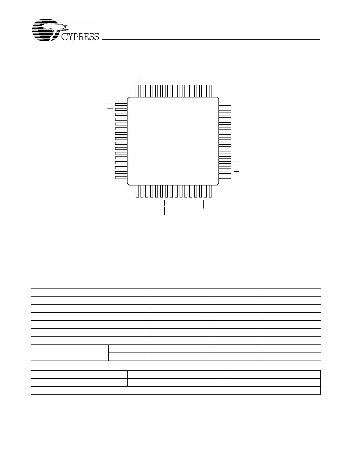
Pin Configuration
WEN
RS
D
D
D
N/C
N/C
N/C
N/C
N/C
N/C
N/C
D
D
D
D
CY7C4282V
CY7C4292V
STQFP
Top View
/LD
WCLK
XI
GND
N/C
N/C
N/C
N/C
N/C
1
2
8
7
6
5
4
3
2
3
4
5
6
7
8
9
10
11
12
13
14
15
16
17641863196220612160225923582457255626552754285329523051315032
CY7C4282V
CY7C4292V
VCCN/C
N/C
8
6
Q7Q
N/C
GND
Q
49
48
47
46
45
44
43
42
41
40
39
38
37
36
35
34
33
Q
5
Q
4
GND
Q
3
Q
2
V
CC
Q
1
Q
0
GND
N/C
FF
EF
OE
GND
FL
N/C
/RT
4282V–2
RCLK
Functional Description
(continued)
D1D
0
N/C
N/C
N/C
CC
N/C
N/C
N/C
N/C
V
PAE
PAF/XO
N/C
REN
GND
entering or exiting the Empty and Almost Empty states, the
flags are u pdated e xclus iv ely by th e RCLK. T he f lags deno ting
The CY7C4282V/92V provides four status pins: Empty, Full,
Programmab le Almost Empty, and Programmable Almost Full.
The Almost Em pty/Almost Full flags are programmable to single word granularity. The programmable flags default to Empty+7 and Full−7.
The flags are synchronous, i.e., they change state relative to
Almost Full, and Ful l st ates ar e upd ated e x clusi vel y b y WCL K.
The synchronous flag architecture guarantees that the flags
maintain their status for at least one cycle
All configurations are fabricated using an advanced 0.35µ
CMOS technology. Input ESD protection is greater than
2001V, and latch-up is prevented by the use of guard rings.
either the read cl ock (RCLK) or t he write cloc k ( WCLK). When
Selection Guide
7C4282V/92V-10 7C4282V/92V-15 7C4282V/92V-25
Maximum Frequency (MHz) 100 66.7 40
Maximum Access Time (ns) 8 10 15
Minimum Cycle Time (ns) 10 15 25
Minimum Data or Enable Set-Up (ns) 3.5 4 6
Minimum Data or Enable Hold (ns) 0 0 1
Maximum Flag Delay (ns) 8 10 15
Active Power Supply
Current (I
CC
) (mA)
Commercial 25 25 25
Industrial 30
CY7C4282V CY7C4292V
Density 64k x 9 128k x 9
Package 64-pi n 10x10 TQFP 64-pin 10x10 TQFP
2
Page 3

CY7C4282V
CY7C4292V
Pin Definitions
Signal Name Description I/O Description
D
0−8
Q
0−8
WEN Wr ite Enabl e I The only write enable when device is configured to have programmable flags. Data is
REN Read Enable I Enables the devi ce for Read operation. REN must be asserted LOW to allow a Read
WCLK Write Clock I The rising edge cloc ks data into the FIFO when WEN is LOW and the FIFO is not Full.
RCLK Read Clock I The rising edge cloc k s d ata out of the FIFO whe n R EN is LOW and the FIFO is not Empty.
EF Empty Flag O When EF is LOW, the FIFO is empty. EF is synchronized to RCLK.
FF Full Flag O When FF is LOW, the FIFO is full. FF is synchronized to WCLK.
PAE Programmable
PAF/XO Programmable
FL/RT First Load/
XI/LD Expansion In-
OE Output Enable I When OE is LOW, the FIFO’s data out pu ts driv e t he bu s t o which the y ar e co nnect-
RS Reset I Resets device t o emp ty condition. A reset is re quired before an initial read or write
Data Inputs I Data Inputs for 9-bit bus.
Data Outputs O Data Outputs for 9-bit bus.
written on a LOW-to-HIGH transition of WCLK when WEN
operation.
When LD
When LD
is asserted, WCLK writes data into the programmable flag-offset register.
is LOW, RCLK reads data out of the programmable flag-offset register.
O When PAE is LOW, the FIFO is almost empty based on the almost empty offset value pro-
Almost Empty
grammed into the FIFO. P AE
O Dual-Mode Pin:
Almost Full/
Expansion
Output
Cascaded - Connected to XI
Not Cascaded - When PAF
programmed into the FIFO. PAF
I Dual-Mode Pin:
Retransmit
Cascaded - The first device in the daisy chain will have FL
will have FL
tied to VCC. In standard mode or width expansion, FL is tied to V
on all devices.
Not Cascaded - Retran sm it function is avail able in s t a n d-alone mode by strobing
RT.
I Dual-Mode Pin:
put/Load
Cascaded - Connected to XO
Not Cascaded - LD
is used to write or read the pr ogram mab le flag of f set regist ers. LD
must be as serted LOW during reset to en able standa lone or width expansi on operation.
If programmable offset regi ster access is not requi red, LD
ed. If OE
is HIGH , the FIFO ’s outputs are in High Z (high-impedance) state.
operation after power-up.
is asserted and FF is HIGH.
is synchronized to RCLK.
of next device.
is LOW, the FIFO is almost full based on the almost full offset value
is synchronized to WCLK.
tied to VSS; all othe r device s
of previous device.
can be tied to RS directly.
SS
Maximum Ratings
(Abov e which the useful life may be impaired. For user guidelines, not tested.)
Storage Temperature .......................................−65
Ambient Temperature with
Po wer Applied.................................................... −55
Supply Voltage to Ground Potential..........−0.5V to V
DC Voltage Applied to Outputs
in High Z State..............................................−0.5V to V
DC Input Voltage.........................................−0.5V to V
Output C ur re n t in to O u tp u ts (LOW) ..... ......... ... .. ..........20 m A
°
C to +150°C
°
C to +125°C
+0.5V
CC
+0.5V
CC
+0.5V
CC
Static Discharge Voltage ......................... ............ .. ....>2001V
(per MIL-STD-883, Method 3015)
Latch-Up Current .....................................................>200 mA
Operating Range
Range
Temperature V
Commercial 0°C to +70°C 3.3V + /−300mV
Ambient
Industrial
Notes:
1. T
2. VCC Range for commercial -10 ns is 3.3V ± 150 mV.
[1]
is the “ins tant on” ca se temper at ure.
A
−40°
C to +85°C 3.3V + /−300mV
3
CC
[2]
Page 4
CY7C4282V
CY7C4292V
Electrical Characteristics
Over the Operating Range
Parameter Description Test Conditions
V
V
V
V
I
IX
I
OZL
I
OZH
I
CC1
OH
OL
IH
IL
[3]
Output HIGH Voltage VCC = Min., IOH = −1.0 mA
V
= 3.0V , IOH = −2.0 mA
CC
Output LOW Voltage VCC = Min., IOL = 4.0 mA
V
= 3.0V , IOL = 8.0 mA
CC
Input HIG H Voltage 2.0 V
Input LOW Voltage
Input Leakage Current V
Output O F F, High Z
= Max.
CC
OE > VIH, VSS < VO < V
Current
Active Power Supply
Current
[4]
I
SB
Average Standby
Current
Capacitance
[5]
Parameter Description Test Conditions Max. Unit
C
C
IN
OUT
Input Capacitance TA = 25°C, f = 1 MHz,
Output Capacitance 7 pF
7C4282V/92V
-10
7C4282V/92V
-15
7C4282V/92V
-25
UnitMin. Max. Min. Max. Min. Max.
2.4 2.4 2.4 V
0.4 0.4 0.4 V
CC
−0.5
−10
−10
CC
0.8
+10
+10
2.0 V
−0.5
−10
−10
CC
0.8
+10
+10
2.0 V
−0.5
−10
−10
CC
0.8 V
+10
+10
V
µA
µA
Com’l 25 25 25 mA
Ind 30 mA
Com’l 6 6 6 mA
Ind 6 mA
5 pF
V
= 3.3V
CC
Ω
4282V–4
[6, 7]
3.0V
GND
≤
3ns
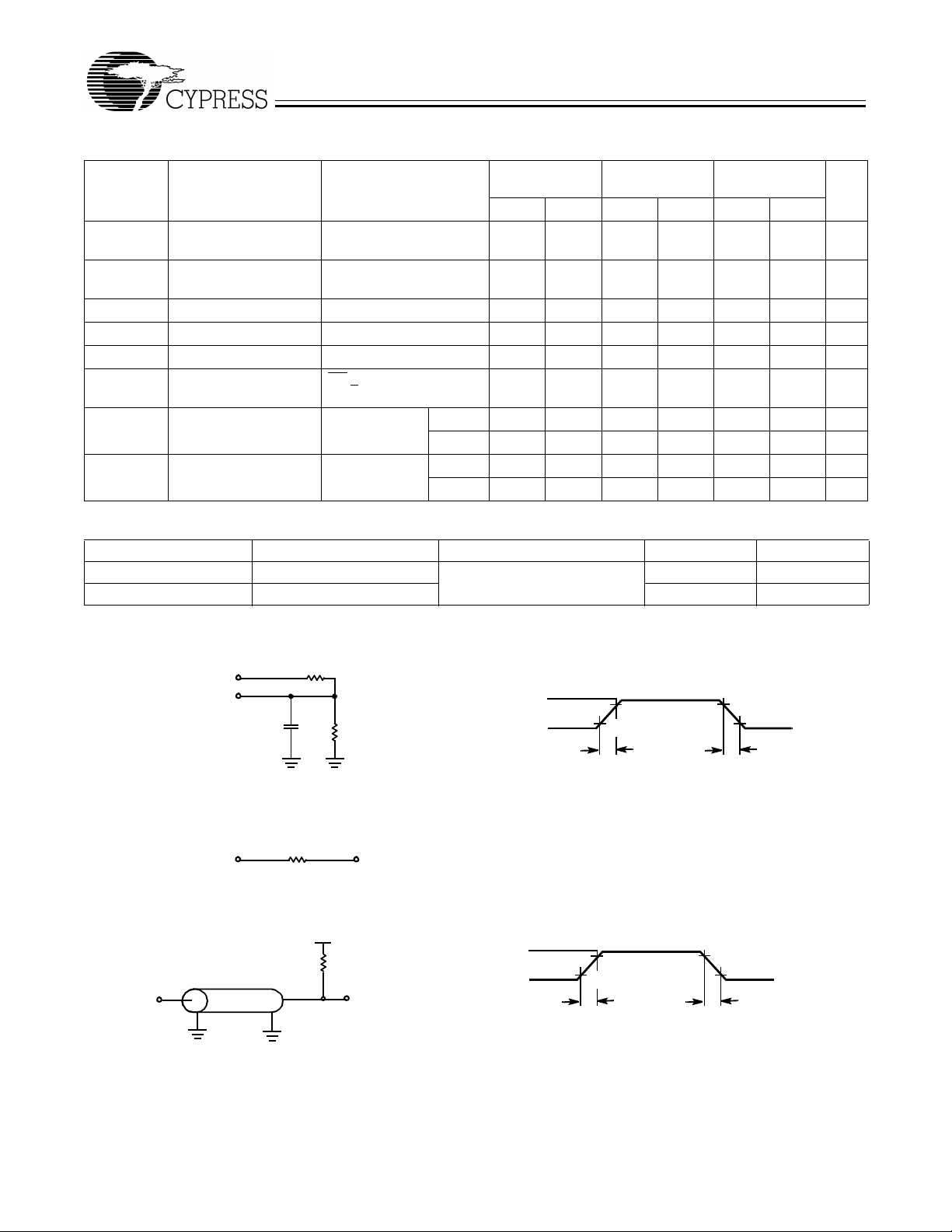
ALL INPUT PULSES
90%
10%
90%
10%
≤
3
ns
4282V–5
AC Test Loads and Waveforms (-15 , -25)
C
L
R1=330Ω
200
Ω
R2=510
3.3V
OUTPUT
INCLUDING
JIGA ND
SCOPE
Equivalent to: T HÉ VENIN EQUIVALENT
OUTPUT 2.0V
AC Test Loads and Waveforms (-10)
VCC/2
3.0V
50Ω
GND
3ns
I/O
Notes:
3. Input signals switch from 0V to 3V with a rise/fall time of less than 3 ns, clocks and clock enables switch at maximum frequency 20 MHz, while data inputs
switch a t 10 M Hz. Outputs are unloaded.
4. All inputs = V
5. Tested initially and after any design or process changes that may affect these parameters.
= 30 pF for all AC parameters except for t
6. C
L
7. C
= 5 pF f or t
L
Z0=50
Ω
− 0.2V, e xcept WCLK and RCLK (whic h a re s witching at fr equen cy = 0 MH z). Al l out puts ar e unload ed.
CC
.
OHZ
.
OHZ
≤
ALL INPUT PULSES
90%
10%
90%
10%
≤
3
ns
4282V–5
4
Page 5
CY7C4282V
CY7C4292V
Switching Characteristics
Over the Operating Range
Parameter Description
t
S
t
A
t
CLK
t
CLKH
t
CLKL
t
DS
t
DH
t
ENS
t
ENH
t
RS
t
RSS
t
RSR
t
RSF
t
PRT
t
RTR
t
OLZ
t
OE
t
OHZ
t
WFF
t
REF
t
PAF
t
PAE
t
SKEW1
t
SKEW2
Notes:
8. Pulse widths less than minimum values are not allowed.
9. Values guaranteed by design, not currently tested.
Clock Cycle Frequency 100 66.7 40 MHz
Data Access Time 2 8 2 10 2 15 ns
Clock Cycle Time 10 15 25 ns
Clock HIGH Time 4.5 6 10 ns
Clock LOW Time 4.5 6 10 ns
Data Set-Up Time 3.5 4 6 ns
Data Hold Time 0 0 1 ns
Enable Set-Up Time 3.5 4 6 ns
Enable Hold Time 0 0 1 ns
Reset Pulse Width
[8]
Reset Set-Up Time 8 10 15 ns
Reset Recovery Time 8 10 15 ns
Reset to Flag and Output Time 10 15 25 ns
Retransmit Pulse Width 60 60 60 ns
Retransmit Recovery Time 90 90 90 ns
Output Enable to Output in Low Z
Output Enable to Output Valid 3 7 3 10 3 12 ns
Output Enable to Output in High Z
Write Clock to Full Flag 8 10 15 ns
Read Clock to Empty Flag 8 10 15 ns
Clock to Prog rammable Almost-Full Flag 8 10 15 ns
Clock to Prog rammable Almost-Full Flag 8 10 15 ns
Skew Tim e between Read Clock and Write Cl ock
for Empty Fl ag and Full Flag
Skew Tim e between Read Clock and Write Cl ock
for Almost -Empty Flag and Almost-Full Fl ag
[9]
7C4282V/92V
-10
7C4282V/92V
-15
7C4282V/92V
-25
UnitMin. Max. Min. Max. Min. Max.
10 15 25 ns
0 0 0 ns
[9]
3 7 3 8 3 12 ns
5 6 10 ns
10 15 18 ns
5
Page 6

Switching Waveforms
Write Cycle Timing
WCLK
D
0–D17
WEN
FF
RCLK
t
SKEW1
t
CLKH
[10]
t
WFF
t
CLK
t
t
CLKL
DS
t
ENS
t
DH
t
ENH
t
WFF
CY7C4282V
CY7C4292V
NO OPERATION
REN
Read CycleTiming
RCLK
t
ENS
REN
EF
Q
0–Q17
OE
WCLK
WEN
t
OLZ
t
ENH
t
CLKH
t
t
REF
A
4282V–6
t
CLK
t
OE
t
t
CLKL
NO OPERATION
[11]
SKEW1
t
REF
VALID DATA
t
OHZ
Notes:
10. t
11. t
is the min imum t ime bet ween a rising RC LK edge and a r ising WCLK ed ge t o gua rantee that FF w ill go HIGH during the current clock cycle. If the time between the
SKEW1
rising edge of RCLK and the risin g edge of WCLK is less than t
is also the minimum time betw een a rising WCLK edge and a rising RCLK edge to guar antee that EF will go HIGH during the current clock cycle. It the time between
SKEW1
the rising edge of W CLK and the ris ing edge of R CLK is l ess than t
, then FF may no t c hange state unt il the ne x t WCLK risi ng edge.
SKEW1
, then EF ma y no t change st ate unti l the ne xt RCLK r ising edge.
SKEW2
6
4282V–7
Page 7

CY7C4282V
CY7C4292V
Switching Waveforms
Reset Timing
[12]
[13]
(continued)
t
RSS
LD
t
RS
RS
REN
,WEN
t
RSF
EF,PAE
t
RSF
FF,PAF
t
RSF
–
Q
Q
0
8
First Data Word Latency after Reset with Simultaneous Read and Write
t
RSR
OE=1
OE
=0
[14]
4282V–8
WCLK
t
DS
D0–D
WEN
8
t
ENS
D
(FIRSTVALIDWRITE)
0
t
SKEW1
t
[15]
FRL
RCLK
EF
REN
Q
0–Q8
t
OLZ
OE
Notes:
12. The clocks (RCLK, WCLK) can be free-running during reset.
13. For standalone or width expansion configuration only.
14. After reset, the outputs will be LOW if OE
15. When t
The Latency Timing appl ies onl y at t he Empty B ound ary (EF
16. The first word is available the cycle after EF goe s HIGH, a lwa ys .
> minimum specifi cation, t
SKEW1
= 0 and three- state if O E=1.
(maximum) = t
FRL
CLK
= LOW).
+ t
SKEW2
D
1
t
REF
. When t
t
OE
< minimum specif ication, t
SKEW1
D
2
t
A
(maximum) = eit her 2*t
FRL
D
3
[16]
t
A
D
0
+ t
CLK
SKEW1
or t
CLK
D
D
1
4282V–9
+ t
SKEW1
4
.
7
Page 8

CY7C4282V
CY7C4292V
Switching Waveforms
Empty Flag Timing
WCLK
t
DS
D0–D
WEN
RCLK
EF
REN
OE
Q
0–Q8
8
LOW
DATA WRITE 1
t
ENS
(continued)
t
ENH
[15] [15]
t
FRL
t
SKEW1
DATA IN OUTPUT REGISTER
t
REF
t
DS
DATA WRITE 2
t
ENH
t
ENS
t
FRL
t
REF
t
A
t
SKEW2
t
REF
DATA READ
Full Flag Timing
WCLK
D0–D
8
FF
WEN
RCLK
REN
OE
Q0–Q
8
NO WRITE
[10]
t
SKEW1
t
WFF
t
t
ENS
ENH
LOW
t
A
DATA IN OUTPUT REGISTER
4282V–10
NO WRITE
t
DS
t
SKEW1
[10]
DATA WRITE
DATA WRITE
t
WFF
DATA READ
t
ENS
t
WFF
t
t
ENH
A
NEXT DATA READ
4282V–11
8
Page 9

CY7C4282V
CY7C4292V
Switching Waveforms
(continued)
Programmable Almost Empty Flag Timing
t
CLKH
WCLK
t
ENS
WEN
PAE
[17]
t
SKEW2
RCLK
REN
Programmable Almost Full Flag Timing
t
CLKH
WCLK
t
ENS
WEN
t
ENH
t
CLKL
t
ENH
t
CLKL
Note
t
PAE
18
Note
20
t
ENS
N + 1 WORDS
IN FIFO
t
t
ENH
ENS
Note
19
t
PAE
4282V–12
t
PAF
PAF
FULL −(M+1)WORDS
IN FIFO
FULL −M WORDS
t
SKEW2
IN FIFO
[22]
[21]
RCLK
t
ENS
t
ENS
t
ENH
REN
Notes:
17. t
18. PAE offset= n.
19. If a read is performed on this rising edge of the read clock, there will be Empty + (n−1) words in the FIFO when PAE goes LO W
20. If a write is performed on this rising edge of the write clock, there will be Full − (m−1) words of the FIFO when PAF goes LOW.
21. 64K − m words for CY7C4282V, 128K − m words for CY4292V.
22. t
is the minimum time between a ris ing WCLK and a rising RCLK edge f or P AE to chang e state during that clock cycle. If the ti me between the edge of W CLK and the
SKEW2
rising RCLK is les s than t
is the minimum t ime betw een a risin g RCLK edge a nd a r ising WC LK edge for PAF to change during t hat cloc k cycle. If the time between the rising edge of RCLK
SKEW2
and the rising edge o f W CLK is l ess than t
, then PAE may not change state unt il the ne x t RCLK.
SKEW2
, then PAF may not change state until th e ne xt W CLK.
SKEW2
t
PAF
4282V–13
9
Page 10

CY7C4282V
CY7C4292V
Switching Waveforms
(continued)
WriteProgrammable Registers
t
CLKH
WCLK
LD
WEN
D
0–D8
Read Programmable Registers
t
CLKH
RCLK
LD
t
CLK
t
CLK
t
ENS
t
ENS
t
ENS
t
DS
t
CLKL
PAE OFFSET
LSB
t
CLKL
t
ENH
t
ENH
t
DH
PAE OFFSET
MSB
PAF OFFSET
LSB
PAF OFFSET
MSB
4282V–14
t
ENS
REN
t
A
Q
0–Q15
Retransmit Timing
[23, 24, 25]
UNKNOWN
PAE OFFSET LSB
PAE OFFSET MSB
FL/RT
t
PRT
t
RTR
REN/WEN
EF/FF
Notes:
23. Clocks are free-running in this case.
24. The flags may change state during Retransmit as a result of the offset of the read and write pointers, but flags will be valid at t
25. For the synchronous PAE and PAF flags an appropriate clock cycle is necessary after t
to update these flags.
RTR
PAF OFFSET
.
RTR
PAF OFFSET
MSB
LSB
4282V–15
4282V–16
10
Page 11

CY7C4282V
64k x 9 128kx 9
8
0
8
0
8
0
8
0
Empty Offset (LSB) Reg.
Default Value = 007h
FullOffset(LSB) Reg
Default Value = 007h
(MSB)
(MSB)
7
7
7
7
8
0
8
0
8
0
8
0
Empty Offset (LSB) Reg.
Default Value = 007h
FullOffset (LSB) Reg
Default Value = 007h
(MSB)
(MSB)
7
7
4282V–16
Default Value = 000h
Default Value = 000h
DefaultValue= 000h
Default Value = 000h
Empty Offset (LSB)
Empty Offset (MSB)
Full Offset (LSB)
Full Offset (MSB)
CY7C4292V
Architecture
The CY7C4282V/92V consists of an array of 64K to 128K
words of 9 bits each (implemented by a dual-port array of
SRAM cells), a read pointer, a write pointer, control signals
(RCLK, WCLK, REN
, WEN, RS), and flags (EF, PAE, P AF, FF).
Resetting the FIFO
Upon power-up, the FIFO must be reset with a Reset (RS)
cycle. This causes the FIFO to enter the Empty condition signified by EF
being LOW. All data out puts (Q
) go LOW t
0 − 8
RSF
after the ris ing edge of RS. In order for the FIFO to reset to its
default stat e, th e user must not read or write whi le RS
All flags ar e guar anteed to b e vali d t
During reset of t he FIFO, the stat e of t he XI
after RS is ta ken LO W .
RSF
/LD pin determines
is LOW.
if depth e xpansion oper ation is used. F or dept h e xpansi on operation, XI
/LD is tied to XO of the next device. See “Depth
Expansion Configuration” and Figure 3. For standalone or
width e xpans ion c onfigu ration, t he XI
/LD pin must be asserted
LOW during reset.
There is a 0- ns hold time requirement for the XI
tion at the RS
XI
/LD to RS di rect ly f o r appl icati ons t hat do not requir e ac cess
deassertion edge. This allows the user to tie
/LD configur a-
to the flag of fs e t re g i s te r s.
FIFO Operation
When the WEN is asserted LOW and FF is HIGH, data pres ent
on the D
of the WCLK signal. Simil arly, when the REN
and EF
on the Q
edge of RCLK while REN
before RCLK f or it to be a val id read functi on. WEN must oc cur
t
before WCLK for it to be a valid write funct ion.
ENS
An Output Enable (OE
outputs when OE is as ser ted. When OE is enabled (LOW),
data in t he output reg ister will be available to the Q
after t
output data on the FIFO that is read enabled.
pins is written into the FIFO on each rising edge
0−8
is asserted LO W
is HIGH, data in the FIFO memory will be presented
outputs. Ne w data will b e presented o n each risin g
0−8
is active. REN must set up t
) pin is provided to three-state the Q
outputs
. If devices are cascaded, the OE function will only
OE
0−8
ENS
0−8
The FIFO contains overflow circuitry to disallow additional
writes when the FIFO is full, and underflow circuitry to disallo w
additional reads when the FIFO is empty. An empty FIFO
maintains the data of the last valid read on its Q
ev en after additional reads occur.
outputs
0−8
Programming
register again. Figure 1 shows the registers sizes and default
values for the various device types.
Figure 1. Offset Register Location and Default Values
It is not nece ssary to writ e to all the offset registe rs at one time.
A subset of the offset register s can be written; then b y bringing
the LD
input HIGH, the FIFO is returned to normal read and
write operation. The next time LD
is brought LOW, a write op-
eration stores data in the next offset register in sequence.
The contents of the offset registers can be read to the data
outputs when LD
is LOW and REN is LO W . LO W-t o-H IGH tran sitions of RCLK read register contents to the data outputs.
Writes and reads should not be performed simultaneously on
the offset registers.
Programmable Flag (PAE
, P AF) Operation
Whether the flag offset registers are programmed as described in Table 1 or the default v al ues are us ed, the pr og ram-
mable Almost Empty flag (PAE
flag (PAF
) states are determined by th eir cor respondi ng offse t
) and programmab le Almost Full
registers and the difference between the read and write
pointers.
T able 1. Writing the Offset Registers
LD WEN WCLK
[26]
Selection
0 0
When LD is held LOW during Reset, this pin is the Load Enable (LD
can be us ed to access t he four 9-bit offset registers contained
in the CY7C4282V/92V for writing or reading data to these
registers.
When the device is configured for programmable flags and
both LD
of WCLK writes data from the data inputs to the empty offset
least significant bit (LSB) register. The second, third, and
fourth LOW-to-HIGH transitions of WCLK store data in the
empty offset most signi fic ant bit (MSB) reg ister, full of fset LSB
register, and full offset MSB register, respectively, when LD
and WEN are L OW . The fifth LOW -to -HIGH tra nsition of WCLK
while LD
) for flag off set pro gram ming. I n this c onfigura tion, LD
and WEN are LOW, the first LOW-to-HIGH transition
and WEN are LOW writes data to the empty LSB
0 1 No Operation
1 0 Write Into FIFO
1 1 No Operation
Note:
26. The same selection sequence applies to reading from the registers. REN
is enabled a nd a read is pe rformed on th e LO W -to -HIGH tr ansi tion of RCLK.
11
Page 12

CY7C4282V
CY7C4292V
The number formed by the empty offset least significant bit
register and empty offset most significant bit register is referred to as n and determines the operation of PAE
synchronized to the LOW-to-HIGH transition of RCLK by one
flip-flop and is LOW when the FIFO cont ains n or f ewer unrea d
words. PAE
RCLK when the FIFO cont ains ( n+1) or gr eater unread wo rds.
The number formed b y the full offset leas t significant bit register and full offset most significant bit register is referred to as
m and determines the operati on of PAF
to the LOW -t o-HIGH tr ansit ion of WCLK by one fli p-fl op and is
set LOW when the number of unread words in the FIFO is
greater than or equal to CY7C4282V (64K − m) and
CY7C4292V (128K − m). PAF
HIGH transition of WCLK when the number of avail able memory locations is great er than m.
is set HIGH by the LOW-to-HIGH transition of
. PAF is sync hronized
is set HIGH by the LOW-to-
. PAE is
Flag Operation
The CY7C4282V/92V de vic es provi de fou r flag pins to indic ate
the condition of the FIFO contents. All flags operate synchronously.
Table 2. Status Flags
Number of Words in FIFO
0 0 H H L L
[27]
1 to n
(n+1) to (65536 − (m+1)) (n+1) to (131072 − (m+1)) H H H H
(65536 − m)
65536 131072 L L H H
Notes:
27. n = Empty Offset (n=7 default value).
28. m = Full Offset (m=7 default value).
[28]
to 65535 (131072 − m)
1 to n
[27]
[28]
Full Flag
The Full Flag (FF) will go LOW when device is Full. Write operations are inhibited whenever FF
state of WEN
ly updated by each rising edge of WCLK.
Empty Flag
The Empty Flag (EF
Read operations are inhibited whenever EF
less of the state of REN
exclusively updated by each ris ing edge of RCLK.
Programmable Almost Empty/ Almost Full Flag
The CY7C4282V/92V features programmable Almost Empty
and Almost Full Flags. Each flag can be programmed (described in the Programming section) a specific distance from
the corresponding boundary flags (Empty or Full). When the
FIFO contains t he number of words o r fe wer f or which t he flags
have been prog ra mmed, the PAF
nifying that the FIFO is either Almost Full or Almost Empty . See
Table 2 for a description of programmable flags.
to 131071 H L H H
. FF is synchr onized to WCLK, i.e., it is e xclusive -
) will go LOW when the device is empty.
. EF is synchr oniz ed to RCLK, i.e . , it is
FF PAF PAE EFCY7C4282V CY7C4292V
H H L H
is LOW r ega r dl ess of th e
is LOW, regard-
or P AE will be asserted, sig-
12
Page 13

CY7C4282V
CY7C4292V
Retransmit
The retransmit feature is beneficial when transferring packets
of data. It enables the receipt of data to be acknowledged by
the receiver and retransmi tted if necessary.
The Retransmit (RT) input is activ e in the standalone and widt h
expansion modes. The retransmit feature is intended for use
when a number of writes equ al to or less t han the depth of the
FIFO hav e occurred and at least one word has been read sinc e
the last RS
pointer to the first physical location of the FIFO. WCLK and
RCLK may be free running but must be disabled during and
t
RTR
retransmit, previously accessed data is read and the read
pointer is increm ented until it i s equal to the write poi nter . Flags
are governed by the relative locations of the read and write
pointers and are updated during a ret ransmit cycle. Data writ-
FULL FLAG (FF
cycle. A HIGH pu lse on R T r esets the inte rnal rea d
after the retr ansmit pulse. With every v alid read cycle aft er
DATA IN (D)
WRITE CLOCK(WCLK)
WRITE ENABLE(WEN
LOAD(LD
PROGRAMMABLE(PAE
HALF FULL FLAG (HF
)
918
RESET
)
)
)
)
FF EF
(RS)
7C4282V
7C4292V
9
ten to the FIFO af ter ac tiv ati on of R T ar e tr ansmi tted also. The
full depth of the FIFO can be repeatedly retransmitted.
Width Expansion Configuration
Word width may be increased si m ply by connec ti ng the corre sponding inpu t contro l signal s of m ultipl e de vices. A compos ite
flag should be created for each of the end-point status flags
(EF
and FF). The partial status flags (PAE and PAF) can be
detected fr om any one device. Figure 2 demonstrates a 18-bit
word width by using t wo CY7C4282V/92V. Any word width can
be attained by adding additional CY7C4282V/92V.
When the CY7C4282V/92V is in a Width Expansion Configuration, the Read Enabl e (REN
(see Fi gure 2). In this confi gurat io n, the Loa d (LD
LOW at Rese t so t hat the p in oper at es as a con trol to l oad and
read the programmable flag offse ts.
RESET(RS)
9
7C4282V
7C4292V
FF
EF
) control input can be grounded
) pin is set to
READ CLOCK (RCLK)
READ ENABLE (REN
OUTPUT ENABLE (OE
PROGRAMMABLE (PAF
EMPTY FLAG
DATA OUT (Q)
918
)
)
)
(EF)
FIRST LOAD (FL)
EXPANSION IN (XI
Figure 2. Block Diagram of 64Kx9/12 8Kx9 Low-Voltage Deep Sync FIFO Memory Used in a Width Expansion
)
Configuration
13
FIRST LOAD (FL)
EXPANSION IN (XI
)
4282V–17
Page 14

Depth Expansion Configuration
CY7C4282V
CY7C4292V
The CY7C4282V/92V can easily be adapted to applications
requiring more than 64K/128K words of buffering. Figure 3
shows Depth Expansion using thre e CY7C4282V/92Vs. Maximum depth is limited only by signal loading. Follow these
steps:
WCLK
WEN
RS
7C4282V
7C4292V
DQ
V
CC
FL
FF EF
WCLK
WEN
RS
DATAIN (D) DATA OUT (Q)
7C4282V
7C4292V
DQ
1. The first dev ic e must be designa ted by ground ing the Fir st
Load (FL
2. All other devices must have FL
3. The Expansion Ou t (XO
the Expansion In (XI
4. EF
each individual respective flag.
XO
RCLK
REN
OE
XI
XO
RCLK
REN
OE
) control input.
in the HIGH state.
) pin of each device must be t i ed to
) pin of the ne xt device.
and FF composi te flags are created b y ORing toget her
V
CC
FL
FF
WRITECLOCK(WCLK)
WRITEENABLE
RESET
FF
Figure 3. Block Diagram of 64Kx9/128 Kx9 Low-Voltage Deep Sync FIFO Memory
(RS)
FIRST LOAD(FL)
with Programmable Flags used in Depth Expansion Configur ation
(WEN)
WCLK
WEN
7C4282V
RS
7C4292V
D
FF EF
FL
XI
XO
XI
EF
RCLK
REN
OE
Q
READCLOCK
READENABLE
OUTPUTENABLE
(RCLK)
(REN)
(OE)
EF
4282V–25
14
Page 15

CY7C4282V
CY7C4292V
Ordering Information
64K x 9 Low Voltage Deep Sync FIFO
Speed
(ns) Ordering Code
10 CY7C4282V-10ASC A64 64-Lead 10x10 Thin Quad Flatpack Commercial
15 CY7C4282V-15ASC A64 64-Lead 10x10 Thin Quad Flatpack Commercial
CY7C4282V-15ASI A64 64-Lead 10x10 Thin Quad Flatpack Industrial
25 CY7C4282V-25ASC A64 64-Lead 10x10 Thin Quad Flatpack Commercial
128K x 9 Low Voltage Deep Sync FIFO
Speed
(ns) O rdering Code
10 CY7C4292V-10ASC A64 64-Lead 10x10 Thi n Qua d Flat pack Commercial
15 CY7C4292V-15ASC A64 64-Lead 10x10 Thi n Qua d Flat pack Commercial
CY7C4292V-15ASI A64 64-Lead 10x10 Thin Qua d Flat pack Industrial
25 CY7C4292V-25ASC A64 64-Lead 10x10 Thi n Qua d Flat pack Commercial
Document #: 38-00657-B
Package Diagram
Package
Name Package Type
Package
Name Packag e Type
Operating
Range
Operating
Range
64-Pin Thin Plastic Quad Flat Pack (10 x 10 x 1.4 mm) A64
51-85051-A
© Cypress Semiconductor Corporation, 1999. The information contained herein is subject to change without notice. Cypress Semiconductor Corporation assumes no responsibility for the use
of any circuitry other than circuitry embodied in a Cypress Semiconductor product. Nor does it con vey or imply any lice nse under patent or other rights. Cypress Semicondu ctor does not authorize
its products for use as critical components in life-support systems where a malfunction or failure may reasonably be expected to result in significant injury to the user. The inclusion of Cypress
Semiconductor products in life-support systems application implies that the manufacturer assumes all risk of such use and in doing so indemnifies Cypress Semiconductor against all charges.
 Loading...