

Page 1
s
C
C
查询CY7C1379B-117AC供应商
CY7C1379B
9-Mbit (256K x 32) Flow-through SRAM
with NoBL™ Architecture
Features
• Can support up to 133-MHz bus operations with zero
wait states
— Data is transferred on every clock
• Pin compatible and functionally equivalent to ZBT™
devices
• Internally self-timed output buffer control to eliminate
the need to use
• Registered inputs for flow-through operation
• Byte Write capability
• 256K x 32 common I/O architecture
• Single 3.3V power supply
• Fast clock-to-output times
— 6.5 ns (for 133-MHz device)
— 7.0 ns (for 117-MHz device)
• Clock Enable (CEN
• Synchronous self-timed writes
• Asynchronous Output Enable
• JEDEC-standard 100 TQFP and 165 fBGA packages
• Burst Capability—linear or interleaved burst order
• Low standby power
OE
) pin to suspend operation
Functional Description
[1]
The CY7C1379B is a 3.3V, 256K x 32 Synchronous
Flow-through Burst SRAM designed specifically to support
unlimited true back-to-back Read/Write operations without the
insertion of wait states. The CY7C1379B is equipped with the
advanced No Bus Latency™ (NoBL™) logic required to
enable consecutive Read/Write operations with data being
transferred on every clock cycle. This feature dramatically
improves the throughput of data through the SRAM, especially
in systems that require frequent Write-Read transitions.
All synchronous inputs pass through input registers controlled
by the rising edge of the clock. The clock input is qualified by
the Clock Enable (CEN
) signal, which when deasserted
suspends operation and extends the previous clock cycle.
Maximum access delay from the clock rise is 6.5 ns (133-MHz
device).
Write operations are controlled by the two Byte Write Select
(BW
conducted with on-chip synchronous self-timed write circuitry.
Three synchronous Chip Enables (CE
asynchronous Output Enable (OE
) and a Write Enable (WE) input. All writes are
[A:D]
, CE2, CE3) and an
1
) provide for easy bank
selection and output three-state control. In order to avoid bus
contention, the output drivers are synchronously three-stated
during the data portion of a write sequence.
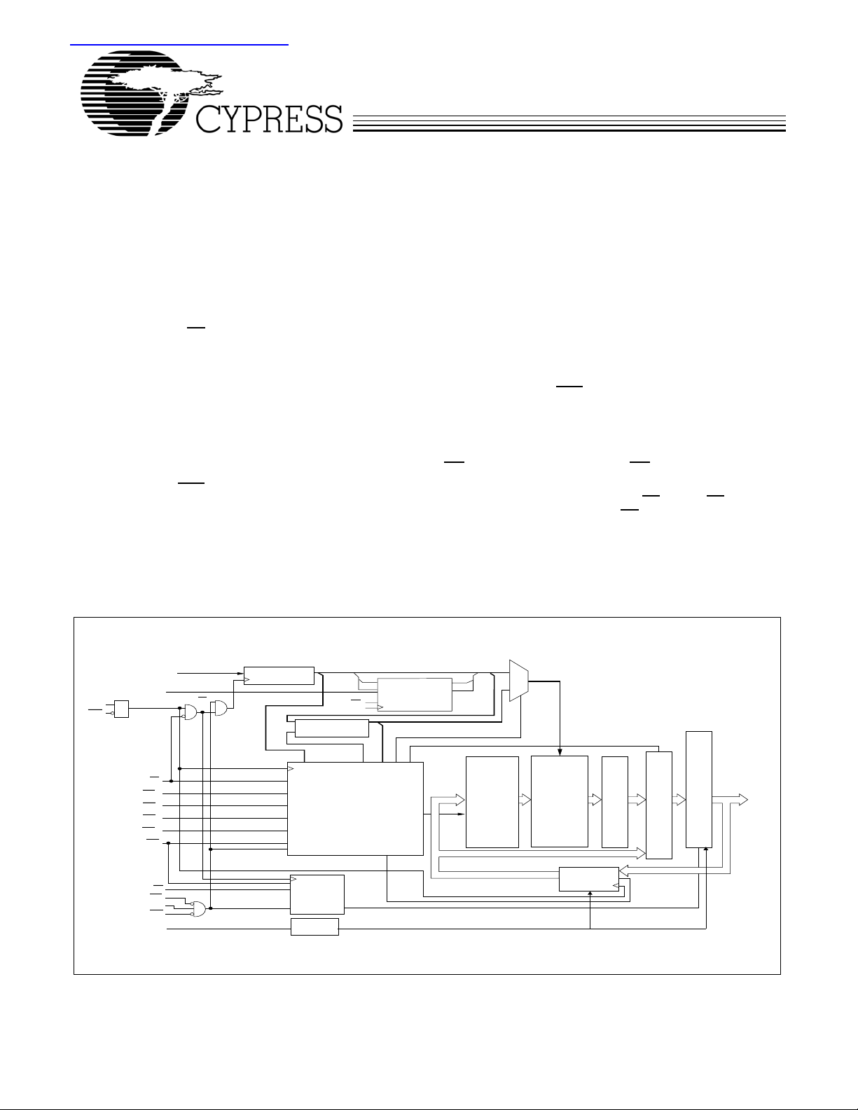
Logic Block Diagram
A0, A1, A
MODE
ADV/LD
BW
BW
BW
BW
C
A
B
C
D
WE
OE
CE1
CE2
CE3
ZZ
LK
EN
1
CE
Note:
1. For best-practices recommendations, please refer to the Cypress application note System Design Guidelines on www.cypress.com.
ADDRESS
REGISTER
ADV/LD
WRITE ADDRESS
REGISTER
WRITE REGISTRY
AND DATA COHERENCY
CONTROL LOGIC
READ LOGIC
SLEEP
Control
A1
D1
A0
D0
BURST
C
LOGIC
A1'
Q1
A0'
Q0
O
U
T
P
D
U
A
T
T
A
B
U
S
F
T
F
E
E
E
R
R
S
I
N
G
E
DQ
WRITE
DRIVERS
MEMORY
ARRAY
INPUT
REGISTER
S
E
N
S
E
A
M
P
S
E
Cypress Semiconductor Corporation • 3901 North First Street • San Jose, CA 95134 • 408-943-2600
Document #: 38-05438 Rev. *A Revised April 15, 2004
Page 2
CY7C1379B
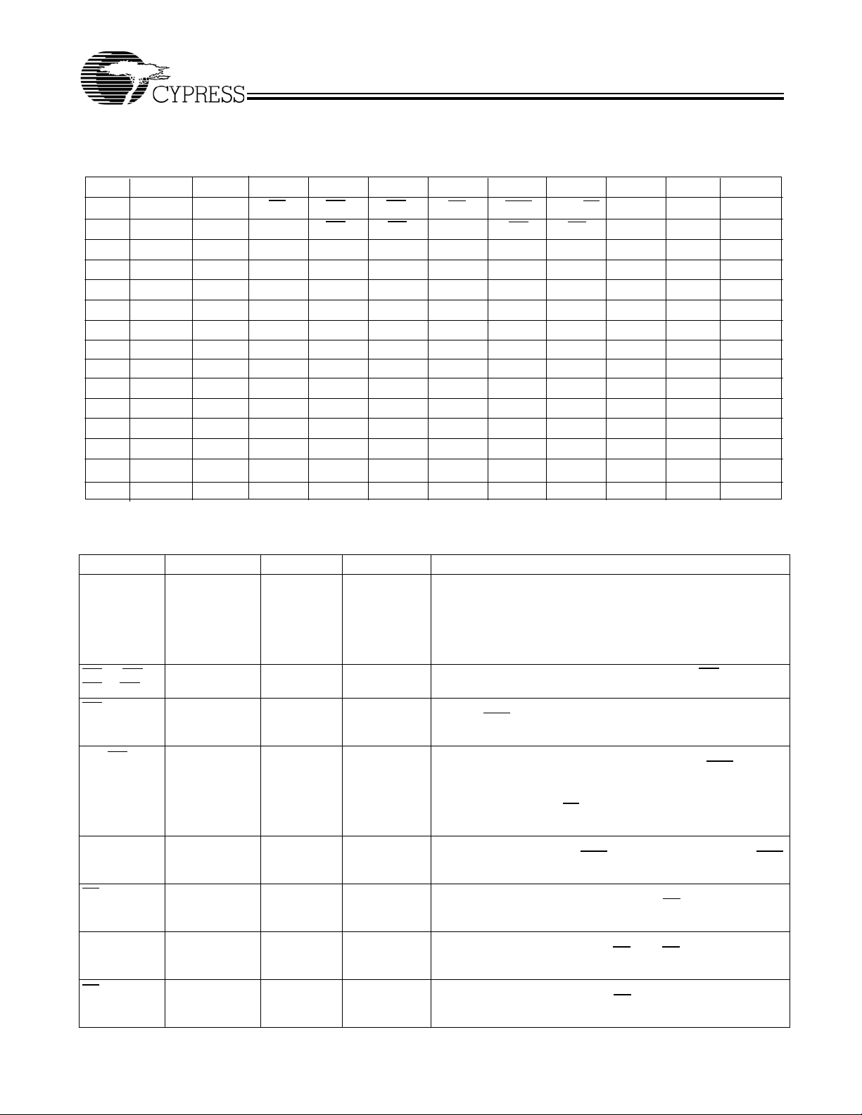
Selection Guide
133 MHz 117 MHz Unit
Maximum Access Time
Maximum Operating Current 250 220 mA
Maximum CMOS Standby Current
Shaded areas contain advance information. Please contact your local sales representative for availability of these parts.
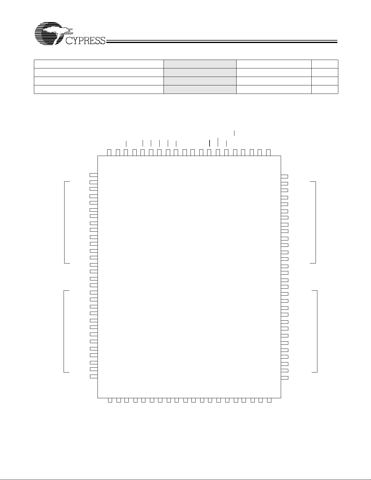
Pin Configurations
100-lead TQFP
6.5 7.0 ns
30 30 mA
BYTE C
BYTE D
1CE2
A
A
CE
100
99989796959493929190898887868584838281
NC
DQ
DQ
V
DDQ
V
DQ
DQ
DQ
DQ
V
V
DDQ
DQ
DQ
V
/DNU
SS
V
NC
V
DQ
DQ
V
DDQ
V
DQ
DQ
DQ
DQ
V
V
DDQ
DQ
DQ
NC
SS
SS
DD
SS
SS
SS
1
2
C
3
C
4
5
6
C
7
C
8
C
9
C
10
11
12
C
13
C
14
15
16
17
18
D
19
D
20
21
22
D
23
D
24
D
25
D
26
27
28
D
29
D
30
C
BWDBW
BWBBWACE3VDDV
CY7C1379B
SS
CLKWECEN
OE
ADV/LD
A
NC(18M)
A
A
80
79
78
77
76
75
74
73
72
71
70
69
68
67
66
65
64
63
62
61
60
59
58
57
56
55
54
53
52
51
NC
DQ
DQ
V
V
DQ
DQ
DQ
DQ
V
V
DQ
DQ
V
NC
V
ZZ
DQ
DQ
V
V
DQ
DQ
DQ
DQ
V
V
DQ
DQ
NC
DDQ
SS
SS
DDQ
SS
DD
DDQ
SS
SS
DDQ
B
B
B
B
BYTE B
B
B
B
B
A
A
A
A
A
A
A
A
BYTE A
31323334353637383940414243
A
A
A
A
A1
A0
MODE
NC
NC
SS
DD
V
V
44454647484950
A
A
A
NC(72M)
NC(36M)
A
A
A
A
Document #: 38-05438 Rev. *A Page 2 of 15
Page 3
Pin Configurations (continued)
234 5671
A
B
C
D
E
F
G
H
J
K
L
M
N
P
R
NC/288M
NC
NC
DQ
C
DQ
C
DQ
C
DQ
C
NC
DQ
D
DQ
D
DQ
D
DQ
D
NC
NC
MODE
A
A
NC
DQ
C
DQ
C
DQ
C
DQ
C
V
DD
DQ
D
DQ
D
DQ
D
DQ
D
NC
NC / 72M
NC / 36M
CE
CE2
V
DDQ
V
DDQ
V
DDQ
V
DDQ
V
DDQ
NC
V
DDQ
V
DDQ
V
DDQ
V
DDQ
V
DDQ
CY7C1379B
165-ball fBGA
CY7C1379B (256K x 32)
891011
BW
1
BW
V
SS
V
DD
V
DD
V
DD
V
DD
V
DD
V
DD
V
DD
V
DD
V
DD
V
SS
A
A
A
A
BW
C
D
BW
V
V
V
V
V
V
V
V
V
V
SS
SS
SS
SS
SS
SS
SS
SS
SS
SS
NC
NC
NC
CE
B
CLK
A
V
SS
V
SS
V
SS
V
SS
V
SS
V
SS
V
SS
V
SS
V
SS
V
SS
NC
A1
A0
CEN
3
WE
V
V
V
V
V
V
V
V
V
V
NC
NC
NC
SS
SS
SS
SS
SS
SS
SS
SS
SS
SS
ADV/LD
OE
V
SS
V
DD
V
DD
V
DD
V
DD
V
DD
V
DD
V
DD
V
DD
V
DD
V
SS
A
A
A
NC / 18M
V
DDQ
V
DDQ
V
DDQ
V
DDQ
V
DDQ
NC
V
DDQ
V
DDQ
V
DDQ
V
DDQ
V
DDQ
A
A
A
A
NC
NC / 144M
NC NC
DQ
DQ
DQ
DQ
DQ
B
DQ
B
DQ
B
DQ
B
NC
DQ
DQ
DQ
DQ
NC
A
DQ
A
DQ
A
DQ
A
DQ
A
NC
NC
B
B
B
B
ZZ
A
A
A
A
AA
CY7C1379B—Pin Definitions
Name TQFP fBGA I/O Description
A0, A1, A 37,36,32,33,34,
35,44,45,46,
47,48,49,50,81,
82,83,99,100
BWA, BWB,
BW
, BW
C
WE
ADV/LD
93,94,95,96 B5,A5,A4,
D
88 B7 Input-
85 A8 Input-
CLK 89 B6 Input-Clock Clock Input. Used to capture all synchronous inputs to the de-
CE
CE
CE
1
2
3
98 A3 Input-
97 B3 Input-
92 A6 Input-
R6,P6,A2,
A9,A10,B2
B10,P3,P4,
P8,P9,P10,
R3,R4,R8,
R9,R10,R11
B4
Input-
Synchronous
Input-
Synchronous
Synchronous
Synchronous
Synchronous
Synchronous
Synchronous
Address Inputs used to select one of the 256K address
locations. Sampled at the rising edge of the CLK. A
to the two-bit burst counter.
Byte Write Inputs, active LOW. Qualified with
writes to the SRAM. Sampled on the rising edge of CLK.
WE
are fed
[1:0]
to conduct
Write Enable Input, active LOW. Sampled on the rising edge
of CLK if CEN
is active LOW. This signal must be asserted LOW
to initiate a write sequence.
Advance/Load Input. Used to advance the on-chip address
counter or load a new address. When HIGH (and CEN
is asserted LOW) the internal burst counter is advanced. When LOW, a
new address can be loaded into the device for an access. After
being deselected, ADV/LD
should be driven LOW in order to load
a new address.
vice. CLK is qualified with CEN
. CLK is only recognized if CEN
is active LOW.
Chip Enable 1 Input, active LOW. Sampled on the rising edge
of CLK. Used in conjunction with CE
the device.
, and CE3 to select/deselect
2
Chip Enable 2 Input, active HIGH. Sampled on the rising edge
of CLK. Used in conjunction with CE
the device.
and CE3 to select/deselect
1
Chip Enable 3 Input, active LOW. Sampled on the rising edge
of CLK. Used in conjunction with CE
the device.
and CE2 to select/deselect
1
Document #: 38-05438 Rev. *A Page 3 of 15
Page 4
CY7C1379B—Pin Definitions(continued)
Name TQFP fBGA I/O Description
OE
CEN
86 B8 Input-
Asynchronous
87 A7 Input-
Synchronous
ZZ 64 H11 Input-
Asynchronous
DQ
s
52,53,56,57,
58,59,62,63,
68,69,72,73,
74,75,78,79,
2,3,6,7,
8,9,12,13,
18,19,22,23,
24,25,28,29
M11,L11,
K11,J11,
J10,K10,
L10,M10,
D10,E10,
F10,G10,
D11,E11,
F11,G11,
I/O-
Synchronous
D1,E1,F1,
G1,D2,E2,
F2,G2,J1,
K1,L1,M1,
J2,K2,L2
M2
Mode 31 R1 Input
Strap Pin
V
DD
15,41,65,91 D4,D8,E4,
E8,F4,F8,
Power Supply Power supply inputs to the core of the device.
G4,G8,H2,
H4,H8,J4,
J8,K4,K8,
L4,L8,M4,
M8
V
DDQ
4,11,20,27,54,
61,70,77
C3,C9,D3,
D9,E3,E9,
I/O Power
Supply
F3,F9,G3,
G9,J3,J9,
K3,K9,L3,
L9,M3,M9,
N3,N9
Output Enable, asynchronous input, active LOW. Combined
with the synchronous logic block inside the device to control the
direction of the I/O pins. When LOW, the I/O pins are allowed to
behave as outputs. When deasserted HIGH, I/O pins are
three-stated, and act as input data pins. OE
data portion of a write sequence, during the first clock when
emerging from a deselected state, when the device has been
deselected.
Clock Enable Input, active LOW. When asserted LOW the
Clock signal is recognized by the SRAM. When deasserted
HIGH the Clock signal is masked. Since deasserting CEN
not deselect the device, CEN
cycle when required.
ZZ “sleep” Input. This active HIGH input places the device in a
non-time critical “sleep” condition with data integrity preserved.
During normal operation, this pin can be connected to V
floating.
Bidirectional Data I/O Lines. As inputs, they feed into an
on-chip data register that is triggered by the rising edge of CLK.
As outputs, they deliver the data contained in the memory location specified by address during the clock rise of the Read cycle.
The direction of the pins is controlled by OE and the internal
control logic. When OE
is asserted LOW, the pins can behave
as outputs. When HIGH, DQ
tion. The outputs are automatically three-stated during the data
portion of a write sequence, during the first clock when emerging
from a deselected state, and when the device is deselected, regardless of the state of OE.
Mode Input. Selects the burst order of the device.
When tied to GND selects linear burst sequence. When tied to
VDD or left floating selects interleaved burst sequence.
Power supply for the I/O circuitry.
CY7C1379B
is masked during the
SS
does
or left
can be used to extend the previous
are placed in a three-state condi-
s
Document #: 38-05438 Rev. *A Page 4 of 15
Page 5
CY7C1379B
CY7C1379B—Pin Definitions(continued)
Name TQFP fBGA I/O Description
V
SS
NC 1,16,30,38,39,
VSS/DNU 14 - Ground/DNU This pin can be connected to Ground or should be left floating.
5,10,17,21,
26,40,55,60,
67,71,76,90,
42,43,51,66,80,
84,95,96
C4,C5,C6,
C7,C8,D5,
D6,D7,E5,
E6,E7,F5,
F6,F7,G5,
G6,G7,H5,
H6,H7,J5,
J6,J7,K5,K6,
K7,L5,L6,L7,
M5,M6,M7,
N4,N8
A1,A11,B1,
B9,B11,C1,
C2,C10,C11,
H1,H3,H9,
H10,N1,N2,
N5,N6,N7
N10,N11,P1,
P2,P5,P7,
P11,R2,R5,
R7
Ground Ground for the device.
– No Connects. Not Internally connected to the die.
18M,36M,72M, 144M and 288M are address expansion pins and
are not internally connected to the die.
Functional Overview
The CY7C1379B is a synchronous flow-through burst SRAM
designed specifically to eliminate wait states during
Write-Read transitions. All synchronous inputs pass through
input registers controlled by the rising edge of the clock. The
clock signal is qualified with the Clock Enable input signal
(CEN
). If CEN is HIGH, the clock signal is not recognized and
all internal states are maintained. All synchronous operations
are qualified with CEN. Maximum access delay from the clock
rise (t
Accesses can be initiated by asserting all three Chip Enables
(CE
Enable (CEN
the address presented to the device will be latched. The
access can either be a read or write operation, depending on
the status of the Write Enable (WE
conduct byte write operations.
Write operations are qualified by the Write Enable (WE
writes are simplified with on-chip synchronous self-timed write
circuitry.
Three synchronous Chip Enables (CE
asynchronous Output Enable (OE
All operations (Reads, Writes, and Deselects) are pipelined.
ADV/LD
deselected in order to load a new address for the next
operation.
Single Read Accesses
A read access is initiated when the following conditions are
satisfied at clock rise: (1) CEN
and CE
signal WE
LOW. The address presented to the address inputs is latched
into the Address Register and presented to the memory array
and control logic. The control logic determines that a read
) is 6.5 ns (133-MHz device).
CDV
, CE2, CE3) active at the rising edge of the clock. If Clock
1
) is active LOW and ADV/LD is asserted LOW,
). BW
can be used to
[A:D]
). All
, CE2, CE3) and an
1
) simplify depth expansion.
should be driven LOW once the device has been
is asserted LOW, (2) CE1, CE2,
are ALL asserted active, (3) the Write Enable input
3
is deasserted HIGH, and 4) ADV/LD is asserted
access is in progress and allows the requested data to
propagate to the output buffers. The data is available within 6.5
ns (133-MHz device) provided OE
is active LOW. After the first
clock of the read access, the output buffers are controlled by
OE
and the internal control logic. OE must be driven LOW in
order for the device to drive out the requested data. On the
subsequent clock, another operation (Read/Write/Deselect)
can be initiated. When the SRAM is deselected at clock rise
by one of the chip enable signals, its output will be three-stated
immediately.
Burst Read Accesses
The CY7C1379B has an on-chip burst counter that allows the
user the ability to supply a single address and conduct up to
four Reads without reasserting the address inputs. ADV/LD
must be driven LOW in order to load a new address into the
SRAM, as described in the Single Read Access section above.
The sequence of the burst counter is determined by the MODE
input signal. A LOW input on MODE selects a linear burst
mode, a HIGH selects an interleaved burst sequence. Both
burst counters use A0 and A1 in the burst sequence, and will
wrap around when incremented sufficiently. A HIGH input on
ADV/LD
the state of chip enable inputs or WE
will increment the internal burst counter regardless of
. WE is latched at the
beginning of a burst cycle. Therefore, the type of access (Read
or Write) is maintained throughout the burst sequence.
Single Write Accesses
Write access are initiated when the following conditions are
satisfied at clock rise: (1) CEN
and CE
is asserted LOW. The address presented to the address bus
are ALL asserted active, and (3) the Write signal WE
3
is asserted LOW, (2) CE1, CE2,
is loaded into the Address Register. The write signals are
latched into the Control Logic block. The data lines are
automatically three-stated regardless of the state of the OE
input signal. This allows the external logic to present the data
on DQs.
Document #: 38-05438 Rev. *A Page 5 of 15
Page 6

CY7C1379B
On the next clock rise the data presented to DQs (or a subset
for Byte Write operations, see Truth Table for details) inputs is
latched into the device and the write is complete. Additional
accesses (Read/Write/Deselect) can be initiated on this cycle.
The data written during the Write operation is controlled by
BW
capability that is described in the truth table. Asserting the
signals. The CY7C1379B provides Byte Write
[A:D]
Write Enable input (WE) with the selected Byte Write Select
input will selectively write to only the desired bytes. Bytes not
selected during a Byte Write operation will remain unaltered.
A synchronous self-timed write mechanism has been provided
to simplify the Write operations. Byte Write capability has been
included in order to greatly simplify Read/Modify/Write
sequences, which can be reduced to simple Byte Write operations.
Because the CY7C1379B is a common I/O device, data
should not be driven into the device while the outputs are
active. The Output Enable (OE
) can be deasserted HIGH
before presenting data to the DQ inputs. Doing so will
three-state the output drivers. As a safety precaution, DQs and
DQP
.are automatically three-stated during the data portion of
X
a write cycle, regardless of the state of OE
.
Burst Write Accesses
The CY7C1379B has an on-chip burst counter that allows the
user the ability to supply a single address and conduct up to
four Write operations without reasserting the address inputs.
ADV/LD
must be driven LOW in order to load the initial
address, as described in the Single Write Access section
above. When ADV/LD is driven HIGH on the subsequent clock
rise, the Chip Enables (CE
ignored and the burst counter is incremented. The correct
BW
in order to write the correct bytes of data.
inputs must be driven in each cycle of the burst write,
[A:D]
, CE2, and CE3) and WE inputs are
1
Sleep Mode
The ZZ input pin is an asynchronous input. Asserting ZZ
places the SRAM in a power conservation “sleep” mode. Two
clock cycles are required to enter into or exit from this “sleep”
mode. While in this mode, data integrity is guaranteed.
Accesses pending when entering the “sleep” mode are not
considered valid nor is the completion of the operation
guaranteed. The device must be deselected prior to entering
the “sleep” mode. CE
the duration of t
, CE2, and CE3, must remain inactive for
1
after the ZZ input returns LOW.
ZZREC
Linear Burst Address Table
(MODE = GND)
First
Address
A1, A0
00 01 10 11
01 10 11 00
10 11 00 01
11 00 01 10
Second
Address
A1, A0
Third
Address
A1, A0
Fourth
Address
A1, A0
Interleaved Burst Sequence
First
Address
A1, A0 A1, A0 A1, A0 A1, A0
00 01 10 11
01 00 11 10
10 11 00 01
11 10 01 00
Second
Address
Third
Address
Fourth
Address
ZZ Mode Electrical Characteristics
Parameter Description Test Conditions Min. Max. Unit
I
DDZZ
t
ZZS
t
ZZREC
t
ZZI
t
RZZI
Snooze mode standby current ZZ > VDD − 0.2V 35 mA
Device operation to ZZ ZZ > VDD − 0.2V 2t
ZZ recovery time ZZ < 0.2V 2t
CYC
ZZ Active to snooze current This parameter is sampled 2t
CYC
CYC
ZZ inactive to exit snooze current This parameter is sampled 0 ns
ns
ns
ns
Document #: 38-05438 Rev. *A Page 6 of 15
Page 7

CY7C1379B
Truth Table
[2, 3, 4, 5, 6, 7, 8]
Operation
ADRESS
Used CE1CE2CE
ADV/
ZZ
3
WE BWXOE CEN CLK DQ
LD
Deselect Cycle None H X X L L X X X L L->H Three-State
Deselect Cycle None X X H L L X X X L L->H Three-State
Deselect Cycle None X L X L L X X X L L->H Three-State
Continue Deselect Cycle None X X X L H X X X L L->H Three-State
READ Cycle
External L H L L L H X L L L->H Data Out (Q)
(Begin Burst)
READ Cycle
Next X X X L H X X L L L->H Data Out (Q)
(Continue Burst)
NOP/DUMMY READ
External L H L L L H X H L L->H Three-State
(Begin Burst)
DUMMY READ
Next X X X L H X X H L L->H Three-State
(Continue Burst)
WRITE Cycle
External L H L L L L L X L L->H Data In (D)
(Begin Burst)
WRITE Cycle
Next X X X L H X L X L L->H Data In (D)
(Continue Burst)
NOP/WRITE ABORT
None L H L L L L H X L L->H Three-State
(Begin Burst)
WRITE ABORT
Next X X X L H X H X L L->H Three-State
(Continue Burst)
IGNORE CLOCK
Current X X X L X X X X H L->H -
EDGE (Stall)
SNOOZE MODE None X X X H X X X X X X Three-State
Truth Table for Read/Write
Function (CY7C1379B)
[2, 3]
WE
BW
A
BW
B
BW
C
BW
Read H X X X X
Write No Bytes Written L H H H H
Write Byte A – (DQ
Write Byte B – (DQ
Write Byte C – (DQ
Write Byte D – (DQ
) L LHHH
A
)LHLHH
B
)LHHLH
C
)LHHHL
D
Write All Bytes L L L L L
Notes:
2. X =”Don't Care.” H = HIGH, L = LOW. BWx
asserted, see Truth Table for details.
3. Write is defined by BW
4. When a Write cycle is detected, all I/Os are three-stated, even during Byte Writes.
5. The DQ pins are controlled by the current cycle and the OE
= H, inserts wait states.
6. CEN
7. Device will power-up deselected and the I/Os in a three-state condition, regardless of OE
is asynchronous and is not sampled with the clock rise. It is masked internally during write cycles. During a read cycle DQs = Three-state when OE is inactive
8. OE
or when the device is deselected, and DQs = data when OE
, and WE. See Truth Table for Read/Write.
X
= 0 signifies at least one Byte Write Select is active, BWx = Valid signifies that the desired byte write selects are
signal. OE is asynchronous and is not sampled with the clock.
.
is active.
D
Document #: 38-05438 Rev. *A Page 7 of 15
Page 8

CY7C1379B
Maximum Ratings
Static Discharge Voltage.......................................... > 2001V
(per MIL-STD-883, Method 3015)
(Above which the useful life may be impaired. For user guidelines, not tested.)
Storage Temperature .................................–65°C to +150°C
Ambient Temperature with
Power Applied.............................................–55°C to +125°C
Supply Voltage on V
Relative to GND........ –0.5V to +4.6V
DD
DC Voltage Applied to Outputs
in High-Z State .................................... –0.5V to V
DC Input Voltage....................................–0.5V to V
DDQ
DD
+ 0.5V
+ 0.5V
Latch-up Current.................................................... > 200 mA
Operating Range
Ambient
Range
Com’l 0°C to +70°C 3.3V -
Temperature (T
) V
A
DD
5%/+10%
V
DDQ
3.3V - 5% to
V
DD
Current into Outputs (LOW) .........................................20 mA
Electrical Characteristics
Over the Operating Range
[9,10]
Parameter Description Test Conditions Min. Max. Unit
V
DD
V
DDQ
V
OH
V
OL
V
IH
V
IL
I
X
I
OZ
I
OS
I
DD
I
SB1
I
SB2
I
SB3
I
SB4
Notes:
9. Overshoot: V
10. T
Power-up
Power Supply Voltage 3.135 3.6 V
I/O Supply Voltage 3.135 V
Output HIGH Voltage V
Output LOW Voltage V
Input HIGH Voltage V
Input LOW Voltage
[9]
Input Load Current
(except ZZ and MODE)
Input Current of MODE Input = V
Input Current of ZZ Input = V
= 3.3V, VDD = Min., I
DDQ
= 3.3V, VDD = Min., I
DDQ
= 3.3V 2.0 VDD + 0.3V V
DDQ
V
= 3.3V –0.3 0.8 V
DDQ
GND ≤ VI ≤ V
Input = V
Input = V
DDQ
SS
DDQ
SS
DDQ
= –4.0 mA 2.4 V
OH
= 8.0 mA 0.4 V
OL
−5 5 µA
–30 µA
–5 µA
DD
5 µA
30 µA
Output Leakage Current GND ≤ VI ≤ VDD, Output Disabled –5 5 µA
Output Short Circuit
Current
V
Operating Supply
DD
Current
Automatic CE Power-down
Current—TTL Inputs
Automatic CE Power-down
Current—CMOS Inputs
Automatic CE Power-down
Current—CMOS Inputs
Automatic CE Power-down
Current—TTL Inputs
(AC) < V
IH
: Assumes a linear ramp from 0V to V
+1.5V (Pulse width less than t
DD
V
= Max., V
DD
V
= Max., I
DD
f = f
V
V
inputs switching
V
V
f = 0, inputs static
V
V
f = f
V
V
f = 0, inputs static
(min.) within 200 ms. During this time VIH < VDD and V
DD
= 1/t
MAX
= Max, Device Deselected,
DD
≥ VIH or VIN ≤ VIL, f = f
IN
= Max, Device Deselected,
DD
≥ VDD – 0.3V or VIN ≤ 0.3V,
IN
= Max, Device Deselected,
DD
≥ V
IN
DDQ
, inputs switching
MAX
= Max, Device Deselected,
DD
≥ V
IN
– 0.3V or VIN ≤ 0.3V,
DD
/2), undershoot: VIL(AC)> –2V (Pulse width less than t
CYC
= GND –300 µA
OUT
OUT
CYC
= 0 mA,
7.5-ns cycle, 133 MHz 250 mA
8.5-ns cycle, 117 MHz 220 mA
All speeds 40 mA
,
MAX
All speeds 30 mA
All speeds 40 mA
– 0.3V or VIN ≤ 0.3V,
All speeds 40 mA
DDQ
< V
DD
CYC
.
/2).
V
Document #: 38-05438 Rev. *A Page 8 of 15
Page 9

CY7C1379B
Thermal Resistance
[11]
Parameters Description Test Conditions TQFP Package fBGA Package Unit
Θ
JA
Θ
JC
Capacitance
Thermal Resistance
(Junction to Ambient)
Thermal Resistance
(Junction to Case)
[11]
Test conditions follow standard test
methods and procedures for measuring thermal impedance, per
EIA/JESD51
25 27 °C/W
96°C/W
Parameter Description Test Conditions TQFP Package fBGA Package Unit
C
IN
C
CLOCK
C
I/O
Input Capacitance TA = 25°C, f = 1 MHz,
V
= 3.3V
Clock Input Capacitance 57pF
I/O Capacitance 5 7 pF
V
DD
DDQ
=3.3V
57pF
AC Test Loads and Waveforms
3.3V I/O Test Load
OUTPUT
Z
= 50Ω
0
R
L
3.3V
OUTPUT
= 50Ω
5pF
VL= 1.5V
INCLUDING
(a)
Note:
11.Tested initially and after any design or process changes that may affect these parameters.
JIG AND
SCOPE
R = 317Ω
(b)
R = 351Ω
V
GND
DD
≤ 1 ns
ALL INPUT PULSES
10%
90%
90%
(c)
10%
≤ 1 ns
Document #: 38-05438 Rev. *A Page 9 of 15
Page 10

CY7C1379B
Switching Characteristics Over the Operating Range
[12, 13, 14, 15, 16, 17]
133 MHz 117 MHz
Parameter Description
t
POWER
VDD(Typical) to the First Access
[14]
1 1 ms
Clock
t
CYC
t
CH
t
CL
Clock Cycle Time 7.5 8.5 ns
Clock HIGH 3.0 3.2 ns
Clock LOW 3.0 3.2 ns
Output Times
t
CDV
t
DOH
t
CLZ
t
CHZ
t
OEV
t
OELZ
t
OEHZ
Data Output Valid after CLK Rise 6.5 7.0 ns
Data Output Hold after CLK Rise 2.0 2.0 ns
Clock to Low-Z
Clock to High-Z
[15, 16, 17]
[15, 16, 17]
0 0 ns
3.5 3.5 ns
OE LOW to Output Valid 3.5 3.5 ns
OE LOW to Output Low-Z
OE HIGH to Output High-Z
[15, 16, 17]
[15, 16, 17]
0 0 ns
3.5 3.5 ns
Set-up Times
t
AS
t
ALS
t
WES
t
CENS
t
DS
t
CES
Address Set-up before CLK Rise 1.5 1.5 ns
ADV/LD Set-up before CLK Rise 1.5 1.5 ns
WE, BW
Set-up before CLK Rise 1.5 1.5 ns
[A:D]
CEN Set-up before CLK Rise 1.5 1.5 ns
Data Input Set-up before CLK Rise 1.5 1.5 ns
Chip Enable Set-up before CLK Rise 1.5 1.5 ns
Hold Times
t
AH
t
ALH
t
WEH
t
CENH
t
DH
t
CEH
Notes:
12. Timing reference level is 1.5V when V
13. Test conditions shown in (a) of AC Test Loads, unless otherwise noted.
14. This part has a voltage regulator internally; t
can be initiated.
, t
15. t
CHZ
CLZ,tOELZ
16. At any given voltage and temperature, t
data bus. These specifications do not imply a bus contention condition, but reflect parameters guaranteed over worst case user conditions. Device is designed
to achieve High-Z prior to Low-Z under the same system conditions
17. This parameter is sampled and not 100% tested.
Address Hold after CLK Rise 0.5 0.5 ns
ADV/LD Hold after CLK Rise 0.5 0.5 ns
WE, BWX Hold after CLK Rise 0.5 0.5 ns
CEN Hold after CLK Rise 0.5 0.5 ns
Data Input Hold after CLK Rise 0.5 0.5 ns
Chip Enable Hold after CLK Rise 0.5 0.5 ns
=3.3V
DDQ
, and t
is the time that the power needs to be supplied above V
POWER
are specified with AC test conditions shown in part (b) of AC Test Loads. Transition is measured ± 200 mV from steady-state voltage.
OEHZ
OEHZ
is less than t
OELZ
and t
is less than t
CHZ
to eliminate bus contention between SRAMs when sharing the same
CLZ
(minimum) initially, before a read or write operation
DD
UnitMin. Max. Min. Max.
Document #: 38-05438 Rev. *A Page 10 of 15
Page 11

Switching Waveforms
123456789
10
C
Read/Write Waveforms
CLK
t
CENS
CEN
t
CES
CE
ADV/LD
WE
BW
[A:D]
[18, 19, 20]
t
CENH
t
CEH
CY7C1379B
t
CYC
t
t
CL
CH
ADDRESS
DQ
A1 A2
t
t
AH
AS
D(A1) D(A2) Q(A4)Q(A3)
t
t
DH
DS
A3
t
CDV
t
CLZ
D(A2+1)
OE
OMMAND
Notes:
For this waveform ZZ is tied LOW.
18.
19. When CE
20. Order of the Burst sequence is determined by the status of the MODE (0 = Linear, 1 = Interleaved). Burst operations are optional.
is LOW, CE1 is LOW, CE2 is HIGH and CE3 is LOW. When CE is HIGH, CE1 is HIGH or CE2 is LOW or CE3 is HIGH.
WRITE
D(A1)
WRITE
D(A2)
BURST
WRITE
D(A2+1)
READ
Q(A3)
DON’T CARE UNDEFINED
A4
t
READ
Q(A4)
DOH
t
OEHZ
BURST
READ
Q(A4+1)
A5 A6 A7
t
OEV
t
OELZ
t
CHZ
Q(A4+1)
t
DOH
WRITE
D(A5)
D(A5)
READ
Q(A6)
WRITE
D(A7)
D(A7)Q(A6)
DESELECT
Document #: 38-05438 Rev. *A Page 11 of 15
Page 12

Switching Waveforms (continued)
45678910
123
C
A
NOP, STALL and Deselect Cycles
CLK
CEN
CE
ADV/LD
WE
BW
[A:D]
[18, 19, 21]
CY7C1379B
ADDRESS
DQ
OMMAND
D(A1)
ZZ Mode Timing
CLK
ZZ
I
SUPPLY
LL INPUTS
(except ZZ)
Outputs (Q)
A1 A2
READ
Q(A2)
[22, 23]
A3 A4
Q(A2)D(A1) Q(A3)
STALL NOP READ
READ
Q(A3)
WRITE
D(A4)
STALLWRITE
D(A4)
DON’T CARE UNDEFINED
t
ZZ
t
ZZI
I
DDZZ
High-Z
A5
t
DOH
Q(A5)
DESELECT CONTINUE
t
RZZI
DESELECT or READ Only
Q(A5)
t
CHZ
t
ZZREC
DESELECT
DON’T CARE
Notes:
21. The IGNORE CLOCK EDGE or STALL cycle (Clock 3) illustrated CEN
22. Device must be deselected when entering ZZ mode. See truth table for all possible signal conditions to deselect the device.
23. I/Os are in High-Z when exiting ZZ sleep mode.
being used to create a pause. A write is not performed during this cycle.
Document #: 38-05438 Rev. *A Page 12 of 15
Page 13

CY7C1379B
Ordering Information
Speed
(MHz) Ordering Code
117 CY7C1379B-117AC A101 100-Lead 14 x 20 x 1.4 mm Thin Quad Flat Pack Commercial
CY7C1379B-117BZC BB165A 165-ball Fine-Pitch Ball Grid Array (13x15x1.2mm)
Please contain your local sales representative for availability of 133-MHz speed grade option
Package Diagrams
100-lead Thin Plastic Quad Flatpack (14 x 20 x 1.4 mm) A101
Package
Name Package Type
Operating
Range
51-85050-A
Document #: 38-05438 Rev. *A Page 13 of 15
Page 14

Package Diagrams (continued)
CY7C1379B
165-Ball FBGA (13 x 15 x 1.2 mm) BB165A
51-85122-*C
NoBL and No Bus Latency are trademarks of Cypress Semiconductor Corporation. ZBT is a trademark of Integrated Device
Technology. All product and company names mentioned in this document are the trademarks of their respective holders.
Document #: 38-05438 Rev. *A Page 14 of 15
© Cypress Semiconductor Corporation, 2004. The information contained herein is subject to change without notice. Cypress Semiconductor Corporation assumes no responsibility for the use
of any circuitry other than circuitry embodied in a Cypress Semiconductor product. Nor does it convey or imply any license under patent or other rights. Cypress Semiconductor d oes not authorize
its products for use as critical components in life-support systems where a malfunction or failure may reasonably be expected to result in significant injury to the user. The inclusion of Cypress
Semiconductor products in life-support systems application implies that the manufacturer assumes all risk of such use and in doing so indemnifies Cypress Semiconductor against all charges.
Page 15

CY7C1379B
Document History Page
Document Title: CY7C1379B 9-Mbit (256K x 32) Flow-through SRAM with NoBL™ Architecture
Document #: 38-05438 Rev. *A
REV. ECN NO. Issue Date
** 201060 See ECN NJY New Data Sheet
*A 225181 See ECN VBL Update Ordering Info section: shade part numbers, add explanation
Orig. of
Change Description of Change
Document #: 38-05438 Rev. *A Page 15 of 15
 Loading...