

Datasheet CY7C1335L-75AC, CY7C1335L-66AC, CY7C1335L-60AC, CY7C1335L-100AC, CY7C1335-75AC Datasheet (Cypress Semiconductor)
...Page 1

32K x 32 Synchronous-Pipelined Cache RAM
CY7C1335
Cypress Semiconductor Corporation
• 3901 North First Street • San Jose • CA 95134 • 408-943-2600
July 30, 1999
aven’t
re
2CY7C 1329
Features
• Supports 100-MHz bus for Pentium and PowerPC™
operations with zero wait states
• Fully registered inputs and outputs for pipelined
operation
• 32K by 32 common I/O architecture
• Single 3.3V power supply
• Fast clock-to-output times
—4.2 ns (for 133-MHz device)
—5.5 ns (for 100-MHz device)
—7.0 ns (for 75-MHz devi ce
• User-selectable burst counter supporting Intel
Pentium interleaved or linear burst sequences
• Separate processor and controller address strobes
• Synchronous self-timed writes
• Asynchronous output enable
• JEDEC-standard 100 TQFP pinout
• “ZZ” Sleep Mode option and Stop Clock option
Functional Description
The CY7C1335 is a 3.3V, 32K by 32 synchronous-pipelined
cache SRAM designed to support zero wait state secondary
cache with minimal glue logic.
All synchronous input s pass through i nput regist er s controll ed
by the rising edge of the clock. All data outputs pass through
output registers cont rolled by the rising edge of the clock. Maximum access delay from the clock rise is 4.2 ns (133-MHz
device).
The CY7C1335 supports either the interleaved burst sequence used by the Intel Pent ium processor or a linear burst
sequence used b y processors such as the P ower PC. The burs t
sequence is selected through the MODE pin. Accesses can
be initiated by asserting either the Processor Address Strobe
(ADSP
) or the Controller Addr ess Strobe (ADSC) at clock ri se.
Address advancement through the burst sequence is controlled by the ADV
input. A 2-bit on-chip wraparound burst
counter captures the first address in a burst sequence and
automatically increments the address for the rest of the burst
access.
Byte write operations are qualified with the four Byte Write
Select (BW
[3:0]
) inputs. A Global Write Enabl e (G W) ov er rides
all byte write inputs and writes data to all four bytes. All writes
are conducted with on-chip synchronous self-timed write circuitry.
Three synchronous Chip Selects (CE
1
, CE2, CE3) and an
asynchronous Output Enable (OE
) provide for easy bank selection and output thr ee-state con trol. In order to pro vide proper data during dep th expansion, OE
is masked duri ng the first
clock of a read c ycle when emerging from a deselected state .
Intel and Pentium are registered trademarks of Intel Corporation.
PowerPC is a trademark of IBM Corporation.
CLK
ADV
ADSC
A
[14:0]
GW
BWE
BW
3
BW
2
BW
1
BW
0
CE
1
CE
3
CE
2
OE
ZZ
BURST
COUNTER
DQ[31:24]
BYTEWRITE
REGISTERS
ADDRESS
REGISTER
D
Q
OUTPUT
REGISTERS
INPUT
REGISTERS
32KX32
MEMORY
ARRAY
CLK
CLK
Q
0
Q
1
Q
D
CE
CE
CLR
SLEEP
CONTROL
DQ[23:16]
BYTEWRITE
REGISTERS
D
Q
DQ
DQ[15:8]
BYTEWRITE
REGISTERS
DQ[7:0]
BYTEWRITE
REGISTERS
D Q
ENABLE
REGISTER
D
Q
CE
CLK
ENABLE DELAY
REGISTER
D Q
CLK
32 32
15
13
13
15
(A
[1;0]
)
2
MODE
ADSP
Logic Block Diagram
DQ
[31:0]
Page 2

CY7C1335
2
Pin Configuration
A5A4A3A2A1A
0
NC
NC
V
SS
V
DD
NC
NC
A
10A11A12A13A14
NC
NC
NC
DQ
15
DQ
14
V
DDQ
V
SSQ
DQ
13
DQ
12
DQ
11
DQ
10
V
SSQ
V
DDQ
DQ
9
DQ
8
V
SS
NC
V
DD
ZZ
DQ
7
DQ
6
V
DDQ
V
SSQ
DQ
5
DQ
4
DQ
3
DQ
2
V
SSQ
V
DDQ
DQ
1
DQ
0
NC
NC
DQ
16
DQ
17
V
DDQ
V
SSQ
DQ
18
DQ
19
DQ
20
DQ
21
V
SSQ
V
DDQ
DQ
22
DQ
23
NC
V
DD
NC
V
SS
DQ
24
DQ
25
V
DDQ
V
SSQ
DQ
26
DQ
27
DQ
28
DQ
29
V
SSQ
V
DDQ
DQ
30
DQ
31
NC
A6A7CE1CE2BW3BW2BW1BW0CE3VDDVSSCLKGWBWEOEADSC
ADSP
ADV
A8A
9
1
2
3
4
5
6
7
8
9
10
11
12
13
14
15
16
17
18
19
20
21
22
23
24
25
26
27
28
29
30
31323334353637383940414243444546474849
50
80
79
78
77
76
75
74
73
72
71
70
69
68
67
66
65
64
63
62
61
60
59
58
57
56
55
54
53
52
51
100999897969594939291908988878685848382
81
MODE
BYTE0
BYTE1
BYTE3
BYTE2
100-Pin TQFP
CY7C1335
Selectio n Guide
7C1335-133 7C1335-100 7C1335-75
Maximum Access Time (ns) 4.2 5.5 7.0
Maximum Operating Curr ent (mA) Commercial 325 310 260
Maximum CMOS Standby Current (mA) Commercial 5 5 5
Page 3

CY7C1335
3
Pin Definitions
Pin Number Name I/O Description
48–44, 81,
82, 99, 100,
32–37
A
[14:0]
Input-
Synchronous
Address Inputs used to select one of the 64K address locations. Sampled at th e
rising edge of the CLK if ADSP
or ADSC is active LOW, and CE1, CE2, and CE
3
are sampled active. A
[1:0]
feed the 2-bi t counter.
96–93 BW
[3:0]
Input-
Synchronous
Byte Write Select Inputs, active LOW. Qualified with BWE to conduct byte writes
to the SRAM. Sampled on the rising edge of CLK.
88 GW Input-
Synchronous
Global Write Enable I nput, acti ve LOW. When asserted LOW on the rising edge of
CLK, a global write is conducted (ALL bytes are writte n, regardless of the values
on BW
[3:0]
and BWE).
87 BWE Input-
Synchronous
Byte Write Enable Input , active LOW. Sampled on the rising edge of CLK. This
signal must be asserted LO W to conduct a byte write.
89 CLK Input-Clock Clock Input. Used to capture all synchronous inputs to the device. Also used to
increment t he burst counter when ADV
is asserted LOW, during a burst operation.
98 CE
1
Input-
Synchronous
Chip Enable 1 Input, active LOW. Sampled on the rising edge of CLK. Used in
conjunction with CE
2
and CE3 to select/deselect the device. ADSP is ignored if
CE
1
is HIGH.
97 CE
2
Input-
Synchronous
Chip Enable 2 Input, active HIGH. Sampled on the rising edge of CLK. Used in
conjunction with CE
1
and CE3 to select/deselect the device.
92 CE
3
Input-
Synchronous
Chip Enable 3 Input, active LOW. Sampled on the rising edge of CLK. Used in
conjunction with CE
1
and CE2 to select/deselect the device.
86 OE Input-
Asynchronous
Output Enable, asynchronous input, active LOW. Controls the direction of the I/O
pins. When LO W , the I/O pins behave as outputs. When deasserted HIGH, I/O pins
are three-stat ed, and a ct a s input data pi ns . OE
is masked duri ng the f irst cloc k of
a read cycle when emergin g from a deselected state.
83 ADV Input-
Synchronous
Advance Input signal , samp led on the risi ng edge of CLK. When asserted, it automatically increments the address in a burst cycle.
84 ADSP Input-
Synchronous
Address Strobe from Proce ssor , sampled on t he rising edge of CLK. When asserted LOW , A
[14:0]
is captur ed in t he ad dress r egist ers. A
[1:0]
are also loa ded int o the
burst c ounter. When ADSP
and ADSC are both ass erted, only ADSP is recogniz ed.
ASDP
is ignored when CE1 is deasserted HIGH.
85 ADSC Input-
Synchronous
Address Strobe from Cont roll er , sa mpled on the ri sing e dge of CLK. When as serted LOW , A
[14:0]
is captur ed in t he ad dress r egist ers. A
[1:0]
are also loa ded int o the
burst counter. When ADSP
and ADSC are both asserted, only ADSP is r ecognize d.
64 ZZ Input-
Asynchronous
ZZ “sleep” Input. This active HIGH input places the de vice in a non-time-crit ical
“sleep” condition wi th data integrity preserved.
29, 28,
25–22,19,
18,13,12,
9–6, 3, 2, 79,
78, 75–72,
69, 68, 63, 62
59–56, 53, 52
DQ
[31:0]
I/O-
Synchronous
Bidirectional Data I/O line s. As inputs, they feed into an on-chip data register that
is triggered by t he rising edge of CLK. As outputs , the y deliver the data contained
in the memory location specif ied by A
[14:0]
during the previous clock rise of the
read cycle. The dir ection of the pins is controlled by OE
. When OE is asserted
LOW , the pins behav e as outputs. When HIG H, DQ
[31:0]
are placed in a three-state
condition.
15, 41, 65, 91 V
DD
Power Supply Po wer su ppl y inpu ts to t he core of t he de vice . Shou ld be conn ect ed to 3.3V po wer
supply.
17, 40, 67, 90 V
SS
Ground Ground for the core of the device. Should be connected to ground of the system.
4, 11, 20, 27,
54, 61, 70, 77
V
DDQ
I/O Power
Supply
Po wer supply for the I/O ci rcuitry . Should be connected to a 3.3 V power supply.
5, 10, 21, 26,
55, 60, 71, 76
V
SSQ
I/O Ground Ground for the I/O circuitry. Should be connected to ground of the syst em .
31 MODE Input-
Static
Selects burs t order. When ti ed to GND selects linear burst sequence. When tied
to V
DDQ
or left floating selec ts interleav ed burst sequence. Thi s is a strap pin and
should remain sta tic during device ope ration.
1, 14, 16, 30,
38, 39, 42, 43,
49, 50, 51, 66,
80
NC No Connects.
Page 4

CY7C1335
4
Introduction
Functional Overview
All synchrono us inputs pass throu gh inp ut registe rs con trol led
by the rising edge of the clock. All data outputs pass through
output regi sters co ntrolle d by the rising ed ge of the clock. Maximum access del ay from the clo ck rise (t
CO
) is 4.2 ns (133-MHz
device).
The CY7C1335 sup ports secondary cache in systems utilizin g
either a linear or interleaved burst sequence. The interleaved
burst order supports Pen ti um and i486 processors. The linear
burst sequence is suited for processors that utilize a linear
burst sequence. The burst order is user selectable, and i s determined by sampling the MODE input. Accesses can be initiated with either the Processor Address Strobe (ADSP
) or the
Controller Address Strobe (ADSC
). Address advancement
through the burst sequence is controlled by the ADV
input. A
two-bit on -chip wraparou nd burs t counter captu res the fi rst address in a burst sequence and automatically increments the
addr e s s for the rest of the bu rst acce ss.
Byte write operations are qualified with the Byt e Writ e Enable
(BWE
) and Byte Write Select (BW
[3:0]
) inputs. A Global Write
Enable (GW
) overrides all byte write inpu ts and writes data to
all four bytes. All writes are simplified with on-chip synchronous self-timed wri te circuitry.
Three synchronous Chip Selects (CE
1
, CE2, CE3) and an
asynchronous Output Enable (OE
) provide for easy bank se-
lection and output three-state control. ADSP
is ignored if CE
1
is HIGH.
Single Read Accesses
This access is initiated when the following conditions are satisfied at clock rise: (1) ADSP
or ADSC is asserted LOW, (2)
CE
1
, CE2, CE3 are all ass erted active , and (3) the write sign als
(GW
, BWE) are all deasserted HIGH. ADSP is ignored if CE
1
is HIGH. The address pre sented to the address i nputs (A
[14:0]
)
is stored into t he address adv anc ement logi c and the Addr ess
Register while being presented to the memory core. The corresponding data is allowed to propagate to the input of the
Output Regist ers. At the rising edge of the next clock the data
is allowed to propagate through the output register and onto
the data bus within 4.2 ns (133-MHz device) if OE
is active
LOW. The only ex ceptio n occurs when the SRAM is emerg ing
from a deselected state to a selected state, its outputs are
always three-stated during the first cycle of the access. After
the first cycle of the access, the outputs are controlled by the
OE
signal. Consecutive single read cycles are supported.
Once the SRAM is deselected at clock rise by the chip select
and either ADSP
or ADSC signals, its output will three-state
immediately.
Single Write Accesses In it iated by ADSP
This access is initiated when both of the following conditions
are satisfied at clock rise: (1) ADSP
is asserted LOW, and (2)
CE
1
, CE2, CE3 are all a sserted act iv e. Th e add res s prese nted
to A
[14:0]
is loaded into the address register and the address
advance ment logic while being delivered to the RAM core. The
write signals (GW
, BWE, and BW
[3:0]
) and ADV inputs are ig-
nored during this first cycle .
ADSP
-triggered write accesses require two clock cycles to
comple te. If GW
is asserted LOW on the seco nd cloc k rise, the
data presented to the DQ
[31:0]
inputs is written into the corre-
sponding address location in the RAM core. If GW
is HIGH,
then the write oper ation is cont rolled by BWE
and BW
[3:0]
signals. The CY7C1335 provides byte write capability that is described in the Write Cycle Description Table. Asserting the
Byte Write Enable input (BWE
) with the selected Byte Write
(BW
[3:0]
) input will selectively write to only the desired bytes.
Bytes not selected during a byte write operation will remain
unaltered. A synchronous self-timed write mechanism has
been provided to sim plify the write operations .
Because the CY7C1335 is a common I/O device, the Output
Enable (OE
) must be deasse rted HIGH bef ore pre senting data
to the DQ
[31:0]
inputs. Doing so will three-sta te the out put driv -
ers. As a safety precaution, DQ
[31:0]
are automatically
three-stated whenever a write cycle is detec ted, regardless of
the state of OE
.
Single Write Accesses Initiated by ADSC
ADSC write accesses are initiated when the following conditions are satisfied: (1) ADSC
is asserted LOW, (2) ADSP is
deasserted HIGH, (3) CE
1
, CE2, CE3 are all asserted active,
and (4) the appropriate combination of the write inputs (GW
,
BWE
, and BW
[3:0]
) are asserted active to conduct a write to
the desired byte(s). ADSC
-triggered write accesses require a
single clock cycle to complete. The address presented to
A
[14:0]
is loaded into the address register and the address advancement logic while being delivered to the RAM core. The
ADV
input is ignored during this cycle. If a global write is con-
ducted, the data presented to the DQ
[31:0]
is wr itten in to th e
corresponding address location in the RAM core. If a byte write
is conducted, only the selected bytes are written. Bytes not
selected during a byte write oper ation will remain una lter ed. A
synchronous self-timed write mechanism has been provided
to simplify the write oper ations.
Because the CY7C1335 is a common I/O device, the Output
Enable (OE
) must be deasse rted HIGH bef ore pre senting data
to the DQ
[31:0]
inputs. Doing so will three- stat e the out put driv -
ers. As a safety precaution, DQ
[31:0]
are automatically threestated whenever a write cycle is detected, regardless of the
state of OE
.
Burst Sequences
The CY7C1335 provide s a two- bit wr aparound count er , fed by
A
[1:0]
, that imp lements either an interleaved or linear burst sequence. The interleaved burst sequence is designed specifically to support Intel Pentium applications. The linear burst
sequence is designed to support processors that follow a linear burst sequence. The burst sequence is user selectable
through the MODE input.
Asserting ADV
LOW at clock rise will aut om ati cally increment
the burst counter to the next address in the burst sequence.
Both read and write burst operations are supported.
Interleaved Burst Sequence
First
Address
Second
Address
Third
Address
Fourth
Address
A
[1:0]]
A
[1:0]
A
[1:0]
A
[1:0]
00 01 10 11
01 00 11 10
10 11 00 01
11 10 01 00
Page 5

CY7C1335
5
Sleep Mode
The ZZ input pin is an asynchr onous input. Asserting ZZ places the SRAM in a power c onservati on “sleep” mode. Two clock
cycles are req uired t o enter into or e xi t from t his “sleep” mod e .
While in this mode, data integrity is guaranteed. Accesses
pending when entering the “sleep” mode are not considered
valid nor is the completion of the operation guaranteed. The
device m ust be deselected prior to entering the “sleep” mo de.
CE
1
, CE2, CE3, ADSP, and ADSC must remain inactive for the
duration of t
ZZREC
after the ZZ input returns LOW.
Linear Burst Sequence
First
Address
Second
Address
Third
Address
Fourth
Address
A
[1:0]
A
[1:0]
A
[1:0]
A
[1:0]
00 01 10 11
01 10 11 00
10 11 00 01
11 00 01 10
ZZ Mode Electrical Characteristics
Parameter Description Test Conditions Min Max Unit
I
DDZZ
Snooze mode
standby current
ZZ > V
DD
− 0.2V 3 mA
t
ZZS
Device operat ion to ZZZZ > VDD − 0.2V 2t
CYC
ns
t
ZZREC
ZZ recovery time ZZ < 0.2V 2t
CYC
ns
Page 6

CY7C1335
6
Cycle Descr i p ti o n s
[1, 2, 3]
Next Cycle Add. Used ZZ CE
3
CE
2
CE
1
ADSP ADSC ADV OE DQ Wr ite
Unselected None L X X 1 X 0 X X Hi-Z X
Unselected None L 1 X 0 0 X X X Hi-Z X
Unselected None L X 0 0 0 X X X Hi-Z X
Unselected None L 1 X 0 1 0 X X Hi-Z X
Unselected None L X 0 0 1 0 X X Hi-Z X
Begin ReadExternal L010 0 XXXHi-ZX
Begin ReadExternal L010 1 0XXHi-ZRead
Continue Read Next L X X X 1 1 0 1 Hi-Z Read
Continue Read Next L X X X 1 1 0 0 DQ Read
Continue Read Next L X X 1 X 1 0 1 Hi-Z Read
Continue Read Next L X X 1 X 1 0 0 DQ Read
Suspend Read Current L X X X 1 1 1 1 Hi-Z Read
Suspend Read Current L X X X 1 1 1 0 DQ Read
Suspend Read Current L X X 1 X 1 1 1 Hi-Z Read
Suspend Read Current L X X 1 X 1 1 0 DQ Read
Begin Write Current L X X X 1 1 1 X Hi-Z Write
Begin Write Current L X X 1 X 1 1 X Hi-Z Write
Begin WriteExternal L010 1 0XXHi-ZWrite
Cont inue Wr i t e N ex t L X X X 1 1 0 X Hi-Z Write
Cont inue Wr i t e N ex t L X X 1 X 1 0 X H i-Z Write
Suspend Write Current L X X X 1 1 1 X Hi-Z Write
Suspend Write Current L X X 1 X 1 1 X Hi-Z Write
“ZZ” Sleep None H X X X X X X X Hi -Z X
Notes:
1. X=”Don't Care”, 1=HIGH, 0=LOW.
2. Write is defined by BWE
, BW
[3:0]
, and GW. See Write Cycle Descriptions table.
3. The DQ pins are controlled by the current cycle and the OE
signal. OE is asynchronous and is not sampled with the clock.
Page 7

CY7C1335
7
Maximum Ratings
(Above which the useful lif e m ay be impaired. For user guidelines, not tested.)
Storage Temperature ..................................... −65°C to +150°C
Ambient Temperature with
Po wer Applied..................................................−55°C to +125°C
Supply Voltage on V
DD
Relative to GND.........−0.5V to +4.6V
DC V oltage Applied to Outputs
in High Z State
[7]
.....................................−0.5V to V
DDQ
+ 0.5V
DC Input Voltage
[7]
..................................−0.5V to V
DDQ
+ 0.5V
Curre n t in to Out p ut s (L OW )........ .. .......... .. .......... ......... 20 mA
Static Discharge Voltage ........... .. .. ........................... >2001V
(per MIL-STD-883, Method 3015)
Latch-Up Current............. .. ............ .. ....................... >200 mA
Notes:
4. X=”Don't Care”, 1=Logic HIGH, 0=Logic LOW.
5. The SRAM always initiates a read cycle when ADSP
asserted, regardless of the state of GW, BWE, or BW
[3:0]
. Writes may occur only on subsequent clocks
after the ADSP
or with the assertion of ADSC. As a result, OE must be driven HIGH prior to the start of the write cycle to allow the outputs to three– state. OE
is a don't care for the remainder of the write cycle.
6. OE is asynchronous and is not sampled with the clock rise. It is masked internally during write cycles. During a read cycle DQ=High–Z when OE is inactive or
when the device is deselected, and DQ=data when OE is active.
7. Minimum voltage equals −2.0V for pulse durations of less than 20 ns.
8. T
A
is the case temperature.
Write Cycle D escription s
[4, 5, 6]
Function GW BWE BW
3
BW
2
BW
1
BW
0
Read 11XXXX
Read 101111
Write Byte 0 - DQ
[7:0]
101110
Write Byte 1 - DQ
[15:8]
101101
Write Bytes 1, 0 101100
Write Byte 2 - DQ
[23:16]
101011
Write Bytes 2, 0 101010
Write Bytes 2, 1 101001
Write Bytes 2, 1, 0 101000
Write Byte 3 - DQ
[31:24]
100111
Write Bytes 3, 0 100110
Write Bytes 3, 1 100101
Write Bytes 3, 1, 0 100100
Write Bytes 3, 2 100011
Write Bytes 3, 2, 0 100010
Write Bytes 3, 2, 1 100001
Write All Bytes 100000
Write All Bytes 0 XXXXX
Operating Range
Range
Ambient
Temperature
[8]
V
DD
V
DDQ
Com’l 0°C to +70°C 3.3V
−5%/+10%
3.3V
−5%/+10%
Page 8

CY7C1335
8
Electrical Characteristics
Over the Operating Range
Parameter Description Test Condit ions Min. Max. Unit
V
DD
Power Supply Voltage 3.3V −5%/+10% 3.135 3.6 V
V
DDQ
I/O Supply Voltage 3.3V −5%/+10% 3.135 3.6 V
V
OH
Output HIGH Voltage VDD = Min., I
OH
= −4.0 mA 2.4 V
V
OL
Output LOW Voltage VDD = Min., IOL = 8.0 mA 0.4 V
V
IH
Input HIGH Voltage 2.0 V
DDQ
+ 0.3V
V
V
IL
Input LOW Voltage
[7]
−0.3
0.8 V
I
X
Input Load Current
except ZZ and MODE
GND ≤ VI ≤ V
DDQ
−5
5
µA
Input Current of MODE Input = V
SS
−30 µA
Input = V
DDQ
5
µA
Input Current of ZZ Input = V
SS
−5 µA
Input = V
DDQ
30
µA
I
OZ
Output Leakage
Current
GND ≤ VI ≤ V
DDQ,
Output Disabled
−5
5
µA
I
DD
VDD Operating Supply
Current
V
DD
= Max., I
OUT
= 0 mA,
f = f
MAX
= 1/t
CYC
7.5-ns cycle , 133 MHz 325 mA
10-ns cycle, 100 MHz 260 mA
13.3-ns cycle , 75 MHz 260 mA
I
SB1
Automati c C S
Power-Down
Current—TTL Inputs
Max. VDD, Device D es electe d,
V
IN
≥ VIH or VIN ≤ V
IL
f = f
MAX
= 1/t
CYC
7.5-ns cycle , 133 MHz 60 mA
10-ns cycle, 100 MHz 50 mA
13.3-ns cycle , 75 MHz 50 mA
I
SB2
Automati c C S
Power-Down
Current—CMOS Inp uts
Max. VDD, Device Deselected, VIN
≤ 0.3V or V
IN
> V
DDQ
– 0.3V, f = 0
All speeds 5 mA
I
SB3
Automati c C S
Power-Down
Current—CMOS Inp uts
Max. VDD, Device Deselect ed, or
V
IN
≤ 0.3V or VIN > V
DDQ
– 0.3V
f = f
MAX
= 1/t
CYC
7.5-ns cycle , 133 MHz 40 mA
10-ns cycle, 100 MHz 30 mA
13.3-ns cycle , 75 MHz 30 mA
I
SB4
Automati c C S
Power-Down
Current—TTL Inputs
Max. VDD, Device D es electe d,
V
IN
≥ VIH or VIN ≤ VIL, f = 0
25 mA
Capacitance
[9]
Parameter Description Test Conditions Max. Unit
CIN Input Capacitance TA = 25°C, f = 1 MHz,
V
DD
= 3.3V.
V
DDQ
= 3.3V
4 pF
C
CLK
Clock Input Capa citance 4 pF
C
I/O
Input/Output Ca pacitance 4 pF
Note:
9. Tested initially and after any design or process changes that may affect these parameters.
Page 9

CY7C1335
9
AC Test Loads and Waveforms
OUTPUT
R=317
Ω
R=351
Ω
5pF
INCLUDING
JIG AND
SCOPE
(a) (b)
OUTPUT
R
L
=50
Ω
Z
0
=50
Ω
V
L
= 1.5V
3.3V
ALL INPUT PULSES
[10]
3.3V
GND
90%
10%
90%
10%
≤
3.3ns
≤
3.3ns
(c)
Switching Characteristics
Over the Operating Range
[11, 12, 13]
-133 -100 -75
Parameter Description Min. Max. Min. Max. Min. Max. Uni t
t
CYC
Clock Cycle T ime 7.5 10 13.3 ns
t
CH
Clock HIGH 1.9 3.2 5.0 ns
t
CL
Clock LOW 1.9 3.2 5.0 ns
t
AS
Address Set-Up Before CLK Rise 2.5 2.5 2.5 ns
t
AH
Address Hold After CLK Rise 0.5 0.5 0.5 ns
t
CO
Data Ou tp u t Valid After CL K Rise 4.2 5.0 7.0 ns
t
DOH
Data Output Hold After CLK Rise 1.5 1.5 2.0 ns
t
ADS
ADSP, ADSC Set-Up Before CLK Rise 2.5 2.5 2.5 ns
t
ADH
ADSP, ADSC Hold After CLK Rise 0.5 0.5 0.5 ns
t
WES
BWE, GW, BW[3:0] Set-Up Before CLK Rise 2.5 2.5 2.5 ns
t
WEH
BWE, GW, BW[3:0] Hold After CLK Rise 0. 5 0.5 0.5 ns
t
ADVS
ADV Set-Up Before CLK Rise 2.5 2.5 2.5 ns
t
ADVH
ADV Hold After CLK Rise 0.5 0.5 0.5 ns
t
DS
Data Input Set-Up Bef ore CLK Rise 2.5 2.5 2.5 ns
t
DH
Data Input Hold After CLK Rise 0.5 0.5 0.5 ns
t
CES
Chip Select Set-Up 2.5 2.5 2.5 ns
t
CEH
Chip Select Hold After CLK Rise 0.5 0.5 0.5 ns
t
CHZ
Clock to High-Z
[12]
1.5 3.5 1.5 5 2 6 ns
t
CLZ
Clock to Low-Z
[12]
0 0 0 ns
t
EOHZ
OE HIGH to Output High-Z
[12, 13]
3.5 5.5 6 ns
t
EOLZ
OE LOW to Output Low-Z
[12, 13]
0 0 0 ns
t
EOV
OE LOW to Output Valid
[12]
4.2 5.0 6 ns
Notes:
10. Input waveform should have a slew rate of 1V/ns.
11. Unless otherwise noted, test conditions assume signal transition time of 3 ns or less, timing reference levels of 1.5V, input pulse lev els of 0 to 3.0V, and output
loading of the specified I
OL/IOH
and load capacitance. Shown in (a) and (b) of AC test loads.
12. t
CHZ
, t
CLZ
, t
EOV
, t
EOLZ
, and t
EOHZ
are specified with a load capacitance of 5 pF as in part (b) of AC T est Loads. Transition is measured ± 200 mV from
steady-state voltage.
13. At any given voltage and temperature, t
EOHZ
is less than t
EOLZ
and t
CHZ
is less than t
CLZ
.
Page 10

CY7C1335
10
Switching Waveforms
Writ e C ycle Ti m in g
[14, 15]
Notes:
14. WE
is the combination of BWE, BW
[3:0]
, and GW to define a write cycle (see Write Cycle Descriptions table).
15. WDx stands for Write Data to Address X.
ADSP
CLK
ADSC
ADV
ADD
CE
1
OE
GW
WE
CE
2
CE
3
1a
Data-
In
t
CYC
t
CH
t
CL
t
ADS
t
ADH
t
ADS
t
ADH
t
ADVS
t
ADVH
WD1
WD2
WD3
t
AH
t
AS
t
WS
t
WH
t
WH
t
WS
t
CES
t
CEH
t
CES
t
CEH
t
CES
t
CEH
2b
3a
1a
Single Write
Burst W rite
Unselected
ADSP
ignored with CE1 inactive
CE
1
masks ADSP
= DON’T CARE
= UNDEFINED
Pipelined Write
2a
2c 2d
t
DH
t
DS
High-Z
High-Z
Unselected with CE
2
ADV Must Be Inactive for ADSP Write
ADSC initiated write
Page 11

CY7C1335
11
Read Cycle Timing
[14, 16]
Note:
16. RDx stands for Read Data from Address X.
Switching Waveforms
(continued)
ADSP
CLK
ADSC
ADV
ADD
CE
1
OE
GW
WE
CE
2
CE
3
2a
2c
1a
Data Out
t
CYC
t
CH
t
CL
t
ADS
t
ADH
t
ADS
t
ADH
t
ADVS
t
ADVH
RD1
RD2
RD3
t
AH
t
AS
t
WS
t
WH
t
WH
t
WS
t
CES
t
CEH
t
CES
t
CEH
t
CES
t
CEH
t
CO
t
DOE
2b
2c
2d
3a
1a
t
OEHZ
t
DOH
t
CLZ
t
CHZ
Single Read
Burst Read
Unselected
ADSP
ignored with CE1 inactive
Suspend Burst
CE
1
masks ADSP
= DON’T CARE
= UNDEFINED
Pipelined Read
ADSC initiated read
Unselected with CE
2
Page 12

CY7C1335
12
Read/Write Cycle Timing
[14, 15, 16, 17]
Notes:
17. Data bus is driven by SRAM, but data is not guaranteed.
18. Device originally deselected.
19. CE
is the combination of CE2 and CE3. All chip selects need to be active in order to select the device.
Switching Waveforms
(continued)
ADSP
CLK
ADSC
ADV
ADD
CE
1
OE
GW
WE
CE
2
CE
3
1a
Data In/Out
t
CYC
t
CH
t
CL
t
ADS
t
ADH
t
ADS
t
ADH
t
ADVS
t
ADVH
RD1
WD2
RD3
t
AH
t
AS
t
WS
t
WH
t
WH
t
WS
t
CES
t
CEH
t
CES
t
CEH
t
CES
t
CEH
t
OELZ
t
CO
t
DOE
3a
3c
3d
1a
t
OEHZ
t
DOH
t
CHZ
Single Read
Burst Read
Unselected
ADSP ignored with CE1 inactive
CE
1
masks ADSP
= DON’T CARE
= UNDEFINED
Pipelined Read
Out
2a
In
3b
Out
Out
Out
Out
Single Write
t
DS
t
DH
See Note 17
Page 13

CY7C1335
13
Switching Waveforms
(continued)
Pipeline Timing
[18, 19]
t
AS
= DON’T CARE
= UNDEFINED
t
CLZ
t
CHZ
t
DOH
CLK
ADD
WE
CE
1
Data In/Out
ADSC
ADSP
ADV
CE
OE
D(C)
t
CYC
t
CH
t
CL
t
ADS
t
ADH
t
CEH
t
CES
t
WEH
t
WES
t
CO
ADSP ignored
with CE
1
HIGH
RD1 RD2 RD3 RD4
WD1 WD2 WD3 WD4
1a
Out2aOut3aOut4aOut
1a
In
2aIn3aIn4a
In
Back to Back Reads
ADSP initiated Reads
ADSC
initiated Reads
Page 14
CY7C1335
14
Switching Waveforms
(continued)
ADSP
CLK
ADSC
CE
1
CE
3
LOW
HIGH
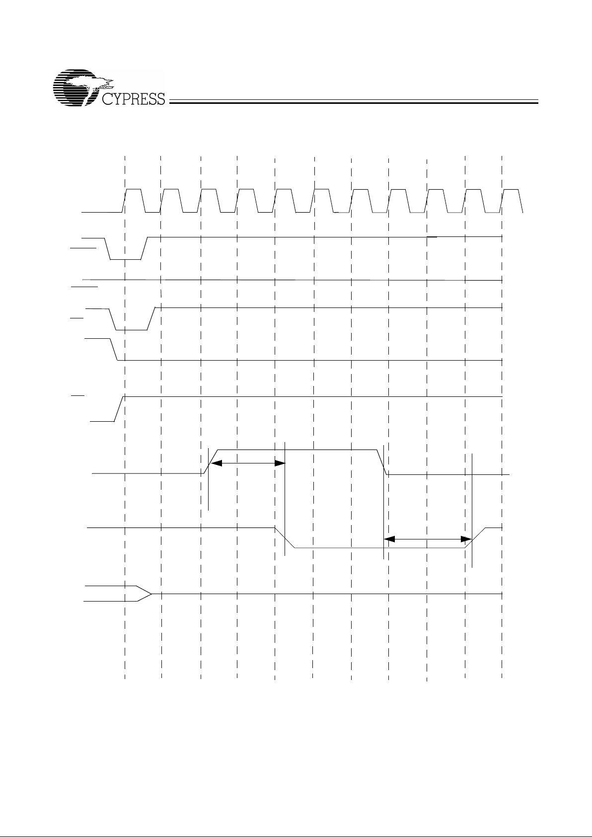
ZZ
t
ZZS
t
ZZREC
I
DD
IDD(active)
Three-state
I/O’s
NotefjdfdhfdjfdfjdjdjdjNo
Notes:
20. Device must be deselected when entering ZZ mode. See Cycle Description Table for all possible signal conditions to deselect the device.
21. I/Os are in three-state when exiting ZZ sleep mode.
ZZ Mode Timing
[20, 21]
CE
2
I
DDZZ
HIGH
Page 15

CY7C1335
© Cypress Semiconductor Corporation, 1999. The information contained herein is subject to change without notice. Cypress Semiconductor Corporation assumes no responsibility for the use
of any circuitry other than circuitry embodied in a Cypress Semiconductor product. Nor does it con vey or imply any license under patent or other rights. Cypress Semiconductor does not authorize
its products for use as critical components in life-support systems where a malfunction or failure may reasonably be expected to result in significant injury to the user. The inclusion of Cypress
Semiconductor products in life-support systems application implies that the manufacturer assumes all risk of such use and in doing so indemnifies Cypress Semiconductor against all charges.
Document #: 38-00452-E
Ordering Information
Speed
(MHz) Orderi ng Code
Package
Name Package Type
Operating
Range
133 CY7C1335-133AC A101 100-Lead Thin Quad Flat Pack Commercial
100 CY7C1335-100AC A101 100-Lead Thin Quad Flat Pack Commercial
75 CY7C1335-75AC A101 100-Lead Thin Quad Flat Pack Commercial
Package Diagram
100-Pin Thin Plastic Quad Flat pack (14 x 20 x 1.4 mm) A101
51-85050-A
 Loading...