

Page 1
f
104
,
ax id:
7
CY7C109
CY7C1009
128K x 8 Static RAM
Features
• High speed
= 10 ns
—t
AA
• Low active power
—1017 mW (max., 12 ns)
• Low CMOS standby power
—55 mW (max.), 4 mW (Low power version)
• 2.0V Data Retention (Low power version)
• Automat ic power-down when desel ected
• TTL-compatible inputs and outputs
• Easy memory expansi on with CE
, CE2, and OE options
1
Functional Description
active HIGH chip enable (CE
(OE
), and three-state drivers. Writing to the device is accomplished by t aking chi p enable one (CE
inputs LOW and chip enable two (CE
the eight I/O pins (I/O
location specifi ed on the address pins (A
0
Reading from the device is accomplished by taking chip enable one (CE
write enable (WE
) and output enable (OE) LOW while forcing
1
) and chip enable two (CE2) HIGH. Under
these conditions, the contents of the memory location specified by the address pins will appear on the I/O pins.
The eight input/output pins (I/O
high-impedance state when the device is deselected (CE
HIGH or CE2 LOW), the outputs are disabled (OE HIGH), or
during a write oper ation ( CE
), an active LOW output enable
2
) and write enable ( WE)
1
) input HIGH. Data on
2
through I/O7) is then written into the
through A16).
0
through I/O7) are placed in a
0
LOW , CE2 HIGH, and W E LOW) .
1
The CY7C109 is available in standard 400-mil-wide SOJ and
The CY7C109 / CY7C1009 is a hig h-performance CMO S static RAM organized as 131,072 words by 8 bits. Easy memory
expans ion i s pro vided b y an a ct ive LO W c hip ena b le (CE
), an
1
32-pin TSOP type I packages. The CY7C1009 is available in
a 300-mil-wide SOJ package. The CY7C1009 and CY7C109
are functionally equivalent in all other respects.
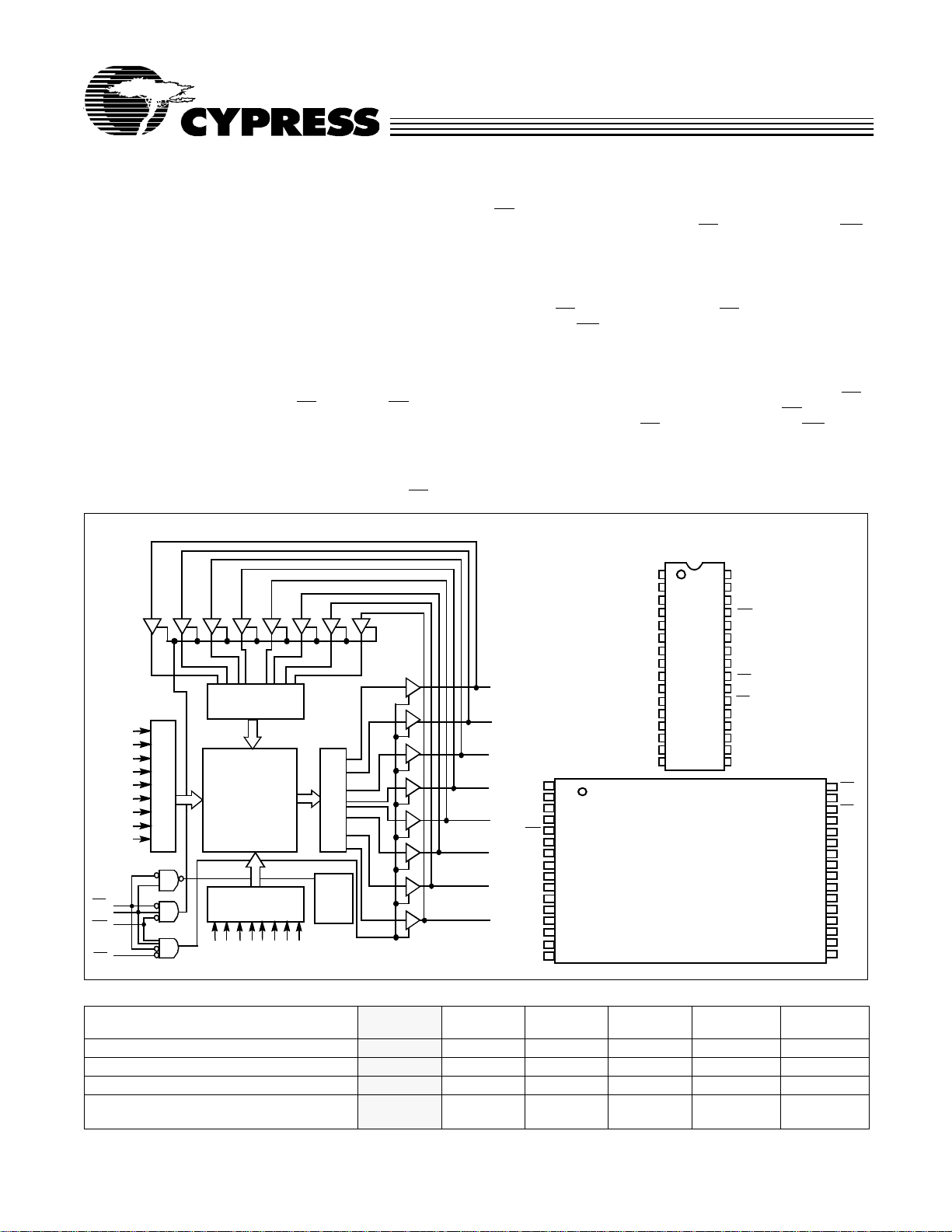
Logic Block Diagram Pin Configurations
SOJ
Top View
V
32
CC
31
A
15
30
CE
2
29
WE
28
A
13
27
A
8
26
A
9
25
A
11
24
OE
23
A
10
22
CE
1
I/O
21
7
I/O
6
20
I/O
5
19
I/O
4
18
I/O
17
3
109–2
32
31
30
29
28
27
26
25
24
23
22
21
20
19
18
17
CE
CE
WE
OE
NC
1
A
16
2
A
3
14
A
4
12
5
A
7
A
6
6
A
5
7
A
8
4
A
9
I/O
109–1
I/O
I/O
I/O
I/O
I/O
I/O
I/O
0
1
2
A
1
11
3
4
5
6
7
CE
V
A
WE
A
NC
A
A
A
2
A
9
3
A
8
4
13
5
6
2
7
15
8
CC
9
10
16
11
14
12
12
A
13
7
A
14
6
15
A
5
16
A
4
INPUT BUFFER
A
0
A
1
A
2
A
3
A
4
A
5
A
6
A
A
1
2
ROW DECODER
7
8
512 x 256 x 8
ARRAY
COLUMN
DECODER
11
10
9
A
A
A
SENSE AMPS
POWER
DOWN
14
15
12
16
A
A
A
A13A
3
A
10
2
A
1
11
A
12
0
I/O
0
13
I/O
1
14
I/O
2
15
GND
16
TSOP I
Top View
(not to scale)
Selection G uide
7C109-10
7C1009-10
Maximum Access Time (ns) 10 12 15 20 25 35
Maximum Operating Current (mA) 195 185 155 140 135 125
Maximum CMOS Standby Current (mA) 10 10 10 10 10 10
Maximum CMOS Standby Current (mA)
2 2 2 — — —
Low Power Version
Shaded areas contain preliminary information.
7C109-12
7C1009-12
7C109-15
7C1009-15
7C109-20
7C1009-20
7C109-25
7C1009-25
7C109-35
7C1009-35
OE
A
CE
I/O
I/O
I/O
I/O
I/O
GND
I/O
I/O
I/O
A
A
A
A
109–3
1
10
7
6
5
4
3
2
1
0
0
1
2
3
Cypress Semiconductor Corporation
• 3901 North First Street • San Jose • CA 95134 • 408-943-2600
June 30
1998
Page 2
CY7C109
CY7C1009
Maximum Ratings
(Abov e which the useful life m ay be impaired. F or user guidelines, not tested.)
Storage Temperature ........................... .. ....–65°C to +150°C
Ambient Temperature with
Power Applied.............................................–55°C to +125°C
Supply Voltage on V
DC V oltage Applied to Outputs
in High Z State
[1]
DC Input Voltage
to Relative GND
CC
....................................–0.5V to VCC + 0.5V
[1]
.................................–0.5V to VCC + 0.5V
Current into Outputs (LOW) .........................................20 mA
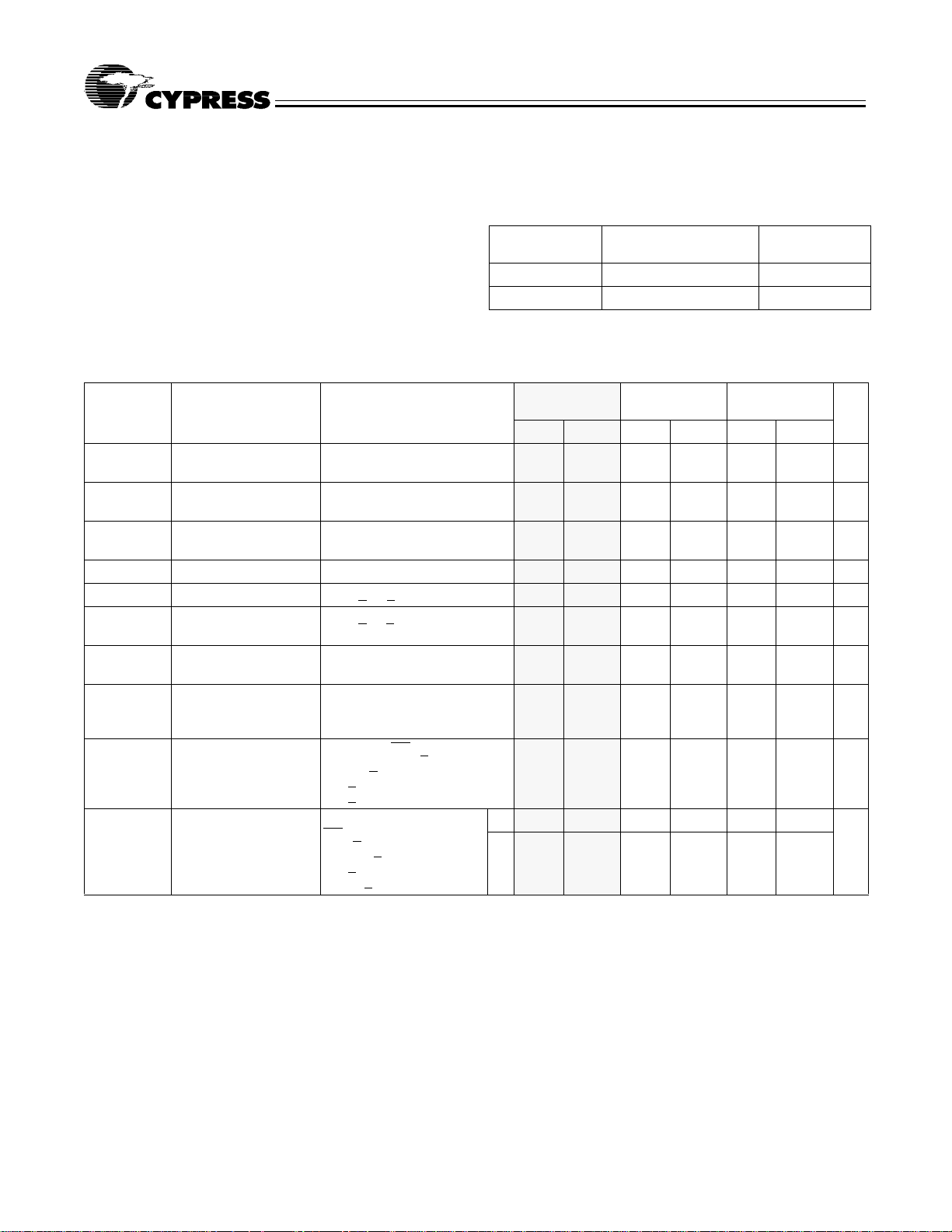
Electrical Characteristics
Parameter Description
V
OH
V
OL
V
IH
V
IL
I
IX
I
OZ
I
OS
I
CC
I
SB1
I
SB2
Shaded areas contain preliminary information.
Output HIGH Voltage VCC = Min.,
Output LOW Voltage VCC = Min.,
Input HIGH Voltage 2.2 V
Input LOW Voltage
Input Load Current GND < VI < V
Output Leakage
Current
Output Short
Circuit Current
[3]
VCC Operating
Supply Current
Automatic CE
Po wer-Down Current
—TTL Inputs
Automatic CE
Po wer-Down Current
—CMOS Inputs
[1]
....–0.5V to +7.0V
Over the Ope rating Range
Tes t Condi tions
I
= –4.0 mA
OH
I
= 8.0 mA
OL
[1]
CC
GND < VI < VCC,
Output Disabled
VCC = Max.,
V
= GND
OUT
VCC = Max.,
I
= 0 mA,
OUT
f = f
MAX
= 1/t
RC
Max. VCC, CE1 > V
or CE2 < VIL,
V
> VIH or
IN
V
< VIL, f = f
IN
MAX
Max. VCC,
CE
> VCC – 0.3V,
1
or CE
< 0.3V,
2
V
> VCC – 0.3V,
IN
or V
< 0.3V, f=0
IN
IH
Static Discharge Voltage .......... ......................... ........>2001V
(per MIL-STD-883, Method 3015)
Latch-Up Current.....................................................>200 mA
Operating Range
Ambient
Range
Temperature
Commercial 0°C to +70°C 5V ± 10%
Industrial
[3]
7C109-10
7C1009-10
−40°C to +85°C
7C109-12
7C1009-12
Min. Max. Min. Max. Min. Max. Unit
2.4 2.4 2.4 V
0.4 0.4 0.4 V
CC
+ 0.3
2.2 V
–0.3 0.8 –0.3 0.8 –0.3 0.8 V
–1 +1 –1 +1 –1 +1 µA
–5 +5 –5 +5 –5 +5 µA
–300 –300 –300 mA
195 185 155 mA
45 45 40 mA
10 10 10 mA
L
222
CC
+ 0.3
[2]
7C109-15
7C1009–15
2.2 V
V
CC
5V ± 10%
CC
+ 0.3
V
2
Page 3
CY7C109
CY7C1009
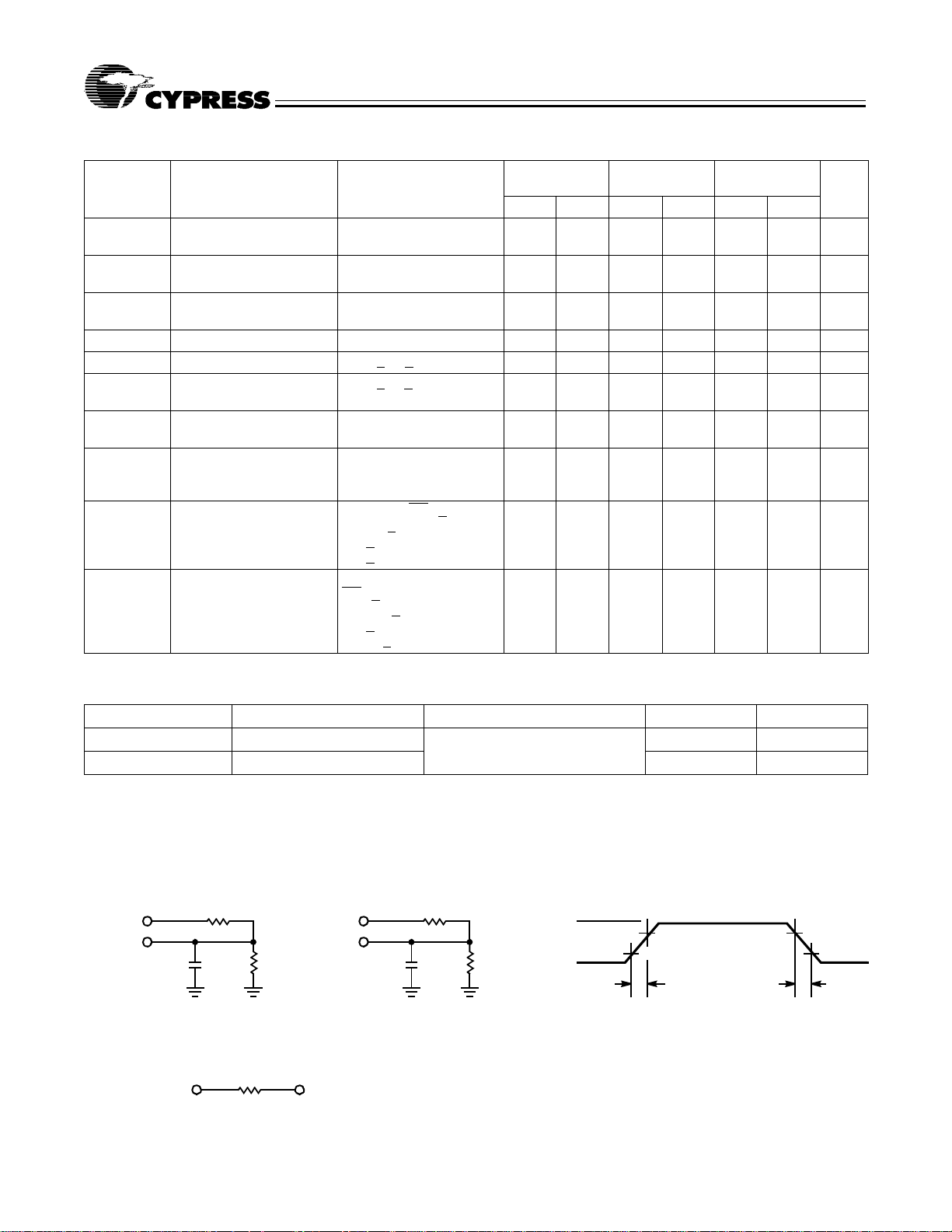
Electrical Characteristics
Over the Ope rating Range (continued)
7C109-20
7C1009-20
7C109-25
7C1009-25
7C109-35
7C1009-35
Parameter Description Test Conditions Min. Max. Min. M ax. Min. Max. Unit
V
V
V
V
I
IX
I
OZ
I
OS
I
CC
I
SB1
I
SB2
OH
OL
IH
IL
Output HIGH Voltage VCC = Min.,
I
= –4.0 mA
OH
2.4 2.4 2.4 V
Output LO W Voltage VCC = Min.,
I
= 8.0 mA
OL
Input HIGH Voltage 2.2 V
+ 0.3
Input LOW Voltage
Input Load Curren t GND < VI < V
Output Leakage
Current
Output Short
Circuit Current
VCC Operating
Supply Current
Automatic CE
Po wer-Down Current
—TTL Inputs
Automatic CE
Po wer-Down Current
—CMO S Inputs
[1]
CC
GND < VI < VCC,
–0.3 0.8 –0.3 0.8 –0.3 0.8 V
–1 +1 –1 +1 –1 +1 µA
–5 +5 –5 +5 –5 +5 µA
Output Disabled
[3]
VCC = Max.,
V
= GND
OUT
VCC = Max.,
I
= 0 mA,
OUT
f = f
MAX
= 1/t
RC
Max. VCC, CE1 > V
or CE2 < VIL,
V
> VIH or
IN
V
< VIL, f = f
IN
MAX
IH
–300 –300 –300 mA
Max. VCC,
CE
> VCC – 0.3V,
1
or CE
< 0.3V,
2
V
> VCC – 0.3V,
IN
or V
< 0.3V, f=0
IN
0.4 0.4 0.4 V
CC
2.2 V
+ 0.3
CC
2.2 V
CC
+ 0.3
140 135 125 mA
30 30 25 mA
10 10 10 mA
V
Capacitance
[4]
Parameter Description Te st Conditions Max. Unit
C
IN
C
OUT
Notes:
1. V
(min.) = –2.0V for pulse durations of less than 20 ns .
IL
is the “instant on” case temperature.
2. T
A
3. Not more than one output should be shorted at one time. Duration of the short circuit should not exceed 30 seconds.
4. Tested initially and after any design or process changes that may affect these parameters.
Input Capacitance TA = 25°C, f = 1 MHz,
V
= 5.0V
Output Capacitance 8 pF
CC
9pF
AC Test Loads and Waveforms
R1 480
5V
OUTPUT
30 pF
INCLUDING
JIG AND
SCOPE
Equivalent to: VENIN EQUIVALENT
OUTPUT
(a)
THÉ
Ω
167
OUTPUT
R2
255
Ω
Ω
1.73V
5V
5 pF
INCLUDING
JIG AND
SCOPE
(b)
R1 480
Ω
109–3
R2
255
3.0V
GND
Ω
3ns
≤
ALL INPUT PULSES
90%
10%
90%
10%
≤
109–4
ns
3
3
Page 4

Switching C h aracteri sti cs
[3, 5]
Over the Operating Range
CY7C109
CY7C1009
Parameter Description
7C109-10
7C1009-10
Min. Max. Min. Max. Min. Max. Unit
7C109-12
7C1009-12
7C109-15
7C1009-15
READ CYCLE
t
RC
t
AA
t
OHA
t
ACE
t
DOE
t
LZOE
t
HZOE
t
LZCE
t
HZCE
t
PU
Read Cycle Time 10 12 15 ns
Address to Data Valid 10 12 15 ns
Data Hold from Address Change 3 33ns
CE1 LOW to Data Valid, CE2 HIGH to Data
10 12 15 ns
Valid
OE LOW to Data Valid 567ns
OE LOW to Low Z 0 00ns
OE HIGH to High Z
CE1 LOW to Low Z, CE2 HIGH to Low Z
CE1 HIGH to High Z, CE2 LOW to High Z
CE1 LOW to Power-Up, CE2 HIGH to
[6, 7]
[7]
[6, 7]
567ns
3 33ns
567ns
0 00ns
Power-Up
t
PD
WRITE CYCLE
t
WC
t
SCE
t
AW
t
HA
t
SA
t
PWE
t
SD
t
HD
t
LZWE
t
HZWE
Shaded areas contain preliminary information.
Notes:
5. Test conditions assume signal transition time of 3 ns or less, timing reference levels of 1.5V, input pulse levels of 0 to 3.0V, and output loading of the specified
I
OL/IOH
6. t
HZOE
7. At any given temperature and voltage condition, t
8. The internal write time of the memory is defined by the overlap of CE
and the trans ition of a ny of thes e signal s can te rminate the write. T he inpu t data set-u p and hold timi ng should be r ef erenced to the lead in g edge of th e signal that terminates
the write.
9. The minimum write cycle time for Write Cycle no. 3 (WE
CE1 HIGH to Power-Down, CE2 LOW to
10 12 15 ns
Power-Down
[8,9]
Write Cycle Time 10 12 15 ns
CE1 LOW to Write End, CE2 HIGH to Write End 8 10 12 ns
Address Set-Up to Write End 8 10 12 ns
Address Hold from Write End 0 00ns
Address Set-Up to Write Start 0 00ns
WE Pulse Width 8 10 12 ns
Data Se t- U p to Write End 6 78ns
Data Hold from Write End 0 00ns
WE HIGH to Low Z
WE LOW to High Z
and 30-pF load capac itance.
, t
HZCE
, and t
are specified wi th a loa d capac itance of 5 pF as in part (b) of A C Test Loads. Transition is measured ±500 mV from steady- state v ol tage.
HZWE
[7]
[6, 7]
is less than t
HZCE
controlled, OE LOW) is the sum of t
, t
LZCE
HZOE
LOW , C E2 HIGH, and WE LO W. CE1 and WE must be LO W an d CE2 HIGH to init iate a write ,
1
3 33ns
567ns
is less than t
LZOE
, and t
HZWE
is less than t
HZWE
and TSD.
for any given device.
LZWE
4
Page 5

Switching Characteristics
[3, 5]
Over the Operating Range
CY7C109
CY7C1009
Parameter Description
READ CYCLE
t
RC
t
AA
t
OHA
t
ACE
t
DOE
t
LZOE
t
HZOE
t
LZCE
t
HZCE
t
PU
t
PD
WRITE CYCLE
t
WC
t
SCE
t
AW
t
HA
t
SA
t
PWE
t
SD
t
HD
t
LZWE
t
HZWE
Read Cycle Time 20 25 35 ns
Address to Data Valid 20 25 35 ns
Data Hold from Address Change 3 5 5 ns
CE1 LOW to Data Valid, CE2 HIGH to Data
Valid
OE LOW to Data Valid 8 10 15 ns
OE LOW to Low Z 0 0 0 ns
OE HIGH to High Z
[6, 7]
CE1 LOW to Low Z, CE2 HIGH to Low Z
CE1 HIGH to High Z, CE2 LOW to High Z
CE1 LOW to Power-Up, CE2 HIGH to
Po wer-Up
CE1 HIGH to Power-Down, CE2 LOW to
Power-Down
[8]
Write Cycle Time 20 25 35 ns
CE1 LOW to Write End, CE2 HIGH to Write End 15 20 25 ns
Address Set-Up to Write End 15 20 25 ns
Address Hold from Write End 0 0 0 ns
Address Set-Up to Write Start 0 0 0 ns
WE Pulse Width 12 15 20 ns
Data Set-Up to Write End 10 15 20 ns
Data Hold from Write End 0 0 0 ns
WE HIGH to Low Z
WE LOW to High Z
[7]
[6, 7]
Data Retention Characteristics
7C109-20
7C1009-20
20 25 35 ns
81015ns
[7]
[6, 7]
355ns
81015ns
000ns
20 25 35 ns
355ns
81015ns
Over the Operating Range (L Version Only)
7C109-25
7C1009-25
7C109-35
7C1009-35
UnitMin. Max. Min. Max. Min. Min.
Parameter Description Conditions Min. Max Unit
V
DR
I
CCDR
t
CDR
t
R
Shaded areas contain preliminary information.
VCC for Data Reten ti on No input may e xceed VCC + 0.5V
Data Retention Current 50 µA
Chip Deselect to Data Retention Time 0 ns
Operation Recov ery Time t
V
= VDR = 2.0V,
CC
CE
> VCC – 0.3V or CE2 < 0.3V,
1
V
> VCC – 0.3V or VIN < 0.3V
IN
2.0 V
RC
ns
5
Page 6

Data Retention Waveform
V
CC
CE
Switching Waveforms
Read Cycle No. 1
ADDRESS
DATA OUT
[10, 11]
PREVIOUS DATA VALID DATA VALID
t
OHA
t
CDR
CY7C109
CY7C1009
DAT A RETENTION MODE
VDR> 2V
t
RC
t
AA
4.5V4.5V
t
R
109-5
109–6
Read Cycle No. 2 (OE Controlled)
ADDRESS
CE
1
CE
2
OE
DA TA OUT
V
CC
SUPPLY
CURRENT
Notes:
10. Device is continuously selected. OE
11. WE
is HIGH for read cycle.
12. Address valid prior to or coincident with CE
HIGH IMPEDANCE
t
LZCE
t
PU
, CE1 = VIL, CE2 = VIH.
[11, 12]
t
RC
t
ACE
t
DOE
t
LZOE
50%
transition LOW and CE2 transition HIGH.
1
DATA VALID
t
HZOE
t
HZCE
HIGH
IMPEDANCE
t
PD
ICC
50%
ISB
109–7
6
Page 7

CY7C109
CY7C1009
Switching Waveforms
Write Cycle No. 1 (CE
(continued )
or CE2 Controlled)
1
[13, 14]
ADDRESS
CE
1
t
CE
2
SA
t
AW
WE
DATA I/O
Write Cycle No. 2 (WE Controlled, OE HIGH During Write)
ADDRESS
t
WC
[13, 14]
t
WC
t
PWE
t
SCE
t
SCE
t
SD
DATA VALID
t
HA
t
HD
109–8
CE
1
CE
2
WE
OE
DATA I/O
Notes:
13. Data I/O is high impedance if OE
14. If CE
goes HIGH or CE2 goes LOW si multane ously w ith WE going HIGH, t he out put remai ns in a hi gh-impedanc e state .
1
NOTE 15
= VIH.
t
SA
t
HZOE
t
SCE
t
SCE
t
AW
t
PWE
t
SD
t
HA
t
HD
DATAINVALID
109–9
7
Page 8

CY7C109
CY7C1009
Switching Waveforms
Write Cycle No. 3 (WE
ADDRESS
CE
1
CE
2
WE
DATA I/O
Note:
15. During this period the I/Os are in the output state and input signals should not be applied.
NOTE
(continued )
Controlled, OE LOW)
t
SA
15
t
HZWE
[14]
t
AW
t
SCE
t
SCE
t
WC
t
PWE
t
SD
DATA VALID
t
HA
t
LZWE
t
HD
109–9
Truth Table
CE
H X X X High Z Po wer-Down Standby (ISB)
X L X X High Z Power-Down Standby (ISB)
L H L H Data Out Read Active (ICC)
L H X L Data In Write Active (ICC)
L H H H High Z Selected, Outputs Disabled Active (ICC)
CE
1
OE WE I/O0 – I/O
2
7
Mode Power
8
Page 9

Ordering Information
Speed
(ns) Ordering Code
10 CY7C109-10VC V33 32-Lead (400-Mil) Molded SOJ Commercial
CY7C1009-10VC V32 32-Lead (300-Mil) Molde d SOJ
CY7C1009L-10VC V32 32-Lead (300-Mil) Molded SOJ
12 CY7C109-12VC V33 32-Lead (400-Mil) Molded SOJ
CY7C1009-12VC V32 32-Lead (300-Mil) Molded SOJ
CY7C1009L-12VC V32 32-Lead (300-Mil) Molded SOJ
CY7C109-12ZC Z32 32-Lead TSOP Type I
15 CY7C109–15VC V33 32-Lead (400-Mil) Molded SOJ
CY7C1009-15VC V32 32-Lead (300-Mil) Molded SOJ
CY7C1009L-15VC V32 32-Lead (300-Mil) Molded SOJ
CY7C109–15ZC Z32 32-Lead TSOP Type I
20 CY7C109–20VC V33 32-Lead (400-Mil) Molded SOJ
CY7C1009-20VC V32 32-Lead (300-Mil) Molded SOJ
CY7C109–20VI V33 32-Lead (400-Mil) Molded SOJ Industrial
CY7C109–20ZC Z32 32-Lead TSOP Type I Commercial
CY7C109-20ZI Z32 32-Lead TSOP Type I Industrial
25 CY7C109–25VC V33 32-Lead (400-Mil) Molded SOJ Commercial
CY7C1009-25VC V32 32-Lead (300-Mil) Molded SOJ
CY7C109–25VI V33 32-Lead (400-Mil) Molded SOJ Industrial
CY7C109–25ZC Z32 32-Lead TSOP Type I Commercial
CY7C109-25ZI Z32 32-Lead TSOP Type I Industrial
35 CY7C109–35VC V33 32-Lead (400-Mil) Molded SOJ Commercial
CY7C1009-35VC V32 32-Lead (300-Mil) Molded SOJ
CY7C109–35VI V33 32-Lead (400-Mil) Molded SOJ Industrial
Shaded areas contain preliminary information.
Package
Name Package Type
CY7C109
CY7C1009
Operating
Range
Document #: 38–00140–J
9
Page 10
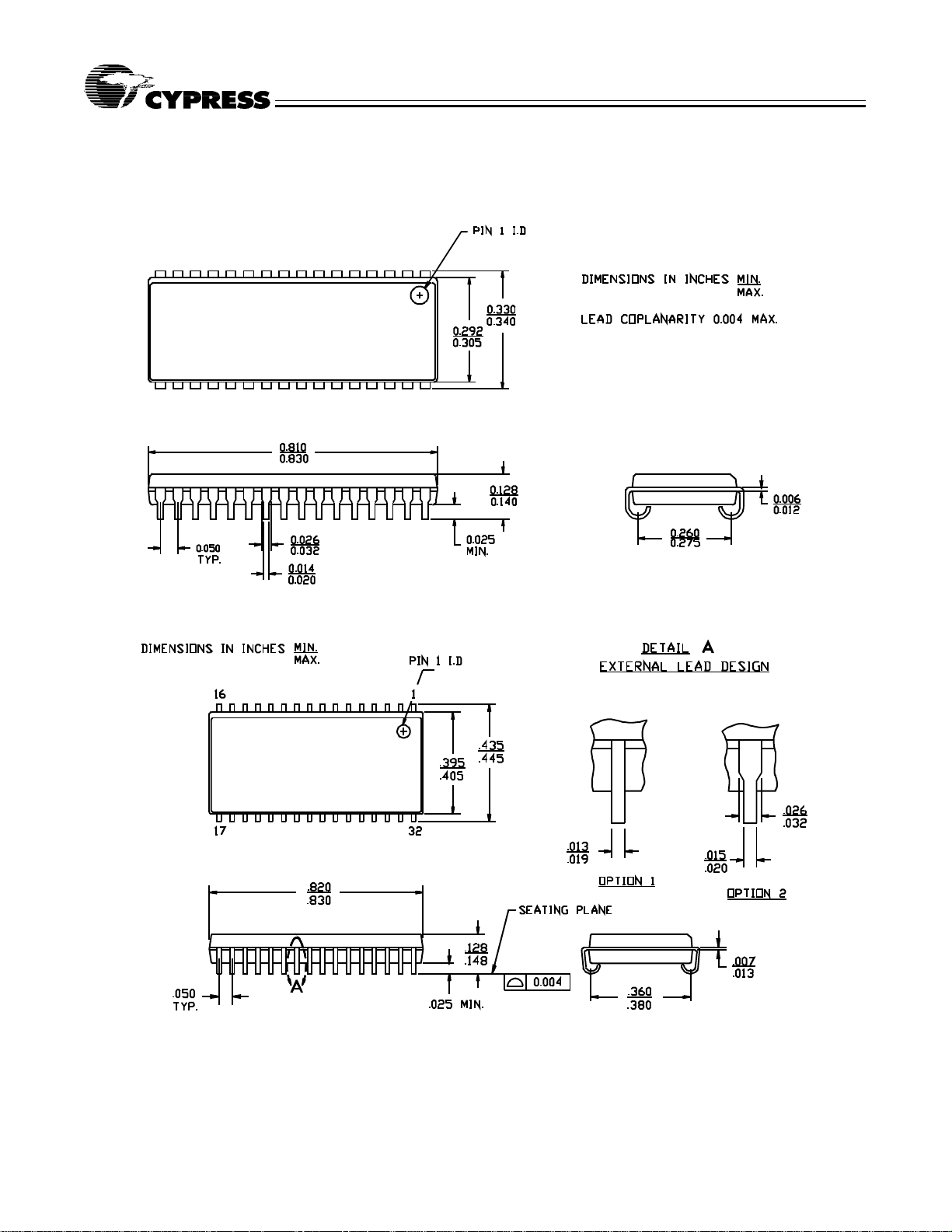
Package Diagrams
CY7C109
CY7C1009
32-Lead (300-Mil) Molded SOJ V32
32-Lead (400-Mil) Molded SOJ V33
51-85041-A
51-85033-A
10
Page 11

CY7C109
CY7C1009
Package Diagrams
(continued)
32-Lead Thin Small Outline Package Z32
51-85056-B
© Cypress Semiconductor Corporation, 1998. The information contained herein is subject to change without notice. Cypress Semiconductor Corporation assumes no responsibility for the use
of any circuitry other than circuitry embodied in a Cypress Semiconductor product. Nor does it convey or imply any lice nse under patent or other rights. Cypress Semi conductor does not authorize
its products for use as critical components in life-support systems where a malfunction or failure may reasonably be expected to result in significant injury to the user. The inclusion of Cypress
Semiconductor products in life-support systems application implies that the manufacturer assumes all risk of such use and in doing so indemnifies Cypress Semiconductor against all charges.
 Loading...