

Page 1
CY7C1041
256K x 16 Static RAM
Features
written into the location specified on the address pins (A
through A17). If Byte High Enable (BHE) is LOW, then data
• High speed
= 15 ns
—t
AA
• Low active power
—1430 mW (max.)
• Low CMOS standby power (L version)
—2.75 mW (max.)
2.0V Data Retention (400 µW at 2.0V retention)
•
• Automat ic power-down when desel ected
• TTL-compatible inputs and outputs
• Easy memory expansion with CE
and OE fe atures
Functional Description
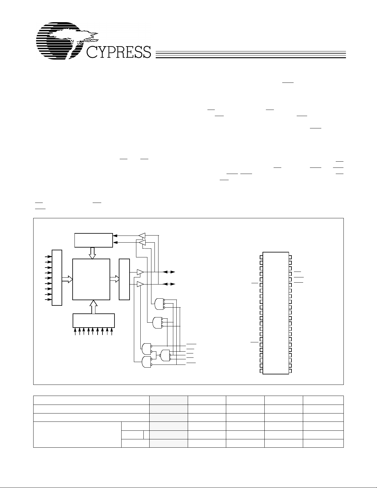
The CY7C1041 is a high-performance CMOS static RAM organized as 262,144 words by 16 bits.
Writing to the device is accomplished by taking Chip Enable
(CE
) and Write Enable (WE) inputs LOW. If Byte Low Enable
(BLE
) is LOW, then data from I/O pins (I/O0 through I/O7), is
from I/O pins (I/O
specified on the address pins (A
throug h I/O15) is written into the location
8
through A17).
0
Reading from the device is accomplished by taking Chip Enable (CE
Enable (WE
) and Output Enable (O E) LOW whil e for cing the Write
) HIGH. If Byte Low Enable (BLE) is LOW, then
data from the memory location specified by the address pins
will appear on I/O
to I/O7. If Byte High Enable (BHE) is LOW,
0
then data from memory will appear on I/O
truth table a t the bac k of this dat a sheet f or a c omplete des cription of read and write modes.
The input/output pins (I/O
high-impedance state when the device is deselected (CE
through I/O15) are placed in a
0
HIGH), the outputs are di sabled (OE HIG H), the BHE and BLE
are disabl ed (BHE, BLE HIGH), or during a write operation (CE
LOW, and WE LOW).
The CY7C1041 is available in a standard 44-pin 4 00-mil-wide
body width SOJ and 44- pin TSO P II pac kage wi th cent er power and ground (re volutionary) pinout.
Logic Block Diagram Pin Configuration
A
A
A
A
A
CC
SS
A
A
A
A
A
0
1
2
3
4
0
1
2
3
4
5
6
7
5
6
7
8
9
SOJ
TSOP II
Top View
1
2
3
4
5
6
7
8
9
10
11
12
13
14
15
16
17
18
19
20
21
22
44
43
42
41
40
39
38
37
36
35
34
33
32
31
30
29
28
27
26
25
24
23
INPUT BUFFER
A
0
A
1
A
2
A
3
A
4
A
5
A
A
A
ROW DECODER
6
7
8
256K x 16
ARRAY
1024 x 4096
SENSE AMPS
I/O0 – I/O
I/O8 – I/O
7
15
CE
I/O
I/O
I/O
I/O
V
COLUMN
DECODER
V
I/O
I/O
11
14
15
12
A13A
AAA
16
17
A
BHE
WE
CE
OE
9
10
A
A
A
I/O
I/O
WE
BLE
1041–1
to I/O15. See the
8
A
17
A
16
A
15
OE
BHE
BLE
I/O
15
I/O
14
I/O
13
I/O
12
V
SS
V
CC
I/O
11
I/O
10
I/O
9
I/O
8
NC
A
14
A
13
A
12
A
11
A
10
1041–2
0
Selection G uide
7C1041-12 7C1041-15 7C1041-17 7C1041-20 7C1041-25
Maximum Access Time (ns) 12 15 17 20 25
Maximum Operating Current (mA) 280 260 250 230 220
Maximum CMOS Standby Current
(mA)
Shaded areas contain preliminary information.
Cypress Semiconductor Corporation
Com’l 333 3 3
Com’l L 0.5 0.5 0.5 0.5 0.5
Ind’l 666 6 6
• 3901 North First Street • San Jose • CA 95134 • 408-943-2600
October 4, 1999
Page 2
Maximum Ratings
(Abov e which the useful lif e m ay be impaired. For user guidelines, not tested.)
Storage Temperature .............................. .. .–65°C to +150°C
Ambient Temperature with
Power Applied.............................................–55°C to +125°C
Supply Voltage on VCC to Relative GND
DC Voltage Applied to Outputs
in High Z State
[1]
....................................–0.5V to VCC + 0.5V
[1]
....–0.5V to +7.0V
CY7C1041
[1]
DC Input Voltage
Curre n t in to Out p ut s (L OW )............... .......................... 20 mA
Operating Range
Range
Commercial 0°C to +70 °C 5V ± 0.5
Industrial –40°C to +85°C
................................ –0.5V to VCC + 0.5V
Ambient
Temperature
[2]
V
CC
Electrical Characteristics
Over the Operating Range
Parameter Description Test Condi ti ons
V
OH
V
OL
V
IH
V
IL
I
IX
I
OZ
I
CC
I
SB1
I
SB2
Shaded areas contain preliminar y information.
Notes:
1. V
2. T
A
Output HIGH Voltage VCC = Min., IOH = –4.0 mA 2.4 2.4 2.4 V
Output LO W Voltage VCC = Min., IOL = 8.0 mA 0.4 0.4 0.4 V
Input HIGH Voltage 2.2 V
Input LOW Voltage
Input Load Current GND < VI < V
Output Leakage
Current
VCC Operating
Supply Current
Automatic CE
Po wer-Down Current
—TTL Inputs
Automatic CE
Po wer-Down Current
—CMOS Inputs
(min.) = –2.0V f or pulse durati ons of less t han 20 ns.
IL
is the case temper ature .
[1]
GND < V
Output Disabled
VCC = Max.,
f = f
MAX
Max. VCC, CE > V
VIN > VIH or
V
< VIL, f = f
IN
Max. VCC,
CE
> VCC – 0.3V,
V
> VCC – 0.3V,
IN
or V
< 0.3V, f = 0
IN
OUT
= 1/t
CC
< VCC,
RC
IH
MAX
Com’l
Com’lL
Ind’l
7C1041-12 7C1041-15 7C1041-17
Min. Max. Min. Max. Min. Max. Unit
CC
+ 0.5
2.2 V
CC
+ 0.5
2.2 V
CC
+ 0.5
V
–0.5 0.8 –0.5 0.8 –0.5 0.8 V
–1 +1 –1+1–1+1µA
–1 +1 –1+1–1+1µA
280 260 250 mA
40 40 40 mA
333mA
0.5 0.5 0.5 mA
666mA
2
Page 3
CY7C1041
Electrical Characteristics
Over the Operating Range (continued)
Test Condi tions 7C1041-20 7C1041-25
Parameter Description Min. Max. Min. Max. Uni t
V
OH
V
OL
V
IH
V
IL
I
IX
I
OZ
I
CC
I
SB1
I
SB2
Capacitance
Output HIGH Voltage VCC = Min., IOH = –4.0 mA 2.4 2.4 V
Output LOW Voltage VCC = Min., IOL = 8.0 mA 0.4 0.4 V
Input HIGH Voltage 2.2 V
Input LOW Voltage
Input Load Current GND < VI < V
Output Leakage
Current
VCC Operating
Supply Current
Autom atic C E
Po wer-Down Current
—TTL Inpu ts
Autom atic C E
Po wer-Down Current
—CMOS Inputs
[3]
[1]
GND < V
Output Disabled
VCC = Max.,
f = f
Max. V
VIN > VIH or
V
IN
Max. VCC,
CE
V
IN
or V
CC
< VCC,
OUT
= 1/t
MAX
< VIL, f = f
, CE > V
CC
RC
MAX
> VCC – 0.3V,
> VCC – 0.3V,
< 0.3V, f = 0
IN
–0.5 0.8 –0.5 0.8 V
–1+1–1+1µA
–1+1–1+1µA
IH
Com’l33mA
Com’lL 0.5 0.5 mA
Ind’l66mA
CC
+ 0.5
2.2 V
230 220 mA
40 40 mA
+ 0.5 V
CC
Parameter Description Te st Conditions Max. Unit
C
IN
C
OUT
Note:
3. Tested initially and after any design or process changes that may affect these parameters.
Input Capacitance TA = 25°C, f = 1 MHz,
V
= 5.0V
I/O Capacitance 8 pF
CC
8pF
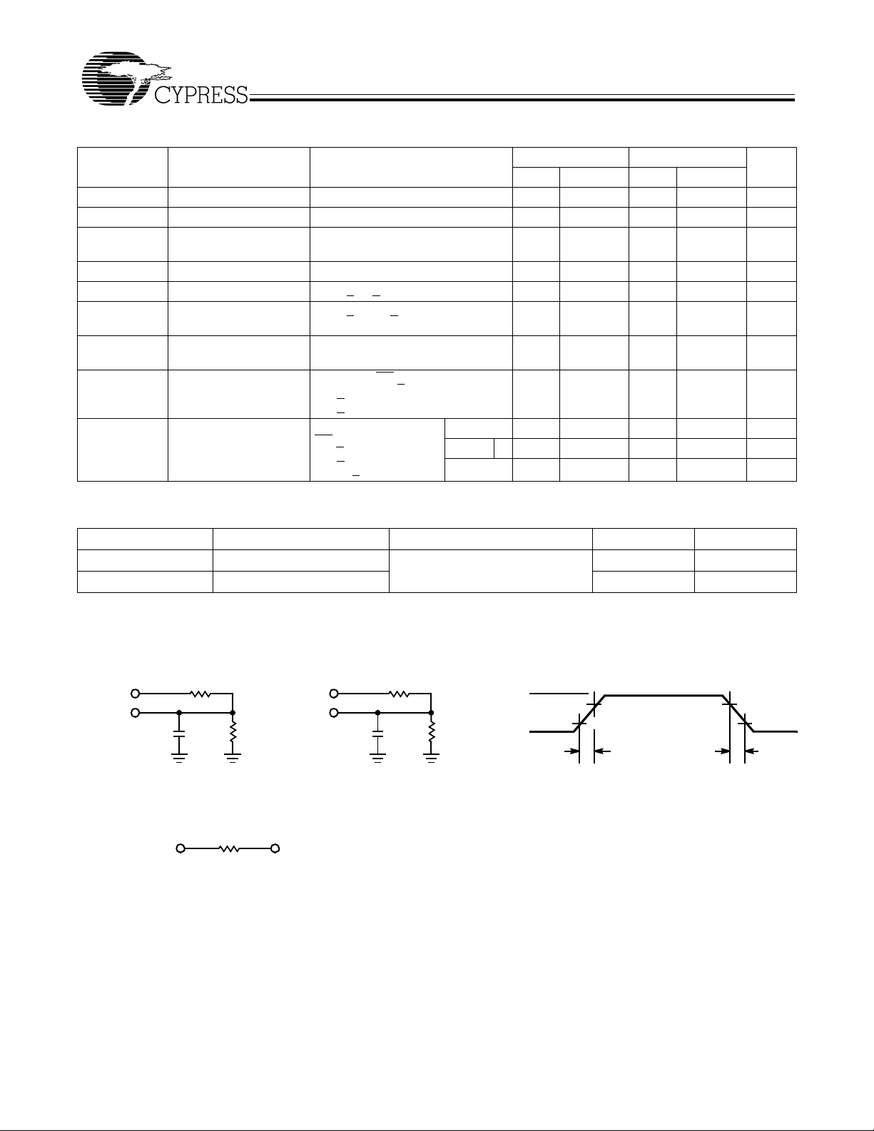
AC Test Loads and Waveforms
R1 481
THÉ
Ω
167
OUTPUT
R2
255
Ω
Ω
1.73V
5V
OUTPUT
30 pF
INCLUDING
JIG AND
SCOPE
Equivalent to: VENIN EQUIVALENT
OUTPUT
(a)
5V
5 pF
INCLUDING
JIG AND
SCOPE
R1 481
(b)
Ω
1041–3
R2
255
3.0V
GND
Ω
≤
3 ns
ALL INPUT PULSES
90%
10%
90%
10%
≤
1041–4
3
ns
3
Page 4
CY7C1041
[4]
Switching Characteristics
Parameter Description
READ CYCLE
t
RC
t
AA
t
OHA
t
ACE
t
DOE
t
LZOE
t
HZOE
t
LZCE
t
HZCE
t
PU
t
PD
t
DBE
t
LZBE
t
HZBE
WRITE CYCLE
t
WC
t
SCE
t
AW
t
HA
t
SA
t
PWE
t
SD
t
HD
t
LZWE
t
HZWE
t
BW
Shaded areas contain preliminary information.
Notes:
4. T est conditions assume signal transition time of 3 ns or less, timing reference levels of 1.5V , input pulse levels of 0 to 3.0V, and output loading of the specified
I
OL/IOH
5. t
HZOE
6. At any given temperature and voltage condition, t
7. The internal write time of the memory is defined by the overlap of CE
these signals can terminate the w rite. The input d ata s et-up a nd hold t im ing shoul d be refe renced to th e leading e dge of the s ignal t hat te rminates the write.
8. The minimum write cycle time for Write Cycle No. 3 (WE
Read Cycle Time 12 15 17 ns
Address to Data Valid 12 15 17 ns
Data Hold from Address Change 3 33ns
CE LOW to Data Valid 12 15 17 ns
OE LOW to Data Va lid 677ns
OE LOW to Low Z 0 00ns
OE HIGH to High Z
CE LOW to Low Z
CE HIGH to High Z
CE LOW to Po wer-Up 0 00ns
CE HIGH to Power-Down 12 15 17 ns
Byte Ena bl e to Dat a Valid 677ns
Byte Ena bl e to Low Z 0 00ns
Byte Disable to High Z 677ns
[7, 8]
Write Cycle Time 12 15 17 ns
CE LOW to Write End 10 12 14 ns
Address Set-Up to Write End 10 12 14 ns
Address Hold from Write End 0 00ns
Address Set-Up to Write Start 0 00ns
WE Pulse Widt h 10 12 14 ns
Data Se t- U p to Write End 7 88ns
Data Hold from Write End 0 00ns
WE HIGH to Low Z
WE LOW to High Z
Byte Enable to End of Write 10 12 12 ns
and 30-pF load ca pacitanc e.
, t
HZCE
, and t
are specified wi th a loa d capac itance of 5 pF as i n part (b) of A C Test Loads. Transition is measured ±500 mV from steady- state v ol tage .
HZWE
Over the Operating Range
[5, 6]
[6]
[5, 6]
[6]
[5, 6]
is less than t
HZCE
controlled, OE LOW) is the sum of t
7C1041-12 7C1041-15 7C1041-17
Min. Max. Min. Max. Min. M ax. Unit
677ns
3 33ns
677ns
3 33ns
677ns
, t
LZCE
is less than t
HZOE
LOW , and W E LOW. CE and WE must be LOW to initi ate a write, and th e tr ansiti on o f either of
LZOE
, and t
HZWE
is less than t
HZWE
and tSD.
for any given device.
LZWE
4
Page 5

[4]
Switching Characteristics
Over the Operating Range (continued)
Parameter Description
READ CYCLE
t
RC
t
AA
t
OHA
t
ACE
t
DOE
t
LZOE
t
HZOE
t
LZCE
t
HZCE
t
PU
t
PD
t
DBE
t
LZBE
t
HZBE
WRITE CYCLE
t
WC
t
SCE
t
AW
t
HA
t
SA
t
PWE
t
SD
t
HD
t
LZWE
t
HZWE
t
BW
Read Cycle Time 20 25 ns
Address to Data Valid 20 25 ns
Data Hold from Address Change 3 5 ns
CE LOW to Data Valid 20 25 ns
OE LOW to Data Valid 8 10 ns
OE LOW to Low Z 0 0 ns
OE HIGH to High Z
CE LOW to Low Z
CE HIGH to High Z
[5, 6]
[6]
[5, 6]
CE LOW to Power-Up 0 0 ns
CE HIGH to Power-Down 20 25 ns
Byte Enable to Data Valid 8 10 ns
Byte Enable to Low Z 0 0 ns
Byte Disable to High Z 8 10 ns
[7, 8]
Write Cycle Time 20 25 ns
CE LOW to Write End 13 15 ns
Address Set-Up to Write End 13 15 ns
Address Hold from Write End 0 0 ns
Address Set-Up to Write Start 0 0 ns
WE Pulse Width 13 15 ns
Data Set-Up to Write End 9 10 ns
Data Hold from Write End 0 0 ns
WE HIGH to Low Z
WE LOW to High Z
[6]
[5, 6]
Byte Enable to End of Write 13 15 ns
CY7C1041
7C1041-20 7C1041-25
UnitMin. Max. Min. Max.
810ns
35ns
810ns
35ns
810ns
Data Rete n ti o n C h ar acteristic s
Over the Operating Range
Parameter Description Conditions
V
DR
I
CCDR
[3]
t
CDR
[9]
t
R
Notes:
9. t
< 100 µs for all s peeds.
r
10. No input may exceed V
VCC for Da ta Rete ntion 2.0 V
Data Retention Current VCC = VDR = 2.0V ,
CE
Com’l L 200
> VCC – 0.3V ,
V
> VCC – 0.3V or VIN < 0.3V
IN
Chip Deselect to Data Retention Time 0 ns
Operation Recov ery Time See Note 9
+ 0.5V.
CC
5
[10]
Min. Max. Unit
µA
µA
µA
Page 6

Data Retention Waveform
V
CC
CE
Switchin g W aveforms
t
CDR
CY7C1041
DATA RETENTION MODE
VDR> 2V
3.0V3.0V
t
R
1041–5
Read Cycle No.1
[11, 12]
ADDRESS
DATA OUT
PREVIOUS DATA VALID DATA VALID
Read Cycle No.2 (OEControlled)
ADDRESS
CE
OE
BHE, BLE
DATA OUT
V
CC
SUPPLY
CURRENT
HIGH IMPEDANCE
t
LZCE
t
PU
[12, 13]
t
ACE
t
DOE
t
LZOE
t
DBE
t
LZBE
t
OHA
50%
t
RC
t
AA
1041-6
t
RC
t
HZOE
t
HZCE
t
DATA VALID
HZBE
t
PD
HIGH
IMPEDANCE
I
ICC
CC
50%
ISB
I
SB
1041-7
Notes:
11. Device is continuously selected. OE
is HIGH for read cycle.
12. WE
13. Address valid prior to or coincident with CE tr ansitio n LO W.
, CE, BHE, and/or BHE = VIL.
6
Page 7

CY7C1041
Switchin g W aveforms
Write Cycle No. 1 (CE
ADDRESS
CE
WE
BHE, BLE
DATAI /O
Controlled)
(continued)
[14, 15]
t
SA
t
AW
t
WC
t
SCE
t
PWE
t
BW
t
HA
t
SD
t
HD
1041-8
WriteCycleNo. 2 (BLEorBHE Controlled)
ADDRESS
t
,BLE
BHE
WE
CE
DATAI/O
Notes:
14. Data I/O is high impedance if OE
15. If CE
goes HIGH simu ltaneousl y with WE g oing HI GH, the output remain s in a hi gh-i mpedance state.
SA
or BHE and/or BL E= VIH.
t
WC
t
BW
t
AW
t
PWE
t
SCE
t
SD
t
HA
t
HD
1041-9
7
Page 8

CY7C1041
Switchin g W aveforms
Write Cycle No.3
ADDRESS
CE
WE
BHE
,BLE
DATA I/O
Controlled, LOW)
(WE
(continued)
t
SA
t
AW
t
SCE
t
WC
t
BW
t
HZWE
t
PWE
t
HA
t
SD
t
HD
t
LZWE
1041-10
Truth Table
CE OE WE BLE BHE I/O0–I/O
7
H X X X X High Z High Z Power Down St a n dby (ISB)
L L H L L Data Out Data Out Read All Bits Active (ICC)
L L H L H Data Out High Z Read Lower Bits Only Active (ICC)
L L H H L High Z Data Out Read Upper Bits Only Active (ICC)
L X L L L Data In Data In Write All Bits Active (ICC)
L X L L H Data In High Z Write Lower Bits Only Active (ICC)
L X L H L High Z Data In Write Upper Bits Only Active (ICC)
L H H X X High Z High Z Selected, Outputs Disab led Active (ICC)
I/O8–I/O
15
Mode Power
8
Page 9

Ordering Information
Speed
(ns)
15 CY7C1041-15VC V34 44-Lead (400-Mil) Molded SOJ Commercial
17 CY7C1041-17VC V34 44-Lead (400-Mil) Molded SOJ
20 CY7C1041-20VC V34 44-Lead (400-Mil) Molded SOJ
25 CY7C1041-25VC V34 44-Lead (400-Mil) Molded SOJ
15 CY7C1041-15ZI Z44 44- Lead TSO P Type II Industrial
17 CY7C1041-17ZI V34 44-Lead TSOP Type II
20 CY7C1041-20ZI Z44 44- Lead TSO P Type II
25 CY7C1041-25ZI Z44 44- Lead TSO P Type II
Ordering Code
CY7C1041L-15VC V34 44-Lead (400-Mil) Molded SOJ
CY7C1041-15ZC Z44 44-Lead TSOP Type II
CY7C1041L-15ZC Z44 44-Lead TSOP Type II
CY7C1041L-17VC V34 44-Lead (400-Mil) Molded SOJ
CY7C1041-17ZC Z44 44-Lead TSOP Type II
CY7C1041L-17ZC Z44 44-Lead TSOP Type II
CY7C1041L-20VC V34 44-Lead (400-Mil) Molded SOJ
CY7C1041-20ZC Z44 44-Lead TSOP Type II
CY7C1041L-20ZC Z44 44-Lead TSOP Type II
CY7C1041L-25VC V34 44-Lead (400-Mil) Molded SOJ
CY7C1041-25ZC Z44 44-Lead TSOP Type II
CY7C1041L-25ZC Z44 44-Lead TSOP Type II
CY7C1041-15VI V34 44-Lead (400-Mil) Molded SOJ
CY7C1041-17VI Z44 44-Lead (400-Mil) Molded SOJ
CY7C1041-20VI Z44 44-Lead (400-Mil) Molded SOJ
CY7C1041-25VI Z44 44-Lead (400-Mil) Molded SOJ
Package
Name
Package Type
CY7C1041
Operating
Range
Document #: 38-00644-B
9
Page 10

Package Diagrams
CY7C1041
44-Lead (400-Mil) Molded SOJ V34
44-Pin TSOP II Z44
51-85082-B
51-85087-A
© Cypress Semiconductor Corporation, 1999. The information contained herein is subject to change without notice. Cypress Semiconductor Corporation assumes no responsibility for the use
of any circuitry other than circuitry embodied in a Cypress Semiconductor product. Nor does it con vey or imply any lice nse under patent or other rights. Cypress Semicondu ctor does not authorize
its products for use as critical components in life-support systems where a malfunction or failure may reasonably be expected to result in significant injury to the user. The inclusion of Cypress
Semiconductor products in life-support systems application implies that the manufacturer assumes all risk of such use and in doing so indemnifies Cypress Semiconductor against all charges.
Page 11

WWW.ALLDATASHEET.COM
Copyright © Each Manufacturing Company.
All Datasheets cannot be modified without permission.
This datasheet has been download from :
www.AllDataSheet.com
100% Free DataSheet Search Site.
Free Download.
No Register.
Fast Search System.
www.AllDataSheet.com
 Loading...