

Datasheet CY7C026AV-25AI, CY7C026AV-25AC, CY7C026AV-20AI, CY7C026AV-20AC, CY7C026A-20AC Datasheet (Cypress Semiconductor)
...Page 1
3.3V 4K/8K/16K x 16/18 Dual-Port Static RAM
CY7C024AV/025AV/026AV
CY7C0241AV/0251AV/036AV
PRELIMINARY
Cypress Semiconductor Corporation
• 3901 North First Street • San Jose • CA 95134 • 408-943-2600
November 29, 1999
1
Features
• True dual-ported memory cells which allow simultaneous access of the same memory locat ion
• 4/8/16K x 16 organization (CY7C024AV/025AV/026AV)
• 4/8K x 18 organization (CY7C0241AV/0251AV)
• 16K x 18 organizat ion (CY7C036AV)
• 0.35-micron CMOS for optimum speed/power
• High-speed access: 15
[1]
/20/25 ns
• Low op e ratin g power
—
Active: I
CC
= 115 mA (typical)
—Standby: I
SB3
= 10 µA (typical)
• Fully asy nchronous operation
• Automatic power-down
• Expandabl e data bus to 32/36 bi ts or more using Master/
Slave chip select when using more than one device
• On-chip arbitration logic
• Semaphor es included to permit software handshak ing
between ports
•INT
flag for port-to-port communication
• Separate upper-byte and lower-byte control
• Pin select for Master or Slave
• Commercial and industrial temper ature ranges
• Available in 100-pin TQFP
• Pin-compatible and functionally equivalent to
IDT70V24, 70V25, and 7V0261.
Notes:
1. Call for availability.
2. I/O
8
–I/O15 for x16 devices; I/O9–I/O17 for x18 devices.
3. I/O
0
–I/O7 for x16 devices; I/O0–I/O8 for x18 devices.
4. A
0–A11
for 4K devices; A0–A12 for 8K devices; A0–A13 for 16K devices.
5. BUSY
is an output in master mode and an input in slave mode.
R/W
L
OE
L
I/O
8/9L
–I/O
15/17L
I/O
Control
Address
Decode
A
0L–A11/12/13L
CE
L
OE
L
R/W
L
BUSY
L
I/O
Control
CE
L
Interrupt
Semaphore
Arbitration
SEM
L
INT
L
M/S
UB
L
LB
L
I/O0L–I/O
7/8L
R/W
R
OE
R
I/O
8/9L
–I/O
15/17R
CE
R
UB
R
LB
R
I/O0L–I/O
7/8R
UB
L
LB
L
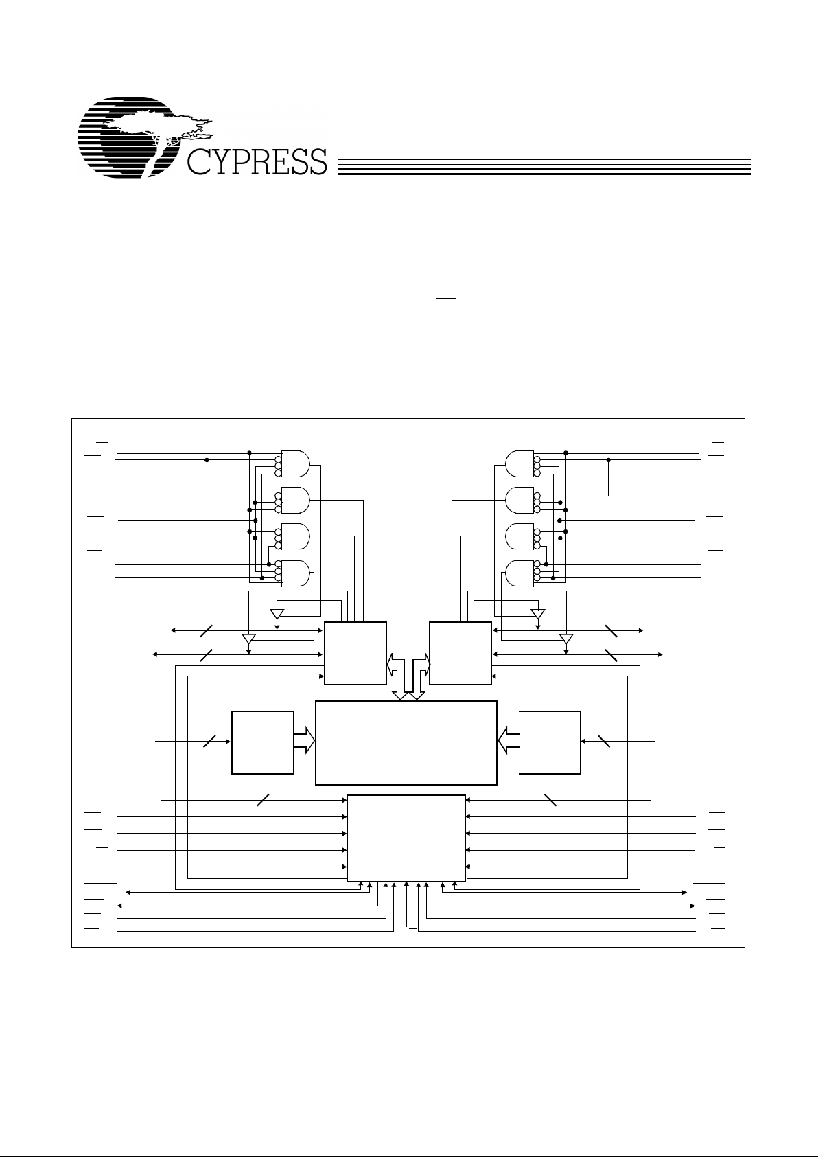
Logic Block Diagram
A0L–A
11/1213L
True Dual-Ported
RAM Array
A0R–A
11/12/13R
CE
R
OE
R
R/W
R
BUSY
R
SEM
R
INT
R
UB
R
LB
R
Address
Decode
A
0R–A11/12/13R
[2]
[2]
[3]
[3]
[5]
[5]
12/13/14
8/9
8/9
12/13/14
8/9
8/9
12/13/14 12/13/14
[4]
[4]
[4]
[4]
For the most recent information, visi t th e Cypress web site at www .cypress.com
Page 2
CY7C024AV/025AV/026AV
CY7C0241AV/0251AV/036AV
2
PRELIMINARY
Functional Description
The CY7C024AV/025AV/026AV and CY7C0241AV/0251AV /
036AV are low-power CMOS 4K, 8K, and 16K x16/18 dualport static RAMs. Various arbitration schem es are incl uded o n
the devices to handle si tuations when multiple processors access the same piece of data. Two ports are provided, permitting independent, asynchronous access for reads and writes
to any location in memory. The devices can be utilized as standalone 16/18 -bit dual- port sta tic RAMs or m ult iple d e vices ca n
be combined in order to function as a 32/36-bit or wider master/slave dual-port static RAM. An M/S
pin is provided for implementing 32/ 36-bit or wi der memory applicati ons without th e
need for separate master and slave devices or additional discrete logic. Appl ication areas include in terprocessor/multiprocessor designs, communications status buffering, and dualport video/graphics memory .
Each port has independent control pins: Chip Enable (CE
),
Read or Write Enable (R/W
), and Output Enable (OE). Two
flags are provided on each port (BUSY
and INT). BUSY signals that the port is trying to access t he same location cur rently
being accessed by t he other port. The Int errupt fla g (INT
) permits communicati on between ports or systems by means of a
mail box. The semaphores are used to pass a flag, or token,
from one port to the other to indica te that a shar ed r esource i s
in use. The semaphore logic is comprised of eight shared
latches. Only one side can control the latch (semaphore) at
any time. Control of a semaphore indicates that a shared resource is in use. An automatic power-down feature is controlled independently on each port by a Chip Select (CE
) pin.
The CY7C024AV/025AV/026AV and CY7C0241AV/0251AV/
036AV are available in 100-pin Thin Quad Plastic Flatpacks
(TQFP).
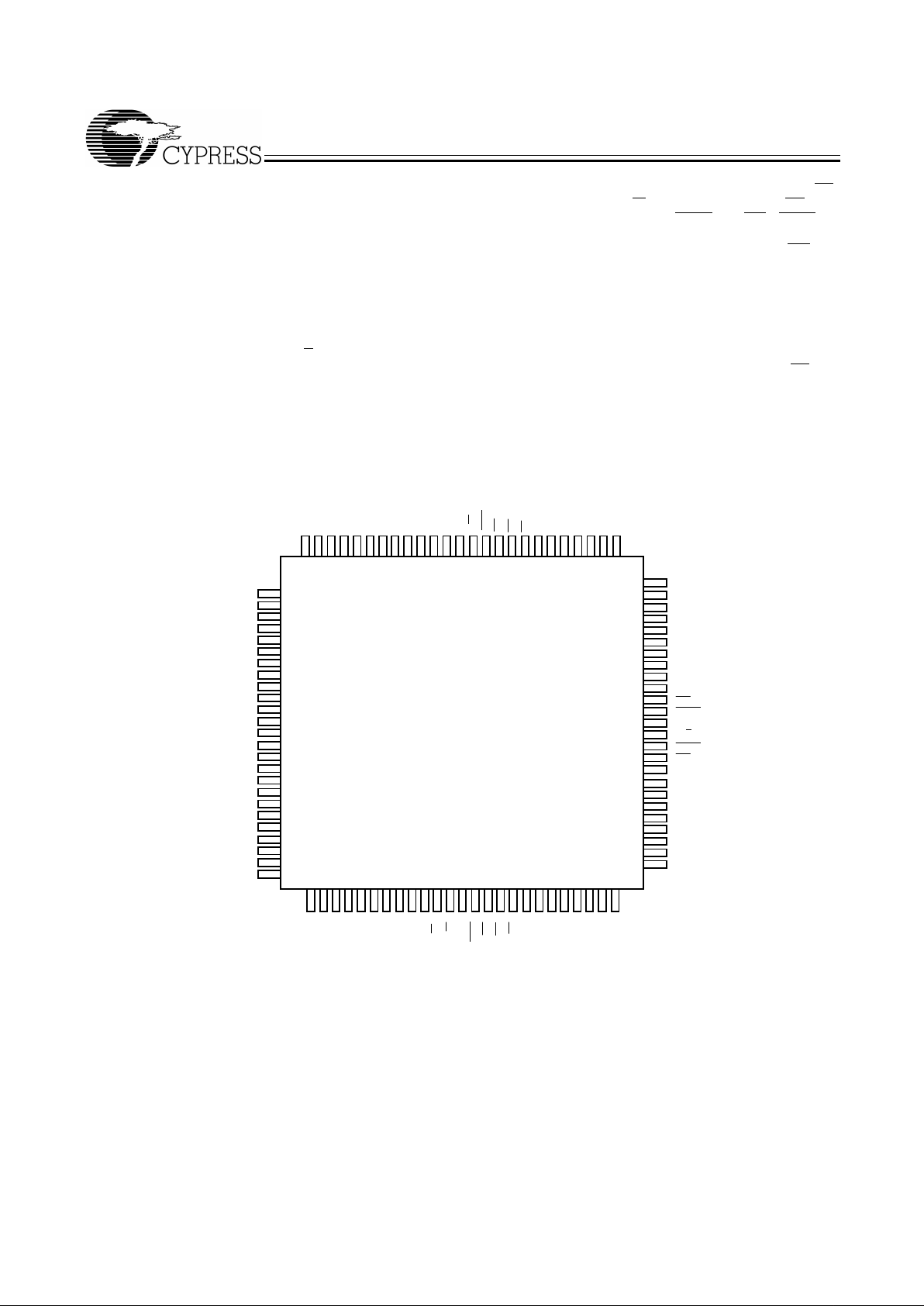
Pin Configurations
Notes:
6. A
12L
on the CY7C025AV.
7. A
12R
on the CY7C025AV.
Top Vie w
100-Pin TQFP
100 99 9798 96
2
3
1
4241
59
60
61
12
13
15
14
16
4
5
40
39
95 94
17
26
9
10
8
7
6
11
27 28 3029 31 32 3534 36 373833
67
66
64
65
63
62
68
69
70
75
73
74
72
71
89 88 8687 8593 92 84
NC
NC
NC
NC
A
5L
A
4L
INT
L
A
2L
A
0L
BUSY
L
GND
INT
R
A
0R
A
1L
NC
NC
NC
NC
I/O
10L
I/O
11L
I/O
15L
V
CC
GND
I/O
1R
I/O
2R
V
CC
9091
A
3L
M/S
BUSY
R
I/O
14L
GND
I/O
12L
I/O
13L
A
1R
A
2R
A
3R
A
4R
NC
NC
NC
NC
I/O
3R
I/O
4R
I/O
5R
I/O
6R
NC
NC
NC
NC
18
19
20
21
22
23
24
25
83 82 81 80 79 78 77 76
58
57
56
55
54
53
52
51
43 44 45 46 4748 49 50
I/O9LI/O8LI/O7LI/O6LI/O5LI/O4LI/O3LI/O
2L
GND
I/O1LI/O
0L
OE
L
SEM
L
V
CC
CE
L
UBLLBLNC
A
11LA10L
A9LA8LA7LA
6L
I/O
0R
I/O7RI/O8RI/O
9R
I/O
10R
I/O
11R
I/O
12R
I/O
13R
I/O
14R
GND
I/O
15R
Œ
R
R/W
R
GND
SEM
RCERUBRLBR
NC
A
11RA10R
A9RA8RA7RA6RA
5R
CY7C024AV (4K x 16)
R/W
L
[6]
[7]
CY7C025AV (8K x 16)
Page 3
CY7C024AV/025AV/026AV
CY7C0241AV/0251AV/036AV
3
PRELIMINARY
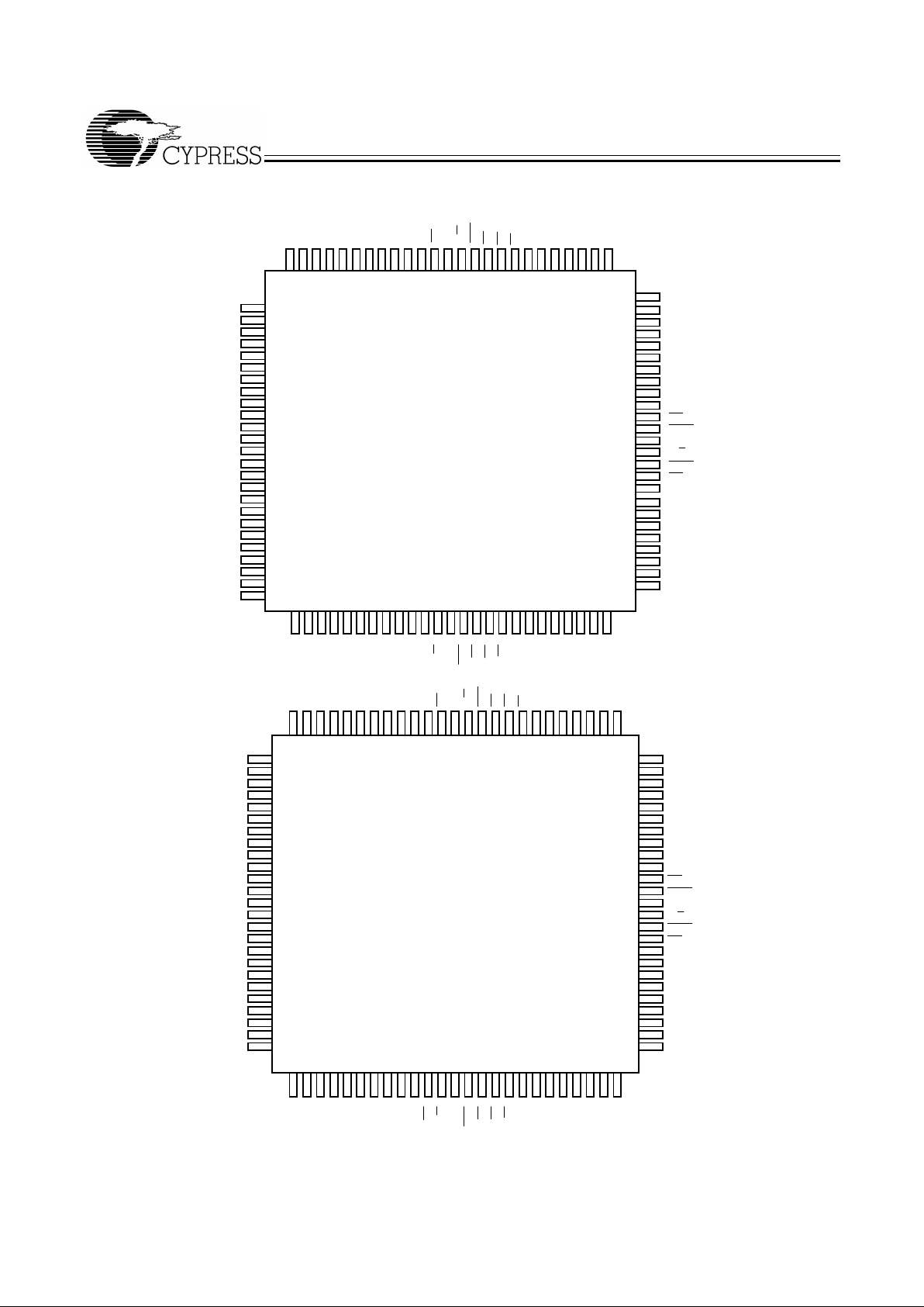
Pin Configurations
(continued)
Notes:
8. A
12L
on the CY7C0251AV.
9. A
12R
on the CY7C0251AVC.
T op View
100- Pin TQFP
100 99 9798 96
2
3
1
4241
59
60
61
12
13
15
14
16
4
5
4039
95 94
17
26
9
10
8
7
6
11
27 28 3029 31 32 3534 36 37 3833
67
66
64
65
63
62
68
69
70
75
73
74
72
71
89 88 8687 8593 92 84
NC
NC
NC
NC
A
5L
A
4L
INT
L
A
2L
A
0L
BUSY
L
GND
INT
R
A
0R
A
1L
NC
NC
I/O
11L
I/O
12L
I/O
16L
V
CC
GND
I/O
1R
I/O
2R
V
CC
9091
A
3L
M/S
BUSY
R
I/O
15L
GND
I/O
13L
I/O
14L
A
1R
A
2R
A
3R
A
4R
NC
NC
NC
NC
I/O
3R
I/O
4R
I/O
5R
I/O
6R
NC
NC
18
19
20
21
22
23
24
25
83 82 81 80 79 78 77 76
58
57
56
55
54
53
52
51
43 44 45 46 4748 49 50
I/O9LI/O7LI/O6LI/O5LI/O4LI/O3LI/O
2L
I/O
10L
GND
I/O1LI/O
0L
OE
L
SEM
L
V
CC
CE
L
UBLLB
L
NC
A
11LA10L
A9LA8LA7LA
6L
I/O
0R
I/O
7R
I/O
16R
I/O
9R
I/O
10R
I/O
11R
I/O
12R
I/O
13R
I/O
14R
GND
I/O
15R
OE
R
R/W
R
GND
SEM
RCERUBRLBR
NC
A
11RA10R
A9RA8RA7RA6RA
5R
CY7C0241AV (4K x 18)
I/O
8L
I/O
17L
I/O
8R
I/O
17R
R/W
L
[9]
[8]
1
3
2
92 91 90 848587 868889 83 82 81 7678 77798093949596979899100
59
60
61
67
66
64
65
63
62
68
69
70
75
73
74
72
71
NC
NC
NC
A6L
A5L
A4L
INT
L
A2L
A0L
GND
M/S
A0R
A1R
A1L
A3L
BUSYR
INTR
A2R
A3R
A4R
A5R
NC
NC
NC
BUSYL
58
57
56
55
54
53
52
51
CY7C026AV (16K x 16)
NC
NC
NC
NC
I/O10L
I/O11L
I/O15L
I/O13L
I/O14L
GND
I/O0R
VCC
I/O3R
GND
I/O12L
I/O1R
I/O2R
I/O4R
I/O5R
I/O6R
NC
NC
NC
NC
VCC
17
16
15
9
10
12
11
13
14
8
7
6
4
5
18
19
20
21
22
23
24
25
I/O9L
I/O8L
I/O7L
I/O6L
I/O5L
I/O4L
I/O0L
I/O2L
I/O1L
VCC
R/WL
UBL
LBL
GND
I/O3L
SEML
CEL
A113L
A12L
A11L
A10L
A9L
A8L
A7L
OEL
34 35 36 424139 403837 43 44 45 5048 494746
A6R
A7R
A8R
A9R
A10R
A11R
CER
A13R
UBR
GND
R/WR
GND
I/O14R
LBR
A12R
OER
I/O15R
I/O13R
I/O12R
I/O11R
I/O10R
I/O9R
I/O8R
I/O7R
SEMR
3332313029282726
CY7C0251 AV (8K x 18)
Page 4
CY7C024AV/025AV/026AV
CY7C0241AV/0251AV/036AV
4
PRELIMINARY
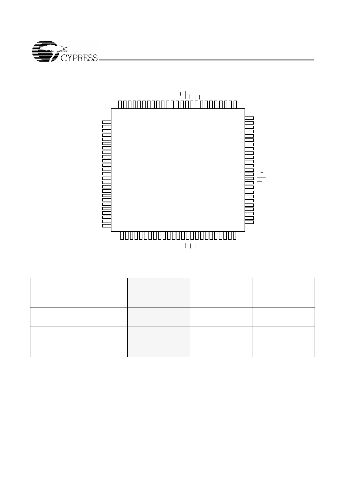
Pin Configurations
(continued)
Selection G uide
CY7C024AV/025AV/
026AV
CY7C0241AV/0251AV/
036AV
-15
[1]
CY7C024AV/025AV/
026AV
CY7C0241AV/0251AV/
036AV
-20
CY7C024AV/025AV/
026AV
CY7C0241AV/0251AV/
036AV
-25
Maximum Access Time (ns) 15 20 25
Typical Operat ing Current (mA) 125 120 115
Typical Standby Current for I
SB1
(mA)
(Both ports TTL Level)
35 35 30
Typical Standby Current for I
SB3
(µA)
(Both ports CMOS Level)
10 µA 10 µA 10 µA
Shaded areas contain advance information.
T op View
100-Pin TQFP
100 99 9798 96
2
3
1
4241
59
60
61
12
13
15
14
16
4
5
4039
95 94
17
26
9
10
8
7
6
11
27 28 3029 31 32 3534 36 37 3833
67
66
64
65
63
62
68
69
70
75
73
74
72
71
89 88 8687 8593 92 84
NC
NC
NC
A
5L
A
4L
INT
L
A
2L
A
0L
BUSY
L
GND
INT
R
A
0R
A
1L
NC
NC
I/O
11L
I/O
12L
I/O
16L
V
CC
GND
I/O
1R
I/O
2R
V
CC
9091
A
3L
M/S
BUSY
R
I/O
15L
GND
I/O
13L
I/O
14L
A
1R
A
2R
A
3R
A
4R
NC
NC
NC
I/O
3R
I/O
4R
I/O
5R
I/O
6R
NC
NC
18
19
20
21
22
23
24
25
83 82 81 80 79 78 77 76
58
57
56
55
54
53
52
51
43 44 45 46 47 48 49 50
I/O9LI/O7LI/O6LI/O5LI/O4LI/O3LI/O
2L
I/O
10L
GND
I/O1LI/O
0L
OE
L
SEM
L
V
CC
CE
L
UBLLB
L
A
11LA10L
A9LA8LA7LA
6L
I/O
0R
I/O
7R
I/O
16R
I/O
9R
I/O
10R
I/O
11R
I/O
12R
I/O
13R
I/O
14R
GND
I/O
15R
OE
R
R/W
R
GND
SEM
RCERUBRLBR
A
11RA10R
A9RA8RA7RA6RA
5R
I/O
8L
I/O
17L
I/O
8R
I/O
17R
R/W
L
CY7C036AV (16K x 18)
A
13L
A
13R
A
12L
A
12R
Page 5
CY7C024AV/025AV/026AV
CY7C0241AV/0251AV/036AV
5
PRELIMINARY
Maximum Ratings
(Above which the useful lif e may be impaired. For user guidelines, not tested.)
Storage Temperature ........................ .........–65
°
C to +150°C
Ambient Temperature with
Power Applied.............................................–55
°
C to +125°C
Supply Voltage to Ground Potential...............–0.5V to +4.6V
DC V oltage Applied to
Outputs in High Z State ...........................–0.5V to V
CC
+0.5V
DC Input Voltage
[10]
.................................–0.5V to VCC+0.5V
Output Current into Outputs (LOW)............................. 20 mA
Static Discharge Voltage ........... .............. .. ............. .. >2001V
Latch-Up Current............. .. .............. ........... ............ >200 mA
Notes:
10. Pulse width < 20 ns.
11. Industrial parts are available in CY7C026AV and CY7C036AV only .
Pin Definitions
Left Port Right Por t Description
CE
L
CE
R
Chip Enable
R/W
L
R/W
R
Read/Write Enable
OE
L
OE
R
Output Enable
A0L–A
13L
A0R–A
13R
Address (A0–A11 for 4K devices; A0–A12 for 8K devices; A0–A13 for 16K)
I/O0L–I/O
17L
I/O0R–I/O
17R
Data Bus Input/Output
SEML SEM
R
Semaphore Enable
UB
L
UB
R
Upper Byte Select ( I/O8–I/O15 for x1 6 de v ices; I/O9–I/O17 for x 18 devices)
LB
L
LB
R
Lower Byte Select (I/O0–I/O7 for x16 devices; I/O0–I/O8 for x18 devices)
INT
L
INT
R
Interrupt Flag
BUSY
L
BUSY
R
Busy Flag
M/S Master or Slave Select
V
CC
Power
GND Ground
NC No Connect
Operating Range
Range
Ambient
Temperature
V
CC
Commercial 0°C to +70°C 3.3V ± 300 mV
Industrial
[11]
–40°C to +85°C 3.3V ± 300 mV
Shaded areas contain advance information.
Page 6

CY7C024AV/025AV/026AV
CY7C0241AV/0251AV/036AV
6
PRELIMINARY
Notes:
12. f
MAX
= 1/tRC = All inputs c ycling at f = 1/tRC (except output enab le) . f = 0 mea ns no add ress or control lines change . T his appl ies onl y to inpu ts at CM OS level standby I
SB3
.
13. Tested initially and after any design or process changes that may affect these parameters.
Electrical Characteristics
Over the Operating Range
Parameter Description
CY7C024AV/025AV/026AV
CY7C0241AV/0251AV/036AV
Unit
-15
[1]
-20 -25
Min. Typ. Max. Min. Typ. Max. Mi n. Typ. Max.
V
OH
Output HIGH Voltage (VCC=3.3V) 2.4 2.4 2.4 V
V
OL
Output LO W Voltage 0.4 0.4 0.4 V
V
IH
Input HIGH Voltage 2.0 2.0 2.0 V
V
IL
Input LOW Voltage 0.8 0.8 0.8 V
I
OZ
Output Leakage Curr ent –10 10 –10 10 –10 10 µA
I
IX
Input Leakage Current –10 10 –10 10 –10 10 µA
I
CC
Operating Cur rent (V
CC
= Max.,
I
OUT
= 0 mA) Outputs Disabled
Com’l.
125 185 120 175 115 165 mA
Ind.
[11]
135 185 mA
I
SB1
Standby Current (Both Por ts TTL
Level) CE
L
& CER ≥ VIH, f = f
MAX
Com’l. 35 50 35 45 30 40 mA
Ind.
[11]
40 50 mA
I
SB2
Standby Current (One Port TTL
Level) CE
L
| CER ≥ VIH, f = f
MAX
Com’l. 80 120 75 110 65 95 mA
Ind.
[11]
75 105 mA
I
SB3
Standby Curre nt (Both Ports CMOS
Level) CE
L
& CER ≥ V
CC
−0.2V , f = 0
Com’l.
10 500 10 500 10 500 µA
Ind.
[11]
10 500
µA
I
SB4
Standby Current (One Port CMOS
Level) CE
L
| CER ≥ VIH, f = f
MAX
[12]
Com’l. 75 105 70 95 60 80 mA
Ind.
[11]
70 90 mA
Shaded areas contain advance information.
Capacitance
[13]
Parameter Description Test Conditions Max. Unit
C
IN
Input Capacitance TA = 25°C, f = 1 MHz,
V
CC
= 3.3V
10 pF
C
OUT
Output Capacitance 10 pF
AC Test Loads and Waveforms
3.0V
GND
90%
90%
10%
3ns
3
ns
10%
ALL INPUTPULSES
(a) Normal Load (Load
1)
R1= 590
Ω
3.3V
OUTPUT
R2= 435
Ω
C= 30
pF
V
TH
=1.4V
OUTPUT
C=
30pF
(b) Thévenin Equivalent (Load 1)
(c)Three-State Delay(Load2)
R1= 590
Ω
R2= 435
Ω
3.3V
OUTPUT
C= 5pF
R
TH
=250
Ω
≤
≤
including scope and jig)
(Used for t
LZ
, tHZ, t
HZWE
, & t
LZWE
Page 7

CY7C024AV/025AV/026AV
CY7C0241AV/0251AV/036AV
7
PRELIMINARY
Switching Characteristics
Over the Operating Range
[14]
Parameter Description
CY7C024AV/025AV/026AV
CY7C0241AV/0251AV/036AV
Unit
-15
[1]
-20 -25
Min. Max. Min. Max. Mi n. Max.
READ CYCLE
t
RC
Read Cycle Time 15 20 25 ns
t
AA
Address to Data Valid 15 20 25 ns
t
OHA
Output Hold From Address Change 3 3 3 ns
t
ACE
[15]
CE LOW to Data Valid 15 20 25 ns
t
DOE
OE LOW to Data Valid 10 12 13 ns
t
LZOE
[16, 17, 18]
OE Low to Low Z 3 3 3 ns
t
HZOE
[16, 17, 18]
OE HIGH to High Z 10 12 15 ns
t
LZCE
[16, 17, 18]
CE LOW to Low Z 3 3 3 ns
t
HZCE
[16, 17 , 18]
CE HIGH to High Z 10 12 15 ns
t
PU
[18]
CE LOW to Po wer-Up 0 0 0 ns
t
PD
[18]
CE HIGH to Power-Down 15 20 25 ns
t
ABE
[15]
Byte Enable Access Time 15 20 25 ns
WRITE CYCLE
t
WC
Wr ite Cyc l e Time 15 20 25 ns
t
SCE
[15]
CE LOW to Write End 12 15 20 ns
t
AW
Address V alid to Write End 12 15 20 ns
t
HA
Address Hold From Write End 0 0 0 ns
t
SA
[15]
Address Set-Up to Write Start 0 0 0 ns
t
PWE
Writ e Pu ls e Wid t h 12 15 20 ns
t
SD
Data Se t- U p to Wr ite End 10 15 15 ns
t
HD
Data Hold From Write End 0 0 0 ns
t
HZWE
[17, 18]
R/W LO W to High Z 10 12 15 ns
t
LZWE
[17, 18]
R/W HIGH to Low Z 3 3 0 ns
t
WDD
[19]
Writ e Pu ls e to Dat a De lay 30 45 50 ns
t
DDD
[19]
Write Data Valid to Read Data Valid 25 30 35 ns
Notes:
14. Tes t conditions assume signal transition time of 3 ns or less, timing reference levels of 1.5V, input pulse levels of 0 to 3.0V, and output loading of the specified
I
OI/IOH
and 30-pF load ca pacitance.
15. To access RAM, CE
=L, UB=L, SEM= H. To access semaphore, C E=H and SEM=L. Either condi tion mu st be v al id f or the enti re t
SCE
time.
16. At any given temperature and voltage condition for any given device, t
HZCE
is less than t
LZCE
and t
HZOE
is less than t
LZOE
.
17. Test conditions used are Load 3.
18. This parameter is guaranteed but not tested. For information on port-to-port delay through RAM cells from writing port to reading port, refer to Read Timing
with Busy waveform.
19. For information on port-to-port delay through RAM cells from writing port to reading port, refer to Read Timing with Busy waveform.
Page 8

CY7C024AV/025AV/026AV
CY7C0241AV/0251AV/036AV
8
PRELIMINARY
Data Retention Mode
The CY7C024AV/025AV/026AV and CY7C0241AV/0251AV/
036AV are designed with battery backup in mind. Data retention vol tage and supply curren t are guaranteed over temperature. The following rules ensure data retention:
1. Chip Enable (C E
) must be held HIGH during data retention, with-
in V
CC
to VCC – 0.2V .
2. CE
must be kept between VCC – 0.2V and 70% of VCC
during the power-up and power-down transitions.
3. The RAM can begin operati on >t
RC
after VCC reaches the
minimum operating voltage (3.0 volts).
Notes:
20. Test conditions used are Load 2.
21. t
BDD
is a calculate d paramet er and is the gr eater of t
WDD–tPWE
(actual) or t
DDD–tSD
(actual).
22. CE
= VCC, Vin = GND to VCC, TA = 25°C. This paramet er is guar anteed but not tested.
BUSY TIMING
[20]
t
BLA
BUSY LOW from Addr ess M atch 15 20 20 ns
t
BHA
BUSY HIGH from Address Mismatch 15 20 20 ns
t
BLC
BUSY LOW from CE LOW 15 20 20 ns
t
BHC
BUSY HIGH from CE HIGH 15 17 17 ns
t
PS
Port Set-Up for Priority 5 5 5 ns
t
WB
R/W HIGH after BUSY (Slave) 0 0 0 ns
t
WH
R/W HIGH after BUSY HIGH (Slave) 13 15 17 ns
t
BDD
[21]
BUSY HIGH to Data Valid 15 20 25 ns
INTERRUPT TIMING
[20]
t
INS
INT Set Time 15 20 20 ns
t
INR
INT Reset Time 15 20 20 ns
SEMAPHORE TIMING
t
SOP
SEM Flag Update Pulse (OE or SEM) 10 10 12 ns
t
SWRD
SEM Flag Write to Read Time 5 5 5 ns
t
SPS
SEM Flag Contention Window 5 5 5 ns
t
SAA
SEM Address Access Time 15 20 25 ns
Switching Characteristics
Over the Operating Range
[14]
(continued)
Parameter Description
CY7C024AV/025AV/026AV
CY7C0241AV/0251AV/036AV
Unit
-15
[1]
-20 -25
Min. Max. Min. Max. Mi n. Max.
Timing
Parameter Test Conditions
[22]
Max. Unit
ICC
DR1
@ VCCDR = 2V 50
µA
Data Rete ntion Mode
3.0V
3.0V
V
CC
>
2.0V
V
CC
to VCC– 0.2V
V
CC
CE
t
RC
V
IH
Page 9

CY7C024AV/025AV/026AV
CY7C0241AV/0251AV/036AV
9
PRELIMINARY
Switching Waveforms
Notes:
23. R/W
is HIGH for read cycles.
24. Device is continuously selected CE = VIL and UB or LB = VIL. This wav ef orm cannot be used f or semaphore r eads.
25. OE
= VIL.
26. Address valid prior to or coincident with CE
transition LO W.
27. To access RAM, CE = VIL, UB or LB = VIL, SEM = VIH. T o ac cess semaphor e, CE = VIH, SEM = VIL.
t
RC
t
AA
t
OHA
DATA VALIDPREVIOUS DATA VALID
DATA O UT
ADDRESS
t
OHA
Read Cycle No.1 (Eithe r Port Address Access )
[23, 24, 25]
t
ACE
t
LZOE
t
DOE
t
HZOE
t
HZCE
DAT A VALID
t
LZCE
t
PU
t
PD
I
SB
I
CC
DATA OU T
OE
CE and
LB
or UB
CURRENT
Read Cycle No.2 (Either Port CE/OE Access)
[23, 26, 27]
UB or LB
DAT A OUT
t
RC
ADDRESS
t
AA
t
OHA
CE
t
LZCE
t
ABE
t
HZCE
t
HZCE
t
ACE
t
LZCE
Read Cycle No. 3 (Either Port)
[23, 25, 26, 27]
Page 10

CY7C024AV/025AV/026AV
CY7C0241AV/0251AV/036AV
10
PRELIMINARY
Notes:
28. R/W
must be HIGH dur ing all address trans itions .
29. A write occurs during the overlap (t
SCE
or t
PWE
) of a LO W CE or SEM and a LO W UB or LB.
30. t
HA
is measured from the ea rlier of CE or R /W or (SEM or R/W) going HIGH at the end of write c ycle .
31. If OE
is LOW during a R/W controll ed write cycle, the write pulse widt h must be the larger of t
PWE
or (t
HZWE
+ tSD) to allow the I/O driver s to turn off and data to be placed on
the bus f or the requ ired t
SD
. If OE is HI GH during an R/W contro lled write cycl e, this re quireme nt does n ot app ly and the write p ulse can be as s hort as t he speci fied t
PWE
.
32. To access RAM, CE
= VIL, SEM = VIH.
33. To access upper byte, CE
= VIL, UB = VIL, SEM = VIH.
To a ccess lower b y t e, CE
= VIL, LB = VIL, SEM = VIH.
34. Transition is measured ±500 mV from steady s tate with a 5-pF loa d (incl uding scope and jig) . Thi s parameter is sampled a nd not 100% tested.
35. During this period, the I/O pins are in the output state, and input signals must not be applied.
36. If the CE
or SEM LOW transi tion occ urs simu ltaneous ly with o r after the R/W LO W tr ansi tion, the out puts r emain in t he high- impedanc e state.
Switching Waveforms
(continued )
t
AW
t
WC
t
PWE
t
HD
t
SD
t
HA
CE
R/W
OE
DA TA OUT
DATA I N
ADDRESS
t
HZOE
t
SA
t
HZWE
t
LZWE
Write Cycl e No.1: R/W Controlled Timing
[28, 29, 30, 31]
[34]
[34]
[31]
[32,33]
NOTE 35
NOTE 35
t
AW
t
WC
t
SCE
t
HD
t
SD
t
HA
CE
R/W
DATA I N
ADDRESS
t
SA
Write Cycle No. 2: CE Controlled Timing
[28, 29, 30, 36]
[32,33]
Page 11

CY7C024AV/025AV/026AV
CY7C0241AV/0251AV/036AV
11
PRELIMINARY
Notes:
37. CE
= HIGH for the duration of the above timing (both write and read cycle).
38. I/O0R = I/O0L = LOW (reques t semaph ore); CER = CEL = HIGH.
39. Semaphores are reset (available to both ports) at cycle start.
40. If t
SPS
is violated, the s emaphore w ill de fini tely be obt ained b y one side or the ot her , b ut whic h side will get the semaphore is unpredictable .
Switching Waveforms
(continued )
t
SOP
t
SAA
VALID ADRESS VALID ADRESS
t
HD
DAT AINVALID
DA TA
OUT
VALID
t
OHA
t
AW
t
HA
t
ACE
t
SOP
t
SCE
t
SD
t
SA
t
PWE
t
SWRD
t
DOE
WRITE CYCLE READ CYCLE
OE
R/W
I/O
0
SEM
A0–A
2
Semaphore Read After Write Timing, Either Side
[37]
MATCH
t
SPS
A0L–A
2L
MATCH
R/W
L
SEM
L
A0R–A
2R
R/W
R
SEM
R
Timing Diagram of Semaphore Contenti on
[38, 39, 40 ]
Page 12

CY7C024AV/025AV/026AV
CY7C0241AV/0251AV/036AV
12
PRELIMINARY
Note:
41. CE
L
= CER = LOW.
Switching Waveforms
(continued )
VALID
t
DDD
t
WDD
MATCH
MATCH
R/W
R
DATA I N
R
DAT A
OUTL
t
WC
ADDRESS
R
t
PWE
VALID
t
SD
t
HD
ADDRESS
L
t
PS
t
BLA
t
BHA
t
BDD
BUSY
L
Timing Diagram of Read with BUSY (M/S=HIGH)
[41]
t
PWE
R/W
BUSY
t
WB
t
WH
Write Timing with Busy Input (M/S=LOW)
Page 13

CY7C024AV/025AV/026AV
CY7C0241AV/0251AV/036AV
13
PRELIMINARY
Note:
42. If t
PS
is violated, the b us y s ignal will be asserted on one side or the other, but there is no guarantee t o which si de BU SY will be asserted.
Switching Waveforms
(continued )
ADDRESS MATCH
t
PS
t
BLC
t
BHC
ADDRESS MATCH
t
PS
t
BLC
t
BHC
CERValidFirst:
ADDRESS
L,R
BUSY
R
CE
L
CE
R
BUSY
L
CE
R
CE
L
ADDRESS
L,R
Busy Timing Diagram No.1 (CE Arbitration)
[42]
CELVal id Fi rs t :
ADDRESS MATCH
t
PS
ADDRESS
L
BUSY
R
ADDRESS MISMATCH
t
RC
or t
WC
t
BLA
t
BHA
ADDRESS
R
ADDRESS MATCH ADDRESS MISMA TCH
t
PS
ADDRESS
L
BUSY
L
tRCor t
WC
t
BLA
t
BHA
ADDRESS
R
Right Address Valid First:
Busy Timing Diagram No.2 (Address Arbitration)
[42]
Left Address Valid First:
Page 14

CY7C024AV/025AV/026AV
CY7C0241AV/0251AV/036AV
14
PRELIMINARY
Notes:
43. t
HA
depends on which enab le pin ( CEL or R/WL) is deasserted first.
44. t
INS
or t
INR
depends on which ena ble p in (CEL or R/WL) is asserted last.
Switching Waveforms
(continued )
Interrupt Timing Diagrams
WRITE 1FFF (OR 1/3FFF)
t
WC
Right SideClears INTR:
t
HA
READ 7FFF
t
RC
t
INR
WRITE 1FFE (OR 1/3FFE)
t
WC
Right SideSetsINT
L
:
Left Side Set s INT
R
:
Left SideClears INT
L
:
READ 7FFE
t
INR
t
RC
ADDRESS
R
CE
L
R/W
L
INT
L
OE
L
ADDRESS
R
R/W
R
CE
R
INT
L
ADDRESS
R
CE
R
R/W
R
INT
R
OE
R
ADDRESS
L
R/W
L
CE
L
INT
R
t
INS
t
HA
t
INS
(OR 1/3FFF)
OR 1/3FFE)
[43]
[44]
[44]
[44]
[43]
[44]
Page 15

CY7C024AV/025AV/026AV
CY7C0241AV/0251AV/036AV
15
PRELIMINARY
Architecture
The CY7C024AV/025AV/026AV and CY7C0241AV/0251AV/
036AV consi st of an arr ay of 4K, 8K, and 16K w ords of 16 and
18 bits eac h of dua l-p ort RAM cel ls , I/ O an d addr es s li ne s, and
control sign al s (CE
, OE, R/W). These control pins permit independent access for reads or writes to any location in memory.
To handle simultaneous writes/reads to the same location, a
BUSY
pin is prov ided on eac h port. T wo Int errupt (INT) pins can
be utilized for port-to-port communication. Two Semaphore
(SEM
) control pins are used for allocating shared resources.
With the M/S
pin, the devices can function as a mas ter (BUSY
pins a re ou tputs) or as a slave (BU SY pins are inputs). The
dev ices also ha v e an au t omat ic p o wer- do wn fe at ure c ontr ol led
by CE
. Each port is provided with its own output enable control
(OE
), which allows data to be read from the device.
Functional Description
Write Operation
Data must be set up for a duration of t
SD
before the rising edge
of R/W
in order to gu arant ee a valid w rite. A w rite opera tion is
controlled by either the R/W
pin (see Wr ite Cycle N o. 1 wave-
form) or the CE
pin (see Write Cycle No . 2 w av ef orm). Requi red
inputs for non-contention operations are summarized in T able 1.
If a location is being written to by one port and the opposite
port attempts to read that location, a port-to-port flowthrough
delay m ust occur before t he data is read on the output; othe rwise the data read is not det erministic. Data will be v alid on the
port t
DDD
after the data is presented on the other port.
Read Operation
When reading the device, the user must assert both the OE
and CE pins. Dat a will be available t
ACE
after CE or t
DOE
after
OE
is asserted. If the user wi shes to acces s a semaphore flag,
then the SEM
pin must be asserted instea d of the CE pi n, and
OE
must also be asserted.
Interrupts
The upper two memory locations may be used for message
passing. The highest memory location (FFF for the
CY7C024AV/41AV, 1FFF for the CY7C025AV/51AV, 3FFF for
the CY7C026A V/36AV) is the mailbox for the righ t port and the
second-highest memory location (FFE for the CY7C024AV/
41AV, 1FFE for the CY7C025AV/51AV, 3FFE for the
CY7C026AV/36AV) is the mailbox for the left port. When one
port writes to the other port’s mailbo x, an interrupt is gener ated
to the owner. The interrupt is reset when the owner reads the
contents of the mailbox. The message is user defined.
Each port can read the other port’s mailbox without resetting
the interrupt. The active state of the busy signal (to a port)
preve nts the port from setti ng the in terrupt to the winni ng port.
Also, an active busy to a por t prevents that port from reading
its own mailbox and, thus, resetting the interrupt to it.
If an application does not require message passing, do not connect the interrupt pin to the processor’s interrupt request input pin.
The operation of the interrupts and their interaction with Busy
are summarized in Table 2.
Busy
The CY7C024AV/025AV/026AV and CY7C0241AV/0251AV/
036AV provide on-chip arbitration to resolve simultaneous
memory location access (contention). If both ports’ CE
s are
asserted and an address match occurs within t
PS
of each oth-
er, the busy logic will determine which port has access. If t
PS
is violated, one port will definitely gain permission to the loca tion, but it is not predict able whic h port will get that permiss ion.
BUSY
will be asserted t
BLA
after an address match or t
BLC
after CE is taken LOW.
Master/Slave
A M/S
pin is provided in order to expand the word width by
configuring the d evice as either a master or a slav e. The BUSY
output of the master is connected to the BUSY input of the
slave . This wil l allo w the de vice to interface to a master device
with no external componen ts. Writi ng to slav e devi ces must be
delayed until after the BUSY
input has settled (t
BLC
or t
BLA
),
otherwise, the slav e chip ma y begin a writ e cycle during a con tention situation. When tied HIGH, the M/S
pin allows the de-
vice to be used as a master and, therefore, the BUSY
line is
an output. BUSY
can then be used to send the arbitr ati on out-
come to a slave.
Semaphore Operation
The CY7C024AV/025AV/026AV and CY7C0241AV/0251AV/
036AV provide eight semaphore latches, which are separate
from the dual-port memory loc ations. Sem aphores are used to
reserve resources t hat are share d between the two p orts. The
state of the semaphor e indic ates that a resourc e is in use . Fo r
example, if the left port wants to request a given resource, it
sets a latch b y writing a z ero to a semap hore location. The lef t
port then verifies its success in setting the latch by reading it.
After writing to the semaphore , SEM
or OE must be deassert-
ed for t
SOP
before attempting to read the semaphore. The
semaphore va lue will be available t
SWRD
+ t
DOE
after t he ri sing
edge of the semaphore write. If the left port was successful
(reads a zero) , it assum es contr ol of t he sha red reso urce, oth erwise (reads a one) it assumes the right port has cont rol and
continues to poll the semaphore. When the right side has relinquished contr ol of the semaphore (b y writi ng a one), the left
side will succee d in gaini ng control of the semaph ore. If the lef t
side no longer requires the semaphore, a one is written to
cancel its request.
Semaphores are accessed by asserting SEM
LOW. The SEM
pin functions as a chip select for the semaphore latches (CE
must remain HIGH during SEM LOW). A
0–2
represents the
semaphore address. OE
and R/W are used in the same manner as a normal memory access. When writing or reading a
semaphore, the other address pins have no effect.
When writing to the semaphore, only I/O
0
is used. If a zero is
written to the left port of an available semaphore, a one will
appear at the same semaphor e address on the right port. That
semaphore can now only be modifi ed by the side showing zero
(the left port in this case). If the lef t port now relinq uishes con trol by writing a one to the semaphore, the semaphore will be
set to one f or both sides. Howe ver , i f the right p ort had request ed the semaphore (written a zero) while the left port had control, the right port would immediately own the semaphore as
soon as the left port released it. Table 3 shows sample semaphore operatio ns.
When reading a semaphore, all sixteen/eighteen data lines
output the semaphore value. The read value is latched in an
output register t o prevent the semaphore from changing state
during a write from the other port. If both ports attempt to access the sem aphore within t
SPS
of each other, the semaphore
will defini tel y be obtained by one side or the othe r, but there is
no guarantee which side wil l control the semaphore.
Page 16

CY7C024AV/025AV/026AV
CY7C0241AV/0251AV/036AV
16
PRELIMINARY
Table 1. Non-Contending Read/Write
Inputs Outputs
CE R/W OE UB LB SEM I/O
9
–
I/O
17
I/O
0
–
I/O
8
Operation
H X X X X H High Z High Z Deselected: Power-Down
X X X H H H High Z High Z Deselected: Power-Down
L L X L H H Data In High Z Write to Upper Byte Only
L L X H L H High Z Data In Write to Lower B y te Only
L L X L L H Data In Data In Write to Both Bytes
L H L L H H Data Out High Z Read Upper Byte Only
L H L H L H High Z Data Out Read Lower Byte Only
L H L L L H Data Out Data Out Read Both Bytes
X X H X X X High Z High Z Outputs Disabled
H H L X X L Data Out Dat a Out Read Data in Semaphore Flag
X H L H H L Data Out Data Out Read Data in Semaphore Flag
H X X X L Data In Data In Write D
IN0
into Semaphore Flag
X X H H L Data In Data In Write D
IN0
into Semaphore Flag
L X X L X L Not Allowed
L X X X L L Not Allowed
T able 2. Interrupt Operation Example (assumes BUSY
L
=BUSYR=HIGH)
[45]
Left Port Right Port
Function R/WLCELOE
L
A
0L–13
L
INTLR/WRCEROE
R
A
0R–13R
INT
R
Set Right INTR Flag L L X FFF
[48]
X X X X X L
[47]
Reset Right INTR Flag X X X X X X L L FFF (or 1/3FFF) H
[46]
Set Left INTL Flag X X X X L
[46]
L L X 1FFE (or 1/
3FFE)
X
Reset Le f t INTL Flag X L L 1FFE
[48]
H
[47]
X X X X X
T able 3. Semaphore Operation Example
Function I/O
0
–
I/O
17
Left I/O
0
–
I/O
17
Right Status
No action 1 1 Semaphore free
Left port writes 0 to semaphore 0 1 Left Port has semaphore token
Right port writes 0 to semaphore 0 1 No change. Right side has no write access to semaphore
Left port writes 1 to semaphore 1 0 Right port obtains semaphore token
Left port writes 0 to semaphore 1 0 No change. Left port has no write access to semaphore
Right port writes 1 to semaphore 0 1 Left port obtains semaphore token
Left port writes 1 to semaphore 1 1 Semaphore free
Right port writes 0 to semaphore 1 0 Right port has semaphore tok en
Right port writes 1 to semaphore 1 1 Semaphore free
Left port writes 0 to semaphore 0 1 Left port has semaphore token
Left port writes 1 to semaphore 1 1 Semaphore free
Notes:
45. See Functional Description for specific highest memory locations by device.
46. If BUSY
R
=L, then no change .
47. If BUSY
L
=L, then no change .
48. See Functional Description for specific addresses by device.
Page 17

CY7C024AV/025AV/026AV
CY7C0241AV/0251AV/036AV
17
PRELIMINARY
Ordering Information
Document #: 38–00838
4K x16 3.3V Asynchronous Dual-Port SRAM
Speed
(ns) Ordering Code
Package
Name Pac kage Type
Operating
Range
15
[1]
CY7C024AV-15AC A100 100-Pin Thin Quad Flat Pack Commercial
20 CY7C024AV-20AC A100 100-Pin Thin Quad Flat Pack Commercial
25 CY7C024AV-25AC A100 100-Pin Thin Quad Flat Pack Commercial
8K x16 3.3V Asynchronous Dual-Port SRAM
Speed
(ns) Ordering Code
Package
Name Pac kage Type
Operating
Range
15
[1]
CY7C025AV-15AC A100 100-Pin Thin Quad Flat Pack Commercial
20 CY7C025AV-20AC A100 100-Pin Thin Quad Flat Pack Commercial
25 CY7C025AV-25AC A100 100-Pin Thin Quad Flat Pack Commercial
16K x18 3.3V Asynchronous Dual-Port SRAM
Speed
(ns)
Ordering Code
Package
Name
Pac kage Type
Operating
Range
15
[1]
CY7C026AV-15AC A100 100-Pin Thin Quad Flat Pack Commercial
20 CY7C026AV-20AC A100 100-Pin Thin Quad Flat Pack Commercial
25 CY7C026AV-25AC A100 100-Pin Thin Quad Flat Pack Commercial
CY7C026AV-25AI A100 100-Pin Thin Quad Flat Pack Industrial
4K x18 3.3V Asynchronous Dual-Port SRAM
Speed
(ns) Ordering Code
Package
Name Pac kage Type
Operating
Range
15
[1]
CY7C0241AV-15AC A100 100-Pin Thin Quad Flat Pack Commercial
20 CY7C0241AV-20AC A100 100-Pin Thin Quad Flat Pack Commercial
25 CY7C0241AV-25AC A100 100-Pin Thin Quad Flat Pack Commercial
8K x18 3.3V Asynchronous Dual-Port SRAM
Speed
(ns) Ordering Code
Package
Name Pac kage Type
Operating
Range
15
[1]
CY7C0251AV-15AC A100 100-Pin Thin Quad Flat Pack Commercial
20 CY7C0251AV-20AC A100 100-Pin Thin Quad Flat Pack Commercial
25 CY7C0251AV-25AC A100 100-Pin Thin Quad Flat Pack Commercial
16K x18 3.3V Asynchronous Dual-Port SRAM
Speed
(ns)
Ordering Code
Package
Name
Pac kage Type
Operating
Range
15
[1]
CY7C036AV-15AC A100 100-Pin Thin Quad Flat Pack Commercial
20 CY7C036AV-20AC A100 100-Pin Thin Quad Flat Pack Commercial
25 CY7C036AV-25AC A100 100-Pin Thin Quad Flat Pack Commercial
CY7C036AV-25AI A100 100-Pin Thin Quad Flat Pack Industrial
Shaded areas contain advance information.
Page 18

CY7C024AV/025AV/026AV
CY7C0241AV/0251AV/036AV
PRELIMINARY
© Cypress Semiconductor Corporation, 1999. The information contained herein is subject to change without notice. Cypress Semiconductor Corporation assumes no responsibility for the use
of any circuitry other than circuitry embodied in a Cypress Semiconductor product. Nor does it con vey or imply any license under patent or other rights. Cypress Semiconductor does not authorize
its products for use as critical components in life-support systems where a malfunction or failure may reasonably be expected to result in significant injury to the user. The inclusion of Cypress
Semiconductor products in life-support systems application implies that the manufacturer assumes all risk of such use and in doing so indemnifies Cypress Semiconductor against all charges.
Package Diagram
100-Pin Thin Plastic Quad Fl at Pack (T QF P) A100
51-85048-B
 Loading...