

Datasheet CY6264-70SNC, CY6264-70SC, CY6264-55SNC, CY6264-55SC Datasheet (Cypress Semiconductor)
Page 1
PRELIMINARY
8K x 8 Static RAM
CY6264
1CY6264
Features
over 70% when deselected. The CY6264 is packaged in a
450-mil (300-mil body) SOIC.
• 55, 70 ns access times
• CMOS for optimum speed/power
• Easy memory expansion with CE
tures
, CE2, and OE fea-
1
• TTL-compatible inputs and outputs
• Automatic power-down when deselected
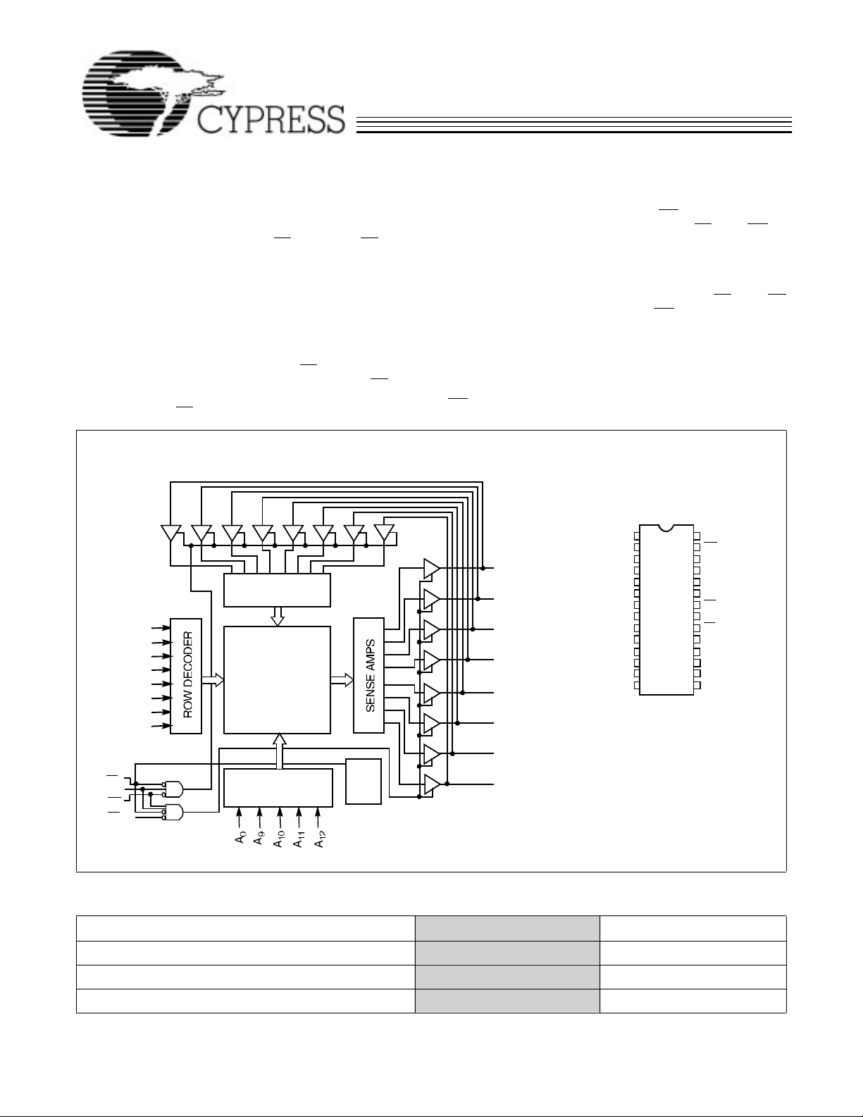
Functional Description
An active LOW write enable signal (WE
ing/reading operation of the memory. When CE
puts are both LOW and CE
input/output pins (I/O
location addressed by the address present on the address
pins (A
selecting the device and enabling the outputs, CE
through A12). Reading the device is accomplished by
0
0
is HIGH, data on the eight data
2
through I/O7) is written into the memory
active LOW, CE2 active HIGH, whil e WE remains inacti ve or
) controls the writ-
HIGH. Under these conditions, the contents of the location adThe CY6264 is a high-performance CMOS static RAM organized as 8192 words by 8 bits. Easy memory expansion is
provided by an active LOW chip enable (CE
chip enable (CE
three-state drivers. Both devices have an automatic power-down feature (CE
), and active LOW output enable (OE) and
2
), reducing the power consumption by
1
), an active HIGH
1
dressed by the information on address pins is present on the
eight data input/output pins.
The input/output pins remain in a high-impedance state unle ss
the chip is selected, outputs are enabled, and write enable
(WE
) is HIGH. A die coat is used to insure alpha immunity.
Logic Block Diagram Pin Configuration
SOIC
Top View
NC
1
A
4
2
A
5
3
A
6
A
A
A
I/O
I/O
I/O
GND
4
A
7
5
A
8
6
A
9
7
10
8
11
9
12
10
0
11
1
12
2
13
14
I/O
0
INPUT BUFFER
A
1
A
2
A
3
A
4
A
5
A
6
A
7
A
8
256 x 32 x 8
ARRAY
I/O
I/O
I/O
I/O
I/O
1
2
3
4
5
V
28
WE
27
CE
26
A
25
A
24
A
23
OE
22
A
21
CE
20
I/O
19
I/O
18
I/O
17
I/O
16
I/O
15
and WE in-
1
and OE
1
CC
2
3
2
1
0
1
7
6
5
4
3
CY6264-2
I/O
6
CE
CE
WE
OE
1
2
COLUMN DECODER
POWER
DOWN
I/O
CY6264-1
7
Selection G uide
CY6264-55 CY6264-70
Maximum Access Time (ns) 55 70
Maximum Operating Current (mA) 100 100
Maximum Standby Current (mA) 20/15 20/15
Shaded area contains advanced information.
Cypress Semiconductor Corporation • 3901 North First Street • San Jose • CA 95134 • 408-943-2600
October 1994 – Revised June 1996
Page 2
PRELIMINARY
Maximum Ratings
(Above which the useful life may be impaired. For user guidelines, not tested.)
Storage Temperature . ................................–65°C to +150°C
Ambient Temperature with
Power Applied.............................................–55°C to +125°C
Supply Voltage to Ground Potential...............–0.5V to +7.0V
DC Voltage Applied to Outputs
in High Z State
DC Input Voltage
Electrical Characteristics Over the Operating Range
Parameter Descri pti on Test Conditions
V
OH
V
OL
V
IH
V
IL
I
IX
I
OZ
I
OS
I
CC
I
SB1
I
SB2
Shaded ar ea con tai ns adv a nced informat ion.
[1]
............................................–0.5V to +7.0V
[1]
.........................................–0.5V to +7.0V
Output HIGH Voltage VCC = Min., IOH = –4.0 mA 2.4 2.4 V
Output LOW Voltage VCC = Min., IOL = 8.0 mA 0.4 0.4 V
Input HIGH Voltage 2.2 V
Input LOW Voltage
Input Load Current GND < VI < V
Output Leakage
Current
Output Short
Circuit Current
VCC Operating
Supply Current
Automatic CE
Power–Down Current
Automatic CE
Power–Down Current
[1]
CC
GND < VI < VCC,
Output Disabled
[2]
1
1
VCC = Max.,
V
= GND
OUT
V
= Max.,
CC
I
= 0 mA
OUT
Max. VCC, CE1 > V
Min. Duty Cy cle=100%
IH,
Max. VCC, CE1 > VCC – 0.3V,
V
> VCC – 0.3V or VIN < 0.3 V
IN
CY6264
Output Current into Outputs (LOW)............................. 20 mA
Static Discharge Voltage.......................................... >2001V
(per MIL-STD-883, Method 3015)
Latch-Up Current.................................................... >200 mA
Operating Range
Range
Commercial
6264-55 6264-70
–0.5 0.8 –0.5 0.8 V
–5 +5 –5 +5 µA
–5 +5 –5 +5 µA
Ambient
Temperature V
CC
0°C to +70°C 5V ± 10%
UnitMin. Max. Min. Max.
CC
2.2 V
CC
V
–300 –300 mA
100 100 mA
20 20 mA
15 15 mA
Capacitance
[3]
Parameter Desc rip tion Test Conditions Max. Unit
C
IN
C
OUT
Notes:
1. Minimum voltage is equal to -3.0V for pulse durations less than 30 ns.
2. Not more than 1 output should be shorted at one time. Duration of the short circuit should not exceed 30 seconds.
3. Tested initially and after any design or process changes that may affect these parameters.
Input Capacitance TA = 25°C, f = 1 MHz,
V
= 5.0V
Output Capacitance 7 pF
CC
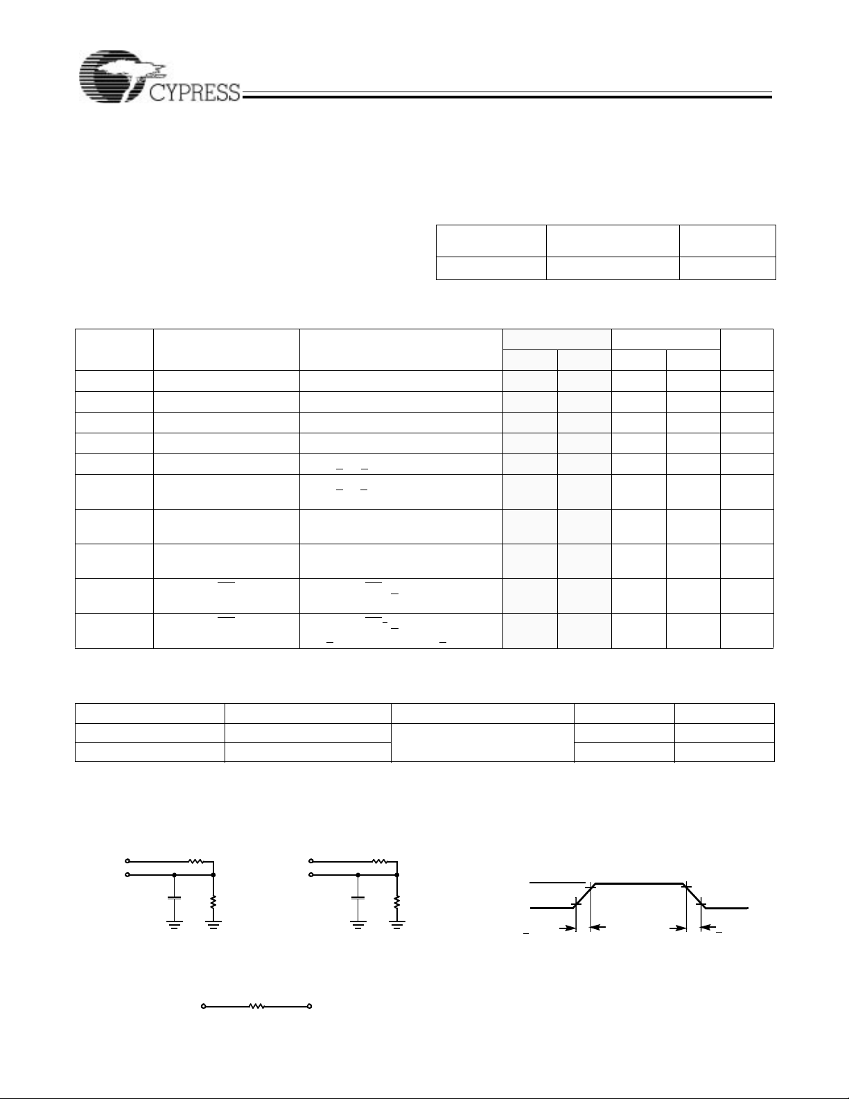
AC Test Loads and Waveforms
R1 481
5V
OUTPUT
30 pF
INCLUDING
JIG AND
SCOPE
Equivalent to: T HÉVENIN EQUIV ALENT
OUTPUT 1.73V
Ω
R2
255Ω
(a) (b)
167Ω
5V
OUTPUT
INCLUDING
JIG AND
SCOPE
5
pF
R1 481Ω
R2
255Ω
CY6264-3
2
3.0V
GND
<
10%
5ns
7 pF
ALL INPUT PULSES
90%
90%
10%
<
CY6264-4
5ns
Page 3
PRELIMINARY
Switching Characteristics Over the Operating Range
[4]
CY6264
6264-55 6264-70
Parameter Descripti on
UnitMin. Max. Min. Max.
READ CYCLE
t
RC
t
AA
t
OHA
t
ACE1
t
ACE2
t
DOE
t
LZOE
t
HZOE
t
LZCE1
t
LZCE2
t
HZCE
t
PU
t
PD
WRITE CYCLE
t
WC
t
SCE1
t
SCE2
t
AW
t
HA
t
SA
t
PWE
t
SD
t
HD
t
HZWE
t
LZWE
Shaded area contains advanced information.
Notes:
4. Test conditions assume signal transition time of 5 ns or less, timing reference levels of 1.5V, input pulse levels of 0 to 3.0V , and output loading of the specified
I
and 30-pF load capacitance.
OL/IOH
5. t
HZOE, tHZCE
6. At any given temperature and voltage condition, t
7. The internal write time of the memory is defined by the overlap of CE
signal can terminate a write by going HIGH. The data input set-up and hold timing should be referenced to the rising edge of the signal that terminates the write.
Read Cycle Time 55 70 ns
Address to Data Valid 55 70 ns
Data Hold from Address Change 5 5 ns
CE1 LOW to Data Valid 55 70 ns
CE2 HIGH to Data Valid 40 70 ns
OE LOW to Data Valid 25 35 ns
OE LOW to Low Z 3 5 ns
OE HIGH to High Z
CE1 LOW to Low Z
[5]
[6]
5 5 ns
20 30 ns
CE2 HIGH to Low Z 3 5 ns
CE1 HIGH to High Z
[5, 6]
20 30 ns
CE2 LOW to High Z
CE1 LOW to Power-Up 0 0 ns
CE1 HIGH to Power-Down 25 30 ns
[7]
Write Cycle Time 50 70 ns
CE1 LOW to Write End 40 60 ns
CE2 HIGH to Write End 30 50 ns
Address Set-Up to Write End 40 55 ns
Address Hold from Write End 0 0 ns
Address Set-Up to Write Start 0 0 ns
WE Pulse Width 25 40 ns
Data Set-Up to Write End 25 35 ns
Data Hold from Write End 0 0 ns
WE LOW to High Z
[5]
20 30 ns
WE HIGH to Low Z 5 5 ns
, and t
are specified with CL = 5 pF as in part (b) of AC Test Loads. Transition is measured ±500 mV from steady-state voltage.
HZWE
is less than t
HZCE
for any given device.
LZCE
LOW , CE2 HIGH, and WE LOW. Both signals must be LOW to initiate a write and either
1
3
Page 4

Switching Waveforms
Read Cycle No.1
ADDRESS
DATA OUT PREVIOUS DATA VALID
Read Cycle No. 2
CE
CE
OE
OE
DATA OUT
V
CC
SUPPLY
CURRENT
[8, 9]
[10, 11]
1
2
t
ACE
t
LZOE
HIGH IMPEDANCE
t
LZCE
t
PU
PRELIMINARY
t
t
OHA
t
50%
DOE
AA
t
RC
CY6264
t
RC
DATA VALID
CY6264-5
t
HZO E
t
DATA VALID
HZCE
t
PD
50%
HIGH
IMPEDANCE
CY6264-6
ICC
ISB
Write Cycle No.1 (WE Controlled)
[9, 11]
ADDRESS
CE
1
CE
2
OE
t
WE
SA
DATA IN
DATA I/O
Notes:
8. Device is continuously selected. OE
9. Address valid prior to or coincident with CE transition LOW.
10. WE is HIGH for read cycle.
11. Data I/O is High Z if OE = VIH, CE1 = VIH, or WE = VIL.
DATA UNDEFINED
, CE = VIL. CE2 = V
IH.
t
t
SCE2
t
SCE1
AW
t
WC
t
HZWE
t
PWE
t
SD
DATAINVALID
t
HA
t
LZWE
HIGH IMPEDANCE
t
HD
CY6264-7
4
Page 5

PRELIMINARY
Switching Waveforms (continued)
Write Cycle No. 2 (CE Cont rolled)
ADDRESS
CE
1
CE
2
WE
DATA IN
DATA I/O
Note:
12. If CE
goes HIGH simultaneously with WE HIGH, the output remains in a high-impedance state.
T y pical DC and AC Characteristics
[9, 11, 12]
t
SA
DATA UNDEFINED
t
AW
CY6264
t
WC
t
SCE1
t
SCE2
t
PWE
DATAINVALID
t
HZWE
t
SD
HIGH IMPEDANCE
t
HA
t
HD
CY6264-8
NORMALIZED SUPPLY CURRENT
vs. SUPP LY VOLTAGE
1.4
1.2
I
1.0
CC
0.8
0.6
0.4
0.2
I
SB
0.0
4.0 4.5 5.0 5.5 6.0
SUPPLY VOLTAGE (V)
NORMALIZED ACCESS TIME
vs. SUP PLY
VOLTAGE
1.4
1.3
1.2
1.1
TA=25°C
1.0
0.9
0.8
4.0 4.5 5.0 5.5 6.0
SUPPLY VOLTAGE (V)
NORMALIZED SUPPLY CURRENT
vs. AMBIENT TEMPERATURE
1.2
1.0
I
CC
0.8
0.6
0.4
0.2
I
SB
0.0
−55 25 125
VCC=5.0V
V
=5.0V
IN
AMBIENT TEMPERATURE (°C)
NORMALIZED ACCESS TIME
vs. AMBIE NT TEMPERATURE
1.6
1.4
1.2
1.0
VCC=5.0V
0.8
0.6
−55 25 125
AMBIENT TEMPERA TURE (°C)
OUTPUT SOURCE CURRENT
vs. OUTPUT
120
VOLTAGE
100
80
=5.0V
V
60
T
CC
=25°C
A
40
20
0
0.0 1.0 2.0 3.0 4.0
OUTPUT VOLTAGE (V)
OUTPUT SINK CURRENT
vs. OUTPUT VOLT AGE
140
120
100
80
V
T
CC
=25°C
A
=5.0V
60
40
20
0
0.0 1.0 2.0 3.0 4.0
OUTPUT VOLTAG E(V)
5
Page 6

PRELIMINARY
T y pical DC and AC Characteristics (continued)
TYPICAL POWER-ON CURRENT
vs. SUPPLY
3.0
2.5
2.0
1.5
1.0
0.5
0.0
0.0 1.0 2.0 3.0 4.0
VOLTAGE
5.0
SUPPLY VOLTAGE(V)
Trut h Table
CE1CE2WE OE Input/Output Mode
H X X X High Z Deselect/Power-Down
X L X X High Z Deselect
L H H L Data Out Read
L H L X Data In Write
L H H H High Z Deselect
TYPICAL ACCESS TIME CHANGE
vs. OUTPUT
30.0
25.0
20.0
15.0
10.0
5.0
0.0
0 200 400 600 800
LOADING
V
T
CAPACITANCE(pF)
CC
=25°C
A
=4.5V
1000
NORMALIZED I
1.25
V
=5.0V
CC
T
=25°C
A
V
=0.5V
CC
1.00
0.75
0.50
10 20 30 40
CYCLE FREQUENCY (MHz)
vs. CYCLE TIME
CC
CY6264
Address Designators
Address
Name
A4 X3 2
A5 X4 3
A6 X5 4
A7 X6 5
A8 X7 6
A9 Y1 7
A10 Y4 8
A11 Y3 9
A12 Y0 10
A0 Y2 21
A1 X0 23
A2 X1 24
A3 X2 25
Address
Function
Pin
Number
6
Page 7

PRELIMINARY
Ordering Info rma tio n
Speed
(ns) Ordering Code
55 CY6264-55SC S23 28-Lead 330-Mil SOIC
70 CY6264-70SC S23 28-Lead 330-Mil SOIC
55 CY6264-55SNC S22 28-Lead 300-Mil SOIC Commercial
70 CY6264-70SNC S22 28-Lead 300-Mil SOIC Commercial
Shaded area contains advanced information.
Note:
13. Not recommended for new designs.
Document #: 38-00425-A
Package Diagrams
Package
Name Package Type
[13]
[13]
28-Lead 450-Mil (300-Mil Body Width) SOIC S22
Commercial
Commercial
CY6264
Operating
Range
7
Page 8

Package Diagrams (continued)
PRELIMINARY
28-Lead (330-Mil) SOIC
CY6264
S23
© Cypress Semiconductor Corporation, 1996. The information contained herein is subject to change without notice. Cypress Semiconductor Corporation assumes no responsibility for the use
of any circ uitry other than circui try embodi ed in a Cypress Semi conductor p roduct. Nor does it convey or imply any li cense under patent or other rights . Cypress Semi conductor does not authori ze
its products for use as critical components in life-support systems where a malfunction or failure may reasonably be expected to result in significant injury to the user. The inclusion of Cypress
Semiconductor products in life-support systems application implies that the manufacturer assumes all risk of such use and in doing so indemnifies Cypress Semiconductor against all charges.
 Loading...