

Datasheet CY62148V-70SCT, CY62148V-70SC, CY62148LL-70SCT, CY62148LL-70SC, CY62148L-70SCT Datasheet (Cypress Semiconductor)
...Page 1
512K x 8 MoBL Static RAM
CY62148V MoBL™
Cypress Semiconductor Corporation
• 3901 North First Street • San Jose • CA 95134 • 408-943-2600
March 23, 2000
MoBL
Features
• Low volt age rang e :
—2.7V–3.6V
• Ultra lo w acti ve pow er
• Low st a ndby powe r
• TTL-compatible inputs and outputs
• Autom atic power-d ow n w hen deselected
• CMOS for optimum spee d/power
Functional Description
The CY62148V is a high-performance CMOS static RAM organized as 524,288 words by 8 bits. This device features advanced circuit design to provide ultra-low active current. This
is ideal for providing More Battery Lif e™ (MoBL™) in portable
applications such as cellular telephones. The device also has
an automatic power-down feature that significantly reduces
power consum ption b y 99% when addresses are not toggl ing.
The device can be put into standby mode when deselected
(CE
HIGH).
Writing to the device is accomplished by taking Chip Enable
(CE
) and Write Enable ( WE) inputs LO W . Dat a on the eigh t I/O
pins (I/O
0
through I/O7) is then written into the location speci-
fied on the address pins (A
0
through A18).
Reading from the device is accomplished by taking Chip Enable (CE
) and Output Enable (OE) LOW while forcing Write
Enable (WE
) HIGH. Under these conditions, the contents of
the memory locati on specified by the ad dress pins will appear
on the I/O pins.
The eight input/output pins (I/O
0
through I/O7) are placed in a
high-impedance state when the device is deselected (CE
HIGH), the outputs are disabled (OE HIGH), or during a write
operation (CE
LOW and WE LOW).
The CY62148V is avai labl e in a 36-ball FBGA, 32 pi n TSOPII,
and a 32-pin SOIC package.
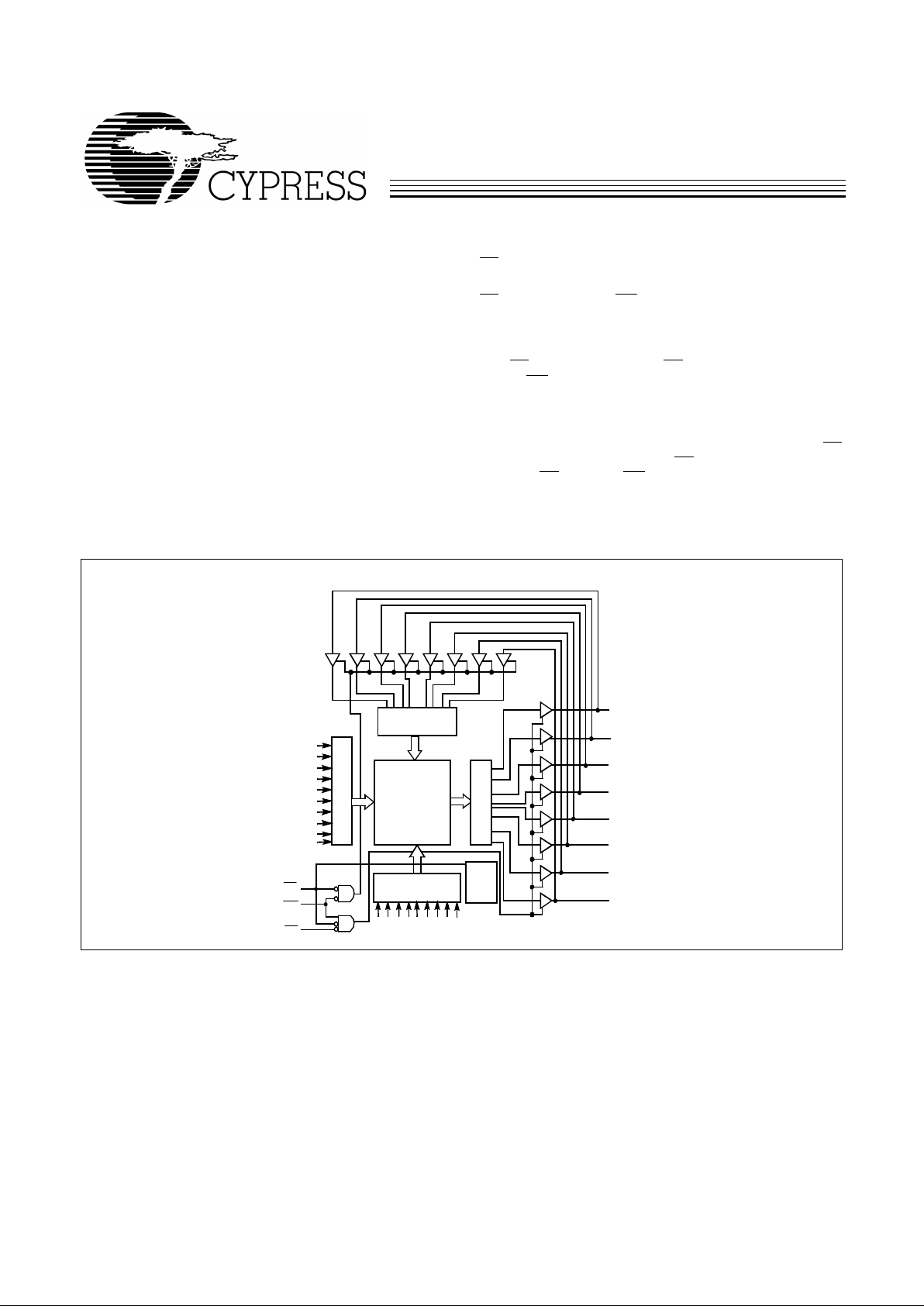
Logic Block Diagram
17
15
A
1
A
2
A
3
A
4
A
5
A
6
A
7
A
8
COLUMN
DECODER
ROW DECODER
SENSE AMPS
Data in Drivers
POWER
DOWN
WE
OE
I/O
0
I/O
1
I/O
2
I/O
3
512K x 8
ARRAY
I/O
7
I/O
6
I/O
5
I/O
4
A
0
A
12
A14A
13
A
A
11
CE
A
A
16
A
10
62148V-1
18
A
A
9
Page 2
CY62148V MoBL™
2
Maximum Ratings
(Above which the useful life may be impaired. For user guidelines, not tested.)
Storage Temperature ......................... .. .. ....–65°C to +150 °C
Ambient Temperature with
Power Applied............................................... 55°C to +125°C
Supply Voltage to Ground Potential...............–0.5V to +4.6V
DC V oltage Applied to Outputs
in High Z State
[1]
....................................–0.5V to VCC + 0.5V
DC Input Voltage
[1]
................................–0.5V to VCC + 0.5V
Output Current into Outputs (LOW)............................. 20 mA
Static Discharge Voltage ................. ...................... ... >2001V
(per MIL-STD-883, Method 3015)
Latch-Up Current............. .. .......... .. .......... .. .......... .. . >200 mA
Notes:
1. V
IL(min.)
= –2.0V for pulse durations less than 20 ns.
2. Typical values are included for reference only and are not guaranteed or tested. Typical values are measured at V
CC
= V
CC(typ.)
, TA = 25°C.
Pin
Configurations
WE
1
2
3
4
5
6
7
8
9
10
11
14
31
32
Top View
12
13
16
15
29
30
V
CC
A
3
A
2
A
1
A
17
A
16
OE
A
6
A
14
CE
I/O
2
I/O
0
I/O
1
A
12
A
7
21
22
19
20
I/O
7
27
28
25
26
17
18
23
24
V
SS
A
5
A
4
I/O
6
I/O
5
I/O
4
I/O
3
A
10
A
18
A
11
TSOPII/SOIC
A
0
A
15
V
CC
A
13
A
12
A
5
NC
WE
A
7
I/O
4
I/O
5
A
4
NC
I/O
6
I/O
7
V
SS
A
11
A
10
A
1
V
SS
I/O
0
A
2
A
8
A
6
A
3
A
0
V
CC
I/O
1
I/O
2
I/O
3
A
17
A
18
A
16
CE
OE
A
9
A
14
62148V–2
3265
4
1
D
E
B
A
C
F
G
H
T op View
FBGA
A
9
A
8
A
13
A
15
Operating Range
Range Ambient Tem perature V
CC
Industrial –40°C to +85°C 2.7V to 3.6V
Product Portfolio
Product VCC Range
Speed
Power Dissipation (Industrial)
Operating (ICC) Standby (I
SB2
)
Min. Typ.
[2]
Max. Typ.
[2]
Maximum Ty.p
[2]
Maximum
CY62148V 2.7V 3.0V 3.6V 70 ns 7 15 mA 2 µA 20 µA
Page 3
CY62148V MoBL™
3
Electrical Characteristics
Over the Operating Range
CY62148V
Parameter Description Test Conditions Min. Typ.
[2]
Max. Unit
V
OH
Outp ut HIGH Voltage IOH = –1.0 mA VCC = 2.7V 2.4 V
V
OL
Output LOW Voltage IOL = 2.1 mA VCC = 2.7V 0.4 V
V
IH
Input HIGH Voltage VCC = 3.6V 2.2 V
CC
+ 0.5V V
V
IL
Input LOW Voltage VCC = 2.7V –0.5 0.8 V
I
IX
Input Load Current GND < VI < V
CC
–1 +1 +1
µA
I
OZ
Output Leakage Current GND < VO < VCC, Output
Disabled
–1 +1 +1
µA
I
CC
VCC Operating Supply
Curr ent
I
OUT
= 0 mA, (f =
f
MAX
= 1/tRC) CMOS
Levels
VCC = 3.6V 7 15 mA
I
OUT
= 0 mA, f = 1 MHz CMOS Le v el s 1 2 mA
I
SB1
Auto matic CE
Power-Down Current—
CMOS Inputs
CE > VCC − 0.3V,
V
IN
> VCC − 0.3V or
V
IN
< 0.3V, f = f
MAX
100
µA
I
SB2
Auto matic CE
Power-Down Current—
CMOS Inputs
CE > V
CC
− 0.3V
V
IN
> V
CC
− 0.3V
or V
IN
< 0.3V, f = 0
L 1 50
µA
VCC =
3.6V
LL 2 20
µA
Capacitance
[3]
Parameter Description Test Conditions Max. Unit
C
IN
Input Capacitance TA = 25°C, f = 1 MHz,
V
CC
= 3.0V
6 pF
C
OUT
Output Capacitance 8 pF
Thermal Resistance
Description T est Condi tions Symbol Others BGA Units
Thermal Resistance
[3]
(Junction to Ambient)
Still Air , soldered on a 4.25 x 1 .125 inch, 4-lay er
printed circuit board
Θ
JA
TBD TBD °C/W
Thermal Resistance
[3]
(Junction to Case)
Θ
JC
TBD TBD °C/W
Note:
3. Tested initially and after any design or process changes that may affect these parameters.
Page 4
CY62148V MoBL™
4
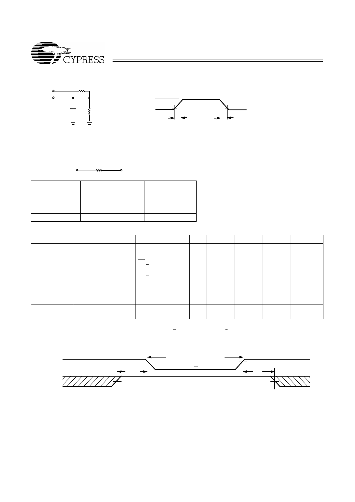
AC Test Loads and Waveforms
Parameters 3.0V Unit
R1 1105 Ohms
R2 1550 Ohms
R
TH
645 Ohms
V
TH
1.75V Volts
Data Rete n ti o n C h ar acteristics
(Over the Operating Range)
Parameter Description Conditions Min. Typ.
[2]
Max. Unit
V
DR
VCC for Da ta Rete ntion 1.0 3.6 V
I
CCDR
Data Retention Current VCC = 1.0V
CE
> V
CC
− 0.3V ,
V
IN
> VCC − 0.3V or
V
IN
< 0.3V
No input may exceed
V
CC
+0.3V
L/ LL 0.2 5.5
µA
µA
t
CDR
[3]
Chip Deselect to Data
Retention Time
0 ns
t
R
[4]
Operation Recov ery
Time
t
RC
ns
Note:
4. Full Device AC operation requires linear V
CC
ramp from V
DR
to V
CC(min.)
> 10 µs or stable at V
CC(min.)
> 10 µs.
Data Retention Waveform
VCC Typ
V
CC
OUTPUT
R2
30 pF
INCLUDING
JIG AND
SCOPE
GND
90%
10%
90%
10%
OUTPUT V
TH
Equivalent to: THÉ VENIN EQUIVALENT
ALL INPUT PULSES
62148V–3
62148V–4
R
TH
R1
Fall time: 1 V/ns
Rise Time: 1 V/ns
62148V–5
1.0V1.0V
t
CDR
VDR> 1.0 V
DATA RETENTION MODE
t
R
CE
V
CC
Page 5

CY62148V MoBL™
5
Switching Characteristics
Over the Operating Range
[5]
(2.7V–3.6V
Operation)
Parameter Description Min. Max. Unit
READ CYCLE
t
RC
Read Cycle Time 70 ns
t
AA
Address to Data Valid 70 ns
t
OHA
Data Hold from Address Change 10 ns
t
ACE
CE LOW to Data Valid 70 ns
t
DOE
OE LOW to Data Valid 35 ns
t
LZOE
OE LOW to Low Z
[6]
5 ns
t
HZOE
OE HIGH to High Z
[7 ]
25 ns
t
LZCE
CE LOW to Low Z
[6]
10 ns
t
HZCE
CE HIGH to High Z
[6, 7]
25 ns
t
PU
CE LOW to Power-Up 0 ns
t
PD
CE HIGH to Power-Do wn 70 ns
WRITE CYCLE
[8, 9]
t
WC
Write Cycle Time 70 ns
t
SCE
CE LOW to Write End 60 ns
t
AW
Address Set-Up to Write End 60 ns
t
HA
Address Hold from Write End 0 ns
t
SA
Address Set-Up to Write Start 0 ns
t
PWE
WE Pulse Width 50 ns
t
SD
Data Set-Up to Write End 30 ns
t
HD
Data Hold from Write End 0 ns
t
HZWE
WE LOW to High Z
[6, 7]
25 ns
t
LZWE
WE HIGH to Low Z
[6]
10 ns
Notes:
5. Test conditions assume signal transition time of 5 ns or less, timing reference levels of 1.5V, input pulse levels of 0 to V
CC(typ.)
, and output loading of the
specified I
OL/IOH
and 30 pF load capacitance.
6. At any given temperature and voltage condition, t
HZCE
is less than t
LZCE
, t
HZOE
is less than t
LZOE
, and t
HZWE
is less than t
LZWE
for any given device.
7. t
HZOE
, t
HZCE
, and t
HZWE
are specified with CL = 5 pF as in part (b) of AC Test Loads. Transition is measured ±200 mV from steady-state voltage.
8. The internal write time of the memory is defined by the overlap of CE
LOW and WE LOW. Both signals must be LOW to initiate a write and either signal can
terminate a write by going HIGH. The data input set-up and hold timing should be referenced to the rising edge of the signal that terminates the write.
9. The minimum write cycle time for Write Cycle #3 (WE
controlled, OE LOW) is the sum of t
HZWE
and tSD.
Page 6

CY62148V MoBL™
6
Switching Wavefor ms
Notes:
10. Device is continuously selected. OE
, CE = VIL.
11. WE
is HIGH for read cycle.
12. Address valid prior to or coincident with CE transition LOW.
13. Data I/O is high impedance if OE
= VIH.
14. If CE
goes HIGH simultaneously with WE HIGH, the output remains in a high-impedance state.
15. During this period, the I/Os are in output state and input signals should not be applied.
ADDRESS
DATA OUT PREVIOUS DATA VALID
DATA VALID
t
RC
t
AA
t
OHA
62148V–6
Read Cycle No. 1
[10, 1 1]
50%
50%
DATA VALID
t
RC
t
ACE
t
DOE
t
LZOE
t
LZCE
t
PU
DATA OUT
HIGH IMPEDANCE
IMPEDANCE
I
CC
I
SB
t
HZOE
t
HZCE
t
PD
OE
CE
HIGH
V
CC
SUPPLY
CURRENT
62148V–7
Read Cycle No. 2
[11, 12]
t
HD
t
SD
t
PWE
t
SA
t
HA
t
AW
t
WC
DATA I/O
ADDRESS
CE
WE
OE
t
HZOE
62148V–8
DATAINVALID
NOTE
Write Cycle No. 1 (WE Controlled)
[8, 13, 14]
15
Page 7

CY62148V MoBL™
7
Switching Wavefor ms
(continued)
t
WC
t
AW
t
SA
t
HA
t
HD
t
SD
t
SCE
WE
DATA I/O
ADDRESS
CE
62148V–9
DATAINVALID
Write Cycle No. 2 (CE Controlled)
[8, 13 , 14]
DATA I/O
ADDRESS
t
HD
t
SD
t
LZWE
t
SA
t
HA
t
AW
t
WC
CE
WE
t
HZWE
62148–10
DATAINVALID
Write Cycle No. 3 (WE Controlled, OE LOW)
[9, 14]
NOTE 15
Page 8

CY62148V MoBL™
8
Typical DC and AC Characteristics
Truth Table
CE WE OE Inputs/Outputs Mode Power
H X X High Z Deselect/Power-Down Standby (ISB)
L H L Data Out Read Active (ICC)
L L X Data In Write Active (ICC)
L H H High Z Output Disabled Active (ICC)
70
80
60
40
30
20
1.0
1.9
2.8
3.7
SUPPLY VOLTAGE (V)
Access Time vs. Supp ly Volt age
10
50
T
AA
(ns)
40
45
35
25
20
15
1.0
1.9
2.8
3.7
10
30
I
SB (
µ
A)
Standby Curren t vs. Supply Voltage
SUPPLY VOLTAGE (V)
1.2
1.4
1.0
0.6
0.4
0.2
1.7 2.2 2.7 3.2 3.7
0.0
0.8
I
CC
Normalized Operating Current
SUPPLY VOLTAGE (V)
vs. Supply Voltage
Page 9

CY62148V MoBL™
9
Document #: 38-00646-C
Ordering Information
Speed
(ns) Ordering Code
Package
Name Package Type
Operating
Range
70 CY62148VLL-70BAI BA37 36-Ball Fine Pitch BGA Industrial
CY62148VLL-70ZI ZS32 32-Lead TSOPII
CY62148VLL-70SI S34 32-Lead 450 mil. molded SOIC
Package Diagrams
36-Ball (7.00 mm x 8.5 mm x 1.5 mm) Thin BGA BA37
51-85105-A
Page 10

CY62148V MoBL™
10
Package Diagrams
(continued)
32-Lead (450 MIL) Molded SOIC S34
Page 11

CY62148V MoBL™
© Cypress Semiconductor Corporation, 1999. The information contained herein is subject to change without notice. Cypress Semiconductor Corporation assumes no responsibility for the use
of any circuitry other than circuitry embodied in a Cypress Semiconduc tor product. Nor does it convey or imply any license under patent or other rights. Cypress Semiconductor does not authori ze
its products for use as critical components in life-support systems where a malfunction or failure may reasonably be expected to result in significant injury to the user. The inclusion of Cypress
Semiconductor products in life-support systems application implies that the manufacturer assumes all risk of such use and in doing so indemnifies Cypress Semiconductor against all charges.
Package Diagrams
(continued)
32-Lead
TSOP II ZS32
51-85095
 Loading...