

Page 1
CY62147V MoBL
®
4M (256K x 16) Static RAM
Features
• Wide voltage range: 2.7V–3.6V
• Ultra-lo w active, standby power
• Easy memory expansion with C E
and OE features
• TTL-compatible inputs and outputs
• Automatic power-down when deselec ted
• CMOS for optimum speed/power
• Package available in a standard 44-pin TSOP Type II
(forward pinout) package
Functional Description
[1]
The CY62147V is a high-performance CMOS static RAM
organized as 256K words by 16 bits. These devices feature
advanced circuit design to provide ultra-low active current.
This is ideal for providing More Battery Life (MoBL
®
) in
portable applicati ons such as cellular tel ephones. The devices
also have an automatic power-down feature that significantly
reduces power consumption by 99% when addresses are not
toggling. The device c an a lso be pu t into standby mode when
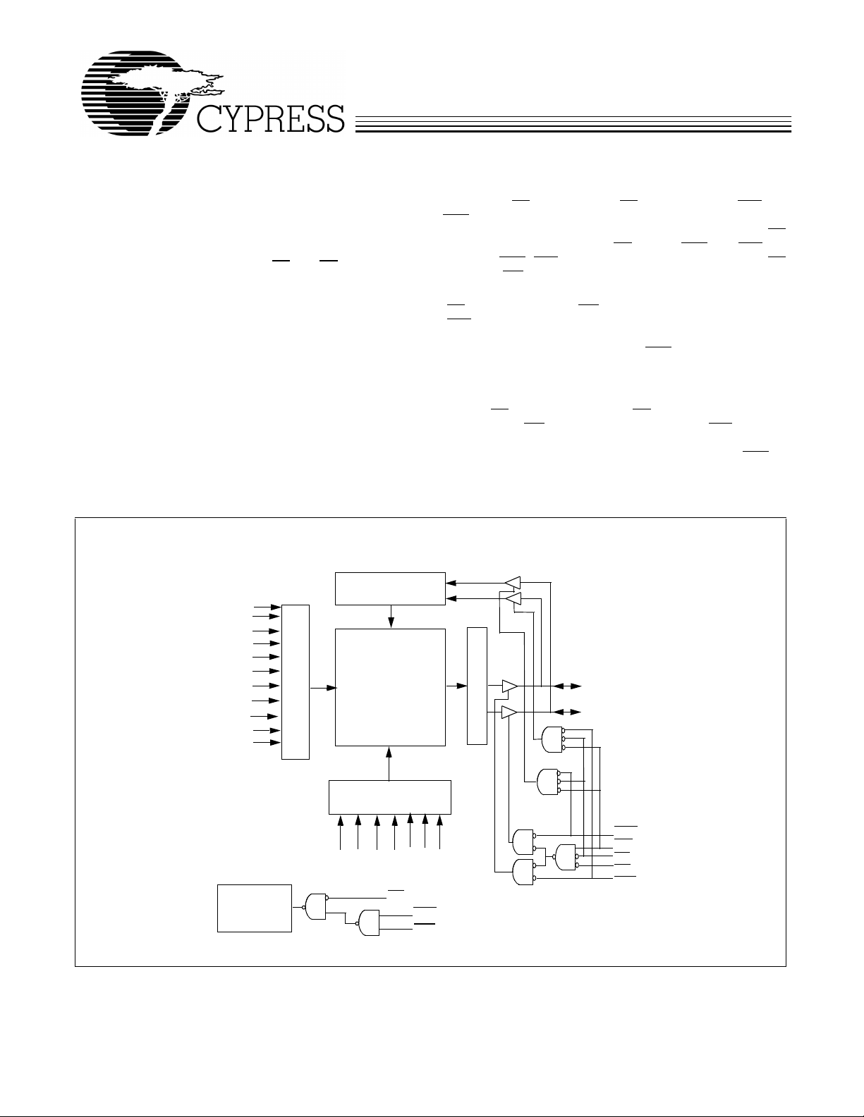
Logic Block Diagram
DATA IN DRIVERS
A
10
A
9
A
8
A
7
A
6
A
5
A
4
A
3
A
2
A
1
A
0
ROW DECODER
256K x 16
RAM Array
2048 x 2048
deselected (CE
are HIGH. The input/output pins (I/O0 through I/O15) are
BHE
HIGH) or when CE is LOW and both BLE and
placed in a high-impedance state when: deselected (CE
HIGH), outputs are disabled (OE HIGH), BHE and BLE are
disabled (BHE
, BLE HIGH), or during a write operation ( CE
LOW, and WE LOW).
Writing to the device is accomplished by taking Chip Enable
) and Write Enabl e (WE) inputs LOW. If Byte Low Enable
(CE
) is LOW, then data from I/O pins (I/O0 through I/O7), is
(BLE
written into the location specified on the address pins (A
through A17). If Byte High Enable (BHE) is LOW, then data
from I/O pins (I/O
specified on the address pins (A
through I/O15) is written into the location
8
through A17).
0
Reading from the device is accomplished by taking Chip
Enable (CE
) and Output Enable (OE) LOW while forcing the
Write Enable (WE) HIGH. If Byte Low Enable (BLE) is LOW,
then data from the memory location specified by the address
pins will appear on I/O
LOW , then data from memory will app ear on I/O8 to I/O15. See
to I/O7. If Byte High Enable (BHE) is
0
the truth table at the back of this data sheet for a complete
description of read and write modes.
I/O
– I/O
0
7
SENSE AMPS
I/O8 – I/O
15
0
COLUMN DECODER
BHE
11
13
A
A12A
Power-down
Circuit
Note:
1. For best practice recommendations, please refer to the Cypress application note “System Design Guidelines” on http ://www.cypress.com.
CE
16
15
A
BHE
BLE
17
A
A
14
A
WE
CE
OE
BLE
Cypress Semiconductor Corporation • 3901 North First Street • San Jose • CA 95134 • 408-943-2600
Document #: 38-05050 Rev. *A Revised August 28, 2002
Page 2

Pin Configurations
TSOP II (Forward)
Top View
Maximum Ratings
(Above which the us efu l l ife may be impaired. For user gui delines, not tested.)
Storage Temperature .................................–65°C to +150°C
Ambient Temperature with
Power Applied.............................................–55°C to +125°C
Supply Voltage to Ground Potential...............–0.5V to +4.6V
DC Voltage Applied to Outputs
in High-Z State
[2]
....................................–0.5V to VCC + 0.5V
CE
I/O
I/O
I/O
I/O
V
V
I/O
I/O
I/O
I/O
WE
A
A
A
A
A
A
A
A
A
A
CC
SS
4
3
2
1
0
0
1
2
3
4
5
6
7
16
15
14
13
12
CY62147V MoBL
44
1
2
3
4
5
6
7
8
9
10
11
12
13
14
15
16
17
18
19
20
21
22
A
5
43
A
6
42
A
7
41
OE
40
BHE
39
BLE
38
I/O
15
37
I/O
14
36
I/O
13
35
I/O
12
34
V
SS
33
V
CC
32
I/O
11
I/O
31
10
30
I/O
9
29
I/O
8
28
NC
27
A
8
26
A
9
A
25
10
A
24
11
23
A
17
[2]
DC Input Voltage
................................–0.5V to VCC + 0.5V
Output Current into Outputs (LOW).............................20 mA
Static Discharge Voltage.......................................... > 2001V
(per MIL-STD-883, Method 3015)
Latch-up Current.................................................... > 200 mA
Operating Range
Range
Industrial –40°C to +85°C 2.7V to 3.6V
Ambient
Temperature V
®
CC
Product Portfolio
Power Dissipation
Product
VCC Range (V)
V
CC(min.)VCC(typ.)
[3]
V
CC(max.)
Speed
(ns)
Operating ICC, (mA) Standby I
Typ.
[3]
Maximum Typ.
[3]
, (µA)
SB2
Maximum
CY62147VLL 2.7 3.0 3.6 70 7 15 2 20
Electrical Characteristics Over the Operating Range
CY62147V-70
Parameter Description Test Conditions
V
OH
V
OL
V
IH
V
IL
I
IX
I
OZ
I
CC
Notes:
2. V
3. Typical values are included for reference only and are not guaranteed or tested. Typical values are measured at V
Output HIGH Voltage IOH = –1.0 mA VCC = 2.7V 2.4 V
Output LOW Voltage IOL = 2.1 mA VCC = 2.7V 0.4 V
Input HIGH V oltage VCC = 3.6V 2.2 VCC +
Input LOW Vo lt a ge V
Input Load Current GND < VI < V
Output Leakage
GND < VO < VCC, Output Disabled –1 +1 +1 µA
CC
= 2.7V –0.5 0.8 V
CC
Current
VCC Operating Supply
Current
= –2.0V for pulse durations less than 20 ns.
IL(min.)
I
= 0 mA, f = f
OUT
Levels
I
= 0 mA, f = 1 MHz, CMOS Levels 1 2 mA
OUT
= 1/tRC, CMOS
MAX
VCC = 3.6V 7 15 mA
–1 ±1 +1 µA
= V
CC
CC(typ.)
[3]
, TA = 25°C.
Max.
UnitMin. Typ.
V
0.5V
Document #: 38-05050 Rev. *A Page 2 of 9
Page 3
CY62147V MoBL
Electrical Characteristics Over the Operating Range (continued)
CY62147V-70
Parameter Description Test Conditions
I
SB1
I
SB2
Automatic CE
Power-down Current—
CMOS Inputs
Automatic CE
Power-down Current—
CE > VCC – 0.3V, VIN > VCC – 0.3V or VIN
0.3V, f = f
<
MAX
CE > VCC – 0.3V, VIN > VCC – 0.3V , or VIN
0.3V, f = 0
<
VCC = 3.6V
[3]
Max.
2 20 µA
CMOS Inputs
Capacitance
[4]
Parameter Description Test Conditions Max. Unit
C
C
IN
OUT
Input Capacitance TA = 25°C, f = 1 MHz,
= V
V
CC
Output Capacitance 8 pF
CC(typ.)
6 pF
Thermal Resistance
Parameter Description Test Conditions BGA TSOPII Units
Θ
Θ
Thermal Resistance
JA
(Junction to Ambient)
Thermal Resistance
JC
(Junction to Case)
[4]
[4]
Still Air , soldered on a 4.25 x 1.12 5 inch, 4-layer
printed circuit board
55 60 °C/W
16 22 °C/W
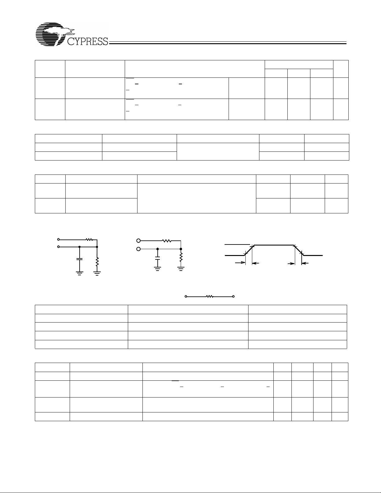
AC Test Loads and Waveforms
®
UnitMin. Typ.
V
CC
OUTPUT
INCLUDING
30 pF
JIG AND
SCOPE
R1
(a)
R2
V
CC
OUTPUT
INCLUDING
JIG AND
SCOPE
Equivalent to: THÉ VENIN EQUIVALENT
5 pF
R1
VCC Typ
R2
GND
Rise TIme: 1 V/ns Fall Time: 1 V/ns
(b)
R
OUTPUT V
TH
10%
ALL INPUT PULSES
90%
(c)
TH
Parameter 3.0V Unit
R1 110 5 Ω
R2 1550 Ω
R
TH
V
TH
645 Ω
1.75 V
Data Retention Characteristics (Over the Operating Range)
Parameter Description Conditions Min. Typ.
V
DR
I
CCDR
[4]
t
CDR
[5]
t
R
Note:
4. Tested initially and after any design or process changes that may affect these parameters.
VCC for Data Retention 1.0 3.6 V
Data Retention Current V
Chip Deselect to Data
= 1.0V , CE > VCC – 0.3V, VIN > VCC – 0.3V or VIN <
CC
0.3V; No input may exceed V
CC
+ 0.3V
0 ns
Retention Time
Operation Recovery Time 70 ns
90%
10%
[3]
Max. Unit
1 10 µA
Document #: 38-05050 Rev. *A Page 3 of 9
Page 4

Data Retention Waveform
CY62147V MoBL
®
V
V
CC
CC(min.)
t
CDR
VDR> 1.0 V
V
CC(min.)
t
R
CE
DATA RETENTION MODE
Switching Characteristics Over the Operating Range[
6]
70 ns
Parameter Description
Read Cycle
t
RC
t
AA
t
OHA
t
ACE
t
DOE
t
LZOE
t
HZOE
t
LZCE
t
HZCE
t
PU
t
PD
t
DBE
[8]
t
LZBE
t
HZBE
Write Cycle
t
WC
t
SCE
t
AW
t
HA
t
SA
t
PWE
t
BW
t
SD
t
HD
t
HZWE
t
LZWE
Notes:
5. Full Device AC operation requires linear V
6. Test conditions assume signal transition time of 5 ns or less, timing reference levels of 1.5V, input pulse levels of 0 to V
specified I
7. At any given temperature and voltage condition, t
8. If both byte enables are toggled together this value is 10ns
9. t
10. The internal write time of the memory is defined by the overlap of CE
terminate a write by going HIGH. The data input set-up and hold timing should be referenced to the rising edge of the signal that terminates the write.
11. The minimum write cycle time for Write Cycle #3 (WE
HZOE
, t
[10, 11]
and 30 pF load capacitance.
OL/IOH
HZCE
, and t
are specified with CL = 5 pF as in part (b) of AC Test Loads. Transition is measured ±500 mV from steady-state voltage.
HZWE
Read Cycle Time 70 ns
Address to Data Valid 70 ns
Data Hold from Address Change 10 ns
CE LOW to Data Valid 70 ns
OE LOW to Data Valid 25 ns
OE LOW to Low-Z
OE HIGH to High-Z
CE LOW to Low-Z
CE HIGH to High-Z
[7, 9]
[9]
[7]
[7, 9]
5 ns
20 ns
10 ns
20 ns
CE LOW to Power-up 0 ns
CE HIGH to Power-down 70 ns
BHE / BLE LOW to Data Valid 70 ns
BHE / BLE LOW to Low-Z 5 ns
BHE / BLE HIGH to High-Z 20 ns
Write Cycle Time 70 ns
CE LOW to Write End 60 ns
Address Set-up to Write End 60 ns
Address Hold from Write End 0 ns
Address Set-up to Write Start 0 ns
WE Pulse Width 40 ns
BHE / BLE Pulse Width 60 ns
Data Set-up to Write End 30 ns
Data Hold from Write End 0 ns
WE LOW to High-Z
WE HIGH to Low-Z
ramp from V
CC
HZCE
[7, 9]
[7]
to V
DR
is less than t
controlled, OE LOW) is the sum of t
> 10 µs or stable at V
CC(min.)
, t
LZCE
LOW and WE LOW. Both signals must be LOW to initiate a write and either signal can
is less than t
HZOE
LZOE
HZWE
CC(min.)
, and t
and tSD.
25 ns
10 ns
>10 µs.
HZWE
is less than t
, and output loading of the
CC(typ.)
for any given device.
LZWE
UnitMin. Max.
Document #: 38-05050 Rev. *A Page 4 of 9
Page 5
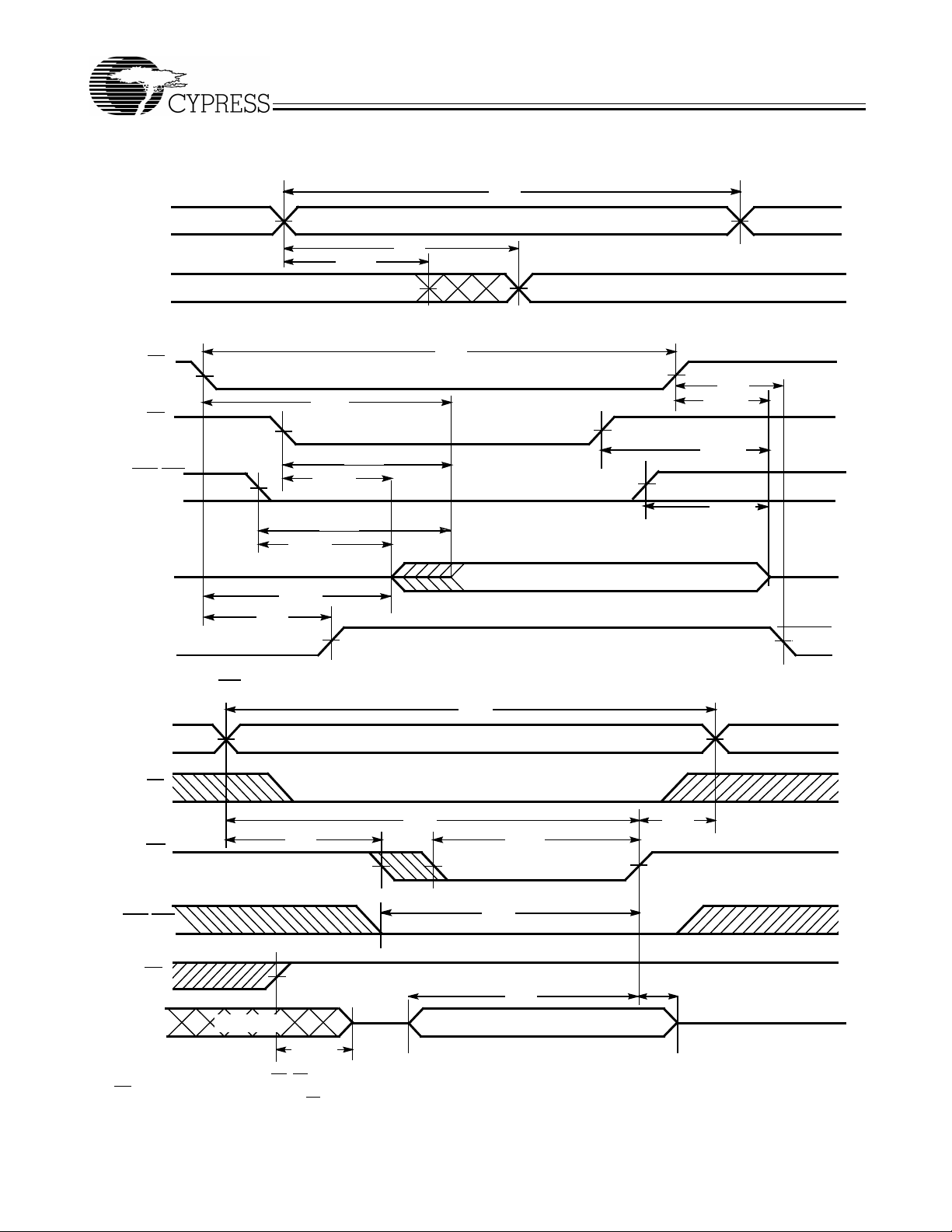
Switching Waveforms
Read Cycle No. 1
ADDRESS
DATA OUT PREVIOUS DATA VALID
[12, 13]
t
OHA
t
RC
t
AA
CY62147V MoBL
®
DATA VALID
Read Cycle No. 2
[13, 14]
CE
OE
BHE/BLE
t
LZBE
DATA OUT
V
CC
SUPPLY
HIGH IMPEDANCE
t
LZCE
t
PU
CURRENT
Write Cycle No. 1 (WE Controlled)
ADDRESS
t
ACE
t
DOE
t
LZOE
t
DBE
50%
[10, 15, 16]
t
RC
t
PD
t
HZCE
t
HZOE
t
HZBE
HIGH
50%
IMPEDANCE
I
CC
I
SB
t
DATA VALID
WC
CE
t
HA
WE
BHE/BLE
t
AW
t
SA
t
PWE
t
BW
OE
DATA I/O
Notes:
12. Device is continuously selected. OE
is HIGH for read cycle.
13. WE
14. Address valid prior to or coincident with CE transition LOW .
NOTE
17
t
HZOE
, CE = VIL.
t
SD
DATAINVALID
t
HD
Document #: 38-05050 Rev. *A Page 5 of 9
Page 6
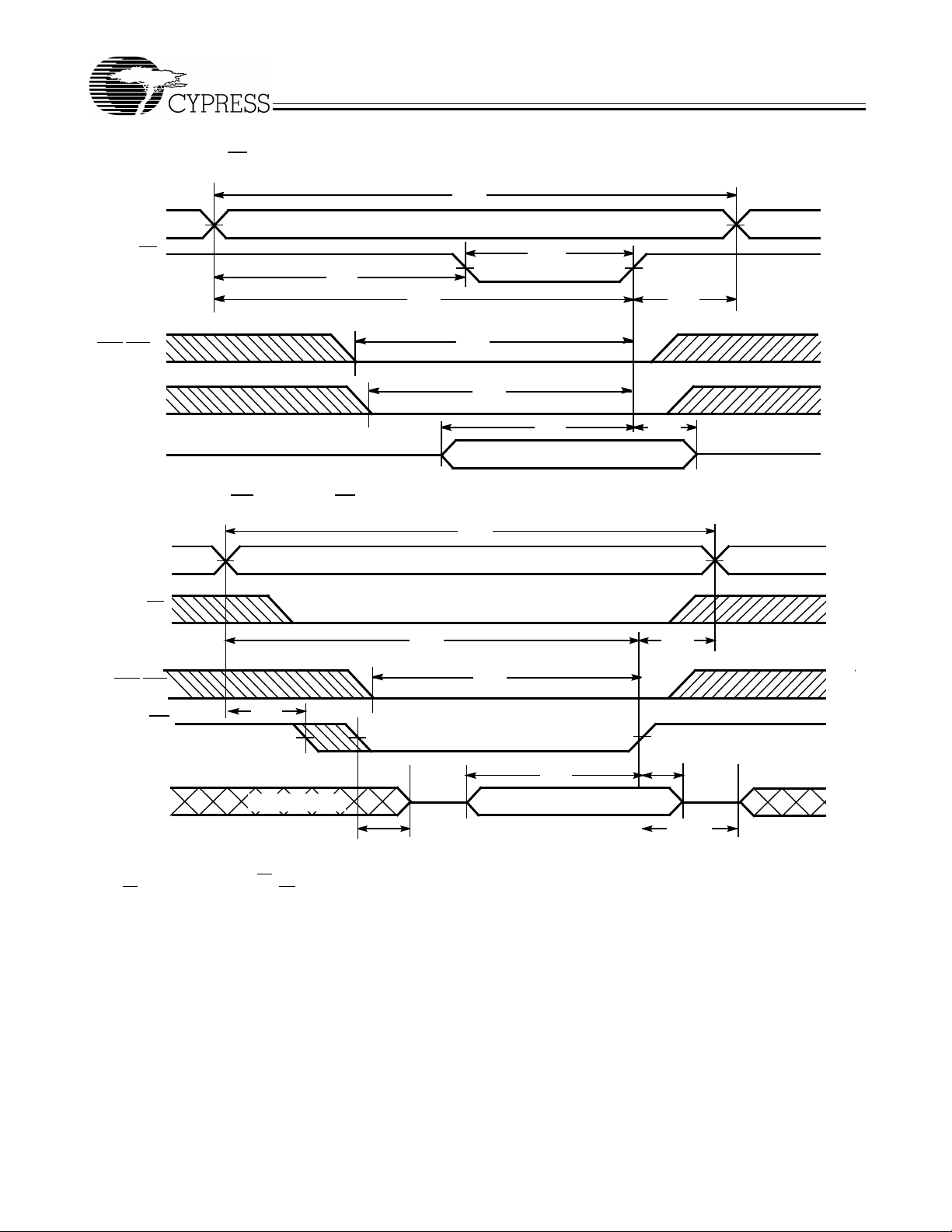
Switching Waveforms (continued)
Write Cycle No. 2 (CE Controlled)
ADDRESS
[8, 15, 16]
t
WC
CY62147V MoBL
®
CE
t
SA
BHE/BLE
WE
DATA I/O
Write Cycle No. 3 (WE Controlled, OE LOW)
ADDRESS
CE
BHE/BLE
t
WE
SA
t
AW
[11, 16 ]
t
AW
t
BW
t
WC
t
PWE
t
BW
t
SCE
t
SD
DATAINVALID
t
HA
t
HD
t
HA
DATA I/O
Notes:
15. Data I/O is high-impedance if OE
16. If CE
17. During this period, the I/Os are in output state and input signals should not be applied.
goes HIGH simultaneously wit h WE HIGH, the ou tput remains in a h igh-impeda nce s tat e.
NOTE 17
= VIH.
t
HZWE
t
SD
DATAINVALID
t
LZWE
t
HD
Document #: 38-05050 Rev. *A Page 6 of 9
Page 7
Switching Waveforms (continued)
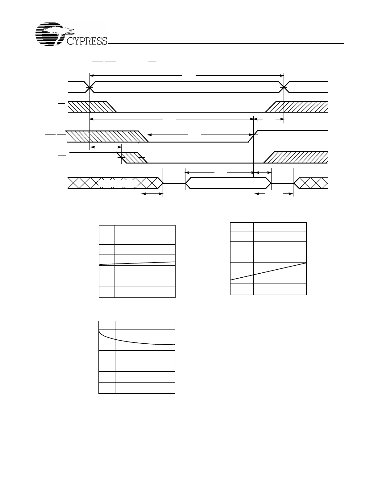
Write Cycle No. 4 (BHE/BLE Controlled, OE LOW)
ADDRESS
CE
[17]
t
WC
CY62147V MoBL
®
BHE/BLE
t
SA
WE
DATA I/O
NOTE 17
t
HZWE
Typical DC and AC Characteristics
Normalized Operating Current
1.4
1.2
1.0
0.8
CC
I
0.6
0.4
0.2
0.0
80
70
2.7 2.8
vs. Supply Voltage
SUPPLY VOLTAGE (V)
Access Time vs. Supply Voltage
MoBL
MoBL
t
AW
3.7
t
BW
t
HA
t
SD
DATAINVALID
Standby Current vs. Supply Voltage
45
40
35
30
SB (µA)
20
I
15
10
5
2.7 2.8
SUPPLY VOLTAGE (V)
t
LZWE
t
HD
MoBL
3.7
60
50
40
AA (ns)
30
T
20
10
2.8 3.7
2.7
SUPPLYVOLTAGE (V)
Document #: 38-05050 Rev. *A Page 7 of 9
Page 8
CY62147V MoBL
Truth Table
CE WE OE BHE BLE Inputs/Outputs Mode Power
H X X X X High-Z Deselect/Power-down Standby (ISB)
L X X H H High-Z Deselect/Power-down Standby (ISB)
L H L L L Data Out (I/OO–I/O15) Read Active (ICC)
L H L H L Data Out (I/OO–I/O7);
I/O8–I/O
in High-Z
15
L H L L H Data Out (I/O8–I/O15);
–I/O7 in High-Z
I/O
0
Read Active (ICC)
Read Active (ICC)
L H H L L High-Z Deselect/Output Disabled Active (ICC)
L H H H L High-Z Deselect/Output Disabled Active (ICC)
L H H L H High-Z Deselect/Output Disabled Active (ICC)
L L X L L Data In (I/OO–I/O15) Write Active (ICC)
L L X H L Data In (I/OO–I/O7);
–I/O
I/O
8
in High-Z
15
L L X L H Data In (I/O8–I/O15);
–I/O7 in High-Z
I/O
0
Write Active (ICC)
Write Active (ICC)
Ordering Information
Speed
(ns) Ordering Code
70 CY62147VLL-70ZI Z44 44-pin TSOP II
Package
Name Package Type
®
Operating
Range
Industrial
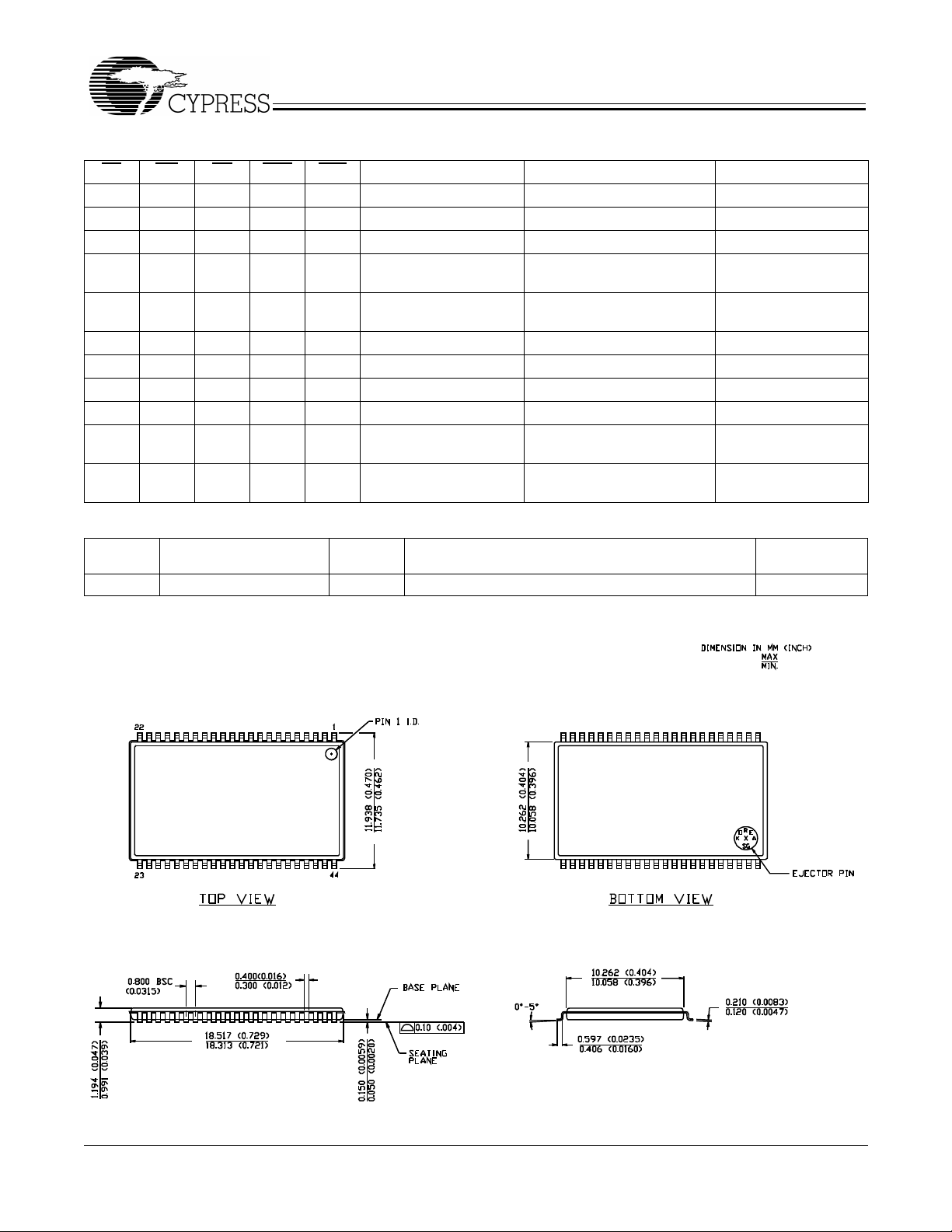
Package Diagram
44-Pin TSOP II Z44
51-85087-A
MoBL is a registered trademark, and More Battery Life is a trademark, of Cypress Semiconductor. All product and company
names mentioned in this document are the trademarks of their respective holders.
Document #: 38-05050 Rev. *A Page 8 of 9
© Cypress Semiconductor Corporation, 2002. The information contained herein is subject to change without notice. Cypress Semiconductor Corporation assumes no responsibility for the use
of any circuitry other than cir cuitry embodi ed in a Cypress S emiconductor product . Nor does it convey or imply any license un der patent or other righ ts. Cypre ss Semiconductor does not autho rize
its products for use as critical components in life-support systems where a malfunction or failure may reasonably be expected to result in significant injury to the user. The inclusion of Cypress
Semiconductor products in life-support systems application implies that the manufacturer assumes all risk of such use and in doing so indemnifies Cypress Semiconductor against all charges.
Page 9

Document Title: CY62147V MoBL® 4M (256K x 16) Static RAM
Document Number: 38-05050
REV. ECN NO. Issue Date
** 109958 12/16/01 SZV Changed from Spec number: 38-00757 to 38-05050
A 116514 09/04/02 GBI Added footnote 1.
Orig. of
Change Description of Change
Deleted fBGA package (replacement fB GA package is available in
CY62147CV30).
CY62147V MoBL
®
Document #: 38-05050 Rev. *A Page 9 of 9
 Loading...