

Datasheet CY62128LL-70ZC, CY62128LL-70SC, CY62128L-70ZC, CY62128L-70SC, CY62128-70ZC Datasheet (Cypress Semiconductor)
...Page 1
128K x 8 Static RAM
fax id: 1072
CY62128
PRELIMINARY
Cypress Semiconductor Corporation • 3901 North First Street • San Jose • CA 95134 • 408-943-2600
July 1996 - Revised November 1996
1CY62128
Features
• 4.5V − 5.5V operation
• CMOS for optimum speed/power
• Low active power (70 ns, LL version)
—330 mW (max.) (60 mA)
• Low standby power (70 ns, LL version)
—110 µW (max.) (20 µA)
• Automatic power-down when deselected
• TTL-compatible inputs and outputs
• Easy memory expansion with CE
1
, CE2, and OE options
Functional Descriptio n
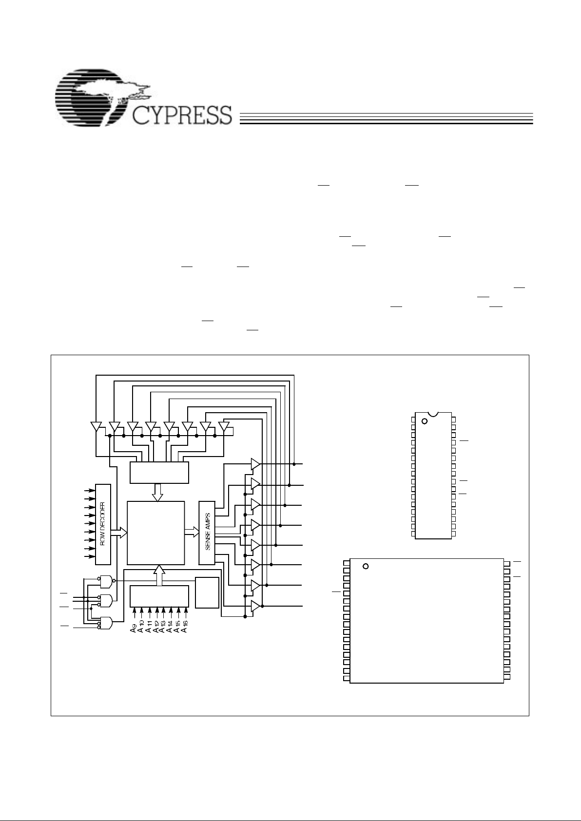
The CY62128 is a high-performance CMOS static RAM organized as 131,072 words by 8 bits. Easy memory expansion is
provided by an active LOW chip enable (CE
1
), an active HIGH
chip enable (CE
2
), an active LOW output enable (OE), a nd
three-state drivers. This device has an automatic power-down
feature that reduces power consumption by more than 75%
when deselected.
Writing to the device is accomplished by taking chip enable
one (CE
1
) and write enable (WE) inputs LOW and ch ip enable
two (CE
2
) input HIGH. Data on the eight I/O pins ( I/O0 through
I/O
7
) is then written into the location specified on the address
pins (A
0
through A16).
Reading from the device is accomplished by taking chip enable one (CE
1
) and output enable (OE) LOW while forcing
write enable (WE
) and chip enable two (CE2) HIGH. Under
these conditions, the contents of the memory location specified by the address pins will appear on the I/O pi ns.
The eight input/output pins (I/O
0
through I/O7) are placed in a
high-impedance state when the device is deselected (CE
1
HIGH or CE2 LOW), the outputs are disabled (OE HIGH), or
during a write operation (CE
1
LOW, CE2 HIGH, and WE LOW).
The CY62128 is available in a standard 400-mil-wide SOJ,
525-mil wide (450-mil-wide body width) SOIC and 32-pin
TSOP type I.
Logic Block Diagram
Pin
Configurations
A
1
A
2
A
3
A
4
A
5
A
6
A
7
A
8
COLUMN
DECODER
INPUT BUFFER
POWER
DOWN
WE
OE
I/O
0
CE
2
I/O
1
I/O
2
I/O
3
512 x 256 x 8
ARRAY
I/O
7
I/O
6
I/O
5
I/O
4
A
0
CE
1
62128-1
62128-2
1
2
3
4
5
6
7
8
9
10
11
14
19
20
24
23
22
21
25
28
27
26
T op View
SOJ / SOIC
12
13
29
32
31
30
16
151718
GND
A
16
A
14
A
12
A
7
A
6
A
5
A
4
A
3
WE
V
CC
A
15
A
13
A
8
A
9
I/O
7
I/O
6
I/O
5
I/O
4
A
2
NC
I/O
0
I/O
1
I/O
2
CE
1
OE
A
10
I/O
3
A
1
A
0
A
11
CE
2
A
6
A
7
A
16
A
14
A
12
WE
V
CC
A
4
A
13
A
8
A
9
OE
TSOP I
Top View
(not to scale)
1
6
2
3
4
5
7
32
27
31
30
29
28
26
21
25
24
23
22
19
20
I/O
2
I/O
1
GND
I/O
7
I/O
4
I/O
5
I/O
6
I/O
0
CE
1
A
11
A
5
17
18
8
9
10
11
12
13
14
15
16
CE
2
A
15
NC
A
10
I/O
3
A
1
A
0
A
3
A
2
Page 2
CY62128
2
PRELIMINARY
Maximum Ratings
(Above which the useful life may be impaired. For user guidelines, not tested.)
Storage Temperature .................................–65°C to +150°C
Ambient Temperature with
Power Applied.............................................–55°C to +125°C
Supply Voltage on V
CC
to Relative GND
[1]
.... –0.5V to +7.0V
DC Voltage Applied to Outputs
in High Z State
[1]
..................................... –0.5V to VCC +0.5V
DC Input Voltage
[1]
..................................–0.5V to VCC +0.5V
Current into Outputs (LOW) ........................................ 20 mA
Static Discharge Voltage...........................................>2001V
(per MIL-STD-883, Method 3015)
Latch-Up Current .....................................................>200 mA
Selection G uide
CY62128–55 CY62128–70
Maximum Access Time (ns) 55 70
Maximum Operating Current Commercial 115 mA 110 mA
L 70 mA 60 mA
LL 70 mA 60 mA
Maximum CMOS Standby Current Commercial 10 mA 10 mA
L 100 µA 100 µA
LL 20 µA 20 µA
Operating Range
Range
Ambient
Temperature
[2]
V
CC
Commercial 0°C to +70°C 5V ± 10%
Electrical Characteristics Over the Operating Range
[3]
62128–55 62128–70
Parameter Description Test Conditions Min. Max. Min. Max. Unit
V
OH
Output HIGH Voltage VCC = Min., IOH = – 1.0 mA 2.4 2.4 V
V
OL
Output LOW Voltage VCC = Min., IOL = 2.1mA 0.4 0.4 V
V
IH
Input HIGH Voltage 2.2 VCC+
0.3
2.2 VCC+
0.3
V
V
IL
Input LOW Voltage
[1]
–0.3 0.8 –0.3 0.8 V
I
IX
Input Load Current GND ≤ VI ≤ V
CC
–1 +1 –1 +1 µA
I
OZ
Output Leakage Current GND ≤ VI ≤ VCC, Output Disabled –5 +5 –5 +5 µA
I
OS
Output Short Circuit Current
[4]
VCC = Max., V
OUT
= GND –300 –300 mA
I
CC
VCC Operating
Supply Current
VCC = Max.
,
I
OUT
= 0 mA,
f = f
MAX
= 1/t
RC
Com’l 115 110 mA
L 70 60 mA
LL 70 60 mA
I
SB1
Automatic CE
Power-Down Current
—TTL Inputs
Max. VCC, CE1 ≥ V
IH
or CE2 < VIL,
V
IN
≥ VIH or
V
IN
≤ VIL, f = f
MAX
Com’l 25 25 mA
L 10 10 mA
LL 2 2 mA
I
SB2
Automatic CE
Power-Down Current
— CMOS Inputs
Max. VCC,
CE
1
≥ VCC – 0.3V,
or CE
2
≤ 0.3V,
V
IN
≥ VCC – 0.3V,
or V
IN
≤ 0.3V, f=0
Com’l 10 10 mA
L 100 100 µA
LL 20 20 µA
Shaded areas contain advance information
Notes:
1. V
IL
(min.) = –2.0V fo r pu lse dura tions of less tha n 20 ns.
2. TA is the “instant o n” case temper ature.
3. See the last page of this specification for Group A subgroup testing information.
4. Not more than one output should be shorted at one time. Duration of the short circuit should not exceed 30 seconds.
Page 3
CY62128
3
PRELIMINARY
Capacitance
[5]
Parameter Description Test Conditions Max. Unit
C
IN
Input Capacitance TA = 25°C, f = 1 MHz,
V
CC
= 5.0V
9 pF
C
OUT
Output Capacitance 9 pF
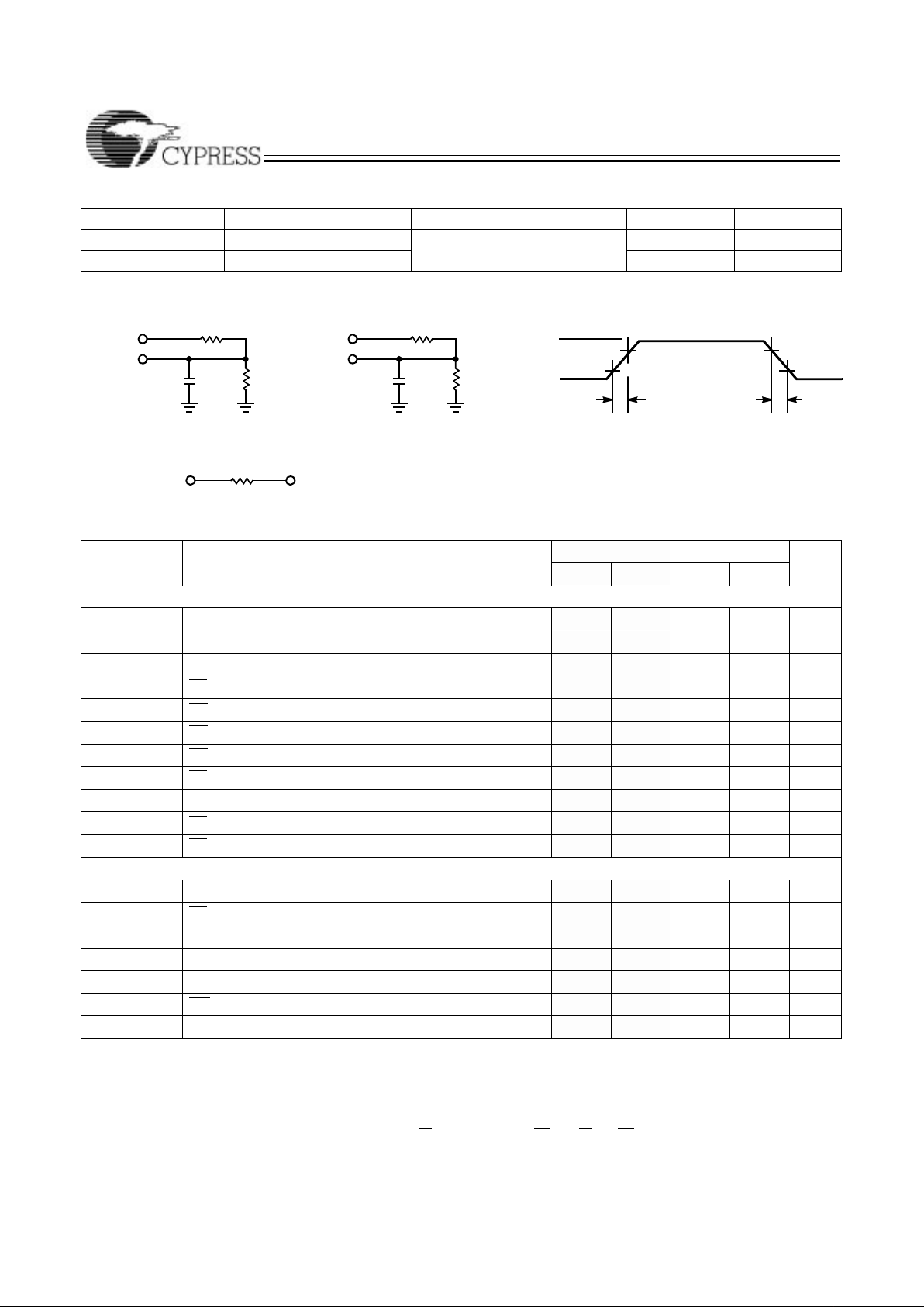
AC Test Loads and Waveforms
Switching Characteristics
[3,6]
Over the Operating Range
62128–55 62128–70
Parameter Description Min. Max. Min. Max. Unit
READ CYCLE
t
RC
Read Cycle Time 55 70 ns
t
AA
Address to Data Valid 55 70 ns
t
OHA
Data Hold from Address Change 5 5 ns
t
ACE
CE1 LOW to Data Valid, CE2 HIGH to Data Valid 55 70 ns
t
DOE
OE LOW to Data Valid 20 35 ns
t
LZOE
OE LOW to Low Z 0 0 ns
t
HZOE
OE HIGH to High Z
[7, 8]
20 25 ns
t
LZCE
CE1 LOW to Low Z, CE2 HIGH to Low Z
[8]
5 5 ns
t
HZCE
CE1 HIGH to High Z, CE2 LOW to High Z
[7, 8]
20 25 ns
t
PU
CE1 LOW to Power-Up, CE2 HIGH to Power-Up 0 0 ns
t
PD
CE1 HIGH to Power-Down, CE2 LOW to Power-Down 55 70 ns
WRITE CYCLE
[9]
t
WC
Write Cycle Time 55 70 ns
t
SCE
CE1 LOW to Write End, C E2 HIGH to Write End 45 60 ns
t
AW
Address Set-Up to Write End 45 60 ns
t
HA
Addre ss H old from Write End 0 0 ns
t
SA
Address Set-Up to Write Start 0 0 ns
t
PWE
WE Pulse Width 45 50 ns
t
SD
Data Set-Up to Write End 45 55 ns
Shaded areas contain advance information
Notes:
5. Tested initially and after any design or process changes that may affect these parameters.
6. Test conditions assume signal transition time of 5ns or less, timing reference levels of 1.5V, input pulse levels of 0 to 3.0V, and output loading of the specified
I
OL/IOH
and 100pF load capaci tance.
7. t
HZOE
, t
HZCE
, and t
HZWE
are specified with a load capa citance of 5 pF as i n part ( b) of A C Test Loads. T ran sition is meas ured ±500 mV fr om steady- state v oltag e.
8. At any given temperature and voltage condition, t
HZCE
is less than t
LZCE
, t
HZOE
is less tha n t
LZOE
, and t
HZWE
is less than t
LZWE
for any given dev ice.
9. The internal write time of the memory is defined by the overlap of CE
1
LOW, C E2 HIGH, and WE LOW . CE1 and WE must be LO W and CE2 HIGH to initiate a write,
and the transition of an y of th ese s ignals can te rminate the write. T he inp ut dat a set- up a nd hold timing s hould be r eferenced t o th e leadi ng edge o f the s ignal that ter minates
the write.
62128-3
62128-4
90%
10%
3.0V
GND
90%
10%
ALL INPUT PULSES
5V
OUTPUT
100 pF
INCLUDING
JIG AND
SCOPE
5V
OUTPUT
5 pF
INCLUDING
JIG AND
SCOPE
(a)
(b)
≤ 5ns ≤ 5ns
OUTPUT
R1 1800
Ω
R1 1800 Ω
R2
990Ω
R2
990Ω
639Ω
Equivalent to: THÉVENIN EQUIVALENT
1.77V
Page 4

CY62128
4
PRELIMINARY
t
HD
Data Hold from Write E nd 0 0 ns
t
LZWE
WE HIGH to Low Z
[8]
5 5 ns
t
HZWE
WE LOW to High Z
[7,8]
20 25 ns
Shaded area contains advanced information.
Switching Characteristics
[3,6]
Over the Operating Range (continued)
62128–55 62128–70
Parameter Description Min. Max. Min. Max. Unit
Switching Waveforms
Read Cycle No.1
[10,11]
Read Cycle No. 2 (OE Controlled)
[11,12]
Notes:
10. Device is continuously selected. OE
, CE1 = VIL, CE2 = VIH.
11. WE is HIGH for read cy cle.
12. Address valid prior to or coincident with CE1 transition LOW an d CE2 transition HIG H.
PREVIOUS DATA VALID DATA VALID
t
RC
t
AA
t
OHA
62128-5
ADDRESS
DATA OUT
62128-6
50%
50%
DATA VALID
t
RC
t
ACE
t
DOE
t
LZOE
t
LZCE
t
PU
HIGH IMPEDANCE
t
HZOE
t
HZCE
t
PD
HIGH
OE
CE
1
ICC
ISB
IMPEDANCE
ADDRESS
CE
2
DATA OUT
V
CC
SUPPLY
CURRENT
Page 5

CY62128
5
PRELIMINARY
Write Cycle No. 1 (CE1 or CE2 Controlled)
[13,14]
Write Cycle No. 2 (WE Controlled, OE HIGH During Write)
[13,14]
Notes:
13. Data I/O is high impedance if OE
= VIH.
14. If CE
1
goes HIGH or CE2 goes LOW simultaneo usly wit h WE going H IGH, t he out put remai ns in a hi gh-impedanc e state.
15. During this period the I/Os are in the output state and input signals should not be applied.
Switching Waveforms (continued)
62128-7
t
WC
DATA VALID
t
AW
t
SA
t
PWE
t
HA
t
HD
t
SD
t
SCE
t
SCE
CE
1
ADDRESS
CE
2
WE
DATA I/O
62128-8
t
HD
t
SD
t
PWE
t
SA
t
HA
t
AW
t
SCE
t
SCE
t
WC
t
HZOE
DATAINVALID
CE
1
ADDRESS
CE
2
WE
DATA I/O
OE
NOTE15
Page 6

CY62128
6
PRELIMINARY
Document #: 38–00524
Write Cycle No.3 (WE Controlled, OE LOW)
[13,14]
Switching Waveforms (continued)
62128-9
DATA VALID
t
HD
t
SD
t
LZWE
t
PWE
t
SA
t
HA
t
AW
t
SCE
t
SCE
t
WC
t
HZWE
CE
1
ADDRESS
CE
2
WE
DATAI/O
NOTE 15
Truth Table
CE1CE2OE WE I/O0 – I/O
7
Mode Power
H X X X High Z Power-Down Standby (ISB)
X L X X High Z Power-Down Standby (ISB)
L H L H Data Out Read Active (ICC)
L H X L Data In Write Active (ICC)
L H H H High Z Selected, Outputs Disabled Active (ICC)
Ordering Info rma tio n
Speed
(ns) Ordering Code
Package
Name Package Type
Operating
Range
55 CY62128–55VC V33 3 2 -Lead (400-Mil) Molded SO J Commercial
CY62128–55SC S34 32-Lead (450-Mil) M ol ded SOIC
CY62128−55ZC Z32 32-Lead TSOP TypeI
70 CY62128–70VC V33 3 2 -Lead (400-Mil) Molded SO J Commercial
CY62128–70SC S34 32-Lead (450-Mil) M ol ded SOIC
CY62128−70ZC Z32 32-Lead TSOP Type I
CY62128L−70SC S34 32-Lead (450-Mil) Molded SOIC
CY62128L−70ZC Z32 32-Lead TSOP Type I
CY62128LL−70SC S34 32-Lead (450-Mil) Molded SOIC
CY62128LL−70ZC Z32 32-Lead TSOP Type I
Shaded area contains advanced information.
Page 7

CY62128
7
PRELIMINARY
Package Diagrams
32- Le ad (450 Mil) Molded SOIC S34
32-Lead Thin Small Outline Package Z32
Page 8

CY62128
PRELIMINARY
© Cypress Semiconductor Cor p oration, 1996. The information contained herein is subject to change without notice. Cypress Semiconductor Corporation assumes no responsibility for the use
of any circuitry othe r than circui try embodi ed in a Cypress Semi conductor p roduct. Nor does it convey or imply any licens e under patent or other rights. Cypress Semi conductor does not authori ze
its products for use as critical components in life-support systems where a malfunction or failure may reasonably be expected to result in significant injury to the user. The inclusion of Cypress
Semiconductor products in life-support systems application implies that the manufacturer assumes all risk of such use and in doing so indemnifies Cypress Semiconductor again st all charges.
Package Diagrams (continued)
32-Lead (400-Mil) Molded SOJ V33
 Loading...