

Page 1

CXP83232A/83240A
CMOS 8-bit Single Chip Microcomputer
Description
The CXP83232A/83240A is a CMOS 8-bit single
chip microcomputer integrating on a single chip an
A/D converter, serial interface, timer/counter, time
base timer, 32kHz timer/counter, capture timer
counter, LCD controller/driver, remote control
reception circuit and 14-bit PWM output besides the
basic configurations of 8-bit CPU, ROM, RAM, and
I/O port.
The CXP83232A/83240A also provides a sleep/stop
function that enables lower power consumption.
Features
• Wide-range instruction system (213 instructions) to cover various types of data.
— 16-bit arithmetic/multiplication and division/boolean bit operation instructions
• Minimum instruction cycle 400ns at 10MHz operation
8µs at 500kHz
122µs at 32kHz operation
• Incorporated ROM capacity 32Kbytes (CXP83232A)
40Kbytes (CXP83240A)
• Incorporated RAM capacity 1120bytes (includes LCD display data area)
• Peripheral functions
— A/D converter 8-bit, 8-channel, successive approximation method
(Conversion time of 32µs/10MHz)
— Serial interface 8-bit, 8-stage FIFO incorporated
(Auto transfer for 1 to 8 bytes), 1 channel
8-bit clock synchronized type, 1 channel
— Timer 8-bit timer, 8-bit timer/counter, 19-bit time base timer,
16-bit capture timer/counter, 32kHz timer/counter
— LCD controller/driver Maximum 160 segment display possible (during 1/4 duty)
4 common output, 40 segment output
Display method static, 1/2, 1/3, 1/4 duty
Bias method 1/2, 1/3 bias
— Remote control reception circuit 8-bit pulse measuring counter, 6-stage FIFO
— PWM output circuit 14 bits, 1 channel
• Interruption 15 factors, 15 vectors, multi-interruption possible
• Standby mode SLEEP/STOP
• Package 100-pin plastic QFP/LQFP
• Piggyback/evaluation chip CXP83200A 100-pin ceramic QFP/LQFP
100 pin QFP (Plastic) 100 pin LQFP (Plastic)
Structure
Silicon gate CMOS IC
Sony reserves the right to change products and specifications without prior notice. This information does not convey any license by
any implication or otherwise under any patents or other right. Application circuits shown, if any, are typical examples illustrating the
operation of the devices. Sony cannot assume responsibility for any problems arising out of the use of these circuits.
– 1 –
E94842-PP
Page 2
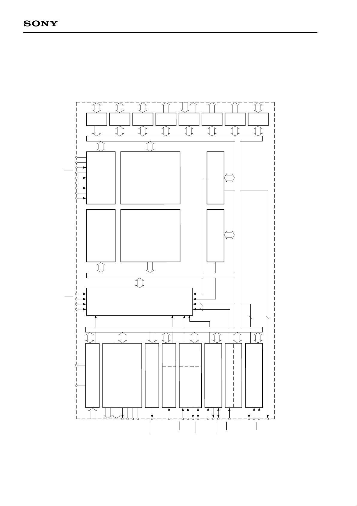
CXP83232A/83240A
SS
DD
V
V
RST
XTAL1
EXTAL1
XTAL2
EXTAL2
TX
TEX
PA0 to PA7
8
CLOCK GEN/
SPC 700
PORT A
SYSTEM CONTROL
CPU CORE
PB0 to PB7
8
PC0 to PC7
8
PORT B
PD0 to PD7
8
PORT C
RAM
PE0 to PE4
PE5 to PE6
5
2
PORT D
PF0 to PF7
8
PORT E
PG0 to PG7
8
PORT F
PH0 to PH7
8
PORT G
PORT H
32KHz
1120 BYTES
TIMER/COUNTER
ROM
32K/40K BYTES
PRESCALER/
TIME BASE TIMER
Block Diagram
REF
SS
NMI/INT3
INT2
INT1
INT0
AV
AV
INTERRUP T CONTROLLER
2 2
2
2
FIFOREMOCON
LCD
DRIVER
A/D CONVERT ER
CONTROLLER/
1 4 B IT PWM G ENERATO R
8
4
40
VL
VLC1
VLC2
VLC3
RMC
PWM
FIFO
8 BIT TI ME R 1
TO
16 BIT CAPTURE
TIMER/COUNTER 2
EC1
ADJ
CINT
UNIT 0
SERIAL
INTERFACE
SI0
CS0
SI1
SO0
SCK0
8 BIT T IMER/ COUNTE R 0
SERIAL INTERFACE UNIT 1
SO1
EC0
SCK1
AN0 to AN7
SEG0 to SEG39
COM0 to COM3
– 2 –
Page 3

Pin Assignment (Top View) (QFP package)
SEG38/PG6
SEG37/PG5
SEG39/PG7
PE1/INT1/EC1
100
99
PE0/INT0/EC0
98
97
96
SEG36/PG4
95
TEX
SEG35/PG3
93
94
92
TX
91
CXP83232A/83240A
SS
DD
SEG33/PG1
V
90
NC
V
89
SEG34/PG2
88
87
SEG31/PF7
SEG32/PG0
86
85
SEG29/PF5
SEG30/PF6
84
83
SEG27/PF3
SEG28/PF4
81
82
PE3/INT2
PE3/INT3/NMI
PE4/RMC
PE5/PWM
PE6/TO/ADJ
PB0/CINT
PB1/CS0
PB2/SCK0
PB3/SI0
PB4/SO0
PB5/SCK1
PB6/SI1
PB7/SO1
PC0
PC1
PC2
PC3
PC4
PC5
PC6
PC7
PH0
PH1
PH2
PH3
PH4
PH5
PH6
PH7
PA0/AN0
10
15
16
17
18
19
20
29
30
11
12
13
14
21
22
23
24
25
26
27
28
1
2
3
4
5
6
7
8
9
35
31
32
33
34
36
37
38
39
40
41
42
43
44
45
46
47
48
49
50
80
78
77
76
75
74
69
68
67
66
65
64
63
62
60
59
58
57
56
55
54
53
52
51
79
73
72
71
70
61
SEG26/PF2
SEG25/PF1
SEG24/PF0
SEG23/PD7
SEG22/PD6
SEG21/PD5
SEG20/PD4
SEG19/PD3
SEG18/PD2
SEG17/PD1
SEG16/PD0
SEG15
SEG14
SEG13
SEG12
SEG11
SEG10
SEG9
SEG8
SEG7
SEG6
SEG5
SEG4
SEG3
SEG2
SEG1
SEG0
COM3
COM2
COM1
PA2/AN2
PA1/AN1
PA4/AN4
PA3/AN3
PA6/AN6
PA5/AN5
RST
PA7/AN7
XTAL1
EXTAL1
SS
V
XTAL2
REF
AV
EXTAL2
SS
AV
Note) 1. NC (Pin 90) is always connected to VDD.
2. VSS (Pin 41 and 91) are both connected to GND.
– 3 –
L
V
LC3VLC2
V
LC1
V
COM0
Page 4

Pin Assignment (Top View) (LQFP package)
SEG39/PG7
PE0/INT0/EC0
96
95
SEG38/PG6
SEG36/PG4
SEG37/PG5
93
94
92
PE4/RMC
PE5/PWM
PE6/TO/ADJ
PB0/CINT
PB1/CS0
PB2/SCK0
PB3/SI0
PB4/SO0
PB5/SCK1
PB6/SI1
PB7/SO1
PC0
PC1
PC2
PC3
PC4
PC5
PC6
PC7
PH0
PH1
PH2
PH3
PH4
PH5
PE3/INT3/NMI
100
1
2
3
4
5
6
7
8
9
10
11
12
13
14
15
16
17
18
19
20
21
22
23
24
25
PE1/INT1/EC1
PE2/INT2
99
98
97
TX
SEG35/PG3
TEX
89
91
90
CXP83232A/83240A
DD
SS
NC
V
88
87
SEG34/PG2
V
86
SEG33/PG1
SEG32/PG0
84
83
85
SEG29/PF5
SEG31/PF7
SEG30/PF6
81
82
SEG28/PF4
SEG27/PF3
80
79
SEG25/PF1
SEG26/PF2
78
77
SEG24/PF0
76
75
74
73
72
71
70
69
68
67
66
65
64
63
62
61
60
59
58
57
56
55
54
53
52
51
SEG23/PD7
SEG22/PD6
SEG21/PD5
SEG20/PD4
SEG19/PD3
SEG18/PD2
SEG17/PD1
SEG16/PD0
SEG15
SEG14
SEG13
SEG12
SEG11
SEG10
SEG9
SEG8
SEG7
SEG6
SEG5
SEG4
SEG3
SEG2
SEG1
SEG0
COM3
26
27
PH6
28
PH7
30
29
PA1/AN1
PA0/AN0
32
31
PA3/AN3
PA2/AN2
33
34
PA5/AN5
PA4/AN4
36
PA6/AN6
PA7/AN7
37
RST
EXTAL1
38
XTAL1
39
SS
V
40
XTAL2
41
35
Note) 1. NC (Pin 88) is always connected to VDD.
2. VSS (Pin 39 and 89) are both connected to GND.
– 4 –
43
42
REF
AV
EXTAL2
SS
AV
44
46
45
L
V
LC2
LC3
V
V
47
LC1
V
48
49
COM0
50
COM2
COM1
Page 5
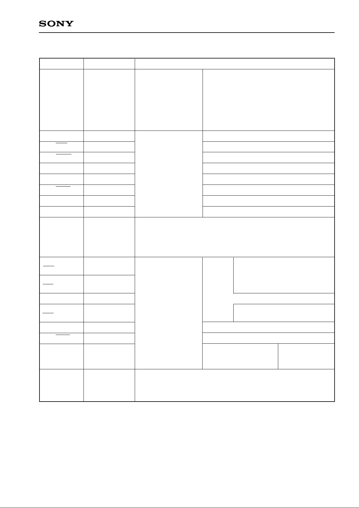
Pin Description
Symbol I/O Functions
(Port A)
8-bit I/O port. I/O can
PA0/AN0
to
PA7/AN7
I/O/Analog input
be set in a single bit
unit.
Incorporation of pull-up
resistor can be set
Analog inputs to A/D converter.
(8 pins)
through the software in
a unit of 4 bits. (8 pins)
CXP83232A/83240A
PB0/CINT
PB1/CS0
PB2/SCK0
PB3/SI0
PB4/SO0
PB5/SCK1
PB6/SI1
PB7/SO1
PE0/INT0/
EC0
PE1/INT1/
EC1
PE2/INT2
PE3/INT3/
NMI
PE4/RMC
I/O/Input
I/O/Input
I/O/I/O
I/O/Input
I/O/Output
I/O/I/O
I/O/input
I/O/Output
I/OPC0 to PC7
Input/Input/Input
Input/Input/Input
Input/Input
Input/Input/Input
Input/Input
External capture input to 16-bit timer/counter.
(Port B)
Chip select input for serial interface (CH0).
8-bit I/O port. I/O can
be set in a single bit
unit.
Serial clock I/O (CH0).
Serial data input (CH0).
Incorporation of pull-up
resistor can be set
through the software in
Serial data output (CH0).
Serial clock I/O (CH1).
a unit of 4 bits.
(8 pins)
Serial data input (CH1).
Serial data output (CH1).
(Port C)
8-bit I/O port. I/O can be set in a single bit unit. Capable of driving 12mA
sync current. Incorporation of pull-up resistor can be set through the
software in a unit of 4 bits.
(8 pins)
External event inputs for
timer/counter.
(2 pins)
(Port E)
7-bit port. lower 5 bits
are for inputs; upper 2
bits are for outputs.
(7 pins)
External interruption request inputs.
(4 pins)
Non-maskable interruption request
input.
Remote control reception circuit input.
PE5/PWM
PE6/TO/
ADJ
PH0 to PH7
Output/Output
Output/Output/
Output
I/O
14-bit PWM output.
Rectangular wave output
for 16-bit timer/counter
(duty output 50%).
Output for 32kHz
oscillation
frequency division.
(Port H)
8-bit I/O port. I/O can be set in a single bit unit. Incorporation of pull-up
resistor can be set through the software in a unit of 4 bits.
(8 pins)
– 5 –
Page 6
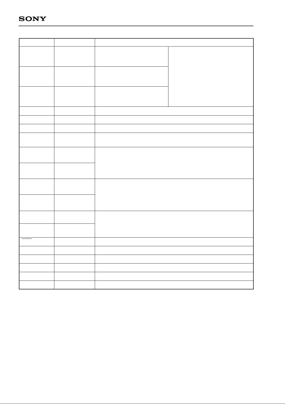
Symbol I/O Functions
PD0/SEG16
to
PD7/SEG23
Output/Output
(Port D)
8-bit output port.
(8 pins)
CXP83232A/83240A
PF0/SEG24
to
PF7/SEG31
PG0/SEG32
to
PG7/SEG39
SEG0 to SEG15
COM0 to COM3
Output/Output
Output/Output
Output
Output
(Port F)
8-bit output port.
(8 pins)
(port G)
8-bit output port.
(8 pins)
LCD segment signal output.
LCD common signal output.
VLC1 to VLC3 LCD bias power supply.
VL
EXTAL1
Output
Input
Control pin to cut off the current flowing to external LCD bias resistor
during standby.
Crystal connectors for system clock oscillation. When the clock is supplied
externally, input to EXTAL1; opposite phase clock should be input to XTAL1.
System clock oscillation of EXTAL1 and XTAL1 is used for normal operation
XTAL1
EXTAL2
Input
mode (Max. 10MHz).
Crystal connectors for system clock oscillation. When the clock is supplied
externally, input to EXTAL2; opposite phase clock should be input to XTAL2.
System clock oscillation of EXTAL2 and XTAL2 is used for sub clock mode
XTAL2
(Typ. 500kHz).
LCD segment signal output.
TEX
RST
NC
AVREF
AVSS
VDD
VSS
Input
OutputTX
Input
Input
Crystal connectors for 32kHz timer/counter clock generation circuit.
Connect a 32.768kHz crystal oscillator between TEX and TX. For usage
as event input, connect clock oscillation source to TEX, and leave TX
open.
Low-level active system reset.
NC. Under normal operating conditions, connect to VDD.
Reference voltage input for A/D converter.
A/D converter GND.
Positive power supply.
GND. Two VSS are connected to GND.
– 6 –
Page 7
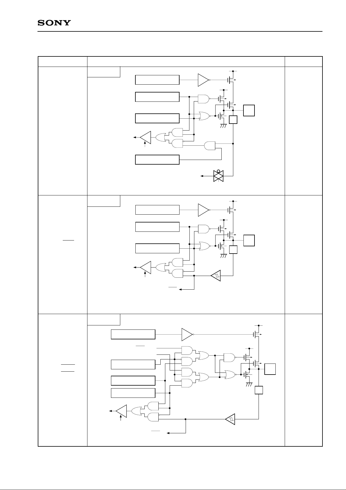
I/O Circuit Format for Pins
CXP83232A/83240A
Pin
PA0/AN0
to
PA7/AN7
8 pins
Port A
Port B
Data bus
Pull-up resistor
"0" when reset
Port A data
Port A direction
"0" when reset
RD (Port A)
Port A input selection
"0" when reset
Pull-up resistor
"0" when reset
Port B data
Circuit format
Input multiplexer
A/D converter
∗
Input protection
IP
circuit
∗ Pull-up transistors
approx. 100kΩ
∗
When reset
Hi-Z
PB0/CINT
PB1/CS0
PB3/SI0
PB6/SI1
4 pins
PB2/SCK0
PB5/SCK1
Port B
Data
bus
Port B direction
"0" when reset
Data bus
RD (Port B)
Pull-up resistor
"0" when reset
SCK OUT
Output enable
Port B output selection
"0" when reset
Port B data
Port B direction
"0" when reset
CINT
CS0
SI0
SI1
IP
Hi-Z
Schmitt input
∗ Pull-up transistors
approx. 100kΩ
∗
Hi-Z
IP
Schmitt input
RD (Port B)
SCK in
∗ Pull-up transistors
approx. 100kΩ
– 7 –
Page 8
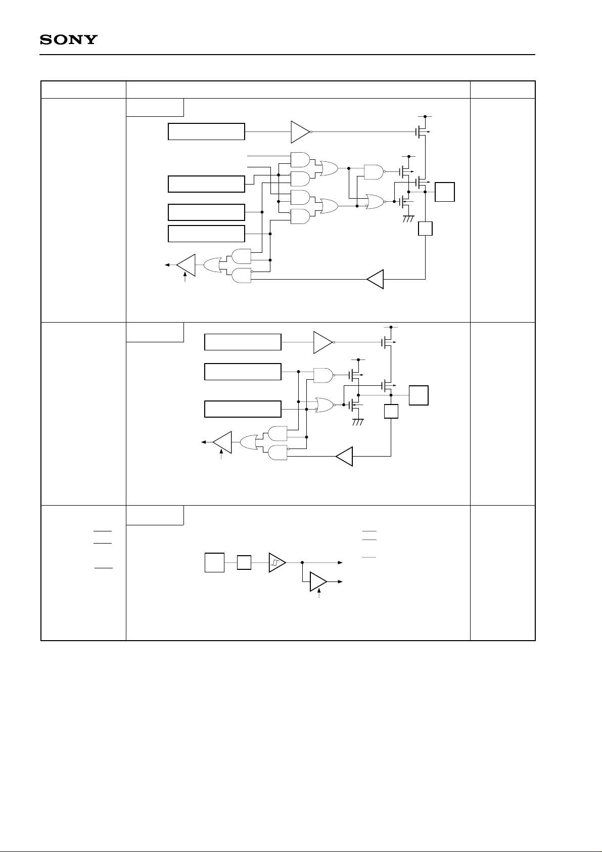
CXP83232A/83240A
Pin
PB4/SO0
PB7/SO1
2 pins
Port B
Data
bus
Port C
Pull-up resistor
"0" when reset
Output enable
Port B output selection
"0" when reset
Port B data
Port B direction
"0" when reset
RD (Port B)
SO
Pull-up resistor
"0" when reset
Port C data
Circuit format
∗ Pull-up transistors
approx. 100kΩ
∗
2
When reset
∗
Hi-Z
IP
PC0 to PC7
8 pins
PE0/INT0/EC0
PE1/INT1/EC1
PE2/INT2
PE3/INT3/NMI
PE4/RMC
5 pins
Port E
Data bus
Port C direction
"0" when reset
RD (Port C)
Schmitt input
IP
RD (Port E)
∗1
IP
∗
1
High current drive
of 12mA possible
∗
2
Pull-up transistors
approx. 100k Ω
INT0/EC0
INT1/EC1
INT2
INT3/NMI
RMC
Data bus
Hi-Z
Hi-Z
– 8 –
Page 9

CXP83232A/83240A
Pin
PE5/PWM
1 pin
PE6/TO/ADJ
1 pin
Port E
Data bus
Port E
Port E data
"1" when reset
∗
Port E output selection
Port E output selection
"00" when reset
TO Output enable
Port E output selection
"0" when reset
Reset E data
RD (Port E)
TO
2
ADJ16K
ADJ2K
Circuit format
PWM
"1" when reset
Internal reset signal
MPX
∗1
∗2
∗
1
Pull-up transistors approx. 150kΩ.
ADJ signals are frequency divider outputs for
32kHz oscillation frequency adjustment.
ADJ2K provides usage as buzzer output.
When reset
High level
High level
(High level
with 150kΩ
resistor
when reset)
PH0 to PH7
8 pins
Port H
Data bus
Pull-up resistor
"0" when reset
Port H data
Port H direction
"0" when reset
RD (Port H)
∗
Hi-Z
IP
∗ Pull-up transistors approx. 100kΩ
– 9 –
Page 10
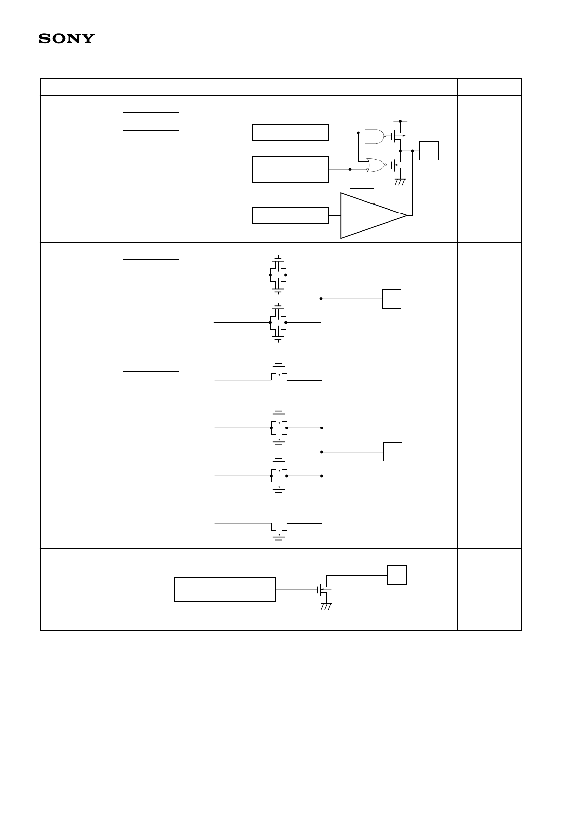
CXP83232A/83240A
Pin
PD0 to PD7
PF0 to PF7
PG0 to PG7
24pins
SEG0 to
SEG15
16 pins
Port D
Port F
Port G
PD7 to PD4
PD3 to PD0
PF7 to PF0
PG7 to PG0
Segment
Common
by a single bit unit
by 4-bit unit
by 8-bit unit
VCH
VCL
VDD
Circuit format
Port data
Port/segment output
selection
"0" when reset
Segment data
When reset
Segment
output
(VDD level)
Segment
driver
VDD level
COM0 to
COM3
4 pins
VL
1 pin
VLC1
VLC2
VLC3
LCD control
(DSP bit)
"0" when reset
VDD level
Hi-Z
– 10 –
Page 11
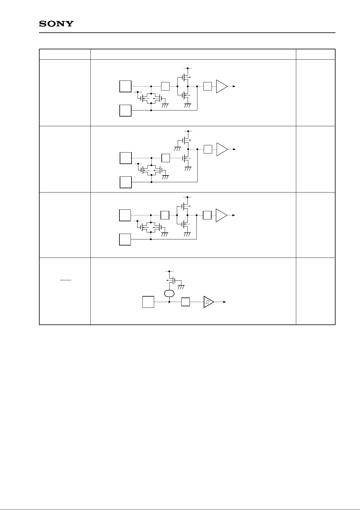
CXP83232A/83240A
Pin
EXTAL1
XTAL1
2 pins
EXTAL2
XTAL2
2 pins
TEX
TX
2 pins
EXTAL1
XTAL1
EXTAL2
XTAL2
TEX
TX
Circuit format
IP
• Diagram shows circuit
IPIP
IP
IPIP
• When the operation of the oscillation
circuit is stopped by the software, the
feedback resistor is removed and TEX
and TX become "Low" level and "High"
level respectively.
composition during
oscillation.
• Feedback resistor is
removed during stop.
XTAL1 becomes "High"
level.
• Diagram shows circuit
composition during
oscillation.
• Feedback resistor is
removed during stop.
XTAL2 becomes "High"
level.
• Diagram shows circuit
composition during
oscillation.
When reset
Oscillation
EXTAL2
Hi-Z
XTAL2
High level
Oscillation
RST
1 pin
OP
Pull-up resistor
Mask option
IP
Low level
Schmitt input
– 11 –
Page 12

CXP83232A/83240A
Absolute Maximum Ratings (Vss = 0V)
Item Symbol Rating Unit Remarks
Supply voltage
LCD bias voltage
Input voltage
Output voltage
High level output current
High level total output current
VDD
AVSS
VLC1, VLC2, VLC3
VIN
VOUT
IOH
∑IOH
IOL
–0.3 to +7.0
–0.3 to +0.3
–0.3 to +7.0
–0.3 to +7.0
–0.3 to +7.0
–5
–50
15
∗1
∗1
∗1
V
V
V
V
V
mA
Output per pin
mA
Total for all output pins
mA
Value per pin, excluding high current outputs
Low level output current
20
100
–20 to +75
–55 to +150
Low level total output current
Operating temperature
Storage temperature
IOLC
∑IOL
Topr
Tstg
600
Allowable power dissipation
PD
380
∗1
VIN and VOUT must not exceed VDD + 0.3V.
∗2
The high current drive transistor is the N-ch transistor of Port C (PC)
mA
mA
°C
°C
mW
Value per pin∗2for high current outputs
Total for all output pins
QFP package
LQFP package
Note) Usage exceeding absolute maximum ratings may permanently impair the LSI. Normal operation should
be conducted under the recommended operating conditions. Exceeding these conditions may
adversely affect the reliability of the LSI.
– 12 –
Page 13
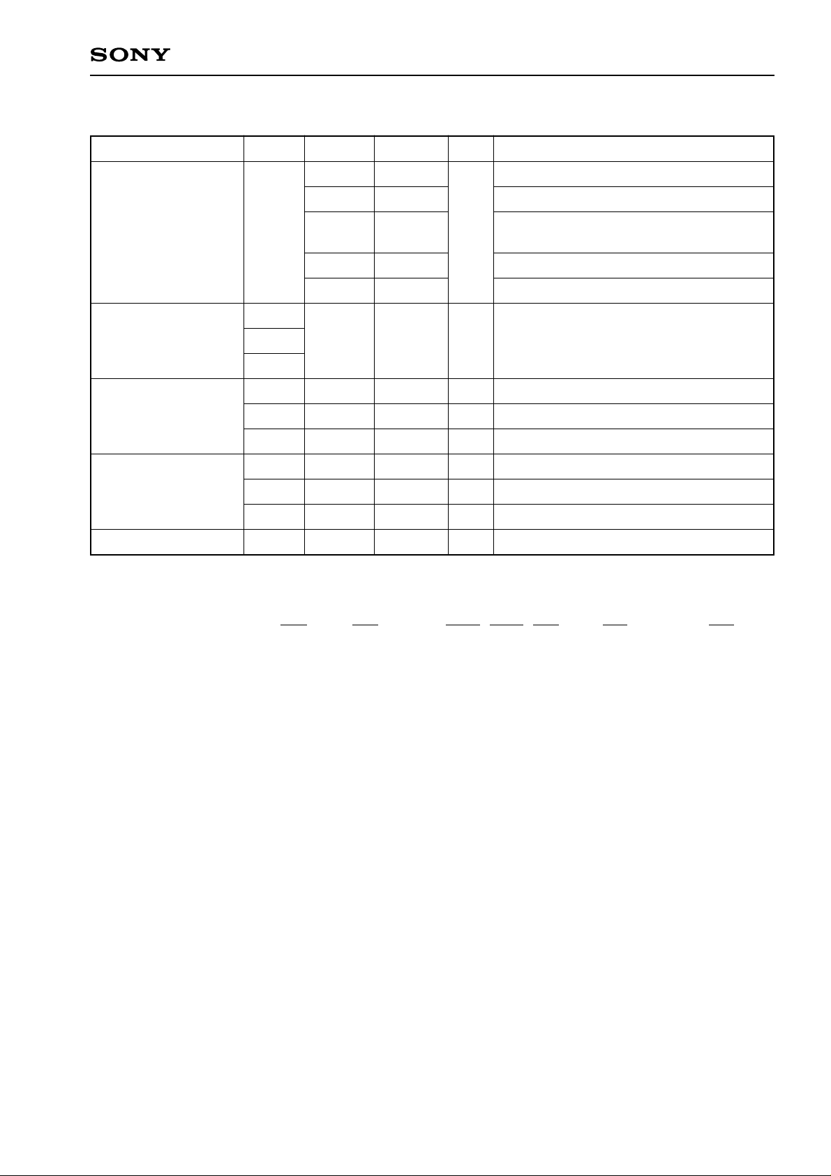
CXP83232A/83240A
Recommended Operating Conditions (Vss = 0V)
Item Symbol Min. Max. Unit Remarks
4.5
3.5
5.5
5.5
High-speed mode guaranteed operation range
Low-speed mode guaranteed operation range
∗1
∗1
Supply voltage
VDD
3.0
2.7
2.5
5.5
5.5
5.5
Guaranteed operation range during
V
EXTAL2 clock (sub clock mode)
Guaranteed operation range with TEX clock
Guaranteed data hold range during STOP
VLC1
LCD bias voltage
VLC2
Vss
VDD
V
LCD power supply range
∗5
VLC3
VIH
High level
input voltage
VIHS
VIHEX
VIL
Low level
input voltage
VILS
VILEX
Operating temperature
∗1
During EXTAL1 clock (main clock mode), high-speed mode is 1/2 frequency division clock selection; low-
Topr
0.7VDD
0.8VDD
VDD – 0.4
0
0
–0.3
–20
VDD
VDD
VDD + 0.3
0.3VDD
0.2VDD
0.4
+75
∗2
V
V
Hysteresis input
V
EXTAL
∗2
V
V
Hysteresis input
V
EXTAL
°C
∗3
∗4
∗3
∗4
speed mode is 1/16 frequency division clock selection.
∗2
Value for each pin of normal input ports (PA, PB4, PB7, PC and PH).
∗3
Value of the following pins; RST, CINT CS0, SI0, SI1, SCK0, SCK1, EC0/INT0, EC1/INT1, INT2, NMI/INT3,
and RMC.
∗4
Specifies only during external clock input.
∗5
Optimal values are determined by LCD used.
– 13 –
Page 14
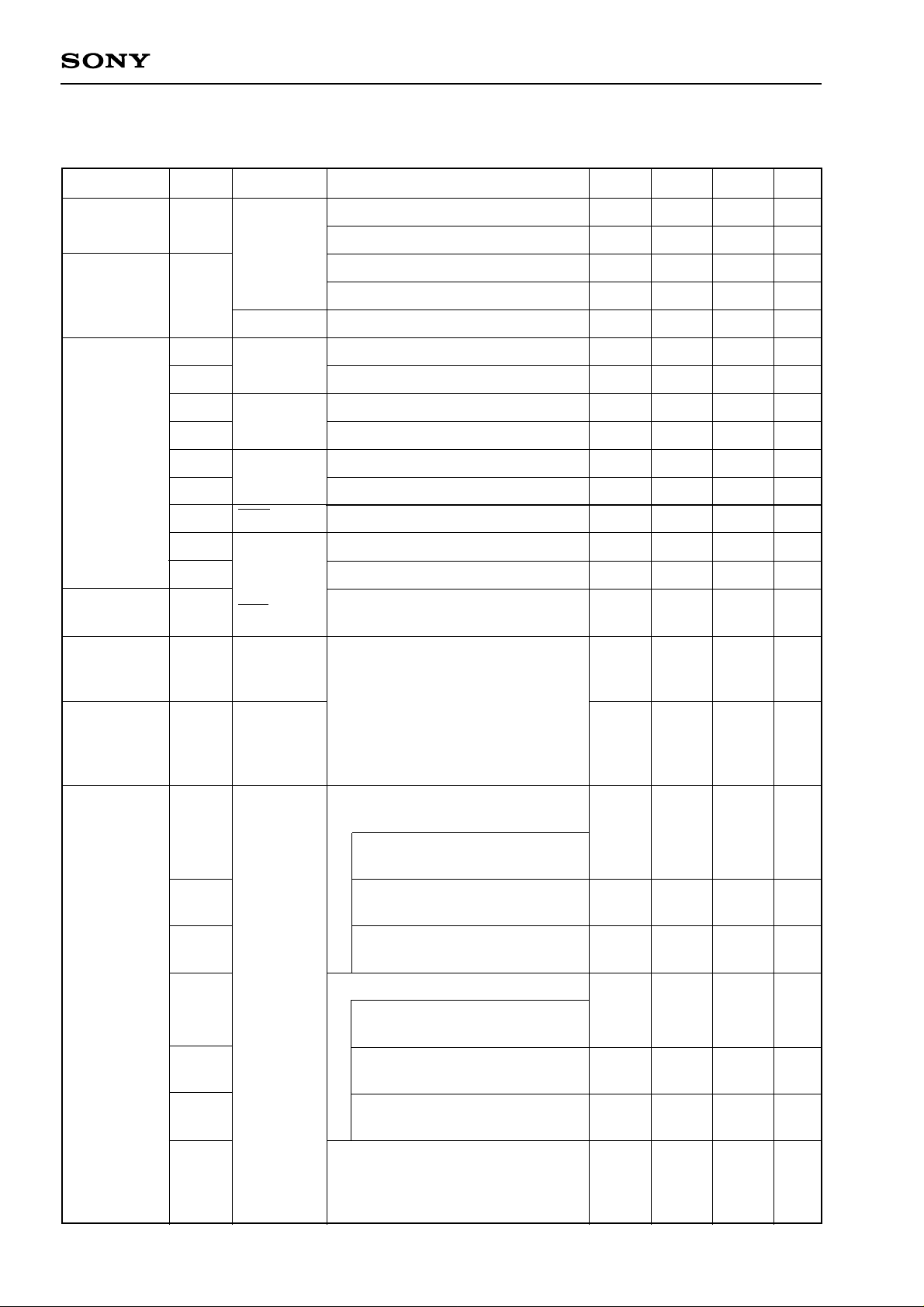
Electrical Characteristics
DC Characteristics
CXP83232A/83240A
(Ta = –20 to +75°C, Vss = 0V)
Item Symbol Pins Conditions Min.
High level
output voltage
VOH
PA, PB, PC,
PD∗1, PE5,
VDD = 4.5V, IOH = –0.5mA
VDD = 4.5V, IOH = –1.2mA
PE6
VDD = 4.5V, IOL = 1.8mA
∗3
∗2
∗2
∗1
VDD = 4.5V, IOL = 3.6mA
VDD = 4.5V, IOL = 12.0mA
VDD = 5.5V, VIH = 5.5V
VDD = 5.5V, VIL = 0.4V
VDD = 5.5V, VIH = 5.5V
VDD = 5.5V, VIL = 0.4V
VDD = 5.5V, VIH = 5.5V
VDD = 5.5V, VIL = 0.4V
VDD = 5.5V, VIL = 0.4V
VDD = 4.5V, VIH = 4.0V
VDD = 5.5V, VIL = 0.4V
VDD = 5.5V,
VI = 0, 5.5V
Low level
output voltage
Input current
I/O leakage
current
VOL
IIHE1
IILE1
IIHE2
IILE2
IIHT
IILT
IILR
IIH
IIL
IIZ
PF to PG
VL (only VOL)
PC
EXTAL1
EXTAL2
TEX
RST
PA to PC∗3,
PH
PE0 to PE4,
RST
4.0
3.5
0.5
–0.5
0.3
–0.3
0.1
–0.1
–1.5
–3.33
Typ.
Max. Unit
V
V
0.4
0.6
1.5
40
–40
30
–30
10
–10
–400
V
V
V
µA
µA
µA
µA
µA
µA
µA
µA
–50
±10
µA
µA
Common
output
impedance
Segment
output
impedance
Supply
current
∗4
RCOM
RSEG
IDD1
IDD2
IDD3
IDDS1
IDDS2
COM0 to
COM3
SEG0 to
SEG15
SEG16 to
SEG39
VDD
VDD = 5V,
VLC1 = 3.75V
VLC2 = 2.5V
VLC3 = 1.25
∗1
High-speed mode operation
(1/2 frequency division clock)
VDD = 5.5V, 10MHz crystal oscillation
(C1 = C2 = 15pF)
VDD = 3.5V, 500kHz crystal oscillation
(C1 = C2 = 22pF)
VDD = 3V, 32kHz crystal oscillation
(C1 = C2 = 47pF)
SLEEP mode
VDD = 5.5V, 10MHz crystal oscillation
(C1 = C2 = 15pF)
VDD = 3.5V, 500kHz crystal oscillation
(C1 = C2 = 22pF)
3
5
5
15
kΩ
kΩ
20 45 mA
0.9 2.2 mA
35 100 µA
1.5 8
mA
450 900 µA
IDDS3
IDDSS
VDD = 3V, 32kHz crystal oscillation
(C1 = C2 = 47pF)
STOP mode
VDD = 5.5V, 10MHz, 500kHz crystal
oscillation and termination of 32kHz
oscillation
– 14 –
930µA
10 µA
Page 15
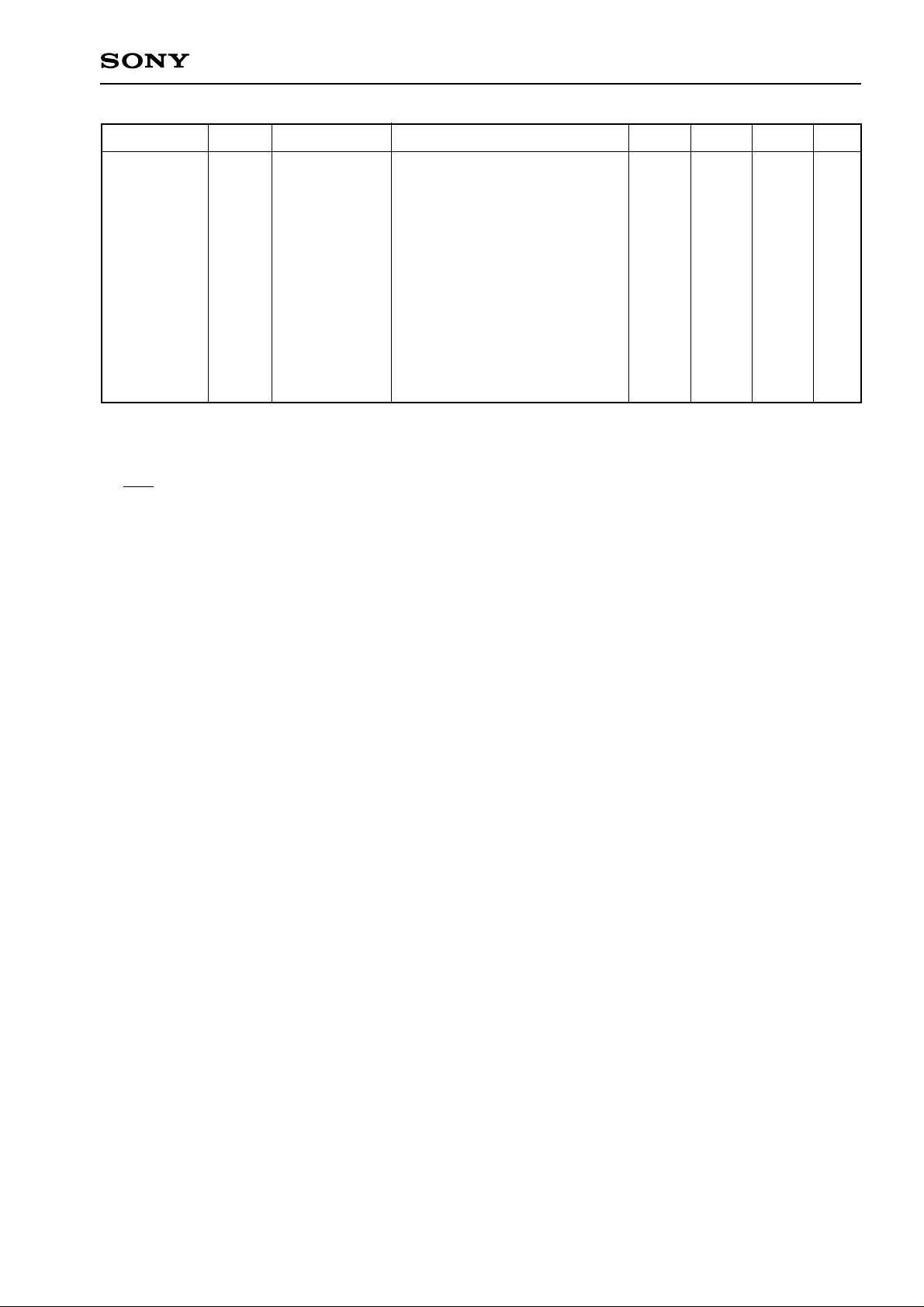
CXP83232A/83240A
Item Symbol Pins Conditions Min.
Typ. Max. Unit
Pins other than
PB7, PE5, PE6
VLC1 to VLC3
COM0 to COM3
SEG0 to SEG15
Clock 1MHz
0V for all pins excluding
measured pins
10 20
Input capacity
CIN
PD0/SEG16 to
PD7/SEG23
PF0/SEG24 to
PF7/SEG31
PG0/SEG32 to
PG7/SEG39
AVREF, AVSS,
VDD, VSS
∗1
Common pins of PD0/SEG16 to PD7/SEG23, PF0/SEG24 to PF7/SEG31, PG0/SEG32 to PG7/SEG39,
PD, PF and PG is the case when the common pin is selected as port; SEG16 to SEG39 is when the
common pin is selected as segment output.
∗2
RST specifies the input current when pull-up resitor has been selected; leakage current when no resistor
has been selected.
∗3
Pins PA to PC, and PH specifies the input current when pull-up resistor has been selected; leakage current
when no resistor has been selected. (PE0 to PE4 specifies the leakage current.)
∗4
When all output pins are left open.
pF
– 15 –
Page 16
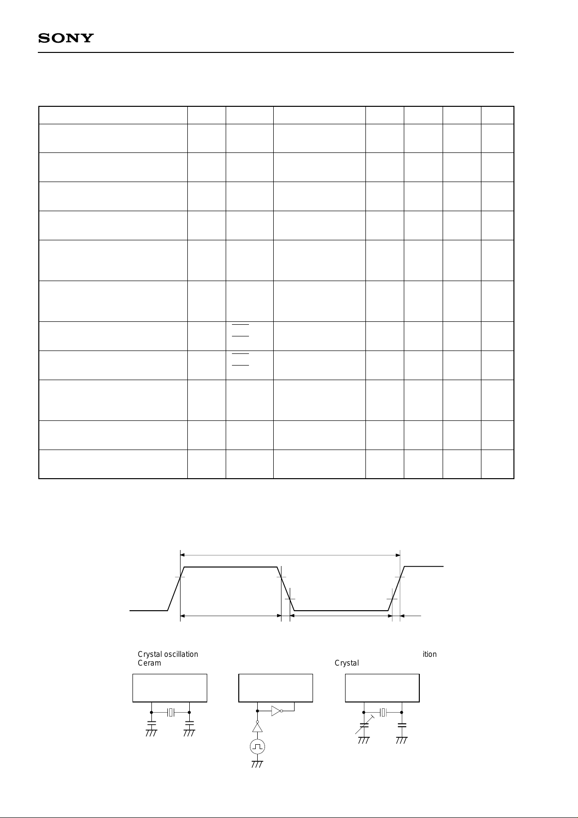
A
A
A
AC Characteristics
(1) Clock timing
CXP83232A/83240A
(Ta = –20 to +75°C, VDD = 4.5 to 5.5V, Vss = 0V)
Item Symbol Pin Conditions Min. Unit
System clock frequency
System clock input
pulse width
System clock input rise and
fall time
System clock frequency
System clock input pulse width
System clock input rise and
fall time
Event count input clock pulse
width
Event count input clock rise
and fall time
System clock frequency
fC
tXL,
tXH
tCR,
tCF
fC
tXL,
tXH
tCR,
tCF
tEH,
tEL
tER,
tEF
fC
XTAL1
EXTAL1
EXTAL1
EXTAL1
XTAL2
EXTAL2
EXTAL2
EXTAL2
EC0
EC1
EC0
EC1
TEX
TX
Fig. 1, Fig. 2
Fig. 1, Fig. 2
external clock drive
Fig. 1, Fig. 2
external clock drive
VDD = 3.0 to 5.5V
Fig. 1, Fig. 2
VDD = 3.0 to 5.5V
Fig. 1, Fig. 2
external clock drive
VDD = 3.0 to 5.5V
Fig. 1, Fig. 2
external clock drive
Fig. 3
Fig. 3
VDD = 2.7 to 5.5V
Fig. 2 (32kHz clock
applied condition)
1
37.5
0.3
450
tsys+ 50
∗
32.768
Typ.
0.5
Max.
10
200
0.7
200
20
MHz
ns
ns
MHz
ns
ns
ns
ms
kHz
Event count input clock input
pulse width
Event count input clock rise
and fall time
∗
tsys indicates the three values below according to the upper two bits (CPU clock selection) of the clock
control register (address: 00FEH).
tTL,
tTH
tTR,
tTF
TEX
TEX
Fig. 3
Fig. 3
10
20
tsys (ns) = 2000/fc (upper two bits = "00"), 4000/fc (upper two bits = "01"), 16000/fc (upper two bits = "11").
Fig. 1. Clock timing
EXTAL1
EXTAL2
Fig. 2. Clock applied conditions
Crystal oscillation
Ceramic oscillation
EXTAL
AA
XTAL
XH tXLtCF tCR
t
EXTAL
1/fc
External clock
XTAL
AA
DD – 0.4V
V
0.4V
32kHz clock applied condition
Crystal oscillation
TEX
AA
TX
µs
ms
1 C2
C
74HC04
– 16 –
1 C2
C
Page 17
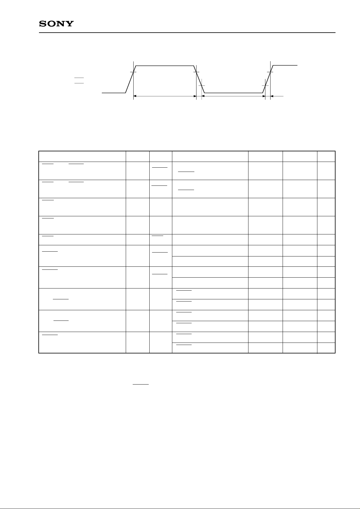
Fig. 3. Event count clock timing
CXP83232A/83240A
TEX
EC0
EC1
t
EH tELtEF tER
tTH tTLtTF tTR
(2) Serial transfer (CH0) (Ta = –20 to +75°C, VDD = 4.5 to 5.5V, Vss = 0V)
Item
CS0 ↓ → SCK0
delay time
CS0 ↑ → SCK0
float delay time
CS0 ↓ → SO0
delay time
CS0 ↑ → SO0
float delay time
CS0 high level width
SCK0 cycle time
Symbol Pin Min.
tDCSK
tDCSKF
tDCSO
tDCSOF
tWHCS
tKCY
SCK0
SCK0
SO0
SO0
CS0
SCK0
Chip select transfer mode
(SCK0 = output mode)
Chip select transfer mode
(SCK0 = output mode)
Chip select transfer mode
Chip select transfer mode
Chip select transfer mode
Input mode
Output mode
tsys + 200
2tsys + 200
16000/fc
0.8VDD
0.2VDD
tsys + 200
tsys + 200
tsys + 200
tsys + 200
Max.
UnitConditions
ns
ns
ns
ns
ns
ns
ns
SCK0 high and low level
widths
SI0 input setup time
(for SCK0 ↑)
SI0 input hold time
(for SCK0 ↑)
SCK0 ↓ → SO0
delay time
Note 1) tsys indicates the three values below according to the upper two bits (CPU clock selection) of the
clock control register (address: 00FEH).
tKH
tKL
tSIK
tKSI
tKSO
SCK0
SI0
SI0
SO0
Input mode
Output mode
SCK0 input mode
SCK0 output mode
SCK0 input mode
SCK0 output mode
SCK0 input mode
SCK0 output mode
tsys + 100
8000/fc – 50
100
200
tsys + 200
100
tsys + 200
100
ns
ns
ns
ns
ns
ns
ns
ns
tsys (ns) = 2000/fc (upper two bits = "00"), 4000/fc (upper two bits = "01", 16000/fc (upper two bits = "11")
Note 2) The load condition for the SCK0 output mode, SO0 output delay time is 50pF + 1TTL.
– 17 –
Page 18
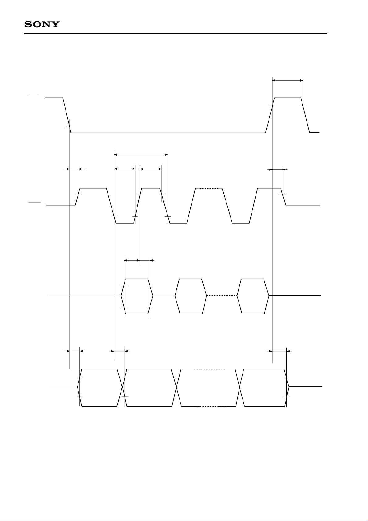
Fig. 4. Serial transfer CH0 timing
CXP83232A/83240A
tWHCS
CS0
SCK0
0.2V
DD
tKCY
tDCSK tDCSKF
tKL tKH
0.8VDD
0.2VDD
tKSI
t
SIK
0.8VDD
0.8VDD
SI0
SO0
t
DCSO
0.8VDD
Input data
0.2VDD
tKSO tDCSOF
Output data
0.8V
DD
0.2VDD
– 18 –
Page 19
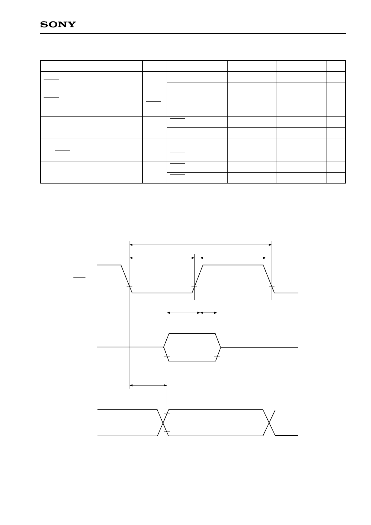
CXP83232A/83240A
Serial Transfer (CH1) (Ta = –20 to +75°C, VDD = 4.5 to 5.5V, Vss = 0V)
Item
SCK1 cycle time
SCK1 high and low level
widths
SI1 input setup time
(for SCK1 ↑)
SI1 input hold time
(for SCK1 ↑)
Symbol Pin Conditions Min. Max. Unit
tKCY
tKH
tKL
tSIK
tKSI
SCK1
Input mode
Output mode
input mode
SCK1
Output mode
SCK1 input mode
SI1
SCK1 output mode
SCK1 input mode
SI1
SCK1 output mode
1000
16000/fc
400
8000/fc – 50
100
200
200
100
SCK1 input mode
SCK1 ↓ → SO1 delay time
tKSO
SO1
SCK1 output mode
Note) The load condition for the SCK1 output mode, SO1 output delay time is 50pF + 1TTL.
Fig. 5. Serial transfer CH1 timing
tKCY
200
100
ns
ns
ns
ns
ns
ns
ns
ns
ns
ns
SCK1
SI1
SO1
tKL tKH
tSIK
Input data
tKSO
0.8VDD
0.2VDD
0.8VDD
0.2VDD
tKSI
0.8VDD
0.2VDD
Output data
– 19 –
Page 20
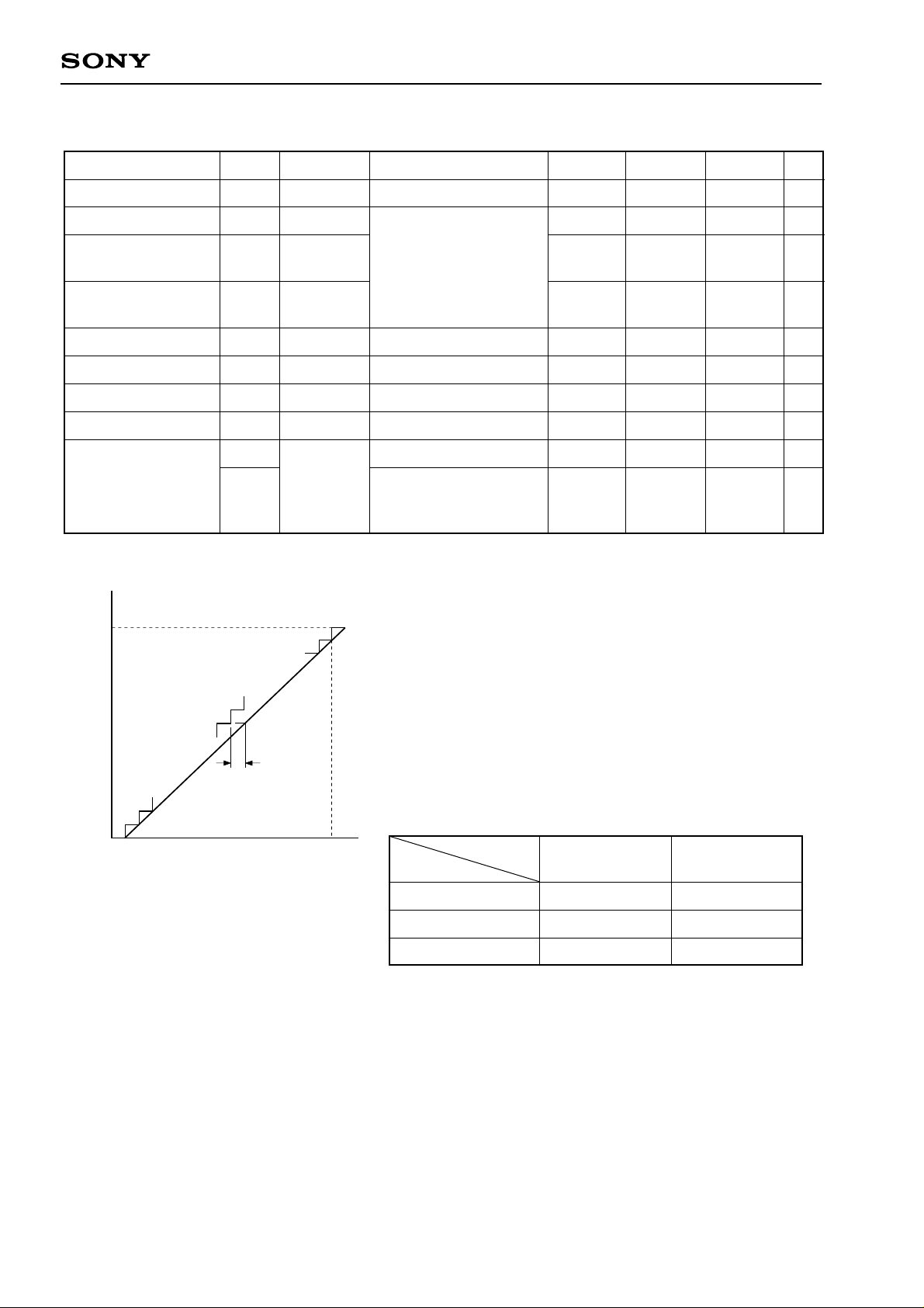
CXP83232A/83240A
(3) A/D converter characteristics (Ta = –20 to +75°C, VDD = 4.5 to 5.5V, Vss = AVSS = 0V)
Item Symbol Pin Conditions Min. Typ. Max. Unit
Resolution
Linearity error
Zero transition
voltage
Full-scale transition
voltage
Conversion time
Sampling time
Reference input voltage
Analog input voltage
∗1
VZT
∗2
VFT
tCONV
tSAMP
VREF
VIAN
AVREF
AN0 to AN7
IREF
AVREF current
AVREF
IREFS
Fig. 6. Definition of A/D converter terms
FFH
FEH
Ta = 25°C
VDD = AVREF = 5.0V
VSS = AVSS = 0V
Operation mode
SLEEP mode
STOP mode
32kHz operation mode
8
±3 LSB
–10
4910 mV
160/fADC
12/fADC
∗3
∗3
10
4970
VDD – 0.5
0
0.6
70 mV
5030
VDD
AVREF
1.0
10 µA
Bits
µs
µs
V
V
mA
Digital conversion value
01H
00H
Linearity error
Analog input
∗
1
VZT: Value at which the digital conversion value changes
from 00H to 01H and vice versa.
∗
2
VFT: Value at which the digital conversion value changes
from FEH to FFH and vice versa.
∗
3
fADC indicates the below values due to the Bit 6 (CKS) of
A/D control register (address: 00F9H) and the Bit 7 (PCK1)
and Bit 6 (PCK0) of clock control register (address: 00FFH).
V
FTVZT
CKS
0 (φ/2 selection)
1 (φ selection)
PCK1, PCK0
00 (φ = fEX/2)
01 (φ = fEX/4)
11 (φ = fEX/16)
fADC = fC/2
fADC = fC/4
fADC = fC/16
fADC = fC
fADC = fC/2
fADC = fC/8
– 20 –
Page 21
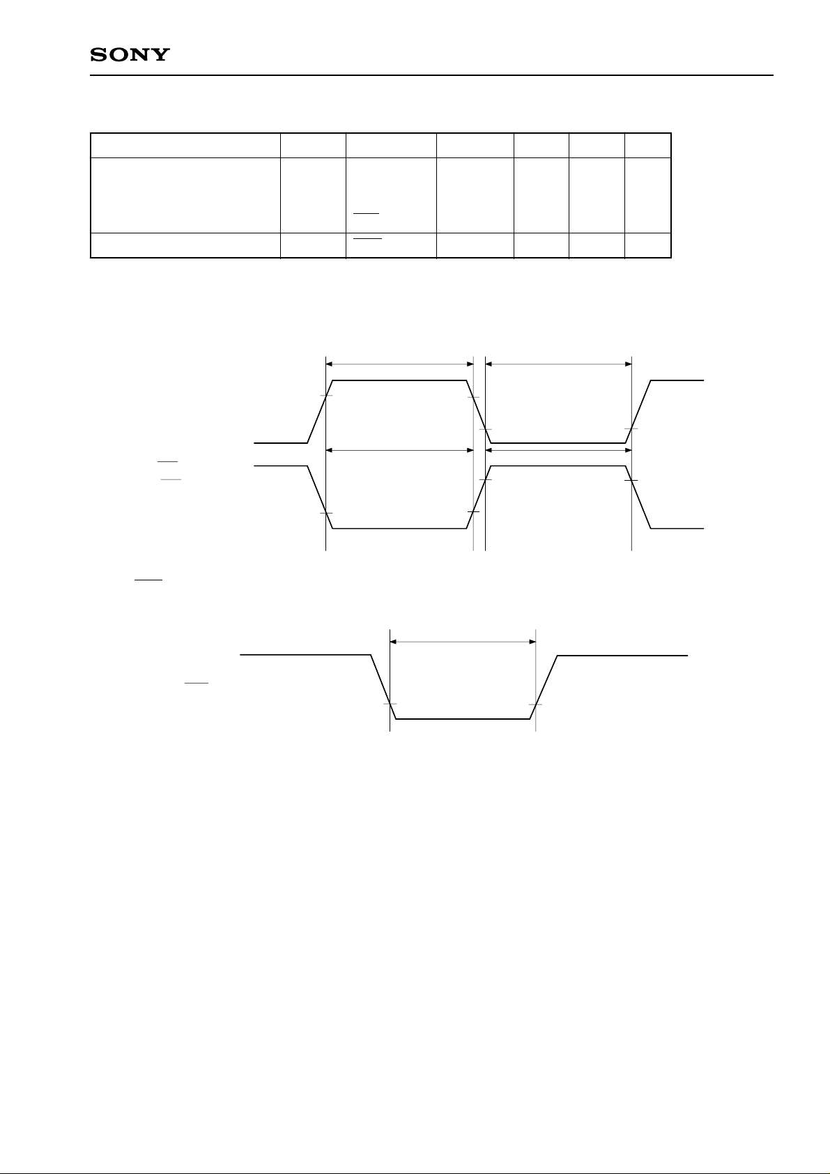
(4) Interruption, reset input (Ta = –20 to +75°C, VDD = 4.5 to 5.5V, Vss = 0V)
CXP83232A/83240A
Item
External interruption
high and low level widths
Reset input low level width
Fig. 7. Interruption input timing
INT0
INT1
INT2
NMI/INT3
(NMI specifies only
for the falling edge)
Symbol Pin
INT0
tIH
tIL
INT1
INT2
NMI/INT3
tRSL
RST
Conditions
Min. Max.
1
32/fc
tIH tIL
0.8VDD
tIL
Unit
µs
µs
0.2VDD
tIH
Fig. 8. RST input timing
RST
tRSL
0.2VDD
– 21 –
Page 22
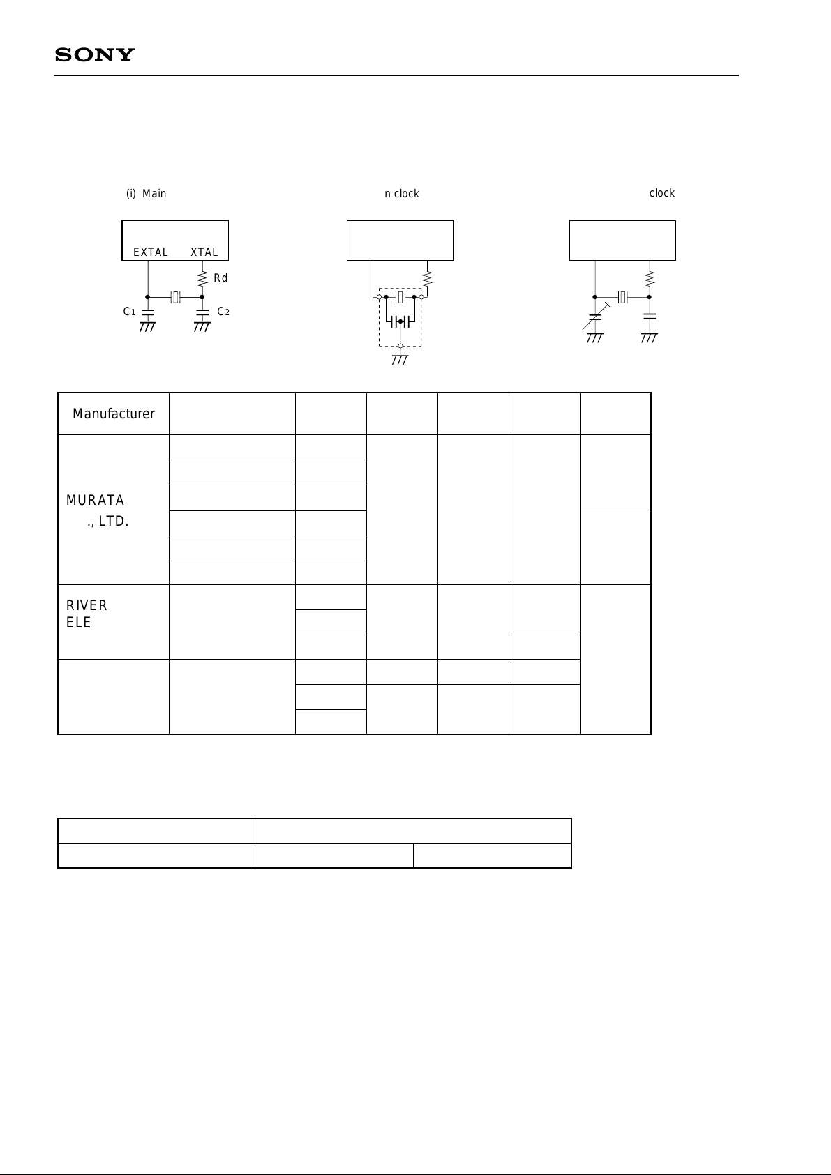
Appendix
A
A
A
A
A
Fig. 9. SPC700 series recommended oscillation circuit
CXP83232A/83240A
(i) Main clock
500kHz sub clock
EXTAL
AA
AA
C
1 C2
Manufacturer
MURATA MFG
CO., LTD.
RIVER
ELETEC
CO., LTD.
XTAL
Rd
Model
CSA4.19MG
CSA8.00MG
CSA10.0MT
CST4.19MGW
CST8.00MTW
CST10.00MTW
HC-49/U03
∗
∗
∗
fc (MHz)
4.19
8.00
10.00
4.19
8.00
10.00
4.19
8.00
10.00
4.19
(ii) Main clock
500kHz sub clock
EXTAL
XTAL
AA
Rd
C1 C2
C1 (pF) C2 (pF) Rd (Ω)
30
15
22
30
15
22 560
(iii) 32kHz sub clock
EXTAL
AAA
AAA
1 C2
C
0
2.2k
470
TEX
Circuit
example
(i)
(ii)
(i)
XTAL
TX
Rd
KINSEKI LTD.
Those marked with an asterisk (∗) signify types with built-in ground capacitance (C1, C2).
Mask Option Table
Reset pin pull-up resistor Non-existent
HC-49/U (-S)
Item
8.00
10.00
18 18
Content
0
Existent
– 22 –
Page 23

Characteristics Curves
CXP83232A/83240A
(Ta = 25°C, typical)
20.0
10.0
5.0
1.0
0.5
– Supply current [mA]
DD
I
0.1
(100µA)
0.05
(50µA)
0.01
(10µA)
2
VDD – Supply voltage [ V ]
IDD vs. VDD
4
3
fc = 10MHz main clock
1/2 frequency dividing mode
fc = 500kHz sub clock
1/2 frequency dividing mode
fc = 10MHz main clock
SLEEP mode
fc = 500kHz sub clock
SLEEP mode
32kHz mode
(Instruction)
32kHz
SLEEP mode
5
7
6
(VDD = 5V, Ta = 25°C, typical)
20
15
10
– Supply current [mA]
DD
I
5
0
510
fc – System clock [MHz]
IDD vs. fc
Main clock
1/2 frequency
dividing mode
Main clock
SLEEP mode
15
– 23 –
Page 24

CXP83232A/83240A
Package Outline Unit: mm
SONY CODE
EIAJ CODE
JEDEC CODE
0.65
0° to 15°
100PIN QFP (PLASTIC)
23.9 ± 0.4
+ 0.4
20.0 – 0.1
±0.12
M
0.15
(16.3)
DETAIL A
QFP-100P-L01
∗QFP100-P-1420-A
0.8 ± 0.2
+ 0.1
0.15 – 0.05
+ 0.4
15.8 ± 0.4
17.9 ± 0.4
14.0 – 0.01
PACKAGE STRUCTURE
PACKAGE MATERIAL
LEAD TREATMENT
LEAD MATERIAL
PACKAGE WEIGHT
EPOXY RESIN
SOLDER PLATING
COPPER / 42 ALLOY
1.4g
A
+ 0.35
2.75 – 0.15
76
100
0.5 ± 0.08
SONY CODE
EIAJ CODE
JEDEC CODE
100PIN LQFP (PLASTIC)
16.0 ± 0.2
∗ 14.0 ± 0.1
75
1
+ 0.08
0.18 – 0.03
0.1 ± 0.1
0° to 10°
DETAIL A
LQFP-100P-L01
∗QFP100-P-1414-A
0.5 ± 0.2
51
50
(15.0)
A
26
(0.22)
25
+ 0.2
1.5 – 0.1
0.127 – 0.02
0.5 ± 0.2
+ 0.05
0.1
NOTE: Dimension “∗” does not include mold protrusion.
PACKAGE STRUCTURE
PACKAGE MATERIAL
LEAD TREATMENT
LEAD MATERIAL
PACKAGE WEIGHT
EPOXY/PHENOL RESIN
SOLDER PLATING
42 ALLOY
– 24 –
 Loading...