

Page 1
CXP82532/82540
CMOS 8-bit Single Chip Microcomputer
Description
The CXP82532/82540 microcomputer is composed
of a CPU, ROM RAM, and I/O ports. These chips
feature many other high-performance circuits in a
single-chip CMOS design, including an A/D
converter, serial interface, timer/counter, time-base
timer, capture timer/counter, fluorescent display
controller/driver, remote control receiver.
This device also includes a power-on reset function
and sleep/stop functions which can be used to
achieve low power consumption.
Features
• Instruction set which supports a wide array of data types
— 213 types of instructions which include 16-bit calculations, multiplication and division arithmetic, and
boolean bit operations.
• Minimum instruction cycle 400ns for 10MHz operation
• On-chip ROM 32K bytes (CXP82532)
40K bytes (CXP82540)
• On-chip RAM 1120 bytes (Including fluorescent display data area)
• Peripheral functions:
— A/D converter 8-bit, 8-channel, successive approximation system
(conversion time 32µs/10MHz)
— Serial interface On-chip 8-bit, 8-stage FIFO (1 to 8 bytes auto transfer) 1 channel
8-bit clock synchronized 1 channel
— Timers 8-bit timer
8-bit timer/counter
19-bit time-base timer
16-bit capture timer/counter
— Fluorescent display controller/driver
Maximum of 336 segment display available
1 to 16 digits dynamic display
Dimmer function
High voltage tolerance output (40V)
On-chip pull-down resistor (Mask option)
— Remote control receiver circuit
On-chip noise elimination circuit
On-chip 6 stage FIFO 8-bit pulse measurement counter
• Interrupts 14 factors, 15 vectors multi-interruption possible
• Standby mode Sleep/stop
• Package 80-pin plastic QFP
• Piggyback/evaluator CXP82500 80-pin ceramic QFP
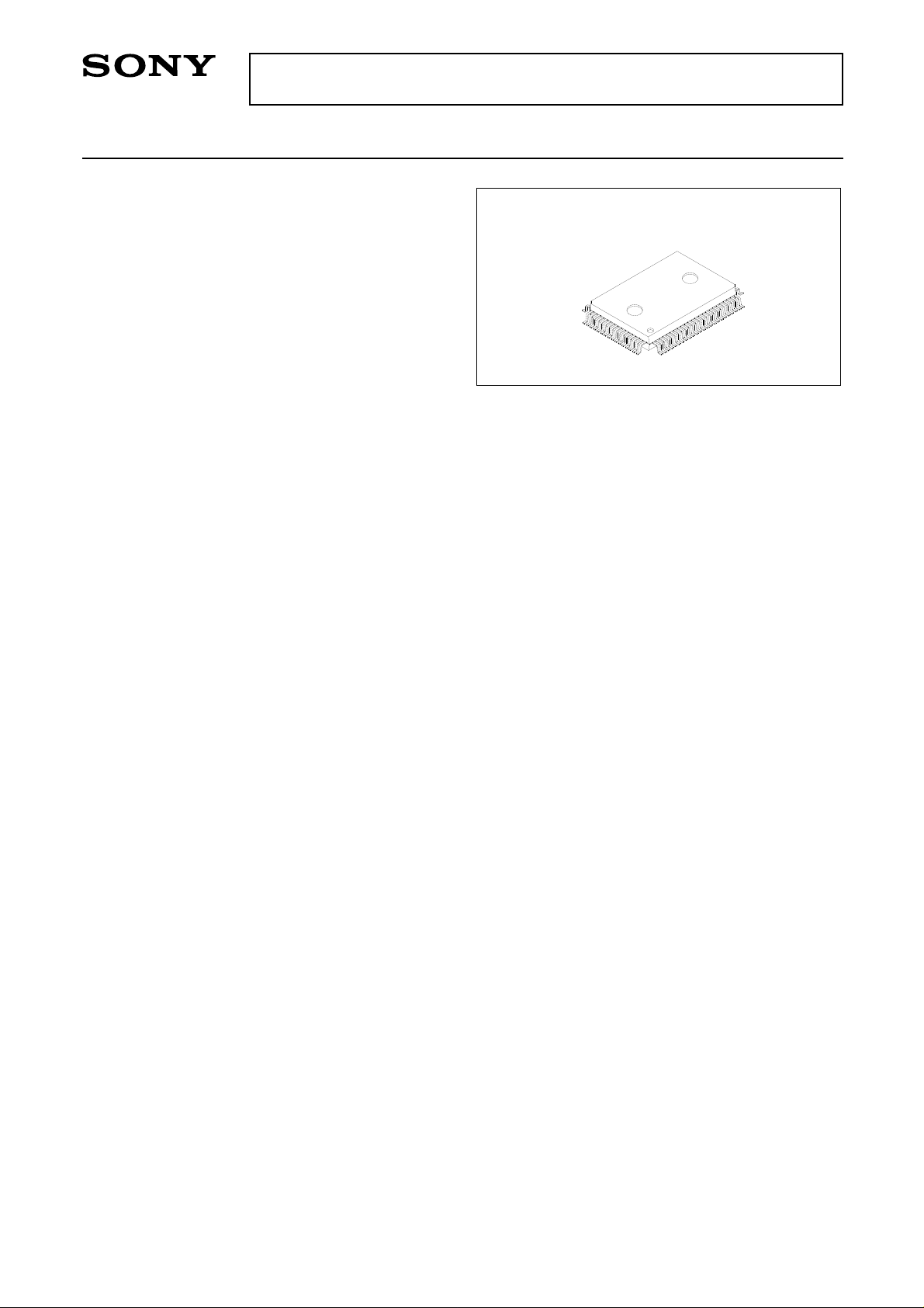
80 pin QFP (Plastic)
Structure
Silicon gate CMOS IC
Sony reserves the right to change products and specifications without prior notice. This information does not convey any license by
any implication or otherwise under any patents or other right. Application circuits shown, if any, are typical examples illustrating the
operation of the devices. Sony cannot assume responsibility for any problems arising out of the use of these circuits.
– 1 –
E92Y32A78-PS
Page 2
CXP82532/82540
SS
V
V
DD
RST
XTAL
EXTAL
PA0 to PA7
8
PB0 to PB6
PB7
7
PORT A
CLOCK GEN./
SYSTEM CONTROL
SPC700
CPU CORE
PORT B
PC0 to PC7
8
PORT C
RAM
1040 BYTES
ROM
32/40K BYTES
PD0 to PD7
8
PE0 to PE5
6
PORT D
PE6 to PE7
2
PF0 to PF7
8
PORT E
PORT F
PRESCALER/
PG0 to PG3
4
PORT G
TIME BASE TIMER
INT3
INT2
INT1
INT0
RAM
80 BYTES
A/D CONVERTER
FDP
CONTROLLER/
8
8
8
T8/S28
T15/S21
T0 to T7
AN0 to AN7
DRIVER
21
FDP
V
S0 to S20
FIFO
REMOCON
RMC
INTERRUPT CONTROLLER
2
FIFO
UNIT 0
SERIAL
INTERFACE
SI0
CS0
SO0
SCK0
SERIAL INTERFACE UNIT 1
SI1
SO1
8 BIT TIMER/COUNTER 0
EC0
SCK1
2
8 BIT TIMER 1
16 BIT CAPTURE
TIMER/COUNTER 2
TO
EC1
CINT
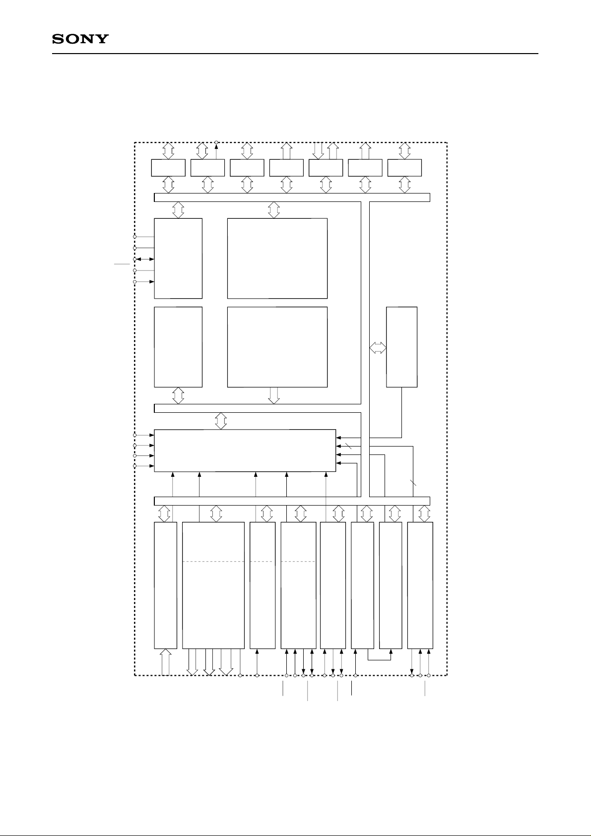
Block Diagram
– 2 –
Page 3

Pin Assignment (Top View)
PE1/EC1/INT1
PE2/IN2
PE0/EC0/INT0
PG3
PG2
PG1
PG0
NC
DD
V
FDP
V
T0
T1
T2
T3
T4
CXP82532/82540
T5
PE3/INT3
PE4/RMC
PE5
PE6
PE7/TO
PB0/CINT
PB1/CS0
PB2/SCK0
PB3/SI0
PB4/SO0
PB5/SCK1
PB6/SI1
PB7/SO1
PC0/KR0
PC1/KR1
PC2/KR2
PC3/KR3
PC4/KR4
PC5/KR5
PC6/KR6
PC7/KR7
PA0/AN0
PA1/AN1
PA2/AN2
10
11
12
13
14
15
16
17
18
19
20
21
22
23
24
80
78
79
1
2
3
4
5
6
7
8
9
77
76
75
74
73
72
71
70
69
68
67
66
65
64
63
62
61
60
59
58
57
56
55
54
53
52
51
50
49
48
47
46
45
44
43
42
41
T6
T7
T8/S28
T9/S27
T10/S26
T11/S25
T12/S24
T13/S23
T14/S22
T15/S21
S20
S19
S18
S17
S16
PF7/S15
PF6/S14
PF5/S13
PF4/S12
PF3/S11
PF2/S10
PF1/S9
PF0/S8
PD7/S7
25
26
PA3/AN3
27
28
PA4/AN4
PA5/AN5
29
PA7/AN7
PA6/AN6
30
31
RST
32
XTAL
EXTAL
33
SS
V
34
Note) NC (Pin 73) is always connected to VDD.
– 3 –
35
PD1/S1
PD0/S0
36
PD2/S2
37
PD3/S3
38
PD4/S4
39
PD5/S5
40
PD6/S6
Page 4
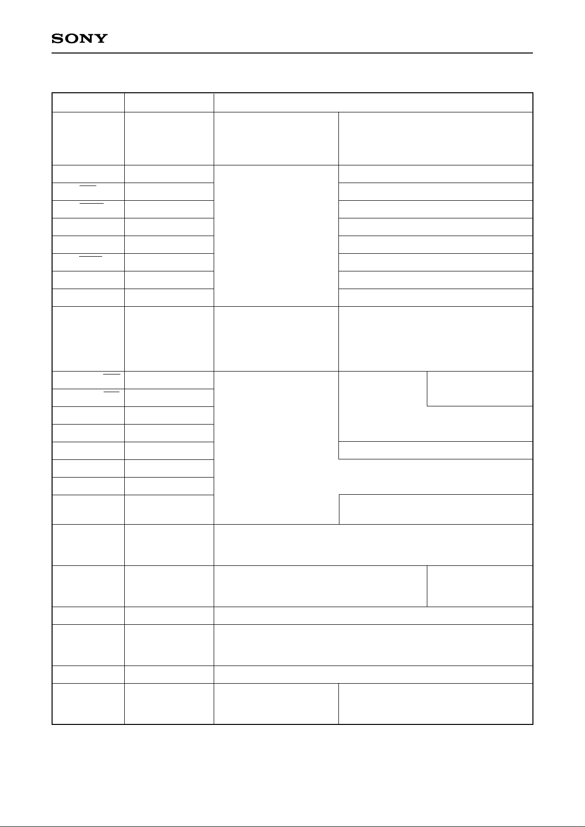
Pin Description
Symbol I/O Description
CXP82532/82540
PA0/AN0
to
PA7/AN7
PB0/CINT
PB1/CS0
PB2/SCK0
PB3/SI0
PB4/SO0
PB5/SCK1
PB6/SI1
PB7/SO1
PC0/KR0
to
PC7/KR7
PE0/INT0/EC0
PE1/INT1/EC1
PE2/INT2
PE3/INT3
PE4/RMC
PE5
PE6
I/O/Analog input
I/O/Input
I/O/Input
I/O/I/O
I/O/Input
I/O/Output
I/O/I/O
I/O/Input
Output/Output
I/O/Input
Input/Input/Input
Input/Input/Input
Input/Input
Input/Input
Input/Input
Input
Output
(Port A)
8-bit port; single bit
addressable.
(8 pins)
(Port B)
Single bit addressable from
amongst lower 7 bits;
highest bit (PB7)
dedicated to output.
(8 pins)
(Port C)
8-bit port; single bit
addressable. Can provide
12mA sink current.
(8 pins)
(Port E)
8-bit port with lower 6 bits
dedicated to input and
upper 2 bits dedicated to
output.
(8 pins)
Analog input to A/D converter.
(8 pins)
External capture input for 16-bit timer/counter.
Chip select input for serial interface (CH0).
Serial clock (CH0) input/output.
Serial data (CH0) input.
Serial data (CH0) output.
Serial clock (CH1) input/output.
Serial data (CH1) input.
Serial data (CH1) output.
Key return input for FDP segment signal
which performs key scanning.
External event input
to timer/counter.
Input for external
(2 pins)
interrupt requests.
(4 pins)
Input for remote control receiver circuit.
PE7/TO
PG0 to PG3
PF0/S8
to
PF7/S15
S16 to S20
T8/S28
to
T15/S21
T0 to T7
PD0/S0
to
PD7/S7
Output/Output
I/O
Output/Output
Output
Output/Output
Output
Output/Output
Output pin for 16-bit timer/counter
rectangular waveform.
(Port G)
4-bit input/output port; single bit addressable.
(4 pins)
(Port F)
8-bit dedicated output port.
(8 pins)
Segment signal
output for FDP.
Segment signal output for FDP.
Dual purpose output for FDP timing and segment signals.
Timing signal output for FDP.
(Port D)
8-bit dedicated output port.
Segment signal output for FDP.
(8 pins)
– 4 –
Page 5
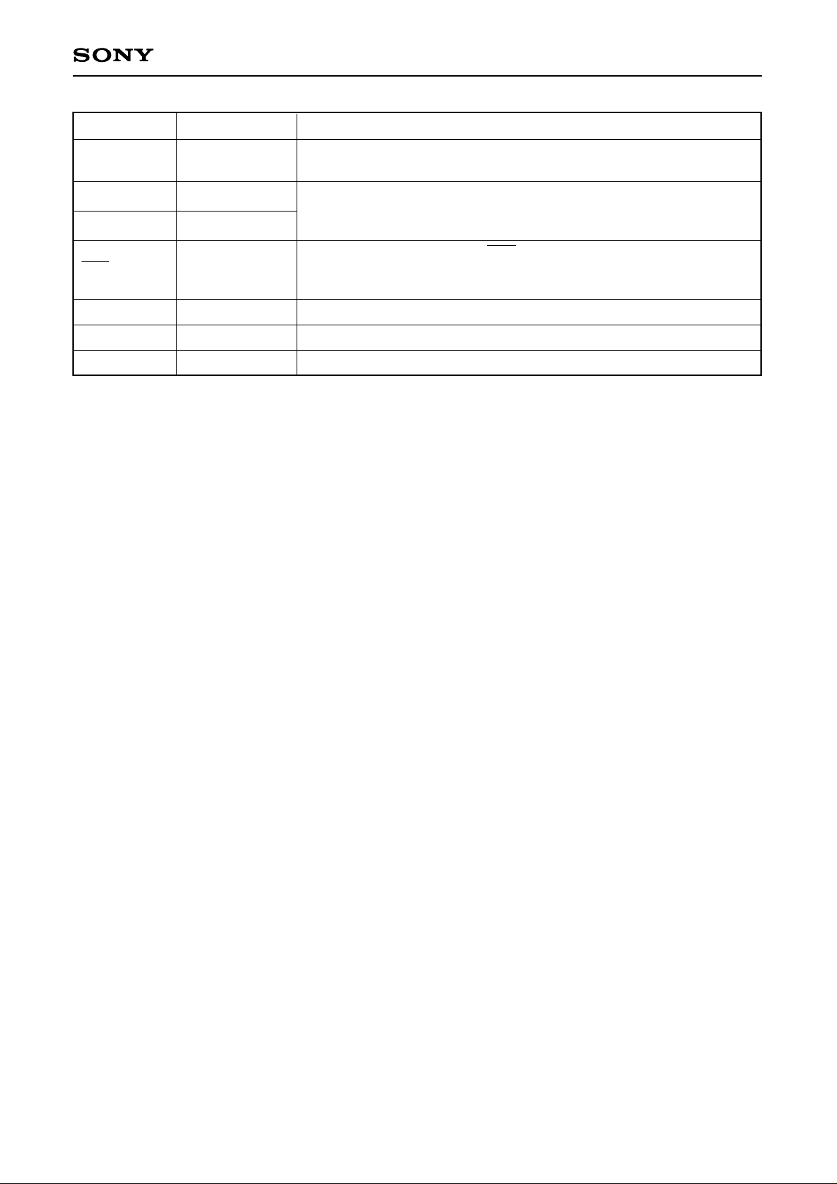
Symbol I/O Description
CXP82532/82540
VFDP
EXTAL
XTAL
RST
NC
VDD
VSS
Input
Output
I/O
Provides voltage for FDP when on-chip resistor is selected under mask
option.
Connection for system clock oscillation crystal. When using an external
clock, input normal signal to EXTAL and reverse phase signal to the
XTAL pin.
System reset, active "L". The RST pin is an input/output pin which
outputs a "L" level from the on-chip power-on reset circuit when the
power is turned on. (Mask option)
NC pin is always connected to VDD.
Positive power supply pin.
GND
– 5 –
Page 6
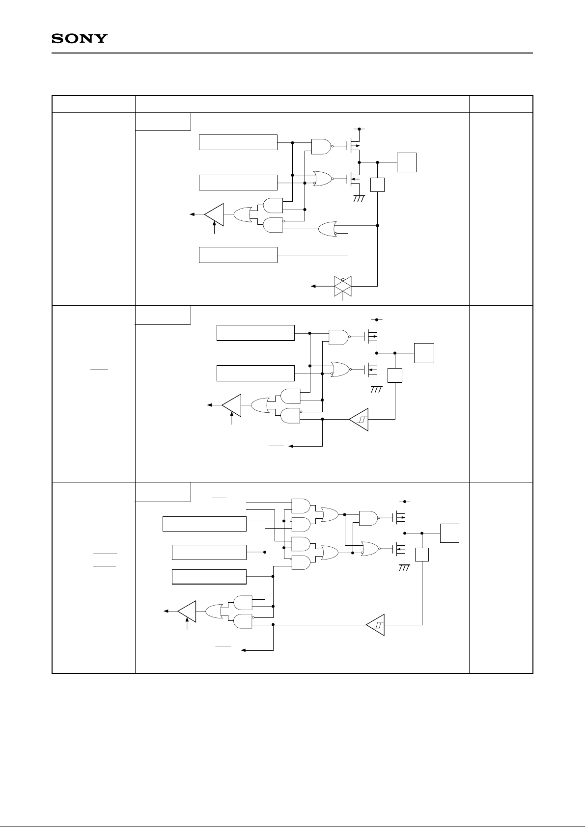
Input/Output Circuit Formats for Pins
CXP82532/82540
Pin
PA0/AN0
to
PA7/AN7
8 pins
PB0/CINT
PB1/CS0
PB3/SI0
PB6/SI1
Port A
Data bus
Port B
Data bus
Port A data
Port A direction
"0" when reset
RD (Port A)
Port A input select
"0" when reset
Port B data
Port B direction
"0" when reset
Circuit format
A/D converter
Input multiplexer
Schmitt input
IP
When reset
Input
protection
circuit
Hi-Z
IP
Hi-Z
4 pins
PB2/SCK0
PB5/SCK1
2 pins
Port B
Port B output select
"0" when reset
"0" when reset
Data bus
SCK OUT
Output enable
Port B data
Port B direction
RD (Port B)
SCK in
RD (Port B)
CINT
CS0
SI0
SI1
IP
Hi-Z
Schmitt input
– 6 –
Page 7
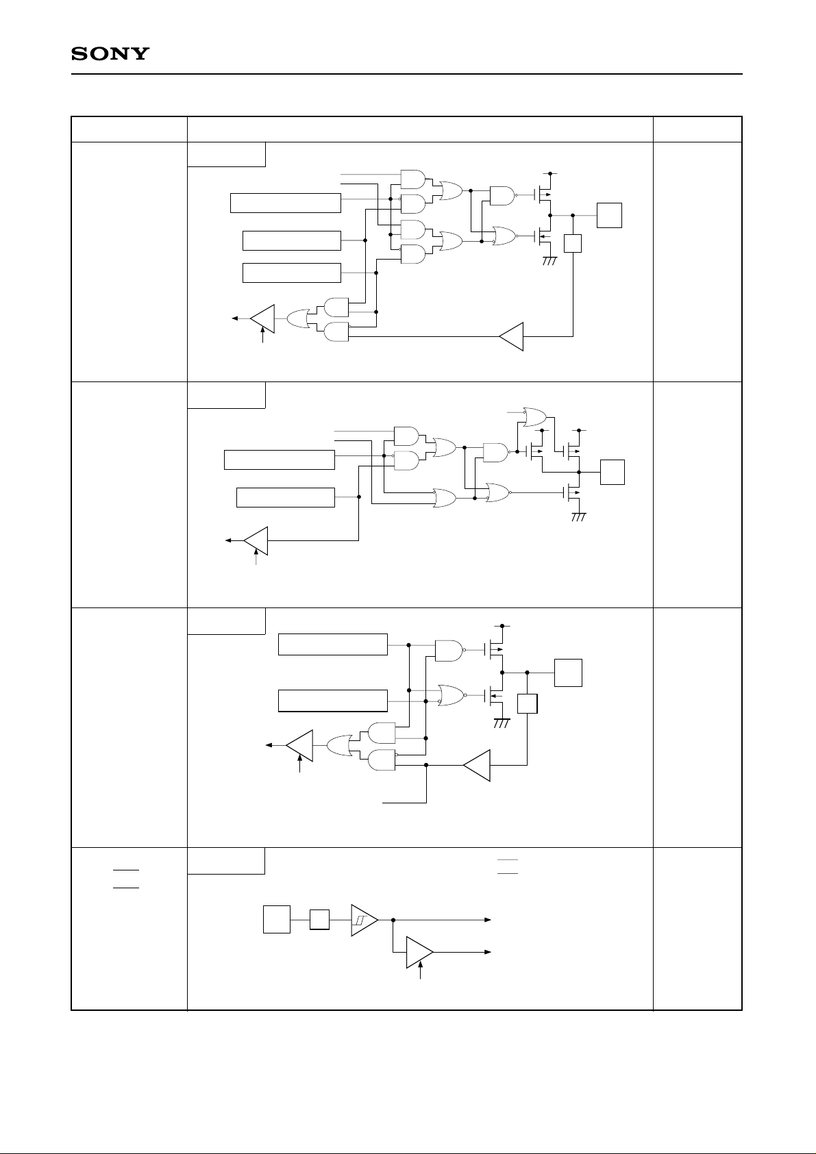
CXP82532/82540
PB4/SO0
1 pin
PB7/SO1
1 pin
Port B
Port B output select
"0" when reset
"0" when reset
Data bus
Port B
Port B output select
"0" when reset
"1" when reset
Data bus
RD (Port B)
Output enable
Port B data
Port B direction
RD (Port B)
Output enable
Port B data
SO
SO
Circuit format
Internal reset signal
∗
Pull-up transistor
about 200kΩ
When resetPin
IP
Hi-Z
∗
High level
PC0/KR0
to
PC7/KR7
8 pins
PE0/EC0/INT0
PE1/EC1/INT1
PE2/INT2
PE3/INT3
PE4/RMC
5 pins
Port C
Data bus
Port E
Port C data
Port C direction
"0" when reset
RD (Port C)
Key input signal
Schmitt input
IP
∗
IP
∗
Capable of driving 12mA large current
EC0/INT0
EC1/INT1
INT2
INT3
RMC
Data bus
RD (Port E)
Hi-Z
Hi-Z
– 7 –
Page 8

CXP82532/82540
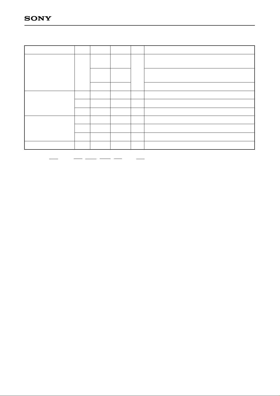
Pin
PE5
1 pin
PE6
1 pin
PE7/TO
Port E
Port E
"1" when reset
Port E
Port E output select
"0" when reset
"1" when reset
Data bus
IP
Port E data
TO
Output enable (T2OE)
Port E data
Circuit format
RD (Port E)
Data bus
When reset
Hi-Z
High level
High level
1 pin
PG0
to
PG3
4 pins
Port G
RD (Port E)
"0" when reset
Data bus
Port G data
Port G direction
RD (Port G)
IP
Hi-Z
– 8 –
Page 9

CXP82532/82540
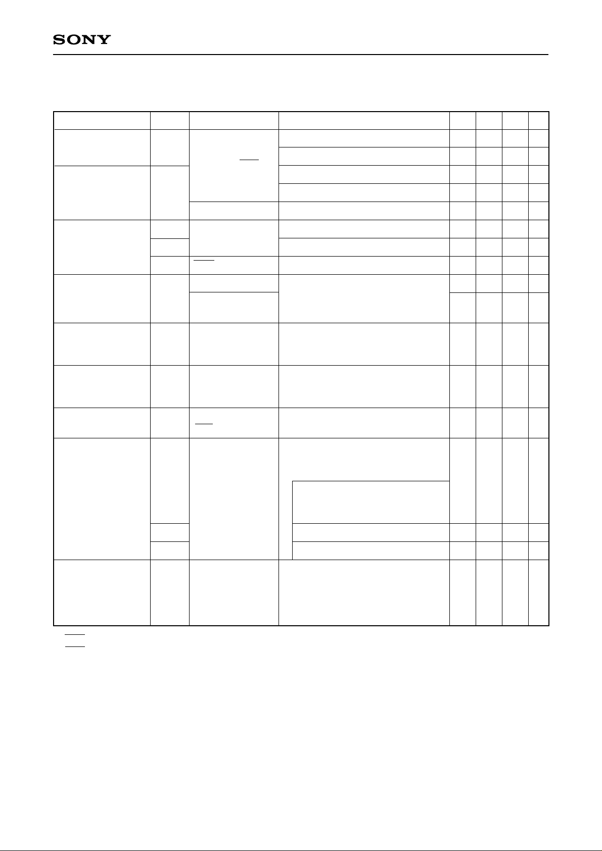
Pin
PD0/S0
to
PD7/S7
PF0/S8
to
PF7/S15
16 pins
S16 to S20
T15/S21
to
T8/S28
T0 to T7
21 pins
Port D
Port F
Segment output data
Output selection control signal
("0" when reset)
Port D data or
Port F data
"0" when reset
Data bus
RD (Port D or Port F)
Segment output data
Output selection control signal
("0" when reset)
Circuit format
∗
High voltage tolerance transistor
∗
Mask option
OP
Pull-down
resistor
VFDP
∗
High voltage tolerance transistor
∗
Mask option
OP
Pull-down
resistor
VFDP
When reset
Hi-Z or
Low level
(when PD
resistor is
connected)
Hi-Z or
Low level
(when PD
resistor is
connected)
EXTAL
XTAL
2 pins
RST
1 pin
EXTAL
XTAL
Pull-up resistor
Mask option
OP
IPIP
IP
From power-on reset circuit
(Mask option)
∗
Diagram shows
circuit construction
for oscillation.
∗
During stop
feedback resistor is
disconnected.
Schmitt input
Oscillation
Low level
– 9 –
Page 10

CXP82532/82540
Absolute Maximum Ratings (Vss = 0V)
Item Symbol Rating Unit Remarks
Supply voltage
Input voltage
Output voltage
Display output voltage
High level output current
High level total output current
Low level output current
Low level total output current
Operating temperature
Storage temperature
Allowable power dissipation
VDD
VIN
VOUT
VOD
IOH
IODH1
IODH2
∑IOH
∑IODH
IOL
IOLC
∑IOL
Topr
Tstg
PD
–0.3 to +7.0
–0.3 to +7.0
–0.3 to +7.0
VDD – 40 to
VDD + 0.3
–5
–15
–35
–40
–100
15
20
100
–20 to +75
–55 to +150
600
∗1
∗1
V
V
V
As P channel transistor is open drain,
V
VDD voltage is determined as standerd.
Other than display output pins
mA
Display outputs S0 to S20: per pin
mA
Display outputs T0 to T7,
mA
T8/S28 to T15/S21: per pin
Total of other than display output pins
mA
Total of display output pins
mA
Port 1 pin
mA
Large current port pin
mA
Entire pin total
mA
∗3
°C
°C
mW
∗2
: per pin
∗1
VIN and VOUT cannot exceed VDD + 0.3V.
∗2
Rating for output current of general input/output port.
∗3
The large current drive transistor is an N-channel transistor of Port C.
Note) If the absolute maximum ratings are exceeded, the LSI could reach permanent breakdown. Also,
observing recommended operating conditions is desirable; otherwise, the LSI's reliability could be
affected.
– 10 –
Page 11
CXP82532/82540
Recommended Operating Conditions (Vss = 0V)
Item Symbol Min. Max. Unit Remarks
4.5
Supply voltage
VDD
3.5
2.5
VIH
High level input
voltage
VIHS
VIHEX
VIL
Low level input
voltage
VILS
VILEX
Operating temperature
∗1
All regular input ports (PA, PB3, PB4, PB6, PC, PE5, PG).
∗2
For pins RST, CINT, CS0, SCK0, SCK1, EC0/INT0, EC1/INT1 , INT2, INT3, RMC.
∗3
Rating only for external clock input.
Topr
0.7VDD
0.8VDD
VDD – 0.4
0
0
–0.3
–20
5.5
5.5
5.5
VDD
VDD
VDD + 0.3
0.3VDD
0.2VDD
0.4
+75
High-speed mode (1/2, 1/4 clock) guaranteed
range during operation
V
Low-speed mode (1/16 clock) guaranteed range
during operation
Guaranteed data hold range during stop
∗1
V
Hysteresis input
V
EXTAL pin
V
∗1
V
Hysteresis input
V
EXTAL pin
V
∗3
∗3
°C
∗2
– 11 –
Page 12
CXP82532/82540
Electrical Characteristics
DC Characteristics (Ta = –20 to +75°C, Vss = 0V)
Item Symbol Pins Conditions Min.
High level
output voltage
Low level
output voltage
Input current
Display output
current
Open drain output
leak current
(P-CH Tr off state)
Pull-down
resistor
∗3
VOH
VOL
IIHE
IILE
IILR
IOH
ILOL
RL
PA, PB, PC,PE6,
PE7, PG, RST
∗1
(for VOL only)
PC
EXTAL
∗2
RST
S0 to S20
S21/T15 to S28/T8
T0 to T7
S0 to S20
S21/T15 to S28/T8
T0 to T7
S0 to S20
S21/T15 to S28/T8
T0 to T7
VDD = 4.5V, IOH = –0.5mA
VDD = 4.5V, IOH = –1.2mA
VDD = 4.5V, IOL = 1.8mA
VDD = 4.5V, IOL = 3.6mA
VDD = 4.5V, IOL = 12.0mA
VDD = 5.5V, VIH = 5.5V
VDD = 5.5V, VIL = 0.4V
VDD = 5.5V, VIL = 0.4V
VDD = 4.5V
VOH = VDD – 2.5V
VDD = 5.5V
VOL = VDD – 35V
VFDP = VDD – 35V
VDD = 5V
VOD – VFDP = 30V
4.0
3.5
0.5
–0.5
–1.5
–8
–20
60
Typ.
100
Max. Unit
V
V
0.4
V
0.6
V
1.5
V
40
µA
–40
µA
–400
µA
mA
mA
–20
µA
270
kΩ
Input/output leak
current
IIZ
PA to PC, PE, PG,
∗2
RST
VDD = 5.5V
VI = 0, 5.5V
±10
VDD = 5.5V
High-speed mode
(1/2 clock) operation
Supply current
∗4
IDD1
VDD
10MHz crystal
oscillator
25
(C1 = C2 = 15pF)
IDDSL
IDDST
Sleep mode
Stop mode
3
For pins other
Input capacitance
CIN
than S0 to S28,
T0 to T7, PB7,
PE6, PE7, VDD,
1MHz clock
0V other than measured
10
VSS, VFDP
∗1
RST pin is rated only when the power-on circuit is selected under the mask option.
∗2
RST pin is rated for input current when the pull-up resistor is selected; otherwise it is rated for leak current.
∗3
Applies when the on-chip pull-down resistor is selected under the mask option.
∗4
All output pins are left open.
40
8
10
20
µA
mA
mA
µA
pF
– 12 –
Page 13
A
A
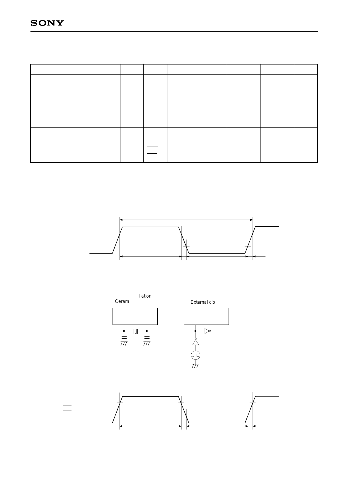
AC Characteristics
(1) Clock timing
CXP82532/82540
(Ta = –20 to +75°C, VDD = 4.5 to 5.5V, Vss = 0V)
Item Symbol Pins Conditions Unit
System clock frequency
System clock input pulse width
System clock input rising and
falling times
Event count input clock pulse
width
Event count input clock rising
and falling times
∗1
tsys is determind by the upper two bits of the clock control resister (Address: 00FEH; CPU clock selected)
resulting in one of the 3 following values:
fC
tXL,
tXH
tCR,
tCF
tEH,
tEL
tER,
tEF
XTAL
EXTAL
EXTAL
EXTAL
EC0,
EC1
EC0,
EC1
Fig. 1, Fig. 2
Fig. 1, Fig. 2
External clock driver
Fig. 1, Fig. 2
External clock driver
Fig. 3
Fig. 3
Min.
1
45
tsys + 50
Max.
10
200
∗1
20
tsys [ns] = 2000/fc (Upper 2 bits = "00"), 4000/fc (Upper 2 bits = "01"), 16000/fc (Upper 2 bits = "11")
Fig. 1. Clock timing
EXTAL
1/fc
DD – 0.4V
V
0.4V
MHz
ns
ns
ns
ms
Fig. 2. Clock applying condition
Crystal oscillation
Ceramic oscillation
C
Fig. 3. Event count clock timing
EC0
EC1
t
XH tXLtCF tCR
EXTAL
AA
1 C2
XTAL
tEH tELtEF tER
tTH tTLtTF tTR
External clock
EXTAL
AA
74HC04
XTAL
0.8VDD
0.2VDD
– 13 –
Page 14

CXP82532/82540
(2) Serial transfer (CH0) (Ta = –20 to +75°C, VDD = 4.5 to 5.5V, Vss = 0V)
Item
CS0 ↓ → SCK0
delay time
CS0 ↑ → SCK0
float delay time
CS0 ↓ → SO0
delay time
CS0 ↑ → SO0
float delay time
CS0 high level width
SCK0 cycle time
SCK0
high and low level width
SI0 input setup time
(against SCK0 ↑)
SI0 input hold time
(against SCK0 ↑)
SCK0 ↓ → SO0
delay time
Symbol Pin Min.
tDCSK
tDCSKF
tDCSO
tDCSOF
tWHCS
tKCY
tKH
tKL
tSIK
tKSI
tKSO
SCK0
SCK0
SO0
SO0
CS0
SCK0
SCK0
SI0
SI0
SO0
Chip select transfer mode
(SCK0 = output mode)
Chip select transfer mode
(SCK0 = output mode)
Chip select transfer mode
Chip select transfer mode
Chip select transfer mode
Input mode
Output mode
Input mode
Output mode
SCK0 input mode
SCK0 output mode
SCK0 input mode
SCK0 output mode
SCK0 input mode
SCK0 output mode
tsys + 200
2tsys + 200
16000/fc
tsys + 100
8000/fc – 50
100
200
tsys + 200
100
Max. UnitCondition
tsys + 200
tsys + 200
tsys + 200
tsys + 200
tsys + 200
100
ns
ns
ns
ns
ns
ns
ns
ns
ns
ns
ns
ns
ns
ns
ns
Note 1) tsys is determind by the upper two bits of the clock control resister (Address: 00FEH; CPU clock
selected) resulting in one of the 3 following values:
tsys [ns] = 2000/fc (Upper 2 bits = "00"), 4000/fc (Upper 2 bits = "01"), 16000/fc (Upper 2 bits = "11")
Note 2) The load of SCK0 output mode and SO0 output delay time is 50pF + 1TTL.
– 14 –
Page 15

Fig. 4. Serial transfer CH0 timing
CS0
0.2V
DD
CXP82532/82540
tWHCS
0.8VDD
tKCY
SCK0
SI0
tDCSK tDCSKF
tKL tKH
0.8VDD
0.2VDD
tSIK
tKSI
0.8VDD
Input
data
0.2VDD
0.8VDD
SO0
DCSO tKSO tDCSOF
t
Output data
– 15 –
0.8V
DD
0.2VDD
Page 16

CXP82532/82540
Serial transfer (CH1) (Ta = –20 to +75°C, VDD = 4.5 to 5.5V, Vss = 0V)
Item Symbol Pin Min. Max.Condition
SCK1 cycle time
SCK1 high and low
level width
SI1 input setup time
(against SCK1 ↑)
SI1 input hold time
(against SCK1 ↑)
tKCY
tKH
tKL
tSIK
tKSI
SCK1
Input mode
Output mode
Input mode
SCK1
Output mode
SCK1 input mode
SI1
SCK1 output mode
SCK1 input mode
SI1
SCK1 output mode
1000
16000/fc
400
8000/fc – 50
100
200
200
100
SCK1 input mode
SCK1 ↓ → SO1 delay time
tKSO
SO1
SCK1 output mode
Note) The load of SCK1 output mode and SO1 output delay time is 50pF + 1TTL.
Fig. 5. Serial transfer CH1 timing
KCY
t
tKL tKH
200
100
Unit
ns
ns
ns
ns
ns
ns
ns
ns
ns
ns
SCK1
SI1
SO1
tKSO
tSIK tKSI
Input data
0.8VDD
0.2VDD
Output data
0.8VDD
0.2V
0.8VDD
0.2VDD
DD
– 16 –
Page 17
CXP82532/82540
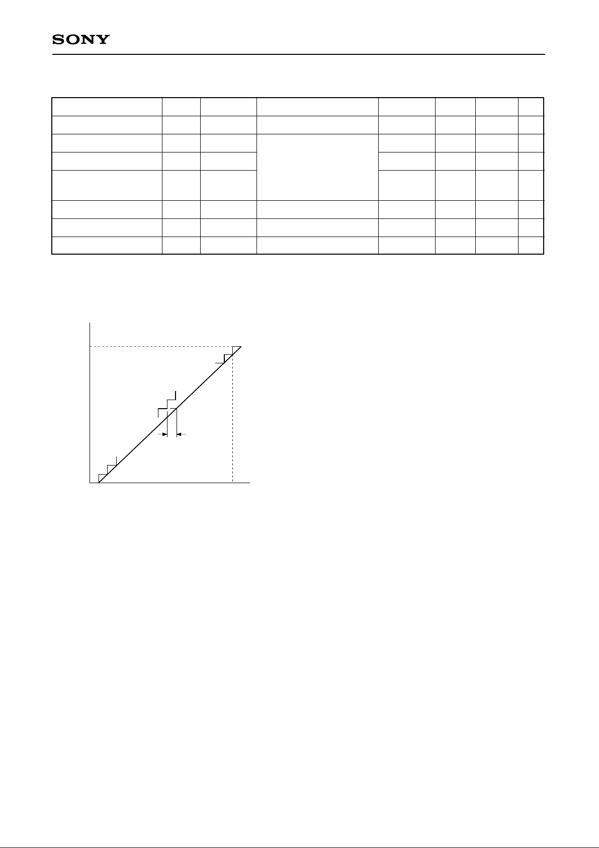
(3) A/D converter characteristics (Ta = –20 to +75°C, VDD = 4.5 to 5.5V, Vss = 0V)
Item Symbol Pin
Resolution
Linearity error
∗1
Zero transition voltage
Full-scale transition
voltage
Conversion time
Sampling time
Analog input voltage
VZT
∗2
VFT
tCONV
tSAMP
VIAN
AN0 to AN7
Fig. 6. Definition of A/D converter terms
FFH
FEH
Digital conversion value
Linearity error
Condition Min.
A/D converter operation
only
Ta = 25°C
VDD = 5.0V
VSS = 0V
∗1
VZT : Digital Value converted between 00H to 01H.
∗2
VFT : Digital Value converted between FEH and FFH.
∗3
fADC :ADC operation clock selection (MSC: Bit 0 of
address 01FFH) and assumes following values:
fADC = fc/2 when PS2 is selected.
fADC = fc when PS1 is selected.
–10
4930
160/fADC
12/fADC
0
∗3
∗3
Typ.
70
5050
Max. Unit
Bits
8
±3
150
5120
LSB
mV
mV
µs
µs
VDD
V
01H
00
H
VZT VFT
Analog input
– 17 –
Page 18
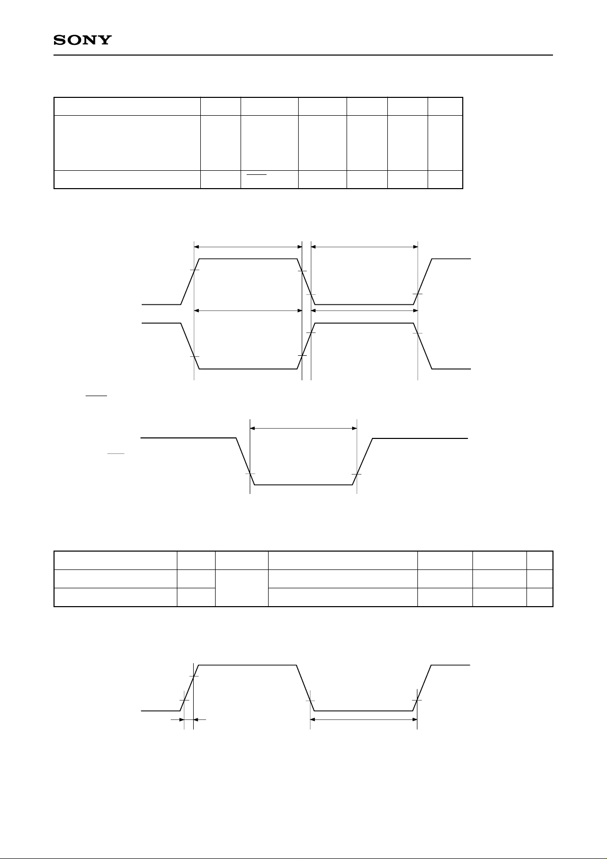
(4) Interrupts, reset inputs (Ta = –20 to +75°C, VDD = 4.5 to 5.5V, Vss = 0V)
Item Symbol Pin Condition Min. Max. Unit
INT0
External interrupt High and
Low level widths
tIH
tIL
INT1
INT2
1
µs
INT3
Reset input Low level width
tRSL
RST
8/fc
µs
Fig. 7. Interrupt input timing
tIH tIL
0.8VDD
CXP82532/82540
INT0
INT1
INT2
INT3
0.2VDD
tIL tIH
Fig. 8. RST input timing
RST
0.2VDD
(5) Power-on reset
Power-on reset
∗
Item Symbol Pin
Power supply rising time
tR
VDD
Power supply cut-off time
∗
Specifies only when power-on reset function is selected.
tOFF
Power-on reset
Repetitive power-on reset
tRSL
(Ta = –20 to +75°C, VDD = 4.5 to 5.5V, VSS = 0V)
Condition Min.
0.2VDD
0.8VDD
0.05
1
Max. Unit
50
ms
ms
Fig. 9. Power-on reset
DD
V
4.5V
0.2V 0.2V
tOFFtR
The power supply should be rise smoothly.
– 18 –
Page 19

Supplement
A
A
Fig. 10. Recommended Oscillation Circuit
CXP82532/82540
(i)
EXTAL
AAA
C
1 C2
Manufacturer
MURATA MFG
CO., LTD
XTAL
Model fc (MHz)
CSA4.19MG
CSA8.00MG
CSA10.0MT
CST4.19MGW
CST8.00MTW
CST10.00MTW
(ii)
EXTAL
AAA
4.19
8.00
10.00
∗
∗
4.19
8.00
∗
10.00
C1
XTAL
C2
C1 (pF) C2 (pF)
30
Circuit
Example
(i)
30
(ii)
4.19
FUJI SANGYO
CO., LTD
KINSEKI LTD.
∗
Indicates types with on-chip grounding capacitors (C1 and C2).
HC-49/U03
HC-49/U (-S)
8.00
10.00
4.19
8.00
10.00
15
27
15
(i)
27
– 19 –
Page 20
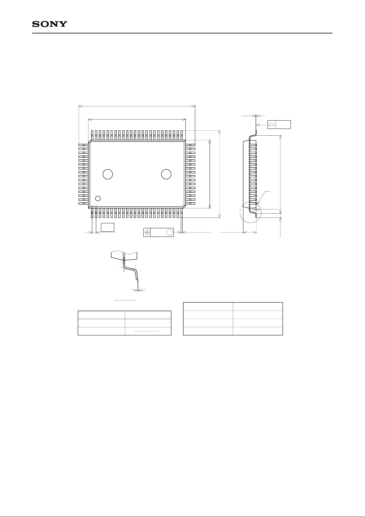
Package Outline Unit: mm
CXP82532/82540
80PIN QFP (PLASTIC)
23.9 ± 0.4
+ 0.4
20.0 – 0.1
64
65
41
40
+ 0.4
17.9 ± 0.4
14.0 – 0.1
+ 0.1
0.15 – 0.05
0.15
16.3
A
80
1
0.8
0.12
M
24
0.35 – 0.1
25
+ 0.15
+ 0.35
2.75 – 0.15
+ 0.2
0.1 – 0.05
0.8 ± 0.2
SONY CODE
EIAJ CODE
JEDEC CODE
0° to 10°
DETAIL A
QFP-80P-L01
QFP080-P-1420
PACKAGE STRUCTURE
PACKAGE MATERIAL
LEAD TREATMENT
LEAD MATERIAL
PACKAGE MASS
EPOXY RESIN
SOLDER PLATING
42/COPPER ALLOY
1.6g
– 20 –
 Loading...