

Page 1
CMOS 4-bit Single Chip Microcomputer
Description
The CXP5084/5086 is a CMOS 4-bit microcomputer
which consists of 4-bit CPU, ROM, RAM, I/O port,
8-bit timer, 8-bit timer/counter, 18-bit time base timer,
8-bit serial I/O, vector interruption, power on reset
function and a liquid crystal displayer (LCD) controller/
driver. They are integrated into a single clip with the
standby function etc. which are to be operated at low
power consumption.
Features
• Instruction cycle 3.8µs/4.19MHz
1.9µs/4.19MHz
(High speed version)
• ROM capacity 4096 × 8 bits (CXP5084)
6144 × 8 bits (CXP5086)
• RAM capacity 400 × 4 bits
(Including stack, display area)
• 32 general purpose I/O ports
• LCD controller/driver (Direct drive possible)
— Optional specification of 24, 20 or 16 segment outputs
— 1/2, 1/3, 1/4 duty selectable through program
— 1/3 bias
• 2 external interruption input pins
• 8-bit/4-bit variable serial I/O
• 8-bit timer, 8-bit timer/event counter and 18-bit time
base timer are independently controllable
• Arithmetic and logical operations possible between
the entire RAM area, I/O area and the accumulator
by means of memory mapped I/O
• Reference to the entire ROM area is possible with
the table look-up instruction
• 2 types of power down modes: sleep and stop
• Power on reset circuit (Mask option)
• Available option of either crystal oscillation or CR
oscillation (mask option) types for the oscillation
circuit
• 64-pin plastic SDIP/QFP available
• Piggyback package (CXP5080) available
Structure
Silicon gate CMOS IC
– 1 –
E90377A7Z-PS
Sony reserves the right to change products and specifications without prior notice. This information does not convey any license by
any implication or otherwise under any patents or other right. Application circuits shown, if any, are typical examples illustrating the
operation of the devices. Sony cannot assume responsibility for any problems arising out of the use of these circuits.
CXP5084/5086
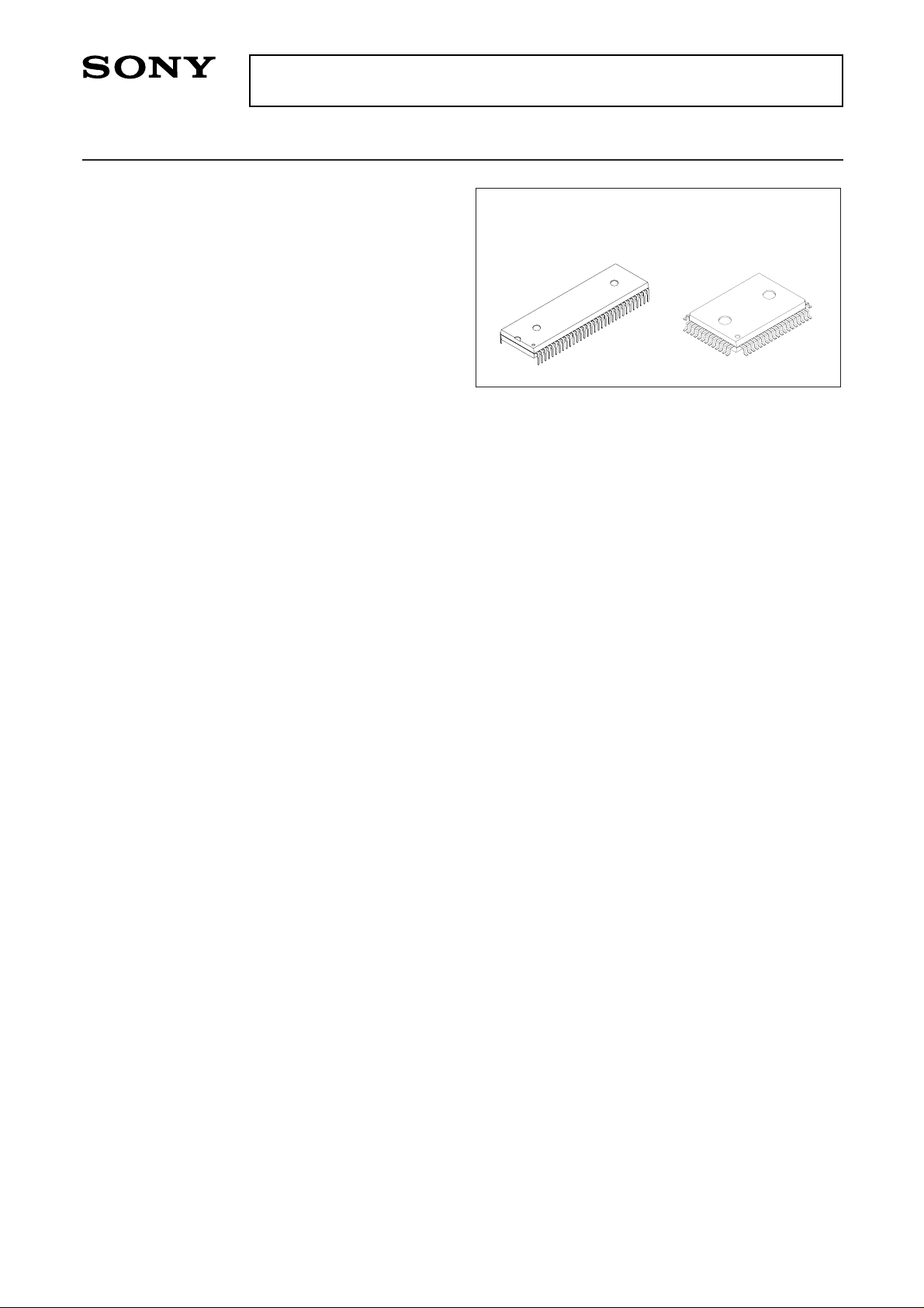
64 pin SDIP (Plastic) 64 pin QFP (Plastic)
For the availability of this product, please contact the sales office.
Page 2
– 2 –
CXP5084/5086
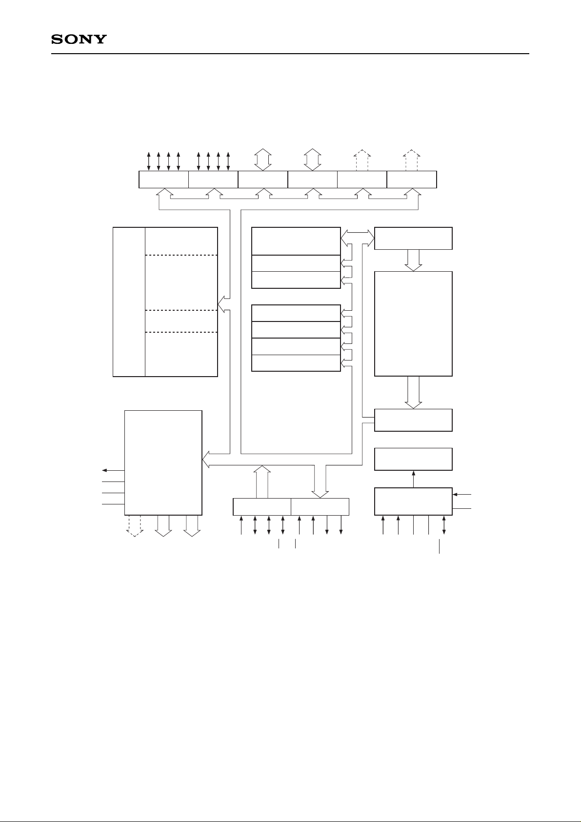
Block Diagram
4
4
ALU
V
L
VLC1
EXTAL
SEG16
to
SEG23
XTAL
V
LC3
VLC2
4
Port FPort D
Accumulator
Flag
Timer (8)
Timer/Counter (8)
Serial I/O (8)
Register
Data memory
Stack
Data memory
Interrupt control
Port EPort CPort BPort A
(Enables to specify
the I/O with bit unit)
(Combines use of mask
with segment output, optional)
(Enable to specify
the I/O with port unit)
Program counter
(13)
6144 × 8 bits
(CXP5086)
Time base timer
(18)
LCD
controller/driver
4096 × 8 bits
(CXP5084)
400 × 4
bits
Program memory
Clock contorl
Instruction control
Port YPort X
(Common with Port E, Port F)
(Common with serial I/O)
8 16 4
4
SEG0
to
SEG15
COM0
to
COM3
PX3/SI
PX2/SOA
PX1/SOB
PX0/SC
PY3/EC
PY2/INT2
PY1
PY0
INT1
V
DD
WP
VSS
RST
Page 3

– 3 –
CXP5084/5086
Pin Assignment 1 (Top View) 64-pin SDIP Package
Note) Do not make any connection to NC pin.
1
2
3
4
5
6
7
8
9
10
11
12
13
14
15
16
17
18
19
20
21
22
23
24
25
26
27
28
29
30
31
32
33
34
35
36
37
38
39
40
41
42
43
44
45
46
47
48
49
50
51
52
53
54
55
56
57
58
59
60
61
62
63
64
V
L
XTAL
EXTAL
RST
WP
INT1
PY0
PY1
PY2/INT2
PY3/EC
PX0/SC
PX1/SOB
PX2/SOA
PX3/SI
PD0
PD1
PD2
PD3
PC0
PC1
PC2
PC3
PB0
PB1
PB2
PB3
PA0
PA1
PA2
PA3
NC
V
SS
SEG5
SEG6
SEG7
SEG8
SEG9
SEG10
SEG11
SEG12
SEG13
SEG14
SEG15
SEG16/PF0
SEG17/PF1
SEG18/PF2
SEG19/PF3
SEG20/PE0
SEG21/PE1
SEG22/PE2
SEG23/PE3
VDD
VLC3
VLC2
VLC1
COM0
COM1
COM2
COM3
SEG0
SEG1
SEG2
SEG3
SEG4
Page 4
– 4 –
CXP5084/5086
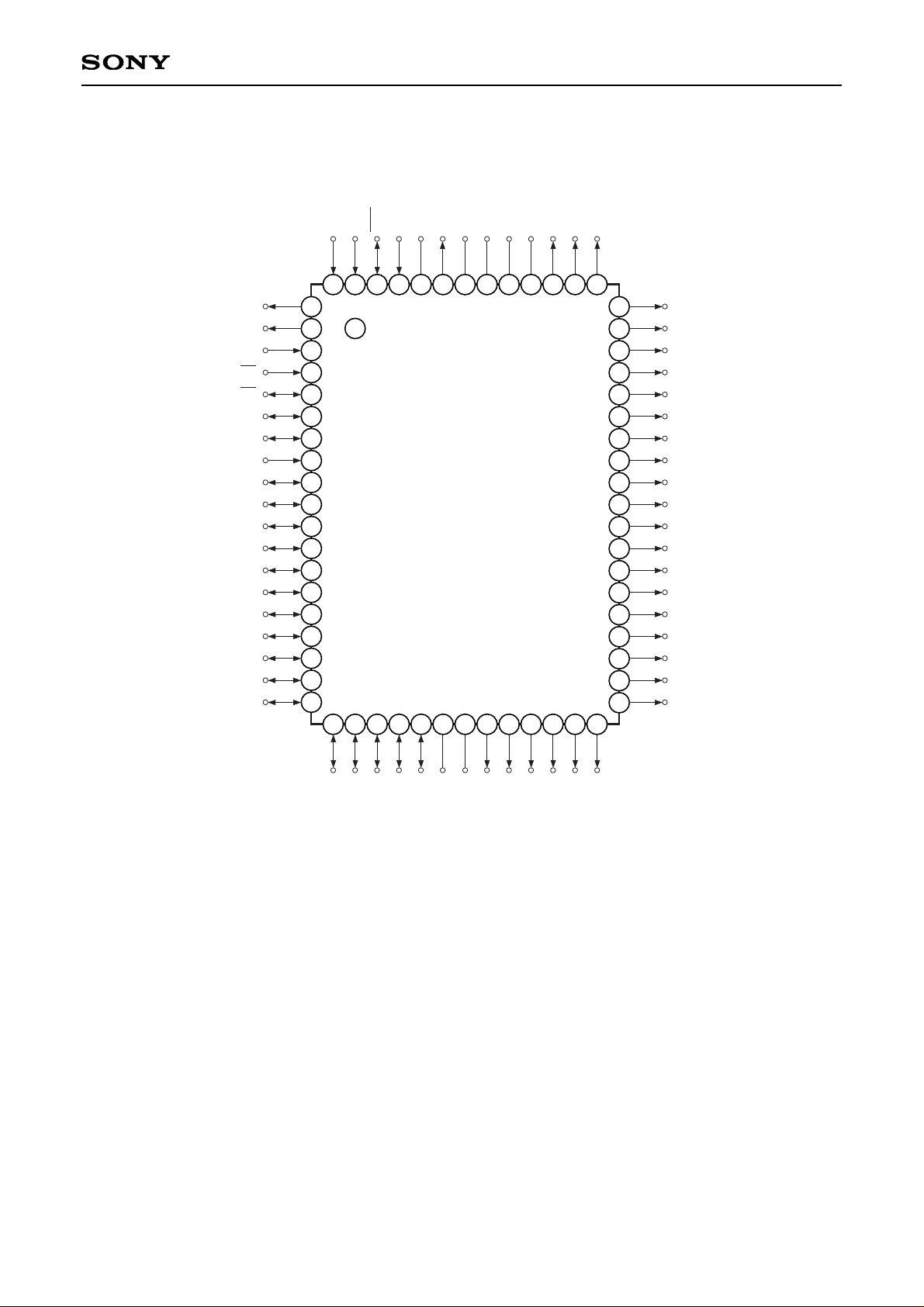
Pin Assignment 2 (Top View) 64-pin QFP Package
Note) Do not make any connection to NC pin.
1
2
3
4
5
6
7
8
9
10
11
12
13
14
15
16
17
18
19
20 21 22 23 24 25 26 27 28 29 30 31 32
33
34
35
36
37
38
39
40
41
42
43
44
45
46
47
48
49
50
51
52535455565758596061626364
PY0
PY1
PY2/INT2
PY3/EC
PX0/SC
PX1/SOB
PX2/SOA
PX3/SI
PD0
PD1
PD2
PD3
PC0
PC1
PC2
PC3
PB0
PB1
PB2
PB3
PA0
PA1
PA2
PA3
V
SS
NC
SEG23/PE3
SEG22/PE2
SEG21/PE1
SEG20/PE0
SEG19/PF3
SEG18/PF2
INT1
WP
RST
EXTAL
XTAL
V
L
VDD
VLC3
VLC2
VLC1
COM0
COM1
COM2
COM3
SEG0
SEG1
SEG2
SEG3
SEG4
SEG5
SEG6
SEG7
SEG8
SEG9
SEG10
SEG11
SEG12
SEG13
SEG14
SEG15
SEG16/PF0
SEG17/PF1
Page 5

– 5 –
CXP5084/5086
Absolute Maximum Ratings
Item
Power supply voltage
LCD bias voltage
Input voltage
Output voltage
High level output current
High level total output current
Low level output current
Low level total output current
Operating temperature
Storage temperature
Allowable power dissipation
VDD
VLC1, VLC2, VLC3
VIN
VOUT
IOH
∑IOH
IOL
∑IOL
Topr
Tstg
PD
–0.3 to +7.0
–0.3 to +7.0
∗1
–0.3 to +7.0
∗1
–0.3 to +7.0
∗1
–5
–50
15
50
–20 to +75
–55 to +150
1000
600
V
V
V
V
mA
mA
mA
mA
°C
°C
mW
mW
General purpose port∗2: per pin
Entire pin total
General purpose port∗2: per pin
Entire pin total
SDIP
QFP
Symbol Ratings Unit Remarks
∗1
VLC1, VLC2, VLC3, VIN and VOUT should not exceed VDD + 0.3V.
∗2
The PE and PF are specified when PA to PD, PX0 to PX2, PY0, PY1 and mask option are selected as the port.
Note) Usage exceeding absolute maximum ratings may permanently impair the LSI. Normal operation should
better take place under the recommended operating conditions. Exceeding those conditions may
adversely affect the reliability of the LSI.
Item
Power supply voltage VDD
VLC1,
VLC2,
VLC3
VIH
VIHS
VIHEX
VIL
VILS
VILEX
Topr
LCD bias voltage
High level input voltage
Low level input voltage
Operating temperature
Symbol Min.
4.5
3.5
VSS
0.7VDD
0.8VDD
VDD – 0.4
0
0
–0.3
–20
5.5
5.5
VDD
VDD
VDD
VDD + 0.3
0.3VDD
0.2VDD
0.4
+75
V
V
V
V
V
V
V
V
V
°C
Guaranteed range during operation
Guaranteed data hold operation range
during stop
Liquid crystal power supply voltage
∗1
Hysteresis input
∗2
EXTAL pin
∗3
Hysteresis input
∗2
EXTAL pin
∗3
Max. Unit Remarks
∗1
The optimum value is determined by the characteristics of the liquid crystal display element used.
∗2
They are the respective pins of INT1, WP, PX0, PX3, PY2, PY3 and RST.
∗3
Specified only during external clock input.
Recommended Operating Conditions (VSS = 0V reference)
(Ta = –20 to +75°C, VSS = 0V reference)
Page 6

– 6 –
CXP5084/5086
Electrical Characteristics
DC characteristics (Ta = –20 to +75°C, VSS = 0V reference)
Item
High level
output voltage
VOH
PA to PF∗1,
PX0 to PX2,
PY0, PY1,
VL (VOL only)
RST (VOL only)
VDD = 4.5V, IOH = –0.5mA
∗2
VDD = 4.5V, IOH = –1.0mA
∗2
VDD = 4.5V, IOH = –10µA
∗3
VDD = 4.5V, IOH = –200µA
∗3
VDD = 4.5V, IOL = 1.8mA
VDD = 4.5V, IOL = 3.6mA
VDD = 5.5V, VIH = 5.5V
VDD = 5.5V, VIL = 0.4V
4.0
3.5
4.0
2.4
0.5
–0.5
–1.5
3
5
1.3
(2)
∗9
0.4
(0.5)
∗9
10
0.4
0.6
40
–40
–400
–2.0
±10
5
15
4
(6)
∗9
1.2
(2)
∗9
10
20
V
V
V
V
V
V
µA
µA
µA
mA
µA
kΩ
kΩ
mA
mA
µA
pF
VDD = 5.5V
VI = 0, 5.5V
VDD = 5V
VLC1 = 3.75V
VLC2 = 2.5V
VLC3 = 1.25V
VDD = 5.5V During external clock
1MHz operation
Entire output pins open
Clock 1MHz
0V for no measured pins
Sleep mode
Stop mode
EXTAL
∗4
RST
∗5
PA to PF∗6,
PX0 to PX2∗6,
PX3∗8, PY0∗7,
PY1∗7, PY2∗8,
PY3∗8, INT1∗8,
WP∗8, RST
∗5
COM0 to COM3
SEG0 to SEG15
SEG16 to SEG23
∗1
VDD
VLC1 to VLC3,
COM0 to COM3,
SEG0 to SEG15,
SEG16 to SEG23∗1,
Other pins than VDD,
VSS
VOL
IIH
IILE
IILR
IIL
IIZ
RCOM
RSEG
IDD
IDDSP
IDDS
CIN
Low level
output voltage
Input current
High impedance
I/O leakage current
Common output
impedance
Segment output
impedance
Current power
supply
Input capacitance
Symbol Pin Condition Min. Typ. Max. Unit
∗1
PE to PF show when the combined pins are selected as the port, and SEG16 to SEG23 show when the
combined pins are selected as the segment output.
∗2
It is when the respective pins of PA to PF and PX0 to PX2 select the 3-state output circuit, and PY0 and
PY1 are when the inverter output circuit is selected.
∗3
It is when the respective pins of PA to PF, PX0 to PX2, PY0 and PY1 select the pull-up resistance.
∗4
It is when the crystal or ceramic oscillation circuit is selected.
∗5
The RST pin specifies the input current when the pull-up resistance is selected, and specifies leakage
current when non-resistance is selected.
∗6
The respective pins of PA to PF and PX0 to PX2 specify the input current when the pull-up resistance is
selected, and specify the leakage current when in the port state during the 3-state output circuit or standby
is selected at high impedance.
∗7
The respective pins of PY0 and PY1 specify the input current when the pull-up resistance is selected, and
specify the leakage current when the port state during standby is selected at high impedance.
∗8
The respective pins of PX3, PY2, PY3, INT1 and WP only specify the leakage current.
∗9
The value in parentheses shows the specification of the current power supply of the high speed version.
Page 7

– 7 –
CXP5084/5086
AC characteristics
(1) Clock timing (Ta = –20 to +75°C, VDD = 4.5 to 5.5V, VSS = 0V reference)
Item
System clock frequency
System clock input pulse width
System clock input rising and falling
times
Event count clock input pulse width
Event count clock input rising and
falling times
fc
tXL
tXH
tCR
tCF
tEL
tEH
tER
tEF
XTAL
EXTAL
EXTAL
EXTAL
EC
EC
Fig. 1., Fig. 2.
Fig. 1., Fig. 2.
∗1
External clock drive
Fig. 1., Fig. 2.
∗1
External clock drive
Fig. 3.
Fig. 3.
1
90
tsys
∗2
+ 0.05
5
200
20
MHz
ns
ns
µs
ms
Symbol Pin Condition Min. Max. Unit
∗1
The external clock in Fig. 2. is specified only when the option is selected for crystal or ceramic oscillation.
∗2
In the standard version, tsys = 16/fc
In the high speed version, tsys = 8/fc
Note) When adjusting the frequency accurately, there may be cases in which they differ from Fig. 2.
EXTAL
1/fc
t
XH tCF tXL tCR
VDD – 0.4V
0.4V
Fig. 2. Clock applying condition
Crystal oscillation
Ceramic oscillation
CR oscillation External clock
∗1
EXTAL XTAL
C1 C2
EXTAL XTAL
R
C
EXTAL XTAL
OPEN
Fig. 3. Event count clock timing
EC
t
EH tEF tEL tER
0.8VDD
0.2V
Fig. 1. Clock timing
Page 8
– 8 –
CXP5084/5086
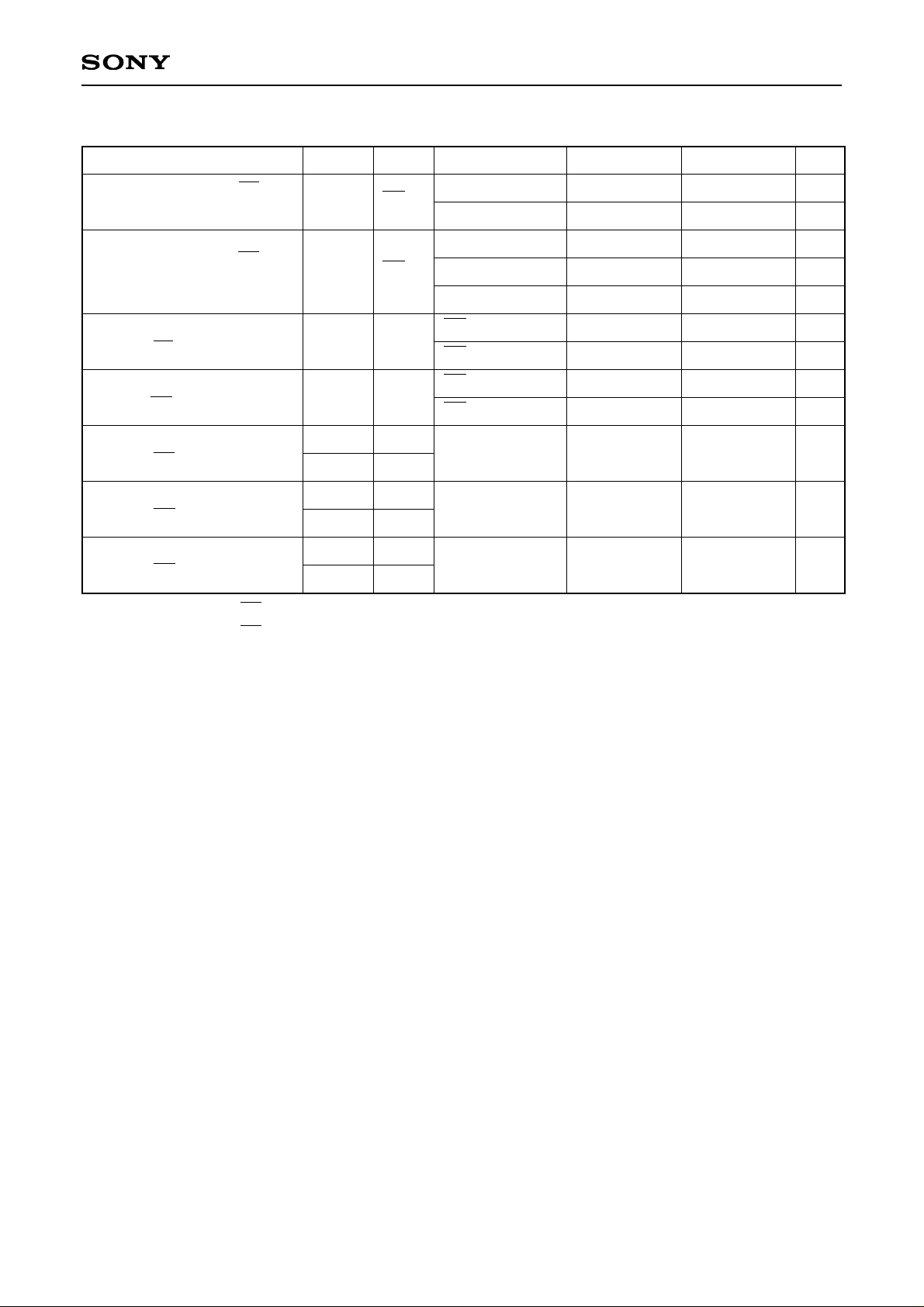
(2) Serial transfer (Ta = –20 to +75°C, VDD = 4.5 to 5.5V, VSS = 0V reference)
Item
Serial transfer clock (SC)
cycle time
tKCY
tKH
tKL
tSIK
tKSI
tKSOA
tKSOB
tKSOA
tKSOB
tKSOA
tKSOB
SC
Input mode
Output mode
Input mode
Output mode
∗1
Output mode
∗2
SC input mode
SC output mode
SC input mode
SC output mode
tsys/4 + 1.42
tsys
tsys/8 + 0.7
tsys/2 – 0.1
tsys/2 – 1.6
0.1
0.2
tsys/8 + 0.5
0.1
tsys/8 + 0.5
tsys/8 + 1.6
tsys/8 + 0.5
µs
µs
µs
µs
µs
µs
µs
µs
µs
µs
µs
µs
SC
SI
SI
SOA
SOB
SOA
SOB
SOA
SOB
Serial transfer clock (SC)
high and low level widths
Serial data input setup time
(against SC ↑)
Serial data input hold time
(against SC ↑)
High data∗3output delay time
from the SC falling time
High data∗4output delay time
from the SC falling time
Low data output delay time
from the SC falling time
Symbol Pin Condition Min. Max. Unit
∗1
It is specified when SC pin is selected to the 3-state output by the mask option.
∗2
It is specified when SC pin is selected to the pull-up resistance by the mask option. As the tsys receives
restriction by this item, take notice that it limits the upper limit of the system clock frequency fc.
∗3
It is specified when SOA and PX1/SOB pins are selected to the 3-state output by the mask option.
∗4
It is specified when SOA and PX1/SOB pins are selected to the pull-up resistance by the mask option.
Note 1) In the standard version, tsys = 16/fc
In the high speed version, tsys = 8/fc
Note 2) The load of data output delay time is 50pF + 1TTL.
Page 9

– 9 –
CXP5084/5086
tKCY
0.8VDD
0.8VDD
0.2VDD
0.2VDD
0.8VDD
0.2VDD
tKL
tSIK
tKSOA
tKSOB
tKSI
tKH
SC
SI
SOA
SOB
Input data
Output data
Fig. 4. Serial transfer timing
(3) Others (Ta = –20 to +75°C, VDD = 4.5 to 5.5V, VSS = 0V reference)
Item
External interruption high and
low level widths
tI1H, tI1L
tI2H, tI2L
tRSL
tWPH
INT1
INT2
RST
WP
During edge detection mode
Stop mode
Sleep mode
µs
µs
µs
ns
µs
tsys + 0.05
tsys + 0.05
2tsys
500
tsys + 0.05
Reset input low level width
Wake-up input high level width
Symbol Pin Condition Min. Max. Unit
Note) In the standard version, tsys = 16/fc
In the high speed version, tsys = 8/fc
Page 10

– 10 –
CXP5084/5086
Fig. 5. Interruption input timing
INT1
(Falling edge)
0.2V
DD
0.2VDD
INT1
(Rising edge)
t
I1H
tI1L
tI1L
tI1H
0.8VDD
0.8VDD
0.2VDD
INT2
tI2L
tI2H
0.8VDD
Fig. 6. Reset input timing
0.2VDD
RST
tRSL
Fig. 7. Wake-up input timing
0.8VDD
WP
t
WPH
Power supply rising time
Power supply cut-off time
tR
tOFF
VDD
Power on reset
Repectitive power on reset
0.05
1
50 ms
ms
Item Symbol Pin Condition Min. Max. Unit
Power on reset
∗
(Ta = –20 to +75°C, VSS = 0V reference)
∗
Specifies only when power on reset function is selected.
Fig. 8. Power on reset
VDD
tR tOFF
0.2V0.2V
4.5V
Raise the power supply smoothly.
Page 11

PACKAGE STRUCTURE
PACKAGE MATERIAL
LEAD TREATMENT
LEAD MATERIAL
PACKAGE MASS
SONY CODE
EIAJ CODE
JEDEC CODE
SDIP-64P-01
42 ALLOY
SOLDER PLATING
EPOXY RESIN
64PIN SDIP (PLASTIC)
SDIP064-P-0750
57.6 – 0.1
+ 0.4
64
33
1 32
1.778
19.05
17.1 – 0.1
+ 0.3
0° to 15°
0.25 – 0.05
+ 0.1
0.5 MIN
4.75 – 0.1
+ 0.4
3.0 MIN
0.5 ± 0.1
0.9 ± 0.15
8.6g
– 11 –
CXP5084/5086
Package Outline Unit: mm
SONY CODE
EIAJ CODE
JEDEC CODE
23.9 ± 0.4
20.0 – 0.1
0.4 – 0.1
+ 0.15
14.0 – 0.1
1
19
20
32
33
51
52
64
0.15 – 0.05
+ 0.1
2.75 – 0.15
16.3
0.1 – 0.05
+ 0.2
0.8 ± 0.2
M
0.2
0.15
+ 0.4
17.9 ± 0.4
+ 0.4
+ 0.35
64PIN QFP(PLASTIC)
QFP-64P-L01
QFP064-P-1420
PACKAGE MATERIAL
LEAD TREATMENT
LEAD MATERIAL
PACKAGE MASS
EPOXY RESIN
SOLDER/PALLADIUM
42/COPPER ALLOY
PACKAGE STRUCTURE
PLATING
1.5g
1.0
0° to10°
 Loading...