

Page 1
CXP5080
CMOS 4-bit Single Chip Microcomputer
Description
CXP5080 is a CMOS 4-bit single chip microcomputer
of piggyback/evaluator combined type which has
been developed for functional evaluation of the
CXP5084/5086.
Features
• Instruction cycle 3.8µs/4.19MHz (CXP5080)
1.9µs/4.19MHz (CXP5080H)
• ROM capacity Maximum 8K bytes (EPROM 27C64, LCC/DIP type 27C64)
• RAM capacity 400 × 4 bits (Including stack, display area)
• 32 general purpose I/O ports
• 16 large current output ports
• LCD controller/driver (Enables to direct drive)
— Enables to specify the segment output of 24, 20 and 16 optionally
— Enables to select program of the duty, 1/2, 1/3 and 1/4
— 1/3 bias
• 2 external interruption input pins
• 8-bit timer, 8-bit timer/event counter and 18-bit time base timer, independently controlled
• Arithmetic and logical operations possible between the entire RAM area, l/O area and the accumulator by
means of memory mapped I/O
• Reference to the entire ROM area is possible with the table look-up instruction
• 2 kinds of power down modes of sleep and stop
• Power on reset circuit (mask option)
• The oscillation circuit may be optionally specified as the crystal oscillation type or the CR oscillation type
• 64-pin ceramic SDIP/QFP
Note) Mask options are determined according to the CXP5080 category.
For details refer to the product list.
Structure
Silicon gate CMOS IC
– 1 –
E61113A7Z-PS
Sony reserves the right to change products and specifications without prior notice. This information does not convey any license by
any implication or otherwise under any patents or other right. Application circuits shown, if any, are typical examples illustrating the
operation of the devices. Sony cannot assume responsibility for any problems arising out of the use of these circuits.
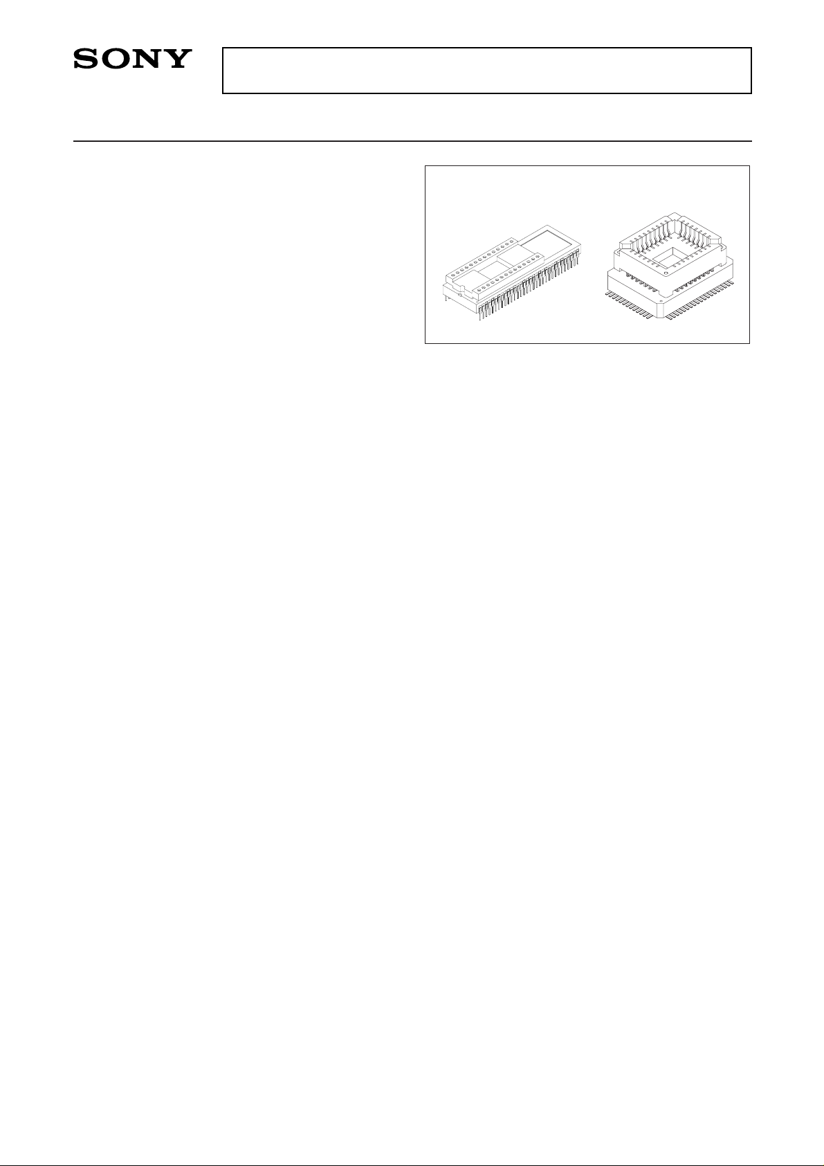
64 pin PSDIP (Ceramic) 64 pin PQFP (Ceramic)
Piggyback/
evaluator type
For the availability of this product, please contact the sales office.
Page 2

– 2 –
CXP5080
ALU
VL
VLC1
EXTAL
SEG16
SEG23
XTAL
V
LC3
VLC2
13
8
Accumulator
Flag
Timer (8)
Timer/counter (8)
Serial I/O (8)
Register
Data memory
Stack
Data memory
Interruption control
Port A Port B Port C Port D Port E Port F
(Enables to specify
the I/O with bit unit)
(Enables to specify
the I/O with port unit)
(Combined use of mask
with segment output, optional.)
Program
counter (13)
A0 to A12
I0 to I7
Time base timer (18)
LCD
controller/driver
Instruction
input buffer
400 × 4
bits
Address buffer
Clock control
Instruction control
Port YPort X
(Combined use of serial I/O)
16 4
to to to
SEG0
SEG15
COM0
COM3
PX3/SI
PX2/SOA
PX1/SOB
PX0/SC
PX3/EC
PY2/INT2
PY1
PY0
INT1
V
DD
WP
VSS
RST
4
4 44
8
Block Diagram
Page 3
– 3 –
CXP5080
1
2
3
4
5
6
7
8
9
10
11
12
13
14
1
2
3
4
5
6
7
8
9
10
11
12
13
14
15
15
16
16
17
17
18
18
19
19
20
20
21
21
22
22
23
23
24
24
25
25
26
26
27
27
28
28
29
30
31
32
33
34
35
36
37
38
39
40
41
42
43
44
45
46
47
48
49
50
51
52
53
54
55
56
57
58
59
60
61
62
63
64
V
L
XTAL
EXTAL
RST
WP
INT1
PY0
PY1
PY2/INT2
PY3/EC
PX0/SC
PX1/SOB
PX2/SOA
PX3/SI
PD0
PD1
PD2
PD3
PC0
PC1
PC2
PC3
PB0
PB1
PB2
PB3
PA0
PA1
PA2
PA3
PESEL
V
SS
SEG5
SEG6
SEG7
SEG8
SEG9
SEG10
SEG11
SEG12
SEG13
SEG14
SEG15
SEG16/PF0
SEG17/PF1
SEG18/PF2
SEG19/PF3
SEG20/PE0
SEG21/PE1
SEG22/PE2
SEG23/PE3
VDD
VLC3
VLC2
VLC1
COM0
COM1
COM2
COM3
SEG0
SEG1
SEG2
SEG3
SEG4
VSS
VDD
A12
A7
A6
A5
A4
A3
A2
A1
A0
I0
I1
I2
I3
V
DD
VDD
VDD
A8
A9
A11
V
SS
A10
V
SS
I7
I6
I5
I4
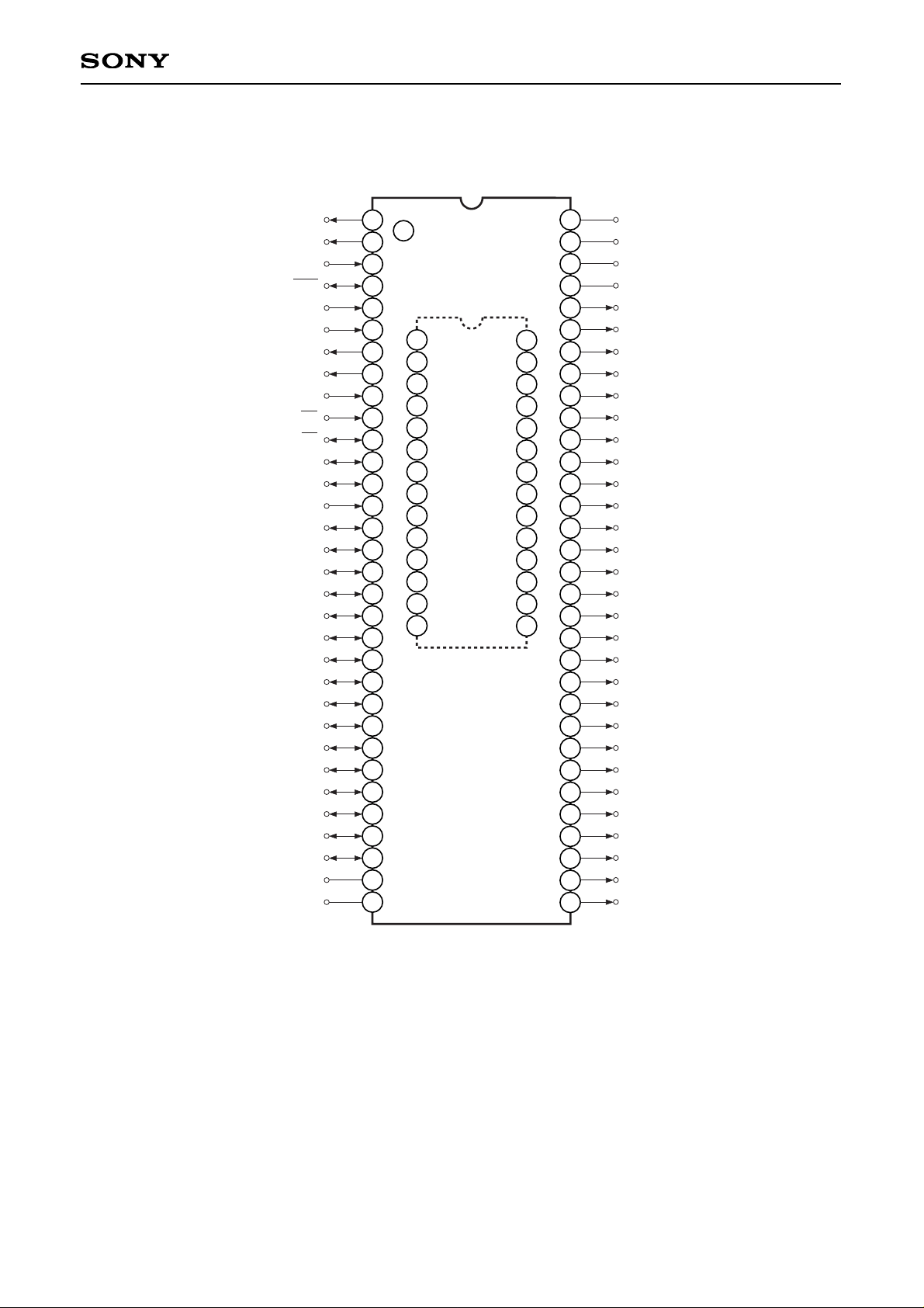
Pin Assignment 1 (Top View) 64 pin PSDIP Package
Note) PESEL pin serves to switch the I/O signal of the socket on top of the package from interface with the
evaluator (Eva mode) to interface with EPROM (Piggyback mode).
Setting PESEL pin to H Ievel brings Eva mode to enable the connection with the evaluator. Setting it to
L level brings piggyback mode to enable the mounting of EPROM. For QFP piggyback, it is necessary
only to exchange EVACAP (or EPROM) for EPROM (or EVACAP) and no other special measures are
required.
Page 4

– 4 –
CXP5080
1
122
3
3
4
4
5
6
7
8
9
10
11
12
13
5
6
7
8
9
10
11
12
13
14
14151516161717181819192020
2121222223232424252526262727282829293030313132
32
33
34
35
36
37
38
39
40
41
42
43
44
45
46
47
48
49
50
51
52535455565758596061626364
PY0
PY1
PY2/INT2
PY3/EC
PX0/SC
PX1/SOB
PX2/SOA
PX3/SI
PD0
PD1
PD2
PD3
PC0
PC1
A6
A5
A4
A3
A2
A1
A0
NC
I0
PC2
PC3
PB0
PB1
PB2
PB3
PA0
PA1
PA2
PA3
V
SS
NC
I1
I2
V
SS
NC
I3
I4
I5
SEG23/PE3
SEG22/PE2
SEG21/PE1
SEG20/PE0
SEG19/PF3
SEG18/PF2
INT1
WP
RST
EXTAL
XTAL
V
L
VDD
A7
A12
VDDPESEL
VDDVDD
PESEL
V
LC3
VLC2
VLC1
COM0
COM1
COM2
COM3
SEG0
SEG1
SEG2
SEG3
SEG4
SEG5
SEG6
SEG7
SEG8
SEG9
SEG10
SEG11
SEG12
SEG13
SEG14
A8
A9
A11
NC
V
SS
A10
V
SS
I7
I6
SEG15
SEG16/PF0
SEG17/PF1
Pin Assignment 2 (Top View) 64 pin PQFP Package
Note 1) PESEL pin serves to switch the I/O signal of the socket on top of the package from interface with the
evaluator (Eva mode) to interface with EPROM (Piggyback mode).
Setting PESEL pin to H Ievel brings Eva mode to enable the connection with the evaluator. Setting it to
L level brings piggyback mode to enable the mounting of EPROM. For QFP piggyback, it is necessary
only to exchange EVACAP (or EPROM) for EPROM (or EVACAP) and no other special measures are
required.
Note 2) Do not make any connections to NC pin.
Page 5

– 5 –
CXP5080
EPROM read timing
(Ta = –20 to +75°C, VDD = 4.5 to 5.5V, VSS = 0V reference)
Item
Symbol
tACC
tIH
Pin
A0 to A12
I0 to I7
A0 to A12
I0 to I7
Unit
ns
300
0 ns
Min. Max.
Address → Data
input delay time
Address → input
holding time
tACC
tIH
0.8VDD
A0 to A12
I0 to I7
0.2VDD
Address data
0.8V
DD
0.2VDD
Input data
Products List
Optional item
Package
ROM capacity
Speed
Oscillation type
64-pin plastic
SDIP/QFP
6K byte
Standard/High speed
Crystal/CR
Segment output
Output type
PY0 and PY1
output type
Output state during
standby
Pull-up resistance
of reset pin
16/20/24
Tri-state/
Pull-up resistance/
Open drain
Pull-up resistance/
Inverter
Holding state/Hi-Z
Existent/non-existent
Incorporated power
on reset circuit
SOA pin output
SOB pin output
Existent/non-existent
Normal/Input
Normal/Input
64-pin ceramic
PSDIP/PQFP
EPROM 8K byte
High speed
Crystal
20
Tri-state
Pull-up resistance
Hi-Z
Existent
Existent
Input
Normal
64-pin ceramic
PSDIP/PQFP
EPROM 8K byte
High speed
Crystal
24
Tri-state
Pull-up resistance
Hi-Z
Existent
Existent
Input
Normal
64-pin ceramic
PSDIP/PQFP
EPROM 8K byte
High speed
Crystal
16
Tri-state
Pull-up resistance
Hi-Z
Existent
Existent
Input
Normal
Mask ROM
CXP5086
CXP5080HU02AS
CXP5080HU02AQ
CXP5080HU03AS
CXP5080HU03AQ
CXP5080HU04AS
CXP5080HU04AQ
Note) All of the above products are combined chips of piggyback and evaluator.
Page 6

– 6 –
CXP5080
Package Outline Unit: mm
64PIN PSDIP (CERAMIC) 750mil
15.24
2.54 ± 0.25
64 33
1 32
18.76 ± 0.29
+ 0.74
57.0 – 0.53
19.05 ± 0.3
0.25 ± 0.05
0° to 9°
10.16 MAX
0.48 ± 0.1
0.9 ± 0.2
1.778 ± 0.2
1.27 ± 0.25
3.4 ± 0.3
SONY NAME PSDIP-64C-021
EIAJ NAME ADIP064-C-0750-AF
JEDEC CODE
64PIN PQFP (CERAMIC)
18.7
16.3 ± 0.2
64 52
PIN No.1 INDEX
INDEX
1
19
22.3 ± 0.3
24.7
20 32
9.48
11.66
15.58 ± 0.2
33
51
1.27 ± 01.3
12.02
14.22
18.12 ± 0.2
0.3
6.0
4.5
52
51
PIN No.1 INDEX
64
1
19
2032
33
0.7
1.0
1.51.3 ± 0.3
1.0 ± 0.05
0.4 ± 0.08
SONY NAME PQFP-64C-L01
EIAJ NAME AQFP054-C-0000-A
JEDEC CODE
3.07 ± 0.3
9.32 MAX
+ 0.05
0.15 – 0.02
 Loading...