

Page 1

CMOS-CCD 1/2H Delay Line for NTSC
Description
The CXL5002M/P are general-purpose CMOS-CCD
delay line ICs that provide 1/2H delay time for NTSC.
Features
• Low power consumption 70mW (Typ.)
• Small size package (8-pin SOP, DIP)
• Low differential gain DG = 3% (Typ.)
• Input signal amplitude 180 IRE (= 1.28Vp-p, Max.)
• Low input clock amplitude operation 150mVp-p (Min.)
• Built-in peripheral circuits (clock driver, timing
generator, autobias, and output circuits)
Functions
• 340-bit CCD register
• Clock drivers
• Autobias circuit
• Sync tip clamp circuit
• Sample and hold circuit
Structure
CMOS-CCD
Absolute Maximum Ratings (Ta = 25°C)
• Supply voltage VDD 11 V
• Supply voltage VCL 6V
•Operating temperature Topr –10 to +60 °C
• Storage temperature Tstg –55 to +150 °C
• Allowable power dissipation PD
CXL5002M 350 mW
CXL5002P 480 mW
Recommended Operating Conditions
Supply voltage VDD 9 ± 5% V
VCL 5 ± 5% V
Recommended Clock Conditions
• Input clock amplitude VCK 150mVp-p to 1.0Vp-p
(250mVp-p typ.)
• Clock frequency fCK 10.7MHz
– 1 –
E50586B79-PS
Sony reserves the right to change products and specifications without prior notice. This information does not convey any license by
any implication or otherwise under any patents or other right. Application circuits shown, if any, are typical examples illustrating the
operation of the devices. Sony cannot assume responsibility for any problems arising out of the use of these circuits.
CXL5002M/P
CXL5002M
8 pin SOP (Plastic)
CXL5002P
8 pin DIP (Plastic)
Page 2

– 2 –
CXL5002M/P
Blook Diagram
2
V
SS
V
CL
CLK
IN
AUTO
FEED
4
5
340-BIT SHIFT REGISTER
DUTY CONTROL
CIRCUIT
1
φ1
φ2
AUTO BIAS CIRCUIT
CLAMP CIRCUIT
OUT
CLOCK DRIVERS
AMP S/H AMP AMP
6
7
8
3
V
DD
ref.
(1 BIT)
φ
2φ1
Pin Description
Pin No. Symbol Description Impedance [Ω]
1
2
3
4
VSS
VCL
CLK
VDD
GND
5V power supply
Clock input
9V power supply
> 100k
Pin No. Symbol Description Impedance [Ω]
5
6
7
8
OUT
FEED
AUTO
IN
Signal output
Feedback DC output
Autobias DC output
Signal input
600 to 1k
> 100k
10k
> 100k
Page 3

– 3 –
CXL5002M/P
Electrical Characteristics
(Ta = 25°C, VDD = 9.0V, VCL = 5.0V, fCK = 10.7MHz, VCK = 250mVp-p sine wave,
See "Electrical characteristics test circuit")
Item Symbol Measuring condition
SW conditions
Measuring
point
Min. Typ. Max. Unit
1
2
mA
mA
dB
dB
%
deg
Vp-p
dB
V
V
V
V
5
9
3
—
5
5
1.28
—
6.5
6.5
3.3
3.7
4
7
0
–2.1
3
3
—
60
5.0
5.0
2.3
2.7
—
—
–3
–3.0
—
—
—
55
3.5
3.5
1.3
1.7
A1
A2
V1
V1
S
—
V2
V2
V3
V4
V5
V6
a
a
b
a
—
a
a
a
a
a
a
b, c
e
—
f
d
d
a
250kHz, 1.28Vp-p,
sine wave input
250kHz, 1.28Vp-p,
sine wave input
IG = 20 log (Output
voltage [Vp-p] /
1.28 [Vp-p])
Dissipation at 3.5MHz
in relation to 250kHz
fG = 20 log (V3.58MHz/
V250kHz) (Note 1)
5-staircase wave input
Y = 140 IRE (= 1.0Vp-p)
Measure S point with
vector scope (Note 2)
S: Input = 250kHz,
1.0Vp-p
output (Vp-p)
N: Input = DC ground
output (mVrms)
250kHz, 1.28Vp-p,
sine wave input
IDD
ICL
IG
fG
VIN-AC
S/N
VIN-AC
VAUTO-DC
VFEED-DC
VOUT-DC
Supply current
Insertion gain
Frequency
response
Differential gain
Differential phase
Allowable input
amplitude
Noise
Output DC
voltage
DG
DP
Page 4

– 4 –
CXL5002M/P
LPF
SW2
a b
V
BIAS
9V
Note 3)
A1
5V
A2
0.01µF
CLK
f
CK = 10.7MHz
VCK = 250mVp-p sine wave
0.01µF
V4
0.1µF
V5
V3
SW1
0.1µF
1MΩ
a.
b.
c.
d.
e.
f.
9V
5.1k
V6
BPF
Note 4)
V1
V2
Vector scope
S
V
SS
V
CL
CLK
V
DD
IN
AUTO
FEED
OUT
CXL5002M/P
5
6
7
8
4
2
3
1
100k
250kHz, 1.28Vp-p sine wave
250kHz, 300mVp-p sine wave
3.58MHz, 300mVp-p sine wave
5-staircase wave
Ground
250kHz, 1.0Vp-p sine wave
Electrical Characteristics Test Circuit
Page 5

– 5 –
CXL5002M/P
Note 1) Frequency response measuring condition
V3.58MHz (Output signal voltage [Vp-p] at 3.58MHz input)
V250kHz (Output signal voltage [Vp-p] at 250kHz input)
Set Pin 8 (IN) voltage [V] = VIN-DC + 640mV.
3.58MHz, 300mVp-p sine wave
250kHz, 300mVp-p sine wave
640mV (adjust with V
BIAS)
VIN-DC
[V]
Note 2) Differential gain and differential phase measuring condition
1H 63.5µs
40 IRE
140 IRE (1.0Vp-p)
Chroma 40 IRE
5-staircase wave signal
DG and DP are measured at output S point by vector scope.
Note 3) LPF frequency response
0 5.8 10.7
Frequency [MHz]
–50
–3
0
[dB]
Note 4) BPF frequency response
0 4.1M 10.7M
Frequency [Hz]
–50
–3
0
[dB]
200
50
Page 6
– 6 –
CXL5002M/P
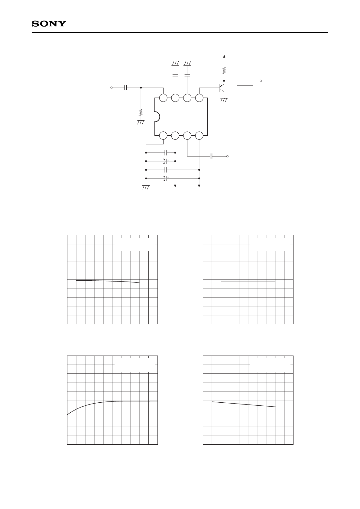
Application Circuit
L. P. F
CXL5002M/P
5V
0.01µF
CLK
f
CK = 10.7MHz
VCK = 250mVp-p sine wave
0.01µF 0.1µF
Composite video signal input
0.1µF
1MΩ
9V
5.1k
5
6
7
8
4
2
signal output
3
1
9V
0.01µF
47µF
0.01µF
47µF
2SA1175
Application circuits shown are typical examples illustrating the operation of the devices. Sony cannot assume responsibility for
any problems arising out of the use of these circuits or for any infringement of third party patent and other right due to same.
0
–1
–2
–3
f
G
– Frequency response [dB]
Frequency response vs. Ambient temperature
–20
Ta – Ambient temperature [°C]
0 20 40 60
–4
Input = 300mVp-p
3.58MHz, sine wave
0
–1
–2
–3
V
CL – Supply voltage [V]
4.7 5.0 5.3
–4
Frequency response vs. Supply voltage
Input = 300mVp-p
3.58MHz, sine wave
f
G
– Frequency response [dB]
0
–1
–2
–3
8.5
9.0 9.5
–4
VDD – Supply voltage [V]
Frequency response vs. Supply voltage
Input = 300mVp-p
3.58MHz, sine wave
f
G
– Frequency response [dB]
Ta – Ambient temperature [°C]
1
0
–1
–2
0 60
–3
–20 20 40
Input = 1.28Vp-p
250kHz, sine wave
I
G
– Insertion gain [dB]
Insertion gain vs. Ambient temperature
Example of Representative Characteristics
Page 7

– 7 –
CXL5002M/P
1
0
–1
–2
4.7 5.0 5.3
–3
4
3
2
1
–20
20 60
0
0 40
0
–2
–3
–4
10k 100k 1M
–1
4.7 5.35.0
4
3
2
1
0
8.5 9.59.0
4
3
2
1
0
0
–1
–2
–3
8.5 9.0 9.5
1
Gain [dB]
I
G
– Insertion gain [dB]
Insertion gain vs. Supply voltage
VCL – Supply voltage [V]
Input = 1.28Vp-p
250kHz, sine wave
I
G
– Insertion gain [dB]
Insertion gain vs. Supply voltage
VDD – Supply voltage [V]
Input = 1.28Vp-p
250kHz, sine wave
DG – Differential gain [%]
Differential gain vs. Ambient temperature
Ta – Ambient temperature [°C]
DG – Differential gain [%]
Differential gain vs. Supply voltage
VCL – Supply voltage [V]
DG – Differential gain [%]
Differential gain vs. Supply voltage
VDD – Supply voltage [V]
Frequency response
Frequency [Hz]
Page 8

– 8 –
CXL5002M/P
Package Outline Unit: mm
SONY CODE
EIAJ CODE
JEDEC CODE
PACKAGE STRUCTURE
PACKAGE MATERIAL
LEAD TREATMENT
LEAD MATERIAL
PACKAGE MASS
EPOXY RESIN
SOLDER PLATING
42/COPPER ALLOY
8PIN SOP (PLASTIC)
6.1
+ 0.4
– 0.1
5.3
+ 0.3
– 0.1
1.85
+ 0.4
– 0.15
0.1
+ 0.2
– 0.05
0.2
+ 0.1
– 0.05
0.45 ± 0.1
1.27
4
1
7.9 ± 0.4
6.9
0.5 ± 0.2
0.24
M
0.1g
SOP-8P-L01
SOP008-P-0300
8 5
0.15
CXL5002M
SONY CODE
EIAJ CODE
JEDEC CODE
PACKAGE STRUCTURE
PACKAGE MATERIAL
LEAD TREATMENT
LEAD MATERIAL
PACKAGE MASS
EPOXY RESIN
SOLDER PLATING
COPPER ALLOY
8PIN DIP (PLASTIC)
9.4 – 0.1
+ 0.4
2.54
1
4
5
8
1.2 ± 0.15
0.5 ± 0.1
3.0 MIN
0.5 MIN
3.7 – 0.1
+ 0.4
7.62
6.4 – 0.1
+ 0.3
0.25 – 0.05
+ 0.1
0° to 15°
0.5g
DIP-8P-01
DIP008-P-0300
CXL5002P
 Loading...