

Page 1

CXD2720Q
Single-Chip Digital Signal Processor for Karaoke
Description
The CXD2720Q is a digital signal processor LSI for
Karaoke, suitable for use in LD/CD/CD-G/video CD
and the like.
A large capacity DRAM and AD/DA converters are
built in, and Karaoke functions such as key control,
microphone echo and voice canceling are contained
on a single chip.
100 pin QFP (Plastic)
Features
• 3-channel 1-bit AD converter and decimation filter
S/N ratio: 88 dB
THD + N: 0.016%
Filter pass band ripple: less than ±0.5dB
Filter stop band attenuation: less than –41dB
(all characteristics are typical values)
• 2-channel 1-bit DA converter and oversampling
filter
S/N ratio: 98dB
THD + N: 0.006%
Filter pass band ripple: less than ±0.2dB
Filter stop band attenuation: less than –41dB
(all characteristics are typical values)
• In addition to analog input/output, 2-channel input/
2-channel output of digital input/output are provided.
The interface also supports a variety of formats.
• 128K-bit DRAM for key control and microphone
echo processing
Functions
• Key controller pitch setting can be varied to a
maximum of ±1 octave with a precision of 14 bits
• Microphone echo delay time can be varied to a
maximum of 185ms (when Fs = 44.1kHz)
• Voice canceller supports settings other than center
by the panpot volume
• Voice parametric equalizer
• Voice pitch shifter
• Mixing function to support sound multiplexing
software
• Digital de-emphasis function
Structure
Silicon gate CMOS
Applications
Equipment having Karaoke function, such as
LD/CD, compact music center, video games, etc.
Absolute Maximum Ratings
(Ta = 25°C, VSS = 0V)
• Supply voltage VDD VSS – 0.5 to +7.0 V
• Input voltage VI VSS – 0.5 to VDD + 0.5 V
• Output voltage VO VSS – 0.5 to VDD + 0.5 V
• Operating temperature
Topr –20 to +75 °C
• Storage temperature Tstg –55 to +150 °C
Recommended Operating Conditions
• Supply voltage VDD 4.5 to 5.5 (5.0 typ.) V
• Operating temperature
Ta –20 to +75 °C
Input/Output Capacitance
• Input capacitance CIN 9 (max.) pF
• Output capacitance COUT 11 (max.) pF
• Input/output capacitance CI/O 11(max.) pF
∗
Measurement conditions: VDD = VI = 0V, F = 1MHz
Sony reserves the right to change products and specifications without prior notice. This information does not convey any license by
any implication or otherwise under any patents or other right. Application circuits shown, if any, are typical examples illustrating the
operation of the devices. Sony cannot assume responsibility for any problems arising out of the use of these circuits.
– 1 –
E96426-ST
Page 2
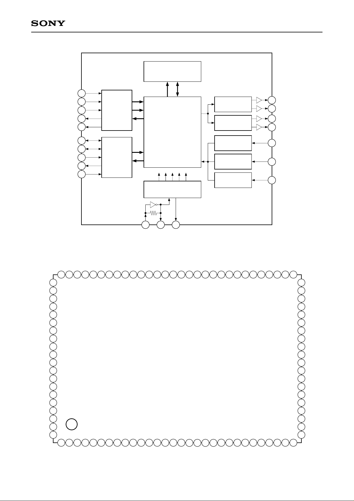
Block Diagram
RVDT
SCK
XLAT
REDY
TRDT
LRCK
BCK
SO
XWO
CXD2720Q
128K bit DELAY RAM
3
AO1P
4
5
6
7
MICRO
COMPUTER
I/F
DAC1
DAC2
25
26
39
40
AO1N
AO2N
AO2P
DSP
88
87
86
SI
12
SERIAL
DATA
I/F
ADC1
ADC2
29
36
AIN1
AIN2
8
ADC3
22
AIN3
CLOCK GENERATOR
/TIMING CIRCUIT
Pin Configuration
6
SS
NC
V
80
78
79
81
X768
82
BFOT
83
INVI
84
NC
85
NC
86
SI
87
BCK
88
LRCK
89
XMST
90
SS7
V
91
NC
92
NC
93
NC
94
NC
95
NC
96
NC
NC
97
98
NC
99
DD3
V
100
D0
AV
1
2
3
0
0
S
SS
V
AV
NC
77
4
RVDT
NC
76
SCK
NC
5
XLAT
75
6
NC
74
7
REDY
NC
73
8
TRDT
NC
72
9
XWO
33
XTLI XTLO BFOT
2
DD
V
NC
NC
69
71
70
12
10
11
0
1
SS
DD
V
V
XRST
5
SS
V
SO
68
13
32
NC
67
14
XS24
82
NC
66
15
TST0
NC
65
16
TST1
NC
64
17
TST2
NC
63
18
TST3
NC
62
19
TST4
NC
61
20
TST5
NC
2
SS
V
60
21
NC
3
S
AV
59
22
NC
58
23
AIN3
NC
3
D
AV
57
24
NC
4
D
AV
56
25
NC
55
26 27
AO1P
NC
54
AO1N
NC
4
S
AV
53
28
4
SS
V
1
S
AV
52
29
NC
51
30
AIN1
NC
1
D
AV
48
47
45
44
33
50
49
46
43
42
41
40
39
38
37
36
35
34
32
31
NC
NC
NC
NC
NC
NC
NC
DD1
V
SS3
V
S5
AV
AO2P
AO2N
D5
AV
D2
AV
AIN2
S2
AV
SS
XV
XTLI
XTLO
DD
XV
– 2 –
Page 3

Pin Description
CXD2720Q
Pin
No.
1
2
3
4
5
6
7
8
9
10
11
12
13
14
Symbol I/O Description
AVS0
VSS0
RVDT
SCK
XLAT
REDY
TRDT
XWO
XRST
VSS1
VDD0
SO
XS24
TST0
—
DRAM digital GND.
—
Digital GND.
I
Data input for microcomputer interface.
I
Shift clock input for microcomputer interface.
I
Latch input for microcomputer interface.
Transmission enabling signal output for microcomputer interface. Transmission
O
prohibited when Low.
O
Serial data output for microcomputer interface.
I
Window open input for synchronization. Normally High.
I
System reset input. Resets when Low.
—
Digital GND.
—
Digital power supply.
O
1-sampling 2-channel serial data output.
I
Serial data 24-/32-bit slot selection. 24-bit slot when Low. (valid for slave mode)
I
Test pin. Normally set Low.
15
16
17
18
19
20
21
22
23
24
25
26
27
28
29
30
31
TST1
TST2
TST3
TST4
TST5
VSS2
AVS3
AIN3
AVD3
AVD4
AO1P
AO1N
AVS4
AVS1
AIN1
AVD1
XVDD
I
Test pin. Normally set Low.
I
Test pin. Normally set Low.
I
Test pin. Normally set Low.
I
Test pin. Normally set Low.
I
Test pin. Normally set Low.
—
Digital GND.
—
CH3 AD converter GND.
I
CH3 AD converter analog input (for microphone input).
—
CH3 AD converter power supply.
—
CH1 DA converter power supply.
O
CH1 DA converter analog positive phase output.
O
CH1 DA converter analog reversed phase output.
—
CH1 DA converter GND.
—
CH1 AD converter GND.
I
CH1 AD converter analog input.
—
CH1 AD converter power supply.
—
Digital power supply for master clock.
32
33
34
35
XTLO
XTLI
XVSS
AVS2
O
Crystal oscillator circuit output.
I
Crystal oscillator circuit input.
—
Digital GND for master clock.
—
CH2 AD converter GND.
– 3 –
Page 4

CXD2720Q
Pin
No.
36
37
38
39
40
41
42
43
44 to 52
53
54 t o 68
69
70
71 t o 79
80
Symbol I/O Description
AIN2
AVD2
AVD5
AO2N
AO2P
AVS5
VSS3
VDD1
NC
VSS4
NC
VSS5
VDD2
NC
VSS6
I
CH2 AD converter analog input.
—
CH2 AD converter power supply.
—
CH2 DA converter power supply.
O
CH2 DA converter analog reversed phase output.
O
CH2 DA converter analog positive phase output.
—
CH2 DA converter GND.
—
Digital GND.
—
Digital power supply.
Normally open.
—
Digital GND.
Normally open.
—
Digital GND.
—
Digital power supply.
Normally open.
—
Digital GND.
81
82
83
84
85
86
87
88
89
90
91 t o 98
99
100
X768
BFOT
INVI
NC
NC
SI
BCK
LRCK
XMST
VSS7
NC
VDD3
AVD0
I
Test input pin. Normally set Low.
O
Clock, frequency-divider output (384fs).
I
Test pin. Normally set Low.
Normally open.
Normally open.
I
1-sampling 2-channel serial data input.
I/O
Serial bit transmission clock for serial input/output data SI and SO.
I/O
Sampling frequency clock for serial input/output data SI and SO.
I
BCK, LRCK master/slave mode switching input. Master mode when Low.
—
Digital GND.
Normally open.
—
Digital power supply.
—
Digital power supply for DRAM.
– 4 –
Page 5
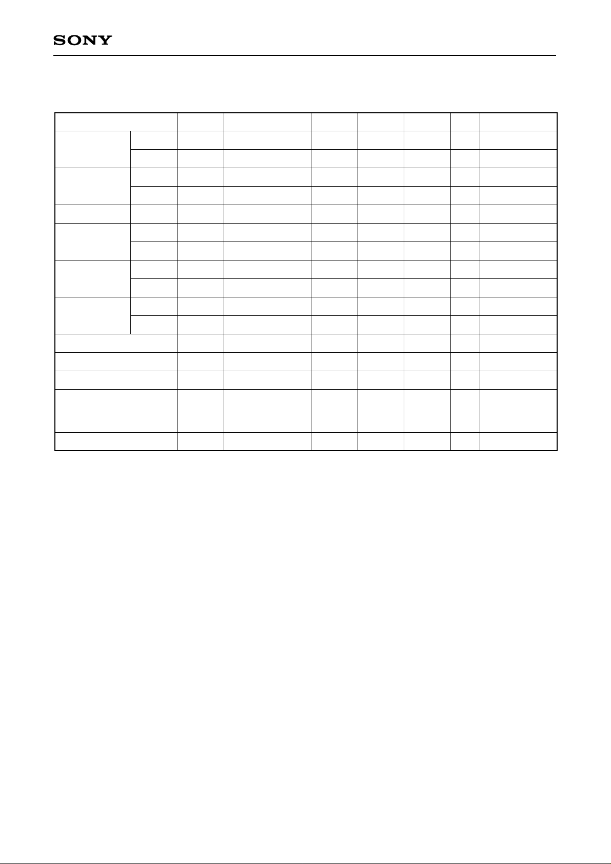
DC Characteristics
(AVD0 to 5 = XVDD = VDD0 to 3 = 5V ± 10%, AVS0 to 5 = XVSS = VSS0 to 7 = 0V, Ta = –20 to +75°C)
Item Symbol Conditions Min. Typ. Max. Unit Applicable pins
High level
Input voltage (1)
Low level
High level
Input voltage (2)
Low level
Input voltage (3)
Output voltage
(1)
Output voltage
(2)
Output voltage
(3)
High level
Low level
High level
Low level
High level
Low level
Input leak current (1)
Input leak current (2)
Output leak current
VIH
VIL
VIH
VIL
VIN
VOH
VOL
VOH
VOL
VOH
VOL
II
II
IOZ
Analog input
IOH = –2.0mA
IOL = 4.0mA
IOH = –6.0mA
IOL = 4.0mA
IOH = –12.0mA
IOL = 12.0mA
VIH = VDD, VSS
VIH = VDD, VSS
VIH = VDD, VSS
0.7VDD
0.8VDD
VSS
VDD – 0.8
VDD – 0.8
VDD/2
–10
–40
–40
0.3VDD
0.2VDD
VDD
0.4
0.4
VDD/2
10
40
40
V
V
V
V
V
V
V
V
V
V
V
µA
µA
µA
CXD2720Q
∗1, ∗4, ∗5
∗1, ∗4, ∗5
∗3
∗3
∗2
∗6, ∗7, ∗8
∗6, ∗7, ∗8, ∗9
∗10
∗10
∗11
∗11
∗1, ∗3, ∗5
∗4
∗8, ∗9
Feedback resistance
Current consumption
∗1
RVDT, SCK, XLAT, XWO, XRST, XS24, TST0 to TST5, X768, SI, XMST
∗2
AIN1, AIN2, AIN3
∗3
INVI
∗4
During input to bidirectional pins BCK, LRCK
∗5
XTLI
∗6
During output from bidirectional pins BCK, LRCK
∗7
SO, BFOT
∗8
TRDT
∗9
REDY
∗10
AO1P, AO1N, AO2N, AO2P
∗11
XTLO
RFB
IDD
fs = 44.1kHz
250k
1M
79
2.5M
90
Ω
mA
Resistance
between
∗5
and ∗11.
– 5 –
Page 6

AC Characteristics
(AVD0 to 5 = XVDD = VDD0 to 3 = 5V±10%, AVS0 to 5 = XVSS = VSS0 to 7 = 0V, Ta = –20 to +75°C)
Serial Audio Interface Timing
[Slave mode]
CXD2720Q
BCK
SI
SO
LRCK
[Master mode]
BCK
LRCK
SO
Item
tDSSO
0.7VDD
0.3VDD
tHSItSSI
DD
0.7V
0.3VDD
tHLR
tDLR
tDMSO
tSLR
0.7VDD
0.3VDD
Symbol Conditions Min. Max. Unit
SI setup time
SI hold time
SO delay time
LRCK setup time
LRCK hold time
LRCK delay time
SO delay time
tSSI
tHSI
tDSSO
tSLR
tHLR
tDLR
tDMSO
Slave mode
Slave mode
Slave mode, CL = 60pF
Slave mode
Slave mode
Master mode, CL = 120pF
Master mode, CL = 60pF
20
40
20
40
50
50
100
ns
ns
ns
ns
ns
ns
ns
– 6 –
Page 7

Microcomputer Interface Timing
[Write]
• Transmission timing for address section, transmission mode section, data section LSB
CXD2720Q
RVDT
SCK
Address LSB Data LSB Data MSB
tSWL
tSWH tDS tDH
Mode MSB
0.7VDD
0.3VDD
0.7VDD
0.3VDD
tLSDtSLP
XLAT
tLWH
tLWL
0.7VDD
0.3VDD
REDY
• Transmission timing from data section MSB to address section and transmission mode section
RVDT
SCK
XLAT
REDY
Data MSB Address LSB Mode MSB
tSS
tSLD
tSBD tLDR
tBSP
0.7VDD
0.3VDD
0.7VDD
0.3VDD
tRLP
[Read]
0.7VDD
0.3VDD
• Transmission timing for address section and transmission mode section is the same as for write.
RVDT
SCK
XLAT
REDY
TRDT
Mode MSB
tSLP
tLWL tLBD
tRSDP
tLDN tSDD
Data MSBData LSB
Address LSB
tSS
0.7VDD
0.3VDD
0.7VDD
0.3VDD
0.7VDD
0.3VDD
– 7 –
Page 8
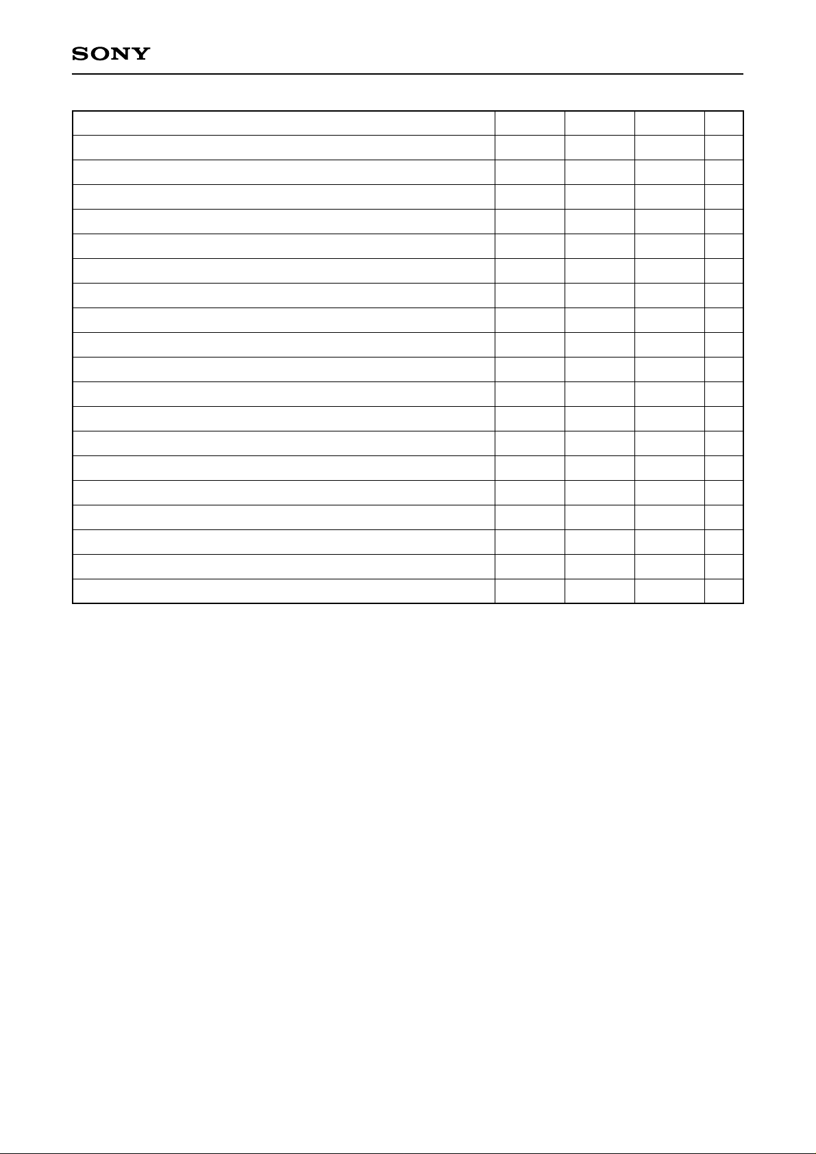
CXD2720Q
Item
RVDT setup time relative to SCK rise
RVDT data hold time from SCK rise
SCK Low level width
SCK High level width
XLAT Low level width
XLAT High level width
SCK rise preceding time relative to XLAT rise
SCK rise wait time relative to XLAT rise
Delay time to REDY fall relative to XLAT rise.
Delay time to REDY fall relative to SCK rise
REDY fall preceding time relative to SCK rise
REDY rise preceding time relative to XLAT rise
REDY rise preceding time relative to SCK fall
XLAT fall wait time relative to SCK rise
XLAT fall delay time relative to REDY fall
Delay time from XLAT rise until TRDT data becomes active
Delay time from SCK rise until TRDT data becomes high-impedance
Delay time from SCK fall until TRDT data is verified
CK rise wait time for next transmission
Symbol Min.
tDS
tDH
tSWL
tSWH
tLWL
tLWH
1t + 20
1t + 20
1t + 20
1t + 20
1t + 20
tSLP
tLSD
3t + 20
tLBD
tSBD
tBSP
tRLP
tRSDP
tSLD
3t + 20
tLDR
tLDN
tSDF
tSDD
tSS
2t + 40
20
20
20
20
20
20
Max.
3t + 50
4t + 50
3t + 80
3t + 80
2t + 70
Unit
ns
ns
ns
ns
ns
ns
ns
ns
ns
ns
ns
ns
ns
ns
ns
ns
ns
ns
ns
Note 1) t is the cycle of 1/2 the clock frequency applied to the XTLI pin. (384fs)
Note 2) REDY and TRDT pins are the values for CL = 60pF.
– 8 –
Page 9

CXD2720Q
Analog Characteristics (AVD0 to 5 = VDD0 to 3 = XVDD = 5.0V, AVS0 to 5 = VSS0 to 7 = XVSS = 0.0V, Ta = 25°C,
DSP: each function = OFF, gain = 1)
[1] ADC + DAC connection total characteristics
The measurement circuit in Figure 1-1 is used. Unless otherwise indicated, the measurement conditions are as
given below.
• Input signal ...1.0Vrms, 1kHz
• fs....................44.1kHz
• Rin.................0Ω
S/N ratio
Item
1.0Vrms, EIAJ (with “A” weighting filter)
1.0Vrms, EIAJ
Measurement conditions Min. Typ. Max.
80 88
0.016
0.03
THD + N
Dynamic range
Channel separation
Level difference between
channels
0.5Vrms, EIAJ
EIAJ
Only ADC characteristics using DAC1,
EIAJ
Only ADC characteristics using DAC1
Rin = 0Ω
0.012
92
108
0.05
1.26
Analog full-scale input level
Rin = 22kΩ
ADC input impedance
Analog current consumption
∗1
Analog input level which outputs digital full scale.
2.06
34.6
21
An optional analog input signal level Vin (Vrms) of 1.26Vrms or more can be set in digital full scale by the
measurement circuit external resistor Rin.
The calculation formula for external resistor Rin is:
Unit
dB
%
dB
dB
dB
Vrms
kΩ
mA
Rin = 27.5 × Vin – 34.6 [kΩ]......(1)
However, THD + N characteristics deteriorate for full-scale output as shown in Graph 1, so use of up to 80%
(when Rin = 0Ω, 0.8 × 1.26 (Vrms) = 1.0 (Vrms) →“analog full scale”) of the analog signal level is recommended
for digital full-scale output.
In this case, the Rin calculation formula is the same as formula (1), except that Vin becomes 1.25 × Vin.
Note that this change causes the output level after ADC + DAC to change.
Most of the above specifications are measurement values for analog full scale.
– 9 –
Page 10
CXD2720Q
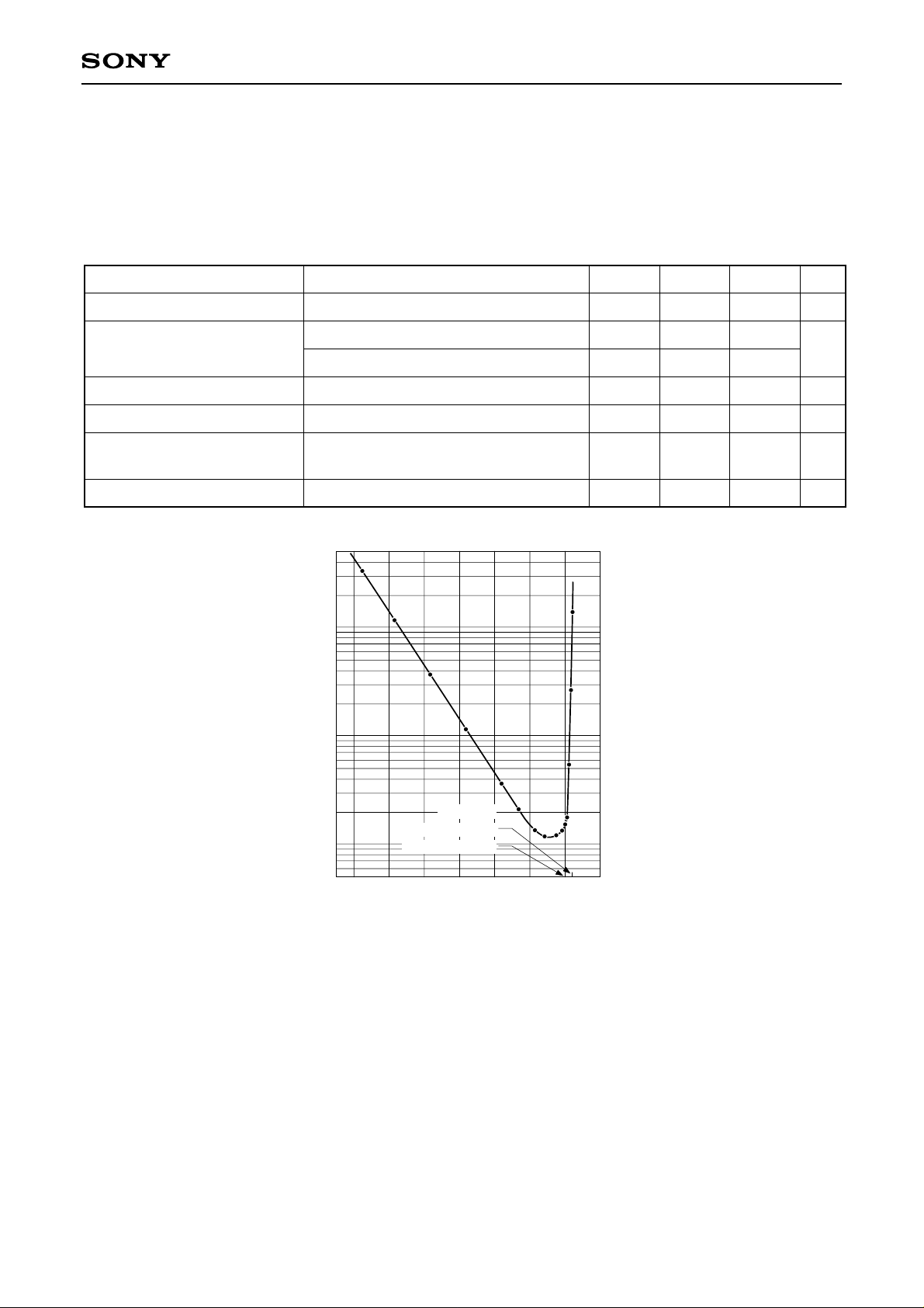
[2] DAC unit characteristics
Use the measurement circuit in Figure 1-2. Unless otherwise specified, the measurement conditions are as
follows.
• Input signal....0dB, 1kHz, 16 bit
• fs....................44.1kHz
Item
S/N ratio
THD + N
Dynamic range
Channel separation
Level difference between
channels
Output level
Measurement conditions Min. Typ. Max. Unit
EIAJ (with “A” weighting filter)
EIAJ (0dB)
EIAJ (–1dB)
EIAJ (–60dB)
EIAJ
EIAJ
EIAJ (Measure at OUT in Figure 1-2.)
1.00
98
0.006
0.004
98
120
0.05
2.0
dB
%
dB
dB
dB
Vrms
0.10
THD + N [%]
0.01
–60
(Rin = 0Ω)
Digital full scale
Analog full scale
–50 –40 –30 –20 –10 0 10
(1Vrms)
Analog input level [dBV]
Graph 1.
– 10 –
Page 11

CXD2720Q
(Master mode)
CXD2720Q
150p
Vin
10µ
Rin
1M
AINx AOxN
22k12k
330p
AOxP
22k12k
39k
39k
150p
Figure 1-1. ADC + DAC Measurement Circuit Diagram
CXD2720Q
(Slave mode)
8200p
2.2k2.2k
820p
OUT
768fs
48fs
fs
DATA
(fs = 44.1kHz)
XTLI
BCK
LRCK AOxN
AOxP
SI
22k12k
330p
22k12k
39k
150p
150p
39k
8200p
Figure 1-2. DAC Measurement Circuit Diagram
2.2k2.2k
820p
OUT
– 11 –
Page 12
CXD2720Q
Description of Functions
1. Master/Slave Modes
[Relevant pins] XMST, LRCK, BCK
When connecting multiple CXD2720Qs, or when using as a pair with a D/A converter such as the CXD2558M,
one of the CXD2720Q should be in master mode to supply LRCK and BCK.
The clock applied to LRCK and BCK in slave mode must be synchronized to either the crystal oscillator clock
of the XTLI and XTLO pins or the external clock input from the XTLI pin
XMST
H
L
Mode LRCK, BCK I/O
Slave mode
Master mode
Input
Output
Table 1-1. LRCK, BCK Mode Setting
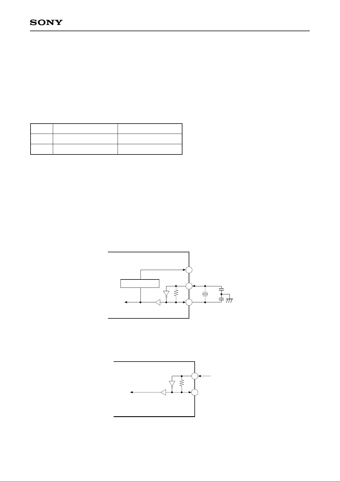
2. Master Clock System
[Relevant pins] XTLI, XTLO, BFOT
768fs (fs = 44.1kHz) is assumed for the master clock system, and the connection is as shown below. (Please
inquire with regard to use at other than fs = 44.1kHz.)
(1) Master
O
384fs
BFOT
Frequency divider
768fs
I
O
XTLI
768fs
XTLO
(2) Slave
768fs
– 12 –
I
O
768fs
XTLI
OPEN
XTLO
Page 13

CXD2720Q
3. Input/Output Synchronization Circuit
[Relevant pins] LRCK, XWO
During normal operation, synchronization is performed automatically to input LRCK (in slave mode), and phase
is matched with serial input data, but if there is a lot of jitter on LRCK, or during power input, synchronization
may be impossible. In this case, forced synchronization can be done by making the XWO pin Low for 2/Fs or
more. Forced synchronization operation is done by the timing of the second LRCK rising edge after the XWO
pin is made Low. When synchronization is completed, return the XWO pin to High.
4. Reset Circuit
[Relevant pins] XRST, XTLI, XTLO
This LSI must be reset after power is turned ON.
Reset is done by making the XRST pin Low for 1/Fs or more after supply voltage satisfies the recommended
operating condition, and the crystal oscillator clock of the XTLI, XTLO pins or the external clock input from the
XTLI pin is correctly applied.
5. Serial Audio Interface (SIF)
[Relevant pins] SI, SO, BCK, LRCK, XS24, XMST
Serial data is used for the external communication of the digital audio data.
The CXD2720Q has one system each for input and output, and each one inputs/outputs 2 channels of data at
1 sampling cycles. Either the 32-bit clock mode or 24-bit clock mode can be selected. In master mode, the 32
bit clock mode is fixed.
(1) Pin Configuration
The pins shown in the table below are assigned to SIF.
Pin
name
SI
SO
BCK
LRCK
XS24
I/O
I
Serial input; taken synchronized to BCK.
O
Serial output; output synchronized to BCK.
BCK input/output; either 32-bit clock mode (64fs) or 24-bit clock mode (48fs). BCK output
I/O
supports 32-bit clock mode only.
I/O
LRCK input/output (1fs).
SI0 slot number (24/32) selection input. Low: 24-bit slot; High: 32-bit slot. Valid only in slave
I
mode. Set High in master mode.
Function
XMST
I
BCK, LRCK master mode/slave mode switching input. Low: master mode; High: slave mode.
Table 5-1. Pin Configuration
– 13 –
Page 14
CXD2720Q
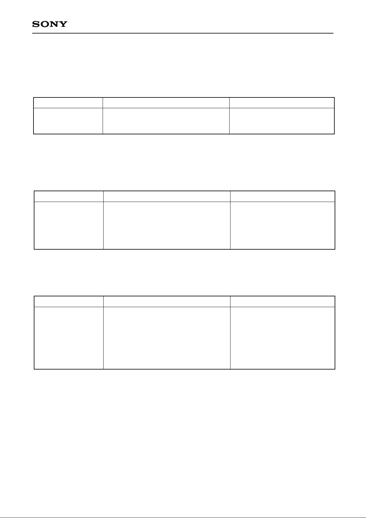
(2) Operation Modes
The LRCK/BCK mode and SI/SO system settings can be selected by the setup register settings as follows.
LRCK/BCK Mode Setting
Setup register
SQ11
SQ10
SQ09
LRCK format
LRCK polarity selection
BCK polarity selection relative to LRCK edge
SI/O System Register Setting
SI system
Setup register
SQ08
SQ07
SQ06
SQ05
SI data list
SI frontward/rearward truncation
SI data word length
SI data word length
Function Contents
“0” : normal, “1” : IIS
“0” : Lch “H”, “1” : Lch “L”
“0” : edge↓, “1” : edge↑
Table 5-2. LRCK/BCK Mode Setting
Function Contents
“0” : MSB first, “1” : LSB first
“0” : Forward truncation,
“1” : Rearward truncation
SQ06 SQ05
0 0 : 16 bit
1 1 : 24 bit
Table 5-3. SI System Register Setting
SO system
Setup register
SQ04
SQ03
SQ02
SQ01
Function Contents
SO data list
SO forward/rearward truncation
SO data word length
Table 5-4. SO System Register Setting
“0” : MSB first, “1” : LSB first
“0” : Forward truncation,
“1” : Rearward truncation
SQ02 SQ01
0 0 : 16 bit
0 1 : 18 bit
1 0 : 20 bit
1 1 : 24 bit
– 14 –
Page 15
CXD2720Q
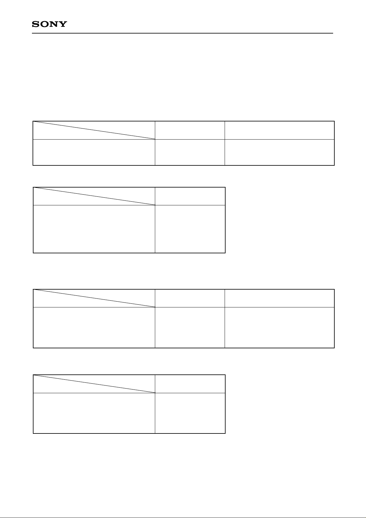
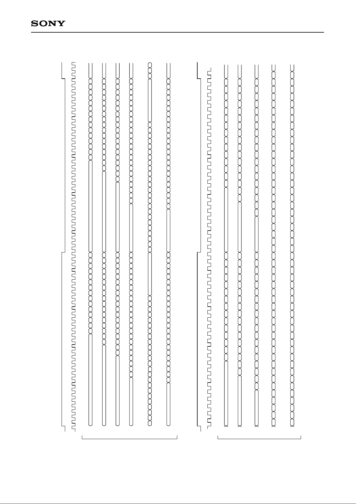
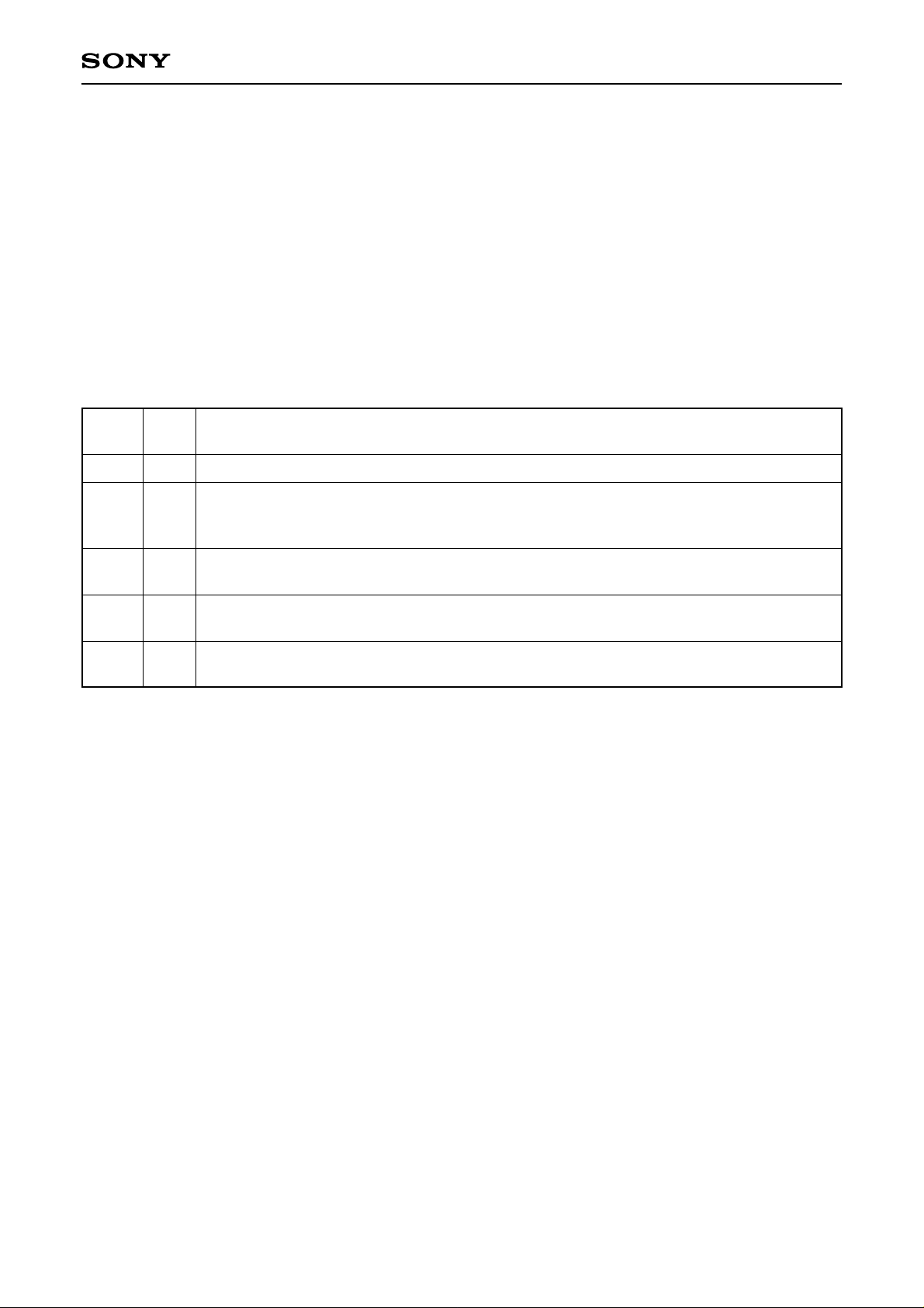
(3) SIF Format
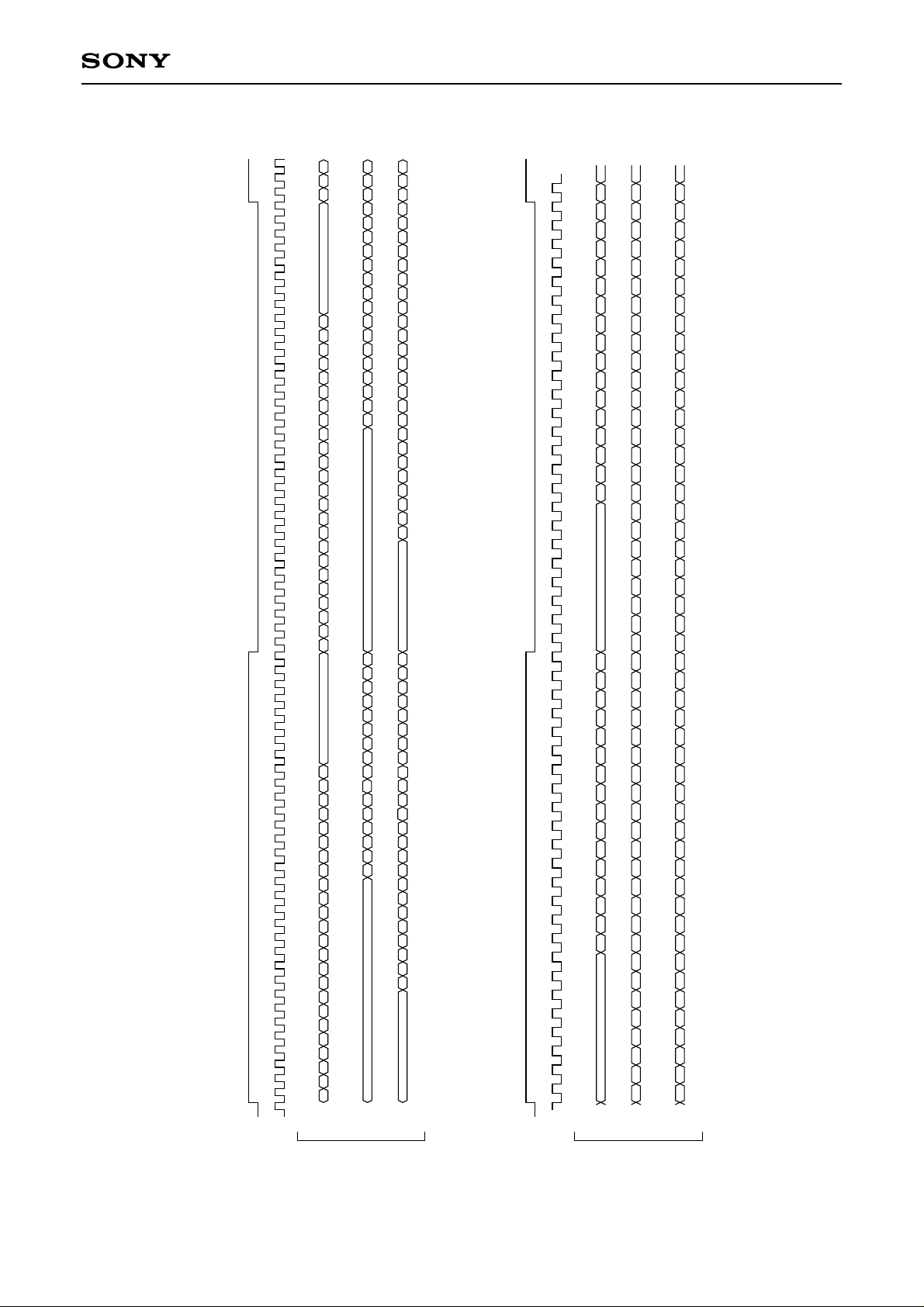
Serial I/F have one input/output system each, and except for slot number, the following formats can be set for
input and output, independently, by setting the setup register. It can also be made to support IIS format, to
enable connection to Philips and other devices. The timing charts for each data format are given on the
following pages.
32-bit slot (XS24 = High)
SI format
MSB first 24 bit Forward truncation
MSB first 16 bit Forward truncation
LSB first 24 bit Rearward truncation
SI format
MSB first 16 bit Rearward truncation
MSB first 18 bit Rearward truncation
MSB first 20 bit Rearward truncation
MSB first 24 bit Rearward truncation
MSB first 24 bit Forward truncation
LSB first 24 bit Rearward truncation
Table 5-6. 32-bit Slot Serial OUT
24-bit slot (XS24 = Low)
SI format
Setup register
Setup register
Setup register
SQ05 SQ06 SQ07
1
1
0
0
1
1
Table 5-5. 32-bit Slot Serial IN
SQ01 SQ02 SQ03
0
0
1
0
0
1
1
1
1
1
1
1
SQ05 SQ06 SQ07
0
1
1
1
1
1
1
0
1
SQ08
0
0
1
SQ04
0
0
0
0
0
1
SQ08
Supplement
Supports 20, 16 bits
Supports 20, 16 bits
Supplement
MSB first 16 bit Rearward truncation
MSB first 24 bit
LSB first 24 bit
Table 5-7. 24-bit Slot Serial IN
SI format
MSB first 16 bit Rearward truncation
MSB first 18 bit Rearward truncation
MSB first 20 bit Rearward truncation
MSB first 24 bit
LSB first 24 bit
Table 5-8. 24-bit Slot Serial OUT
Note 1) When performing 20-bit and 16-bit data input in serial IN 24-bit data format, fill the lower 4 and 8 bits
with “0”, respectively.
Note 2) ∗ means “don't care”.
Setup register
0
0
1
1
1
∗
1
1
∗
SQ01 SQ02 SQ03
0
0
1
1
0
1
0
1
1
1
1
∗
1
1
∗
– 15 –
0
0
1
SQ04
0
0
0
0
1
Supports 20, 16 bits for forward
truncation
Supports 20, 16 bits for rearward
truncation
Page 16
Rch
Invalid
LSBMSB
CXD2720Q
LSBMSB
MSBLSB
15 14 13 12 11 10 09 08 07 06 05 04 03 02 01 00
Rch
Lch
23 22 21 20 19 18 17 16 15 14 13 12 11 10 09 08 07 06 05 04 03 02 01 00
Invalid
13 12 11 10 09 08 07 06 05 04 03 02 01 00
LSBMSB
Invalid
15 14 13 12 11 10 09 08 07 06 05 04 03 02 01 00
LSBMSB
00 01 02 03 04 05 06 07 08 09 10 11 12 13 14 15 16 17 18 19 20 21 22 23
Invalid
MSBLSB
Lch
Invalid
15 14 13 12 11 10 09 08 07 06 05 04 03 02 01 00 15 14 13 12 11 10 09 08 07 06 05 04 03 02 01 00
LSB LSB
Figure 5-1.
MSB MSB
00 01 02 03 04 05 06 07 08 09 10 11 12 13 14 15 16 17 18 19 20 21 22 23
Invalid
Invalid
• LSB first 24 bits rearward truncation
SI
24 bit slot
LRCK
Invalid
23 22 21 20 19 18 17 16 15 14 13 12 11 10 09 08 07 06 05 04 03 02 01 00 23 22 21 20 19 18 17 16 15 14 13 12 11 10 09 08 07 06 05 04 03 02 01 00
MSB LSB MSB LSB
• MSB first 16 bits rearward truncation
• MSB first 24 bits
BCK
SI
LRCK
32 bit slot
15 14
23 22 21 20 19 18 17 16
• MSB first 16 bits rearward truncation
• MSB first 24 bits forward truncation
BCK
Digital Audio Data Input Timing (with polarities: SQ11 = 0, SQ10 = 0, SQ09 = 0)
– 16 –
01 02 03 04 05 06 07 08 09 10 11 12 13 14 15 16 17 18 19 20 21 22 23 00 01 02 03 04 05 06 07 08 09 10 11 12 13 14 15 16 17 18 19 20 21 22 23
00
LSB MSB LSB MSB
• LSB first 24 bits
Page 17
CXD2720Q
Rch
LSBMSB
06
LSBMSB
" 0 " truncation
06
MSBLSB
LSBMSB
14 13 12 11 10 09 08 07 05 04 03 02 01 00
Rch
16 15 14 13 12 11 10 09 08 07 06 05 04 03 02 01 00
18 17 16 15 14 13 12 11 10 09 08 07 05 04 03 02 01 00
15
17
22 21 20 19 18 17 16 15 14 13 12 11 10 09 08 07 06 05 04 03 02 01 00
00 01 02 03 04 05 06 07 08 09 10 11 12 13 14 15 16 17 18 19 20 21 22 23
19
23
" 0 " truncation
14 13 12 11 10 09 08 07 06 05 04 03 02 01 00
MSB
16 15 14 13 12 11 10 09 08 07 06 05 04 03 02 01 00
18 17 16 15 14 13 12 11 10 09 08 07 06 05 04 03 02 01 00
15
17
19
Lch
LRCK
32 bit slot
LSBMSB
LSBMSB LSBMSB
14 13 12 11 10 09 08 07 06 05 04 03 02 01 00
16 15 14 13 12 11 10 09 08 07 06 05 04 03 02 01 00
18 17 16 15 14 13 12 11 10 09 08 07 06 05 04 03 02 01 00
LSB
LSBMSB LSBMSB
MSB
15
17
• MSB first 16 bits rearward truncation
• MSB first 20 bits rearward truncation
• MSB first 18 bits rearward truncation
BCK
22 21 20 19 18 17 16 15 14 13 12 11 10 09 08 07 06 05 04 03 02 01 00
19
23
• MSB first 24 bits rearward truncation
SO
MSBLSB
" 0 " truncation
LSBMSB
Lch
00 01 02 03 04 05 06 07 08 09 10 11 12 13 14 15 16 17 18 19 20 21 22 23
" 0 " truncation
23 22 21 20 19 18 17 16 15 14 13 12 11 10 09 08 07 06 05 04 03 02 01 00 23 22 21 20 19 18 17 16 15 14 13 12 11 10 09 08 07 06 05 04 03 02 01 00
• MSB first 24 bits forward truncation
• LSB first 24 bits rearward truncation
BCK
LRCK
24 bit slot
LSB LSB
14 13 12 11 10 09 08 07 06 05 04 03 02 01 00
MSB
16 15 14 13 12 11 10 09 08 07 06 05 04 03 02 01 00
MSB LSB MSB LSB
15
• MSB first 16 bits rearward truncation
• MSB first 18 bits rearward truncation
18 17 16 15 14 13 12 11 10 09 08 07 06 05 04 03 02 01 00
17
MSB LSB MSB LSB
19
23 22 21 20 19 18 17 16 15 14 13 12 11 10 09 08 07 06 05 04 03 02 01 00 23 22 21 20 19 18 17 16 15 14 13 12 11 10 09 08 07 06 05 04 03 02 01 00
• MSB first 20 bits rearward truncation
• MSB first 24 bits
00 01 02 03 04 05 06 07 08 09 10 11 12 13 14 15 16 17 18 19 20 21 22 23 00 01 02 03 04 05 06 07 08 09 10 11 12 13 14 15 16 17 18 19 20 21 22 23
MSB LSB MSB LSB
• LSB first 24 bits
SO
Figure 5-2.
LSB MSB LSB MSB
Digital Audio Data Output Timing (with polarities: SQ11 = 0, SQ10 = 0, SQ09 = 0)
– 17 –
Page 18
CXD2720Q
6. Microcomputer Interface
[Relevant pins] RVDT, TRDT, SCK, XLAT, REDY
The CXD2720Q performs serial audio interface format setting, volume, coefficient settings of microphone echo
delay amount and others by serial data from the microcomputer.
Further, bidirectional communication such as internal data read from the CXD2720Q to the microcomputer can
be done at the rate of once in 1 LRCK.
(1) Pin Structure
The five external pins indicated in the table below are allocated for microcomputer interface.
Microcomputer interface begins operation when XLAT is received, so RVDT, TRDT, SCK and REDY are
connected in common, and by controlling (wiring) only XLAT separately, multiple CXD2720Qs can be used.
Pin
name
RVDT
TRDT
SCK
XLAT
REDY
I/O
I
Serial data input from microcomputer.
Function
Serial data output to microcomputer. High impedance state unless this pin is set to internal
O
data read state by the microcomputer. Therefore, it is preferable to perform pull-up or pulldown so that potential is not unstable when this pin is not active.
Shift clock for serial data. Input data from RVDT is taken according to SCK rise, and output
I
data from TRDT is sent out according to SCK fall.
Interprets the 8 bits of RVDT before this signal rises as transmission mode data, and the
I
bits before that as address data.
Transmission prohibited while at Low level. Transmission enabled at High. This pin is an
O
open drain, and must be pulled up externally.
Table 6-1. Microcomputer Interface External Pins
– 18 –
Page 19
CXD2720Q
(2) Description of Communication Formats
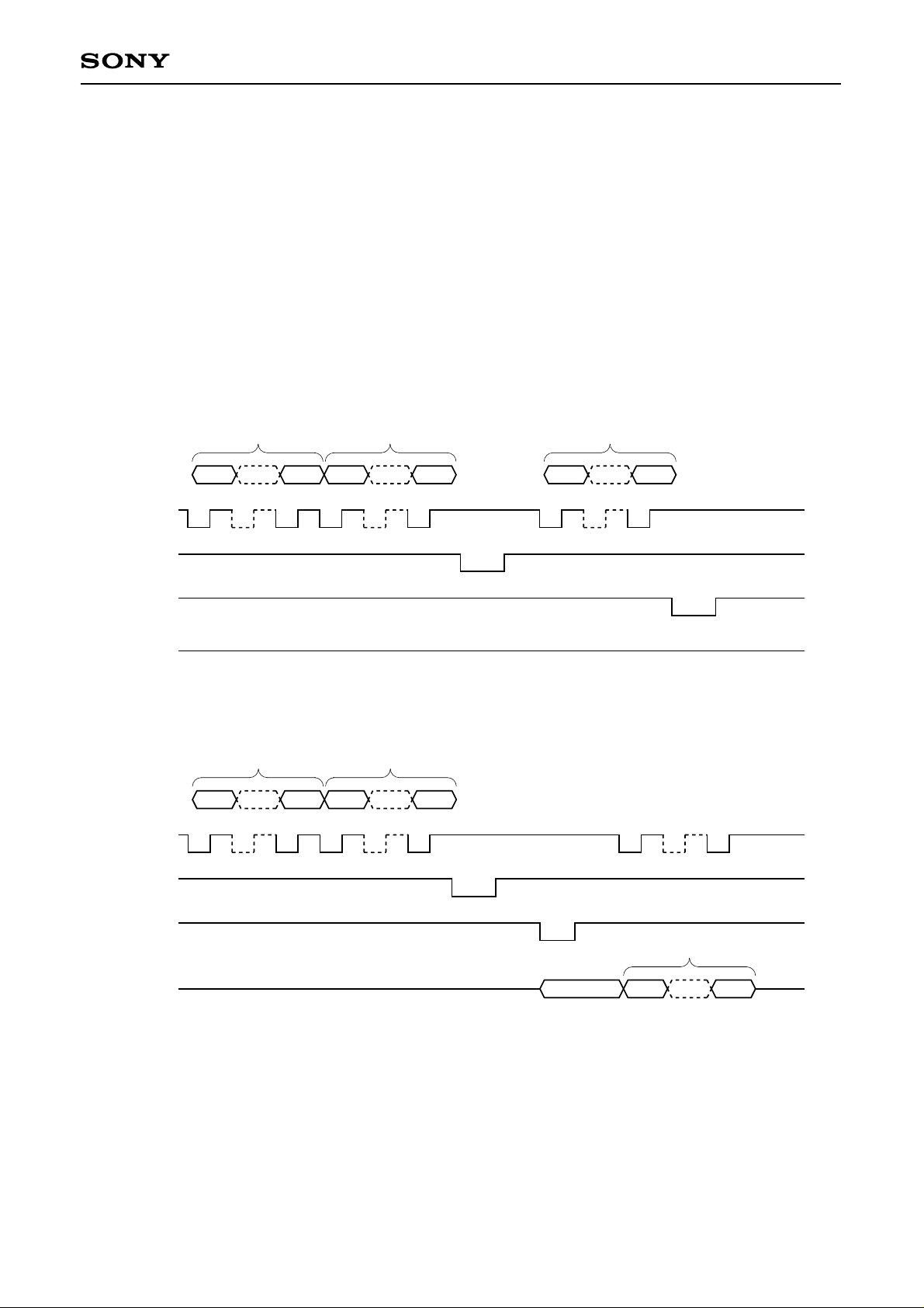
The data transmission timing between the microcomputer interface and coefficient RAM and setup register is
called the SV cycle, and is generated once in 1LRCK.
The SV cycle is generated immediately preceding the signal processing program, so it has absolutely no effect
on signal processing, and there is no risk of the sound being cut.
In read/write modes,
Address section + Mode section + Data section
act as one package of data to perform data transmission between the microcomputer and the CXD2720Q.
[Write] • For coefficient RAM
Address section (8 bits) Mode section (8 bits)
A0 A7 M0 M7 D0 D15RVDT
SCK
XLAT
REDY
TRDT
[Read] • For coefficient RAM
Address section (8 bits) Mode section (8 bits)
RVDT
SCK
A0 A7 M0 M7
Data section (16 bits)
XLAT
REDY
TRDT
Note) For both read and write, the data section is 24 bits for the setup register.
Figure 6-1. Examples of Communication
– 19 –
Data section (16 bits)
D0 D15
Page 20
CXD2720Q
(3) Data Structure
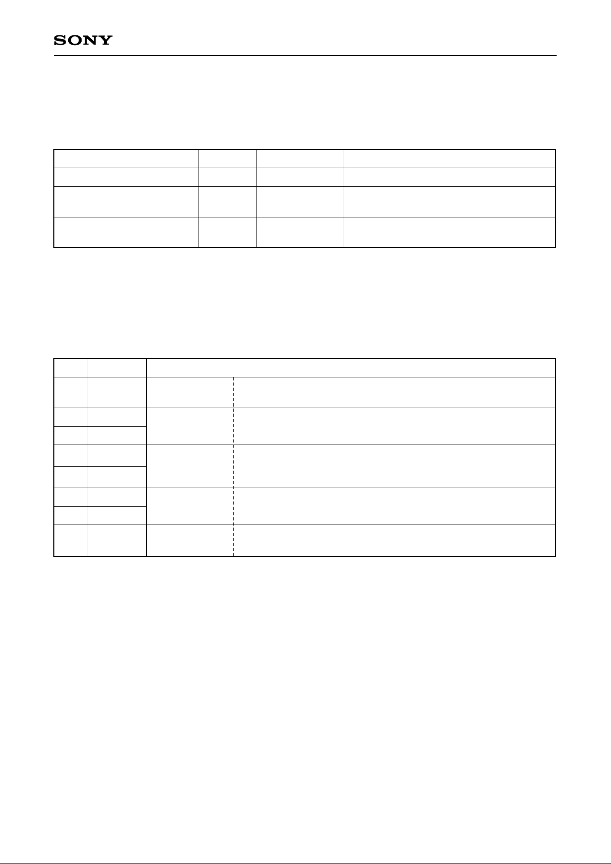
Data structure is classified in three types, as shown in the table below. All data communication is done with
LSB first.
Name
A0 to A7
M0 to M7
D0 to D15/SQ00 to SQ23
Bit length Contents Remarks
8
8
16/24
Address section
Transmission
mode section
Data section
Coefficient RAM is 16 bits; setup register is
24 bits
Table 6-2. Data Structure
(3)-1. Transmission Mode Section
The transmission mode section is 8 bits and has the following functions.
Bit
M7
Name Function
XVMT
SO Mute
0: ON (No sound)
1: OFF
M6
Reserve
M5
M4
M3
VS1
Data type
VS0
VS1 VS0
0 0 Setup register
1 0 Coefficient RAM (K-RAM)
M2
Reserve
M1
M0
VRD
Send/Receive
0: Receive
1: Send
Note) Polarity as seen from the CXD2720Q
Table 6-3. Transmission Mode Section
(3)-2. Address Section
The coefficient RAM has a 192-word structure, so the address section is 8 bits. The setup register has a 1word structure, so the address section data may be optional.
(3)-3. Data Section
Sixteen SCK are required, as the coefficient RAM has a 16-bit structure (D0 to D15). The setup register has a
24-bit structure (SQ00 to SQ23), so twenty-four SCK are required.
– 20 –
Page 21
CXD2720Q
(4) Details of Communication Methods
The definitions of signal timing required for control from the microcomputer are given below.
(4)-1. Write
First, address section data and mode section data are sent from the microcomputer, synchronized to SCK, to
the RVDT pin.
The address section data is 8 bits both for the coefficient RAM and setup register, and the setup register
transmits optional data for 1 word length. Address section data is sent with LSB first.
Mode section data is fixed at 8 bits regardless of content.
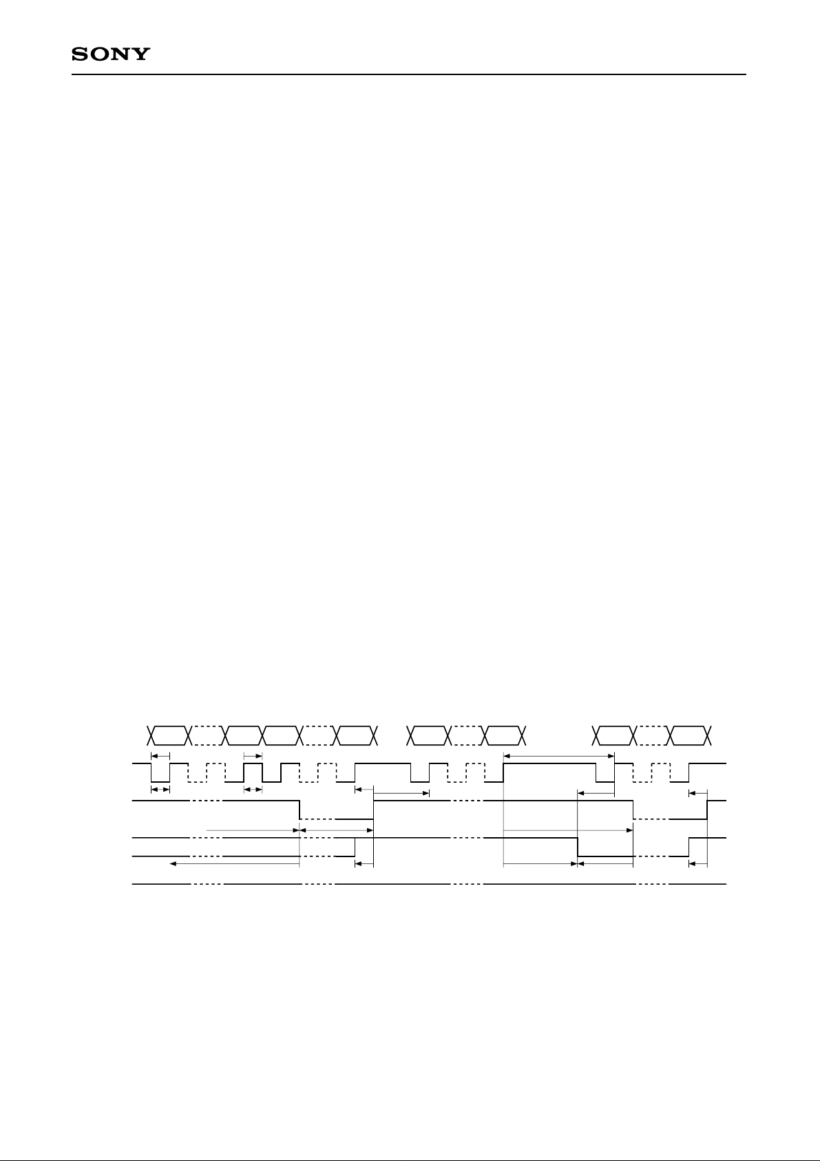
The phase relationship between SCK and RV data (data applied to the RVDT pin) has the following restrictions:
• RV data must be verified before SCK rise (tDS ≥ 20ns).
• RV data must be held for 1t + 20ns or more after SCK rise (tDH).
SCK itself has the following restrictions:
• SCK Low level must be 1t+ 20ns or more (tSWL).
• SCK High level must also be 1t + 20ns or more (tSWH).
After raising SCK which corresponds to mode section final data, XLAT is raised (tSLP ≥ 20ns). XLAT Low level
width must be maintained at 1t + 20ns or more (tLWL). Further, fall timing restrictions are:
• for the preceding transmission, if REDY falls due to SCK, as for write, 3t + 20ns or more is required. (tSLD)
• for the preceding transmission, if REDY falls due to XLAT, as for read, 20ns or more is required. (tLDR)
Further, if preceding transmissions have been performed and REDY = Low, it is necessary to wait for REDY =
High to raise XLAT.
The procedure until this point is the same for write and read.
D0/SQ00 D15/SQ23
A0RVDT A7 M0 M7 SQ00 SQ23 A0 M7
SCK
XLAT
REDY
TRDT
tDS tDH
tSWL tSWH
tSLD or tLWH
tLDR
High-Z
tSLP
tLWL
tLSD
tSLD
tSBD tLDR tRLPtRLP
tSS
tBSP tSLP
Figure 6-2. Write Timing
– 21 –
Page 22

CXD2720Q
Data section write begins after XLAT rise, and here also transmission must be with LSB first, with tDS and tDH
restrictions. In addition, after raising XLAT at the starting point for sending to the data section, wait for 3t +
20ns or more for the first SCK rise. (tLSD)
When 16 bits (coefficient RAM) or 24 bits (setup register) of this write is repeated, REDY = Low within 4t + 50ns,
and the microcomputer is informed of waiting status for the SV cycle, which is the dedicated data rewrite cycle
by microcomputer interface. (tSBD)
When REDY goes High again, the corresponding data is written.
The next communication restarts by using the REDY signal as follows.
• When REDY = Low, the SCK for the next transmission can rise (tBSP ≥ 20ns ).
• In the same way, when REDY = Low, the XLAT for the next transmission can fall (tLDR ≥ 20ns).
REDY will fall due to this transmission, but it is prohibited for XLAT to rise for the next transmission before the
REDY rises. Be sure to raise the next XLAT after REDY falls (tRLP ≥ 20ns ).
In order to restart the next transmission without using the REDY signal, the following conditions must be observed:
• There should be 2t + 40ns or more left between the SCK rise for the final data section and the SCK rise for
the next transmission (tSS).
• In the same way, the XLAT for the next transmission can fall after waiting 3t + 20ns or more after the final
data section SCK rise (tSLD).
The tss and tSLD here are shorter times than tSBD ≤ 4t + 50ns, so the restriction conditions are not much strict.
However, even in this case the rise of XLAT for the next transmission must come after REDY rise (tRLP ≥
20ns).
Further, the restriction for XLAT fall at the starting point of this write from tSLD can be:
• tSLD ≥ 3t + 20ns if the preceding transmission was “write”.
– 22 –
Page 23

CXD2720Q
(4)-2. Read
First, address section and mode section data are transmitted synchronized to SCK, and XLAT is raised
matched with this; the procedure until this point is the same as for write, so the description is omitted here.
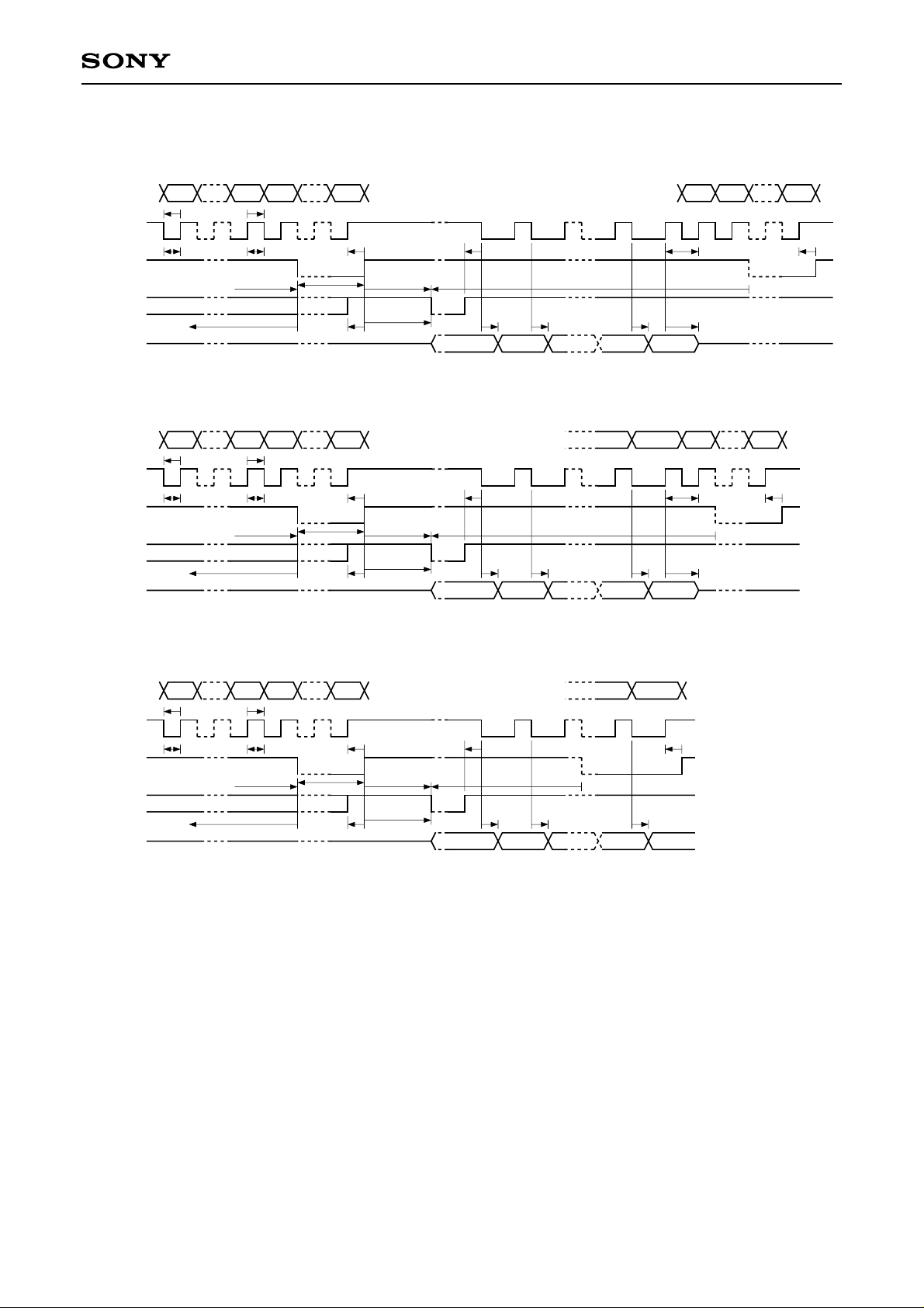
Read differs from write in that after XLAT rise, REDY falls within 3t + 50ns (tLBD), and the microcomputer is
informed of SV cycle waiting.
At this time, the TRDT pin changes from high-impedance state to active state (tLDN ≤ 3t + 80ns) simultaneously
with REDY fall. When the read data is ready, the REDY pin changes from Low to High. When the data read out
from the TRDT pin is made TR, and SCK falls (tRSDP ≥ 20ns) when the REDY pin goes High, the first TR data
is defined within 2t + 70ns (tSDD). The microcomputer reads this data at SCK rise. The TR data is read in order
from the LSB with 16 bits for the coefficient RAM and 24 bits for the setup register by adding SCK, the
corresponding data is all read, and then read is completed.
Next, the method for restarting transmission after read is completed is described.
As in Case 1, there is a method for sending address section and mode section data consecutively after reading
all of the 16- or 24-bit data. There should be 2t + 40ns or more left between the SCK rise for the final data read
and the next SCK rise (tss), and this is established by the conditions tSWL ≥ 1t + 20ns and tSWH ≥ 1t + 20ns.
Further, at this read REDY changes from High to Low, but it is prohibited for the XLAT for the next
transmission to fall before this. If REDY = Low has been verified, XLAT can fall (tLDR ≥ 20 ns).
Also, while 16- or 24-bit data is being read from the TRDT pin, address and mode section data writing to the
RVDT pin for the next transmission can be started.
In Case 3, the final section of read data and the final data in the mode section overlap, and this allows shifting
to the next transmission processing in the shortest possible time after data read.
It is also possible to have data read and address and mode section write overlap partially, as shown by Case 2.
– 23 –
Page 24
CXD2720Q
RVDT
SCK
XLAT
REDY
TRDT
RVDT
SCK
XLAT
REDY
TRDT
A0
tDS tDH
tSWL tSWH tSLP tRSDP tSS tSLP
tSLD or tLWH
tLDR tRLP tSDD tSDD tSDD tSDF
A0
tDS tDH
tSWL tSWH tSLP tRSDP tSS tSLP
tSLD or tLWH
tLDR tRLP tSDD tSDD tSDD tSDF
A7 M0 M7 A1 M7A0
tLWL
A7 M0 M7 A6 M7A5
tLWL
tLBD
t
LDN
case1
tLBD
t
LDN
case2
SQ00 SQ23SQ22
D15/SQ23D0/SQ00 D14/SQ22
SQ00 SQ23SQ22
D15/SQ23D0/SQ00 D14/SQ22
tLDR
tLDR
RVDT
SCK
XLAT
REDY
TRDT
A0
tDS tDH
tSWL tSWH tSLP tRSDP tSLP
tSLD or tLWH
tLDR tRLP tSDD tSDD tSDD
A7 M0 M7 M7
tLWL
tLBD
t
LDN
tLDR
SQ00 SQ23SQ22
case3
Figure 6-3. Read Timing
D15/SQ23D0/SQ00 D14/SQ22
– 24 –
Page 25
CXD2720Q
7. Setup Register
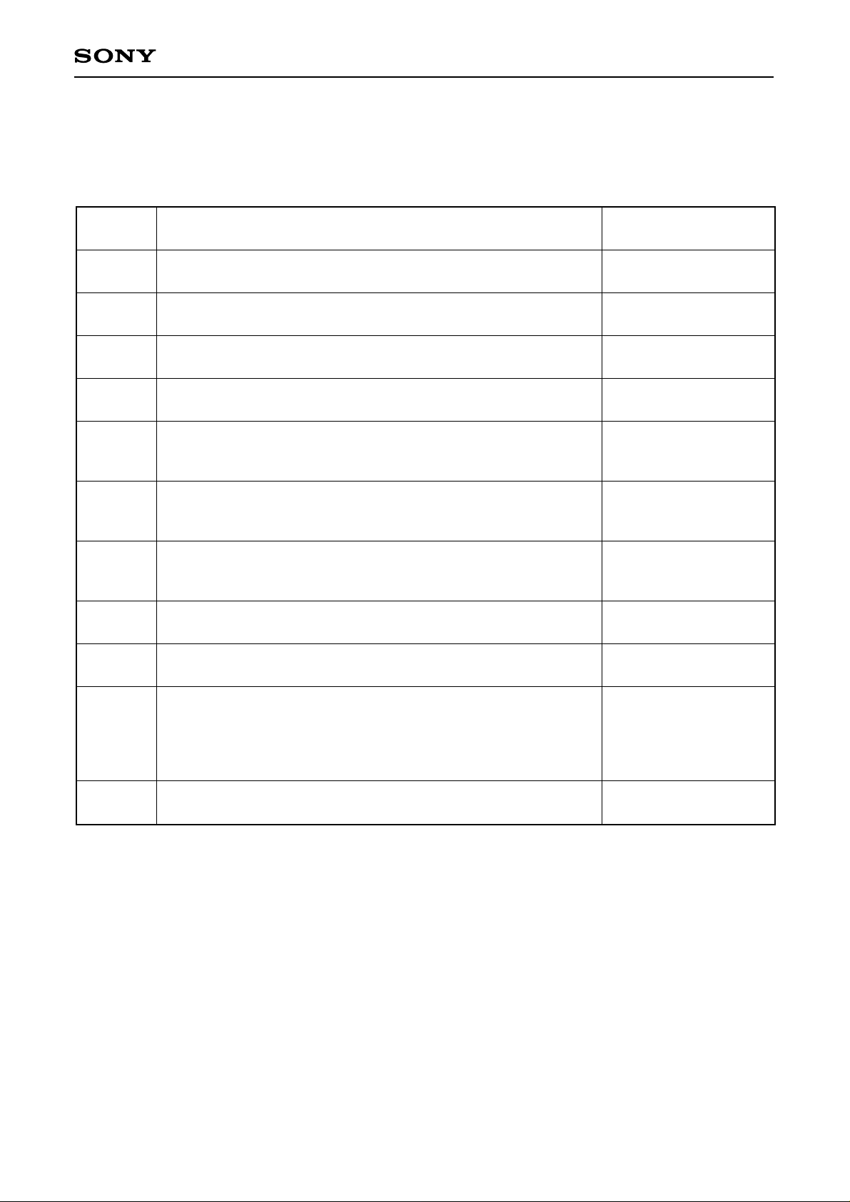
When the setup register is selected for microcomputer interface transmission mode, the following settings are
possible for serial audio interface and DAC.
Data
section bit
SQ23 to 12
SQ11
SQ10
SQ09
SQ08
SQ07
SQ06, 05
SQ04
Reserve bit
LRCK format
LRCK polarity selection
BCK polarity selection
relative to LRCK edge
SI data list
SI frontward/rearward
truncation
SI data word length
SO data list
Control When system reset is Low
Must be Low for setup register setting
change
0: normal
1: IIS
0: Lch High
1: Lch Low
0: Falling edge
1: Rising edge
All Low
Normal
Lch High
Falling edge
0: MSB first
1: LSB first
MSB first
(24-bit rearward truncation)
0: Frontward truncation
(valid only for MSB first/24 bits/32 slots)
Frontward truncation
1: Rearward truncation
SQ06 SQ05
0 0 : 16 bits
16 bits
1 1 : 24 bits
0: MSB first
1: LSB first
LSB first
SQ03
SQ02, 01
SQ00
SO frontward/rearward
truncation
SO data word length
DAC forced mute
0: Frontward truncation
1: Rearward truncation
SQ02 SQ01
0 0 : 16 bits
0 1 : 18 bits
1 0 : 20 bits
1 1 : 24 bits
0: ON
1: OFF
Table 7-1.
Frontward truncation
16 bits
ON
– 25 –
Page 26
CXD2720Q
8. Coefficient RAM Setting
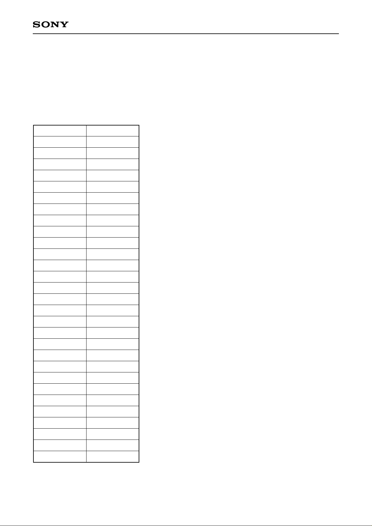
When the coefficient RAM is selected in microcomputer interface transmission mode, the coefficient parameters
such as each section's volumes and microphone echo delay amount can be set. Data settings other than those
given following in Tables 8-1 and 8-2 are “don't care”.
(1) Fixed Values for System Initialization
When the system is initialized, the coefficient RAM must be set at the fixed values, shown below, due to
internal operation.
Address
01H
02H
03H
0DH
12H
13H
14H
15H
16H
17H
19H
1AH
1BH
1DH
20H
21H
Fixed value
68A9H
5121H
0000H
0000H
8B2AH
3BF7H
38DFH
4E77H
2E90H
0000H
0000H
2000H
4000H
4000H
0010H
4000H
23H
24H
25H
26H
27H
28H
2DH
30H
32H
41H
46H
50H
58H
4000H
1600H
2A00H
3FF0H
8000H
0000H
0008H
0000H
0000H
8000H
0000H
0008H
0008H
Table 8-1.
∗
For Fs = 44.1kHz. Please inquire with regard to use at other than Fs = 44.1kHz, as the fixed values change.
– 26 –
Page 27
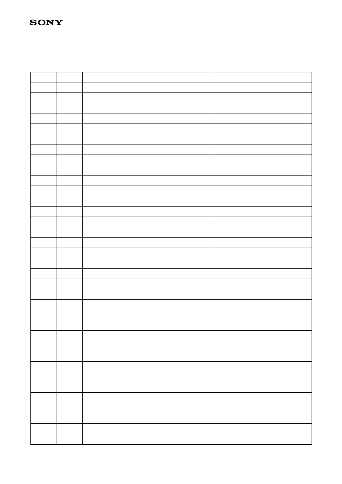
(2) Setting Data
The relationships between the coefficient RAM and each function during DSP operation are as follows.
CXD2720Q
Address
00H
04H
05H
06H
07H
08H
09H
0AH
0BH
0CH
0EH
0FH
10H
11H
18H
22H
Name Function Setting value
Ki
Ke
KisLm
KisRc
KiaLm
KiaRc
KisRm
KisLc
KiaRm
KiaLc
DC1sw
DC1f0
PL
PR
Kvc
nRpR
SI data input level control
De-emphasis ON/OFF
SI CH1 data → Lch mix
SI CH2 data → Lch mix
ADC CH1 data → Lch mix
ADC CH2 data → Lch mix
SI CH2 data → Rch mix
SI CH1 data → Rch mix
ADC CH2 data → Rch mix
ADC CH1 data → Rch mix
DC cut1 ON/OFF for accompaniment
DC cut1 cut-off frequency for accompaniment
Panpot volume for voice cancellation
Panpot volume for voice cancellation
Voice cancelling ON/OFF
Pitch ratio for accompaniment
Refer to Table 12-1 for setting value
ON/AC19H; OFF/0000H
Refer to Table 12-1 for setting value
Refer to Table 12-1 for setting value
Refer to Table 12-1 for setting value
Refer to Table 12-1 for setting value
Refer to Table 12-1 for setting value
Refer to Table 12-1 for setting value
Refer to Table 12-1 for setting value
Refer to Table 12-1 for setting value
ON/4000H; OFF/0000H
Refer to Table 14-1 for setting value
Refer to Table 9-1 for setting value
Refer to Table 9-1 for setting value
ON/8000H; OFF/0000H
Refer to Table 10-1 for setting value
2EH
31H
33H
34H
35H
36H
37H
38H
39H
3AH
3BH
3CH
3DH
3EH
3FH
40H
42H
Ks
Kimc
DC2f0
DC2sw
PEQa
PEQb1
PEQb2
PEQg
HC1a1
HC1a0
HC1b
Kdry
Keff
KLm
KRm
KLo
KRo
Key control ON/OFF for accompaniment
Microphone input level control
DC cut2 cut-off frequency for voice
DC cut2 ON/OFF for voice
PEQ coefficient for voice
PEQ coefficient for voice
PEQ coefficient for voice
PEQ coefficient for voice
High cut1 for voice
High cut1 for voice
High cut1 for voice
Microphone input direct sound mix
Microphone input echo mix
Key control output Lch mix for accompaniment
Key control output Rch mix for accompaniment
System volume Lch
System volume Rch
ON/8000H; OFF/0000H
Refer to Table 12-1 for setting value
Refer to Table 14-1 for setting value
ON/4000H; OFF/0000H
Refer to Table 14-4 for setting value
Refer to Table 14-4 for setting value
Refer to Table 14-4 for setting value
Refer to Table 14-5 for setting value
Refer to Table 14-2 for setting value
Refer to Table 14-2 for setting value
Refer to Table 14-2 for setting value
Refer to Table 12-1 for setting value
Refer to Table 12-1 for setting value
Refer to Table 12-1 for setting value
Refer to Table 12-1 for setting value
Refer to Table 12-1 for setting value
Refer to Table 12-1 for setting value
44H
45H
Tdo
Kre
Microphone echo delay amount
Microphone echo read tap volume
Table 8-2 (1). Coefficient RAM Setting Data (1/2)
– 27 –
Refer to Table 11-1 for setting value
Refer to Table 12-2 for setting value
Page 28

CXD2720Q
Address
47H
49H
4AH
4BH
4CH
4DH
53H
5AH
5BH
Name Function Setting value
Tre
Krd
Kfb
HC2a1
HC2a0
HC2b
VnRpR
Krmc
Krmp
Microphone echo read tap address
Microphone echo input sound mix
Microphone echo reverberation sound mix
Microphone echo high cut2
Microphone echo high cut2
Microphone echo high cut2
Voice pitch ratio
Microphone input mix
Voice pitch control output mix
Refer to Table 11-1 for setting value
Refer to Table 12-1 for setting value
Refer to Table 12-1 for setting value
Refer to Table 14-3 for setting value
Refer to Table 14-3 for setting value
Refer to Table 14-3 for setting value
Refer to Table 10-1 for setting value
Refer to Table 12-1 for setting value
Refer to Table 12-1 for setting value
Table 8-2. Coefficient RAM Setting Data (2/2)
∗
Refer to 13. DSP Signal Flow regarding the names.
9. Voice Canceller Settings
[Relevant pins] PL (address = 10H), PR (address = 11H), Kvc (address = 18H)
The vocal sound set at the center can be cancelled by setting Kvc = 8000H and PL, PR = 7000H.
Voice canceling at other than center setting can be done by the panpot volume.
Panpot volume value is PL for CH1, and PR for CH2, and at the center position they are both 0.857. When
voice cancellation is OFF, set Kvc = 0000H and PL, PR = 0000H.
PL and PR setting values are hexadecimal notation with D15 as MSB and D0 as LSB.
PL
7000H
7000H
7000H
7000H
7000H
7000H
7000H
7000H
PR Setting position PL PR Setting position
7000H
6000H
5000H
4000H
3000H
2000H
1000H
0000H
center
CH2
7000H
6000H
5000H
4000H
3000H
2000H
1000H
0000H
7000H
7000H
7000H
7000H
7000H
7000H
7000H
7000H
center
CH1
Table 9-1. Settings for Voice Canceller Panpot Volume
– 28 –
Page 29

CXD2720Q
10. Key Controller Setting
[Relevant coefficients] nRpR (address = 22H), Ks (address = 2EH), VnRpR (address = 53H),
Krmp (address = 5BH)
(1) Key Controller Pitch Ratio
nRpR (D15,.....,D2) is a 2’s complement format with a decimal point between D14 and D13, and sets the
desired pitch ratio directly. (VnRpR has the same type of setting as nRpR.)
nRpR = ∑Dn × 2
15
n = 2
The expression range for the pitch ratio is: –2.0 ≤ nRpR ≤ 2.0 – 2
n–14
–12
but for practical use it is: –0.5 ≤ nRpR ≤ 1.0
or ±1 octave.
Use within a range of ± half an octave is recommended for quality of sound, although it depends on the aim
and the source.
Also, the algorithm is such that allophones will not be generated even when nRpR setting value is changed.
(2) Notes on Key Controller OFF
The pitch does not change when nRpR and VnRpR are set to 0000H (OFF) when the key controller is OFF,
but depending on the internal state during OFF, there is no guarantee that the input value will be output as is.
During OFF, after setting nRpR and VnRpR to 0000H (OFF), set the pitch control section to through state with
the following settings.
Accompaniment controller OFF: Ks = 0000H (OFF)
Voice key controller OFF: sKrmp = 0000H (OFF)
– 29 –
Page 30
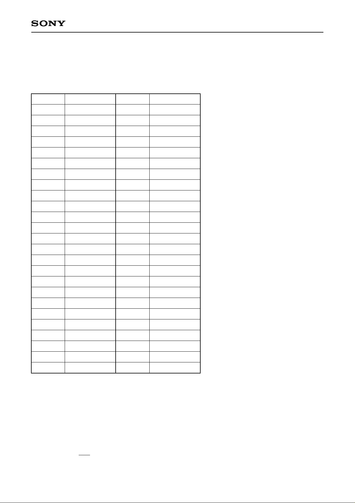
(3) Examples of Key Controller Setting
Examples of pitch ratio setting are illustrated below.
nRpR setting values are hexadecimal notation with D15 as MSB and D2 as LSB for a total of 14 bits.
(D1 and D0 can be optional data.)
CXD2720Q
CENT
0
+50
+100
+150
+200
+250
+300
+350
+400
+450
+500
+550
+600
+650
+700
+750
nPpR CENT nPpR
0000H
01E0H
03CEH
05CAH
07D6H
09F1H
0C1BH
0E56H
10A2H
12FFH
156EH
17EEH
1A82H
1D29H
1FE4H
22B3H
0
–50
–100
–150
–200
–250
–300
–350
–400
–450
–500
–550
–600
–650
–700
–750
0000H
FE2EH
FC69H
FAB1H
F905H
F765H
F5D2H
F44AH
F2CCH
F15AH
EFF3H
EE95H
ED42H
EBF8H
EAB8H
E980H
+800
+850
+900
+950
+1000
+1050
+1100
+1150
+1200
2597H
2892H
2BA2H
2EC9H
3208H
3560H
38D0H
3C5BH
4000H
–800
–850
–900
–950
–1000
–1050
–1100
–1150
–1200
E852H
E72CH
E60EH
E4F9H
E3ECH
E2E6H
E1E8H
E0F1H
E000H
Table 10-1. Pitch Ratio Setting Examples
The numeric representation format for pitch ratio here is:
nRpR = ∑Dn × 2
15
n = 2
The numeric representation range is: –2.0 ≤ nRpR ≤ 2.0 – 2
n–14
–12
Also, the relationship formula with music word cent value C is:
C
nRpR = 2 – 1, C = 1200 log2[nRpR + 1] [cent]
1200
The semitone at average ratio is 100 [cent].
– 30 –
Page 31
CXD2720Q
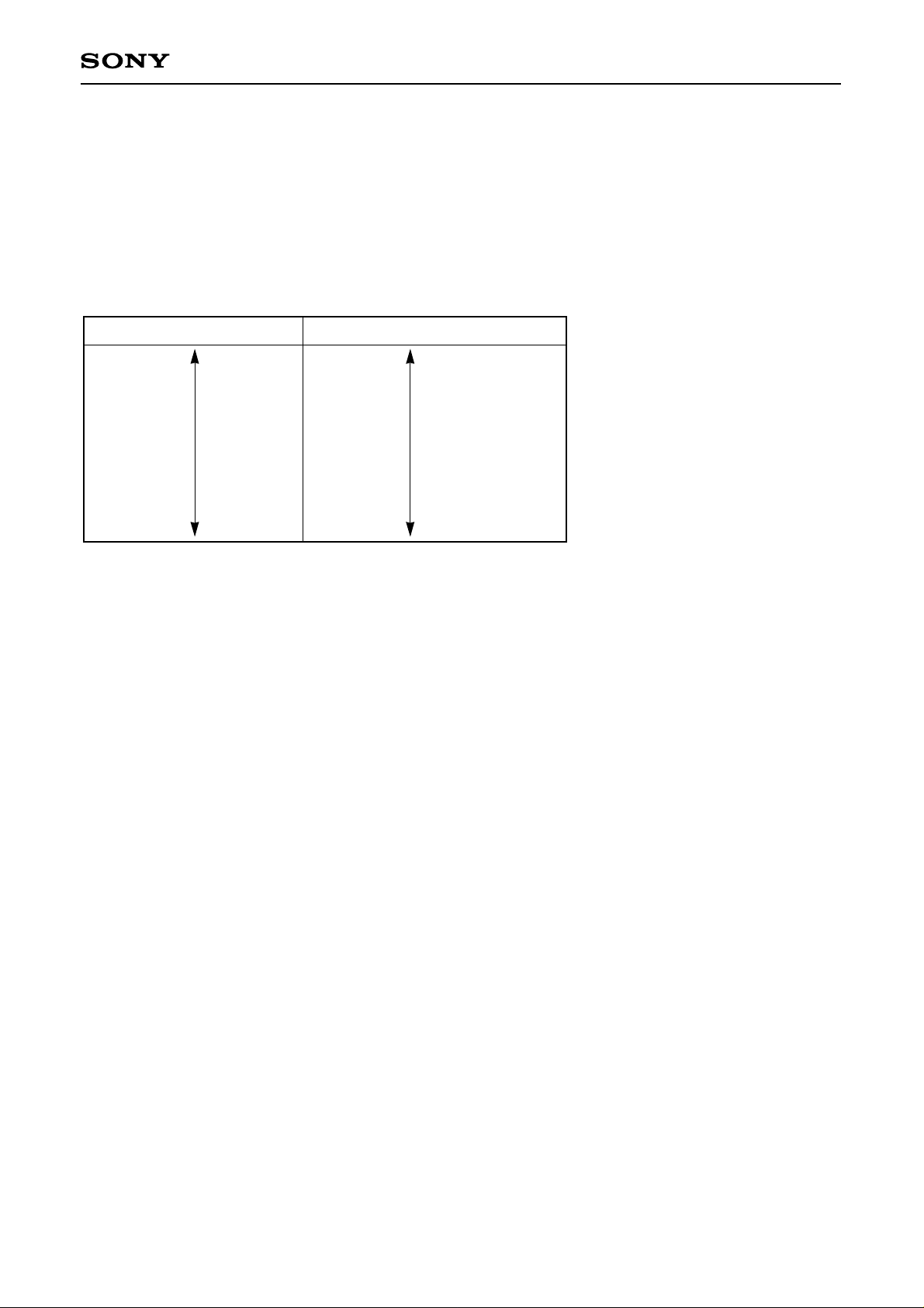
11. Microphone Echo Delay Amount Setting
[Relevant coefficients] Tdo (address = 44H), Tre (address = 47H)
Microphone echo delay amount can be varied by setting coefficient Tdo (12 bits from D14 to D3) values. The
relationships between the coefficient and the delay amount are shown in Table 11-1.
Coefficient Tre (12 bits from D14 to D3) is microphone input echo initial delay time.
Set in the range of 0008H to Tdo.
Setting value Tdo
0008H
0010H
0018H
·
·
·
·
7ff0H
7ff8H
0000H
4096step
Delay (fs = 44.1kHz)
0.045ms
·
·
·
·
·
·
·
·
185.76ms
0.045 ms/step
setting possible
Table 11-1. Microphone Echo Delay Amount Setting
∗
When Fs = 44.1kHz. Please inquire with regard to use at other than Fs = 44.1kHz, as the delay amount changes.
– 31 –
Page 32
CXD2720Q
12. Input/Output Level Settings
[Relevant coefficients] Ki (address = 00H), KisLm (address = 05H), KisRc (address = 06H),
KiaLm (address = 07H), KiaRc (address = 08H), KisRm (address = 09H),
KisLc (address = 0AH), KiaRm (address = 0BH), KiaLc (address = 0CH),
Kimc (address = 31H), Kdry (address = 3CH), Keff (address = 3DH),
KLm (address = 3EH), KRm (address = 3FH), KLo (address = 40H),
KRo (address = 42H), Kre (address = 45H), Krd (address = 49H),
Kfb (address = 4AH), Krmc (address = 5AH), Krmp (address = 5BH)
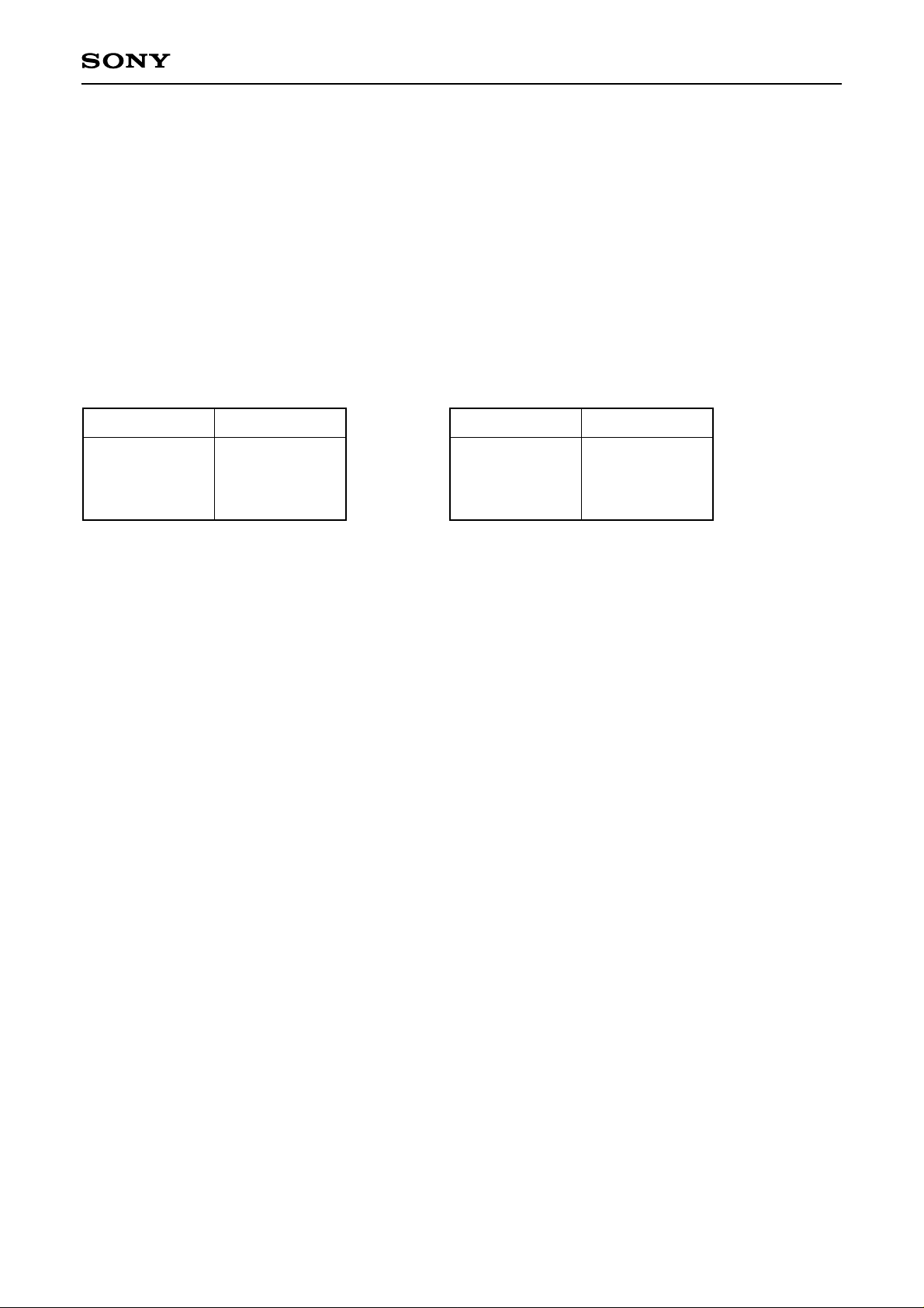
The input/output levels and volumes are 2’s complement format with a decimal point between D15 and D14,
and hexadecimal notation with D15 as MSB and D0 as LSB.
The coefficient and level relationships are as follows.
D15 to D0
8000H
↓
FFFFH
0000H
Table 12-1. Input/Output Level Settings
(other than Kre)
Level D15 to D0
0dB
8000H
↓
–90.31dB
– ∞
FFFFH
0000H
Table 12-2. Input/Output Level Settings
Level
+12.04dB
↓
↓
–78.27dB
– ∞
(Kre)
The input/output levels for 8001H to FFFEH are determined by the following formulas.
14
(Coefficient value) = [ (–1) × D15 + ∑Dn × 2
n = 0
14
(Coefficient value) = [ (–1) × D15 + ∑Dn × 2
n = 0
n–15
] × (–1) for other than Kre
n–15
] × (–4) for Kre
Input/output level = 20 log [coefficient value] dB
∗
D15 to D0 are negative values, but the calculation is (–1) × (D15 to D0).
– 32 –
Page 33
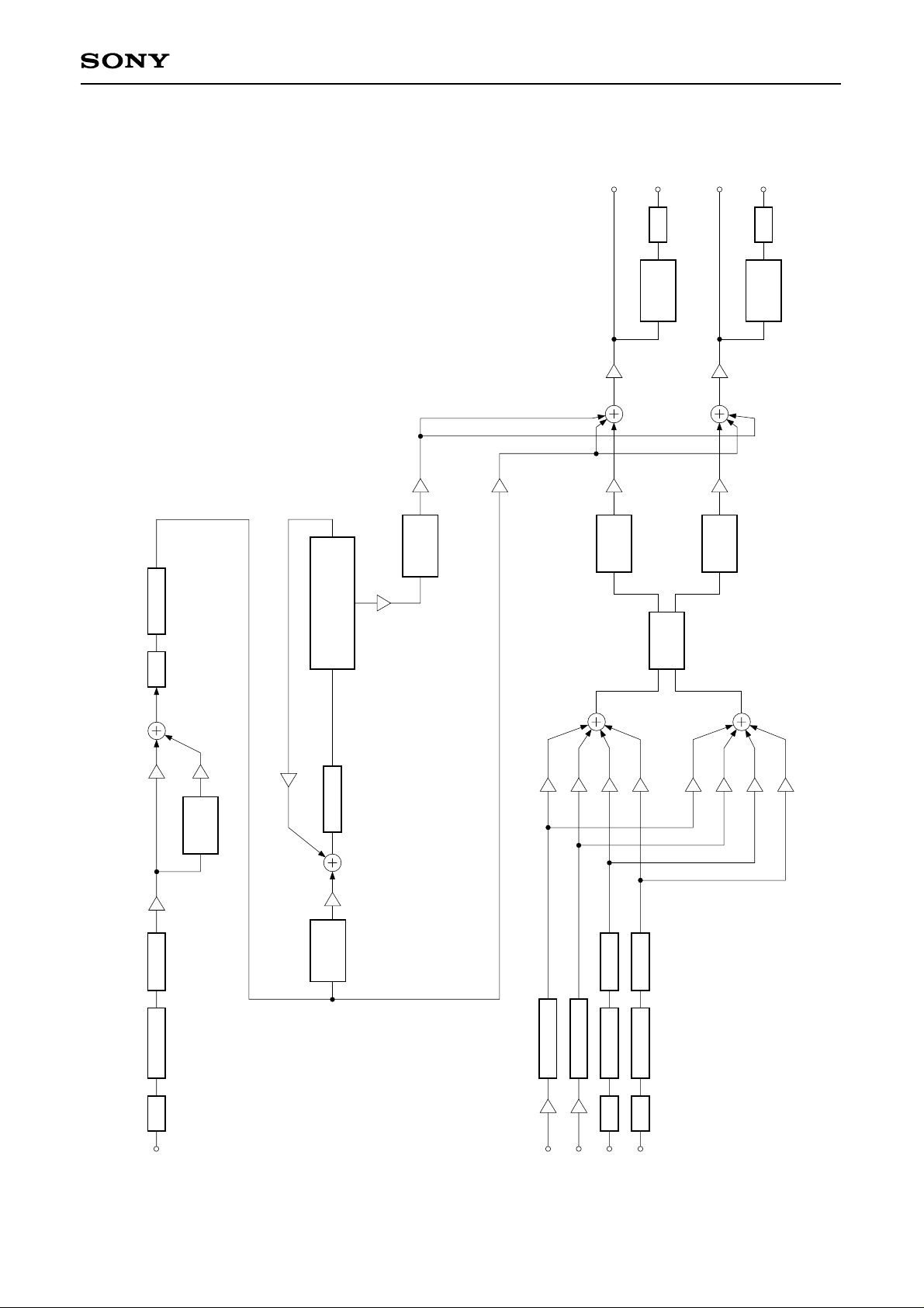
CXD2720Q
39H36H35H
High Cut1PEQ
3BH3AH
38H37H
44H
TdoTdi
47H
Tre
Delay Line
45H –Kre
–Keff
Over
3DH
Sampling
–Kdry
3CH
SO1
–KLo
–KLm
Pitch
40H
3EH
Control
10H
DA1
DAC
Over
Sampling
2EH22H
Voice
Cancel
–KRo
–KRm
18H11H
SO2
Pitch
42H
3FH
Control
DA2
DAC
Over
Sampling
5BH
5AH
–Krmc
–Krmp
Pitch
Control
31H34H33H
–Kimc
DC Cut2
DecimationADC
MIC
13. DSP Signal Flow
53H
4AH
–Kfb
High Cut2
–Krd
Down
Sampling
4DH
4CH4BH
49H
–KisLm05H
–KisRc06H
04H
DeEmphasis
–Ki
–Ki 00H
SI1
–KiaLm07H
–KiaRc08H
DC Cut1DecimationADC
DeEmphasis
SI2
AD1
0FH0EH
DC Cut1
DecimationADC
AD2
–KisLc0AH
–KisRm09H
–KiaLc0CH
–KiaRm0BH
Refer to the coefficient RAM setting for information on each coefficient.
∗
– 33 –
Page 34
CXD2720Q
14. Filter Coefficient Table
[Relevant coefficient] DC1f0 (address = 0FH), DC2f0 (address = 33H), HC1b (address = 3BH),
HC1a1 (address = 39H), HC1a0 (address = 3AH), HC2b (address = 4DH),
HC2a1 (address = 4BH), HC2a0 (address = 4CH), PEQa (address = 35H),
PEQb1 (address = 36H), PEQb2 (address = 37H), PEQg (address = 38H)
The cut-off frequencies and PEQ gain, Q, and center frequency settings for each signal flow filter are shown in
Tables 13-1 to 13-5.
Note that if the above setting values are changed during DSP operation, the output level becomes unstable for
several 1/fs.
Tables 14-1 to 14-5 and digital de-emphasis are given for fs = 44.1kHz. Please inquire with regard to using an
fs other than this value.
(1) DC Cut1 for Accompaniment/ DC Cut2 for Voice
Cut-off
frequency (Hz)
20
30
40
50
60
70
80
90
100
110
120
130
140
150
160
170
180
190
200
210
220
230
240
250
260
DC1f0
DC2f0
7FA2
7F74
7F45
7F17
7EE9
7EBA
7E8C
7E5E
7E30
7E02
7DD4
7DA6
7D78
7D4B
7D1D
7CEF
7CC2
7C94
7C67
7C39
7C0C
7BDF
7BB2
7B85
7B58
Cut-off
frequency (Hz)
270
280
290
300
310
320
330
340
350
360
370
380
390
400
410
420
430
440
450
460
470
480
490
500
510
DC1f0
DC2f0
7B2B
7AFE
7AD1
7AA4
7A77
7A4B
7A1E
79F1
79C5
7998
796C
7940
7914
78E7
78BB
788F
7863
7837
780B
77DF
77B4
7788
775C
7731
7705
Cut-off
frequency (Hz)
520
530
540
550
560
570
580
590
600
610
620
630
640
650
660
670
680
690
700
710
720
730
740
750
760
DC1f0
DC2f0
76D9
76AE
7683
7657
762C
7601
75D6
75AB
7580
7555
752A
74FF
74D4
74A9
747E
7454
7429
73FF
73D4
73AA
737F
7355
732B
7301
72D6
Cut-off
frequency (Hz)
770
780
790
800
810
820
830
840
850
860
870
880
890
900
910
920
930
940
950
960
970
980
990
1000
DC1f0
DC2f0
72AC
7282
7258
722E
7204
71DB
71B1
7187
715D
7134
710A
70E1
70B7
708E
7064
703B
7012
6FE9
6FBF
6F96
6F6D
6F44
6F1B
6EF2
Table 14-1.
– 34 –
Page 35
(2) High Cut1 for Voice
CXD2720Q
Cut-off
frequency (Hz)
1000
1100
1200
1300
1400
1500
1600
1700
1800
1900
2000
2100
2200
2300
2400
2500
2600
2700
2800
2900
3000
3100
3200
3300
3400
3500
3600
3700
3800
3900
4000
4100
4200
4300
4400
4500
4600
4700
4800
4900
5000
5100
5200
5300
5400
5500
HC1b HC1a1 HC1a0
6EF2
6D5C
6BCB
6A3E
68B6
6733
65B4
6439
62C3
6150
5FE2
5E77
5D11
5BAE
5A4E
58F2
579A
5645
54F3
53A4
5259
5110
4FCB
4E88
4D48
4C0B
4AD0
4998
4863
4730
4600
44D2
43A6
427C
4155
4030
3F0D
3DEC
3CCD
3BAF
3A94
397B
3863
374D
3639
3527
0886
0951
0A1A
0AE0
0BA4
0C66
0D25
0DE3
0E9E
0F57
100E
10C4
1177
1228
12D8
1386
1432
14DD
1586
162D
16D3
1777
181A
18BB
195B
19FA
1A97
1B33
IBCE
1C67
1CFF
1D96
1E2C
1EC1
1F55
1FE7
2079
2109
2199
2228
22B5
2342
23CE
2459
24E3
256C
F77A
F6AF
F5E6
F520
F45C
F39A
F2DB
F21D
F162
F0A9
EFF2
EF3C
EE89
EDD8
ED28
EC7A
EBCE
EB23
EA7A
E9D3
E92D
E889
E7E6
E745
E6A5
E606
E569
E4CD
E432
E399
E301
E26A
E1D4
E13F
E0AB
E019
DF87
DEF7
DE67
DDD8
DD4B
DCBE
DC32
DBA7
DB1D
DA94
Cut-off
frequency (Hz)
5600
5700
5800
5900
6000
6100
6200
6300
6400
6500
6600
6700
6800
6900
7000
7100
7200
7300
7400
7500
7600
7700
7800
7900
8000
8100
8200
8300
8400
8500
8600
8700
8800
8900
9000
9100
9200
9300
9400
9500
9600
9700
9800
9900
10000
OFF
HC1b HC1a1 HC1a0
3416
3306
31F9
30EC
2FE2
2ED8
2DD0
2CCA
2BC4
2AC0
29BD
28BC
27BB
26BC
25BD
24C0
23C4
22C9
21CF
20D5
1FDD
1EE6
1DEF
1CF9
1C04
1B10
1A1C
192A
1838
1746
1655
1565
1475
1386
1298
11A9
10BC
0FCF
0EE2
0DF5
0D09
0C1E
0B32
0A47
095C
0000
25F4
267C
2703
2789
280E
2893
2917
299A
2A1D
2A9F
2B21
2BA1
2C22
2CA1
2D21
2D9F
2E1D
2E9B
2F18
2F95
3011
308C
3108
3183
31FD
3277
32F1
336A
33E3
345C
34D5
354D
35C5
363C
36B3
372B
37A1
3818
388E
3905
397B
39F0
3A66
3ADC
3B51
0000
DA0C
D984
D8FD
D877
D7F2
D76D
D6E9
D666
D5E3
D561
D4DF
D45F
D3DE
D35F
D2DF
D261
D1E3
D165
D0E8
D06B
CFEF
CF74
CEF8
CE7D
CE03
CD89
CD0F
CC96
CC1D
CBA4
CB2B
CAB3
CA3B
C9C4
C94D
C8D5
C85F
C7E8
C772
C6FB
C685
C610
C59A
C524
C4AF
8000
Table 14-2.
– 35 –
Page 36

(3) High Cut2 for Microphone Echo
CXD2720Q
Cut-off
frequency (Hz)
1000
1100
1200
1300
1400
1500
1600
1700
1800
1900
2000
2100
2200
2300
2400
2500
2600
2700
2800
2900
3000
3100
3200
3300
3400
3500
3600
3700
3800
3900
4000
4100
4200
4300
4400
4500
4600
4700
4800
4900
5000
5100
5200
5300
5400
5500
HC2b HC2a1 HC2a0
5FE2
5D11
5A4E
579A
54F3
5259
4FCB
4D48
4AD0
4863
4600
43A6
4155
3F0D
3CCD
3A94
3863
3639
3416
31F9
2FE2
2DD0
2BC4
29BD
27BB
25BD
23C4
21CF
1FDD
1DEF
1C04
1A1C
1838
1655
1475
1298
10BC
0EE2
0D09
0B32
095C
0788
05B3
03E0
020D
003A
100E
1177
12D8
1432
1586
16D3
181A
195B
1A97
1BCE
1CFF
1E2C
1F55
2079
2199
22B5
23CE
24E3
25F4
2703
280E
2917
2A1D
2B21
2C22
2D21
2E1D
2F18
3011
3108
31FD
32F1
33E3
34D5
35C5
36B3
37A1
388E
397B
3A66
3B51
3C3B
3D26
3E0F
3EF9
3FE2
EFF2
EE89
ED28
EBCE
EA7A
E92D
E7E6
E6A5
E569
E432
E301
E1D4
E0AB
DF87
DE67
DD4B
DC32
DB1D
DA0C
D8FD
D7F2
D6E9
D5E3
D4DF
D3DE
D2DF
D1E3
D0E8
CFEF
CEF8
CE03
CD0F
CC1D
CB2B
CA3B
C94D
C85F
C772
C685
C59A
C4AF
C3C5
C2DA
C1F1
C107
C01E
Cut-off
frequency (Hz)
5600
5700
5800
5900
6000
6100
6200
6300
6400
6500
6600
6700
6800
6900
7000
7100
7200
7300
7400
7500
7600
7700
7800
7900
8000
8100
8200
8300
8400
8500
8600
8700
8800
8900
9000
9100
9200
9300
9400
9500
9600
9700
9800
9900
10000
OFF
HC2b HC2a1 HC2a0
FE68
FC95
FAC2
F8EE
F719
F543
F36C
F194
EFBB
EDE0
EC02
EA23
E841
E65D
E476
E28C
E09F
DEAE
DCBA
DAC1
D8C5
D6C4
D4BE
D2B3
D0A3
CE8E
CC72
CA50
C828
C5F9
C3C2
C184
BF3E
BCEF
BA98
B837
B5CC
B357
B0D7
AE4C
ABB5
A911
A660
A3A1
A0D4
0000
40CC
41B5
429F
4389
4473
455E
464A
4736
4822
4910
49FF
4AEE
4BDF
4CD1
4DC5
4EBA
4FB0
50A9
51A3
529F
539D
549E
55A1
56A6
57AE
58B9
59C7
5AD8
5BEC
5D03
5E1F
5F3E
6061
6188
62B4
63E4
651A
6654
6794
68DA
6A25
6B77
6CD0
6E2F
6F96
0000
BF34
BE4B
BD61
BC77
BB8D
BAA2
B9B6
B8CA
B7DE
B6F0
B601
B512
B421
B32F
B23B
B146
B050
AF57
AE5D
AD61
AC63
AB62
AA5F
A95A
A852
A747
A639
A528
A414
A2FD
A1E1
A0C2
9F9F
9E78
9D4C
9C1C
9AE6
99AC
986C
9726
95DB
9489
9330
91D1
906A
8000
Table 14-3.
– 36 –
Page 37
(4) PEQ for Voice
CXD2720Q
Center
frequency (Hz)
250.0
280.6
315.0
353.6
396.9
445. 4
500. 0
561.2
630.0
707.1
793.7
890.9
1000. 0
1122.5
1259.9
1414.2
1587.4
1781.8
2000.0
2244.9
2519.8
2828.4
3174.8
3563.6
4000.0
4489.8
5039.7
5656.9
6349.6
7127.2
8000.0
PEQa PEQb1 PEQb2
023D
0282
02CF
0325
0385
03F0
0467
04EC
0580
0624
06DB
07A6
0886
097E
0A91
0BC0
0D0D
0E7C
100E
11C7
13A8
15B5
17F1
1A5E
1CFF
1FD8
22ED
2642
29DB
2DC1
31FD
7DAE
7D64
7D10
7CB2
7C47
7BCF
7B48
7AAE
7A01
793D
785E
7762
7643
74FD
738B
71E5
7004
6DE0
6B6D
68A1
656E
61C6
5D97
58CF
535A
4D24
4617
3E23
353B
2B5C
2097
847B
8505
859F
864B
870B
87E1
88CF
89D9
8B01
8C4A
8DB7
8F4D
910E
92FE
9524
9781
9A1C
9CFA
A01E
A38F
A752
AB6C
AFE4
B4BE
BA00
BFB2
C5DC
CC85
D3B8
DB84
E3FC
Gain (dB)
0.0
0.5
1.0
1.5
2.0
2.5
3.0
3.5
4.0
4.5
5.0
5.5
6.0
6.5
7.0
7.5
8.0
8.5
9.0
9.5
10.0
10.5
11.0
11.5
12.0
Table 14-5.
PEQg
0000
01E5
03E7
0608
0849
0AAC
0D33
0FE1
12B7
15B8
18E7
1C46
1FD9
23A1
27A3
2BE2
3061
3524
3A30
3F88
4531
4B30
518A
5844
5F64
Table 14-4.
– 37 –
Page 38
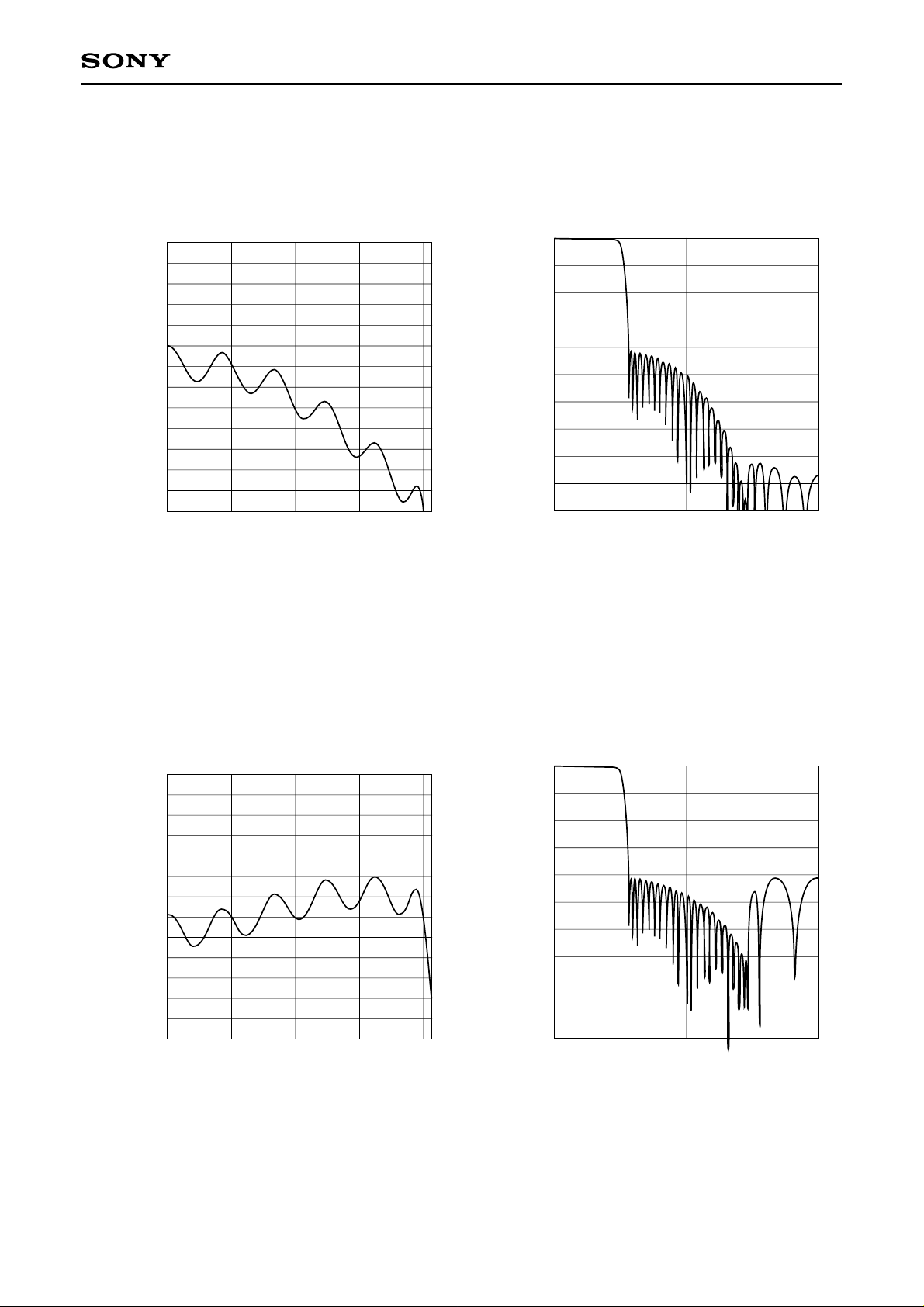
Filter Characteristics
ADC Filter Characteristics (43rd + 15th FIR)
CXD2720Q
]
–3
–100.00
–200.00
–300.00
–400.00
Response [dB × 10
–500.00
–600.00
–700.00
–800.00
500.00
400.00
300.00
200.00
100.00
0.00
Pass band
0.00
–10.00
–20.00
–30.00
–40.00
–50.00
–60.00
Response [dB]
–70.00
–80.00
–90.00
0
10515
Frequency [kHz]
20
–100.00
Stop band
1fs
Frequency [kHz]
2fs
DAC Filter Characteristics (43rd + 7th FIR)
Pass band
500.00
400.00
300.00
200.00
]
–3
100.00
0.00
–100.00
–200.00
–300.00
–400.00
Response [dB × 10
–500.00
–600.00
–700.00
–800.00
0
10 20515
Frequency [kHz]
0.00
–10.00
–20.00
–30.00
–40.00
–50.00
–60.00
Response [dB]
–70.00
–80.00
–90.00
–100.00
Stop band
1fs 2fs
Frequency [kHz]
– 38 –
Page 39
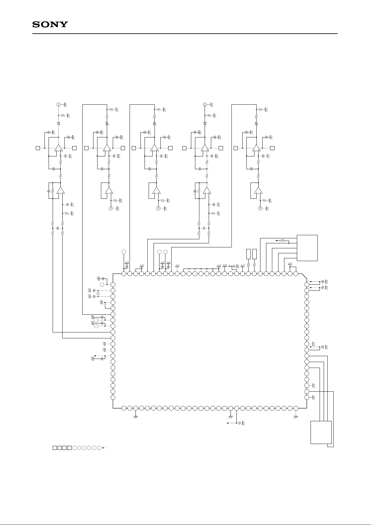
CXD2720Q
CH2 OUT
AGND
330k
AGND
10µ2
0.01
2
100p
0.01
AGND
1
4
8
3
220p
10k10k
1000p
7
39k
6
5
100p39k
12k22k
12k22k
220p
: AD operational amplifier +12V power supply
: DA operational amplifier +12V power supply
: AD operational amplifier –12V power supply
: DA operational amplifier –12V power supply
1
234
1M
AGND
4.7k
10µ2
0.01
AGND
4
1
AGND
AGND AGND
AGND
20p20p
AGNDAGND
CF
DGND AGNDAGND
: Crystal oscillator circuit +5V power supply
: AIN1 +5V power supply
: AIN2 +5V power supply
: AIN3 +5V power supply
B
C
D
: AO1 +5V power supply
E
A
0.01
AGND
1
4
8
3
1.8k1.8k
1200p
2200p
7
6
5
100k
CH2 IN
0.01
DD
A
31
768fs
32
33
SS
34
AGND
: AO2 +5V power supply
F
S2
35
36
D2
0.01
37
D5
0.01
38
39
40
S5
4142
AGNDDGND
SS
3
DD
1
43
NC
44
0.01
NC
45
NC
46
NC
47
NC
48
NC
49
NC
50
: Digital power supply + 5V
5532 operational amplifier used
3
AGND
AGND
AGND
B
0.01
30
XV
XTLO
XTLI
XV
AV
AIN2
AV
AV
AO2N
AO2P
AV
V
V
NC
51
AGND
AGND
D1
AV
29
AIN1
NC
52
CH1 OUT
1M
AGND
4.7k
10µ2
0.01
1
AGND
28
27
S1
AVS4AV
SS4
NC
V
54
53
DGND
2200p
26
AO1N
NC
55
8
AGND
1
1.8k1.8k
7
6
25
AO1P
NC
56
4
3
CH1 IN
E
0.01
24
NC
57
1200p
5
AGND
0.01
100k
D
23
D3AVD4
AV
NC
58
AGND
3
AGND
AGND
AGND
AGND
0.01
22
AIN3
NC
59
AGND
21
S3
AV
NC
60
0.01
2
100p
12k22k
20
18
19
SS2
V
TST4
TST5
NC
NC
NC
63
61
62
10µ2
8
1000p
39k
17
TST3
NC
64
AGND
16
10k10k
7
220p
330k
4
3
220p
5
12k22k
16
TST2
CXD2720Q
NC
65
100p39k
15
TST1
NC
66
AGND
AGND
0.01
4
AGND
DGND
14
TST0
NC
67
AGND
AGND AGND
13
XS24
NC
68
DGND
1
DGND
0.01
11
12
SO
DD0
V
DD2VSS5
V
69
70
DGND
0.01
DGND
10
SS1
V
NC
71
0.01
XRST
9
XRST
NC
72
DGND
4.7k
10µ2
AGND
1
8
2200p
6
XWO
8
XWO
NC
73
1.8k1.8k
7
1M
4
3
5
CH3 IN
7
TRDT
NC
74
1200p
100k
0.01
6
REDY
NC
75
AGND
3
AGND
AGND
5
XLAT
NC
76
AGND
AGND
4
SCK
NC
77
3
RVDT
NC
78
Application circuits shown are typical examples illustrating the operation of
the devices. Sony cannot assume responsibility for any problems arising out
of the use of these circuits or for any infringement of third party patent and
other right due to same.
Microcomputer
DGND
2
1
SS0
V
AVS0
AV
D0
100
V
DD
3
99
NC
98
NC
97
NC
96
NC
95
NC
94
NC
93
NC
92
NC
91
V
SS7
XMST
LRCK
BCK
SI
NC
NC
INVI
BFOT
X768
SS6
NC
V
79
80
DGND
90
89
88
87
86
85
84
83
82
81
DGND DGND DGND
SIN
BCK
DA16
CXD2500Q
0.01 0.01 0.01
DA15
DGND DGND DGND
LRCK
LRCKXTAI
Application Circuit
– 39 –
Page 40

Package Outline Unit: mm
100PIN QFP (PLASTIC)
23.9 ± 0.4
+ 0.4
20.0 – 0.1
+ 0.4
17.9 ± 0.4
14.0 – 0.01
+ 0.1
0.15 – 0.05
15.8 ± 0.4
CXD2720Q
A
0.65
SONY CODE
EIAJ CODE
JEDEC CODE
0° to 15°
±0.12
DETAIL A
QFP-100P-L01
∗QFP100-P-1420-A
M
0.15
(16.3)
0.8 ± 0.2
2.75 – 0.15
PACKAGE STRUCTURE
PACKAGE MATERIAL
LEAD TREATMENT
LEAD MATERIAL
PACKAGE WEIGHT
EPOXY RESIN
SOLDER PLATING
COPPER / 42 ALLOY
1.4g
+ 0.35
– 40 –
 Loading...