

Page 1

CD Digital Signal Processor
Description
The CXD2500BQ is a digital signal processing LSI
designed for use in compact disc players. It has the
following functions:
• Wide-frame jitter margin (±28 frames) realized by a
built-in 32K RAM.
• Bit clock generated by digital PLL for strobing EFM
signals. Capture range of ±150 kHz and over.
• EFM data demodulation
• Enhanced protection of EFM Frame Sync signals
• Powerful error correction based on Refined Super
Strategy
Error correction C1: Double correction
C2: Quadruple correction
• Double-speed playback and vari-pitch playback
• Reduced noise generation at track jump
• Auto zero-cross muting
• Subcode demodulation and subcode Q data error
detection
• Digital spindle servo system (incorporating an
oversampling filter)
• 16-bit traverse counter
• Built-in asymmetry correction circuit
• CPU interface using a serial bus
• Servo auto sequencer
• Output for digital audio interface
• Built-in digital level meter and peak meter
• Bilingual
CXD2500BQ
80 pin QFP (Plastic)
Features
• All digital signals for regeneration are processed
using one chip.
• The built-in RAM enables high-integration
mounting.
Structure
Silicon-gate CMOS IC
Sony reserves the right to change products and specifications without prior notice. This information does not convey any license by
any implication or otherwise under any patents or other right. Application circuits shown, if any, are typical examples illustrating the
operation of the devices. Sony cannot assume responsibility for any problems arising out of the use of these circuits.
—1—
E91Y46F64-TE
Page 2

CXD2500BQ
Absolute Maximum Ratings (Ta=25 °C)
• Supply voltage VCC –0.3 to +7.0 V
• Input voltage VI –0.3 to +7.0 V
• Output voltage VO –0.3 to +7.0 V
• Operating temperature Topr –20 to +75 °C
• Storage temperature Tstg –40 to +125 °C
• Supply voltage differences VSS–AVSS –0.3 to +0.3 V
VDD–AVDD –0.3 to +0.3 V
Recommended Operating Conditions
• Supply voltage VDD 4.75∗1to 5.25∗3(5.0 V typ.) V
• Operating temperature Topr –20 to +75 °C
• Input voltage VIN VSS–0.3 to + VDD + 0.3 V
∗1
VDD value of 4.75 V (min.) is for the double-speed playback mode at vari-pitch control reset. For the low
power consumption special playback mode, VDD value is 3.6 V (min.). ∗2In the normal-speed playback
mode VDD value is 4.5 V (min.)
∗2
Low power consumption, special playback mode
Set the internal operation of LSI at the double-speed mode, and half the crystal oscillation frequency. This
will result in the normal-speed playback mode.
∗3
VDD value of 5.25 V (max.) is for the double-speed playback mode at vari-pitch control reset. For normalspeed playback and the low power consumption special playback mode, the VDD value is 5.5 V (max.).
I/O Capacity
• Input pins CI 12 pF max.
• Output pins CO 12 pF max. at high impedance
Note: Test Conditions
VDD=VI=0 V
fM=1 MHz
—2—
Page 3
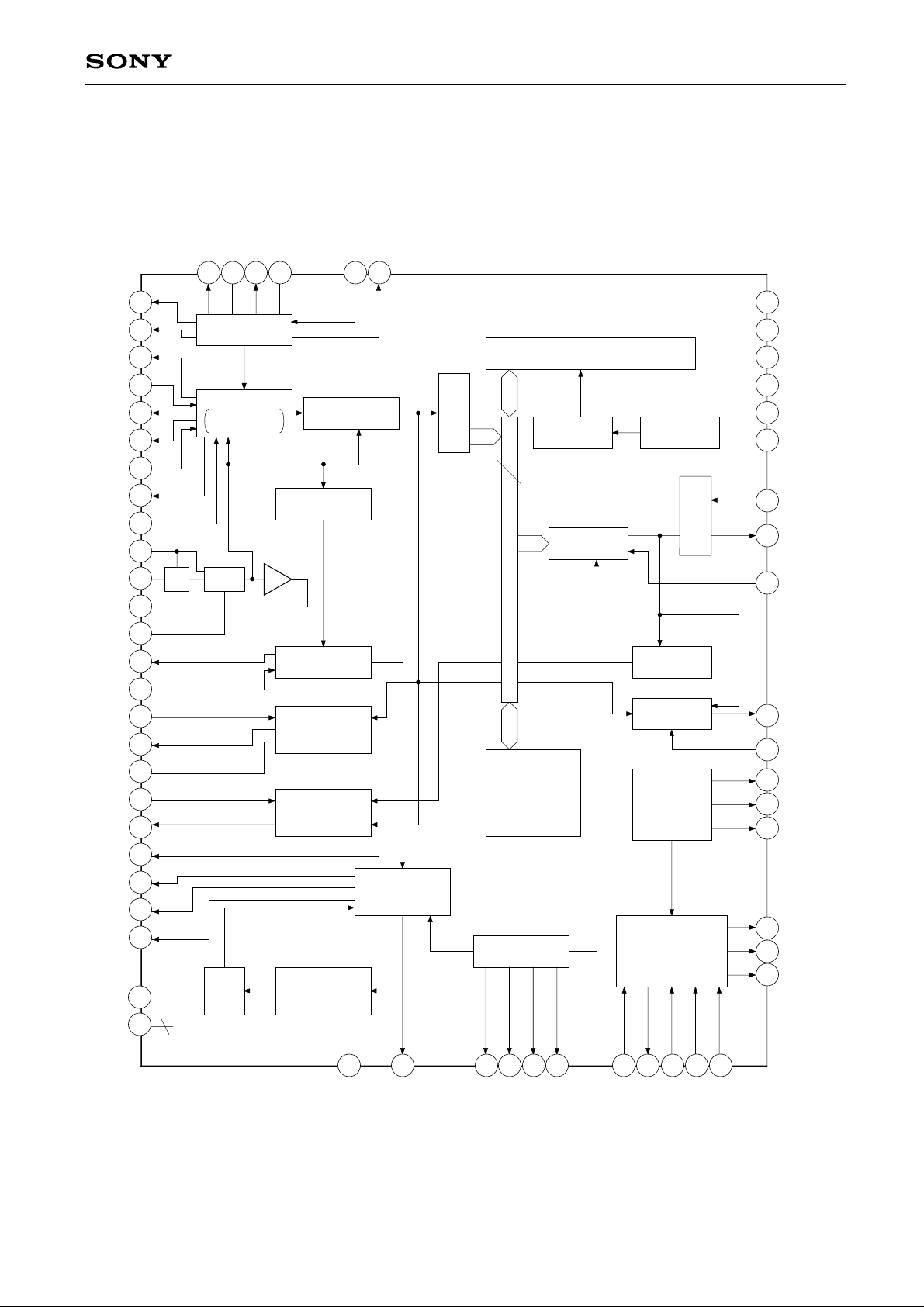
Block Diagram
CXD2500BQ
C4M
C16M
PDO
VCO1
VCO0
PCO
FIL1
FIL0
CLTV
RF
ASY1
ASY0
ASYE
WFCK
SCOR
EXCK
SBSO
EMPH
SQCK
SQSO
MON
FSW
MDP
MDS
TEST
NC
57
58
11
9
8
20
19
18
22
24
26
27
28
62
63
65
64
61
67
66
3
2
4
43
10
FSTT
generator
Digital PLL
vari-pitch
double speed
∗ MUX
Noise
shaper
5
XTAO
XTAI
Clock
XTSL
535456 53 17 19
EFM
demodulator
Sync
Protector
Timing
Generator
Subcode
P-W
Processor
Subcode
Q
Processor
18-times
over samplling
filter
70
VCKI
VPCO
CLV
processor
6
Register
8
Error corrector
Timing
Generator 2
32K RAM
Address
generator
D/A
data processor
313250 51
Priority
encoder
Serial/Parallel
Peak detector
Digital out
CPU interface
Servo
auto
sequencer
6975 76 80
processor
1
23
AV
21
AVSS
33
VDD
73
VDD
12
VSS
52
VSS
30
PSSL
49
DAO 1 to 6
MUTE
68
60
DOUT
MD 2
59
71
DATA
74
CLOK
72
XLAT
DATO
77
79
CLKO
78
XLTO
∗Asymmetry
correction.
DD
XRST
LOCK
—3—
APTR
APTL
LRCK
WDCK
SEIN
SENS
MIRR
CNIN
FOX
Page 4
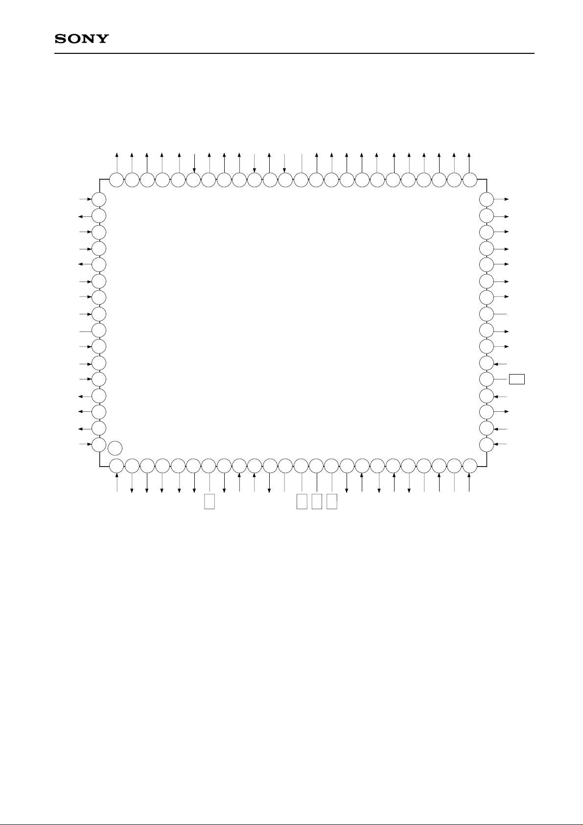
Pin Configuration
CXD2500BQ
EXCK
SQSO
SQCK
MUTE
SENS
XRST
DATA
XLAT
V
CLOK
SEIN
CNIN
DATO
XLTO
CLKO
MIRR
SBSO
SCOR
WFCK
EMPH
DOUT
MD2
C16M
C4M
FSTT
XTSL
XTAQ
XTAI
SS
V
APLL
APTR
DA01
DA02
DA03
DA04
DA05
DA06
DA07
DA08
DA09
414243444546474849505152535455565759 586061626364
65
66
67
68
69
70
71
72
73
DD
D2500B
74
75
76
77
78
79
80
40
39
38
37
36
35
34
33
32
31
30
29
28
27
26
25
DA10
DA11
DA12
DA13
DA14
DA15
DA16
DD
V
LRCK
WDCK
PSSL
NC
ASYE
ASYO
ASYI
BIAS
1 2 3 4 5 6 7 8 9 10 11 12 13 14 15 16 17 18 20 21 22 23 2419
SS
FOK
FSW
MON
MDP
MDS
LOCK
NC
VCOO
VCOI
TEST
PDO
NC
V
NC
NC
VPCO
VCKI
FILO
FILI
PCO
SS
AV
CLTV
DD
AV
RF
—4—
Page 5
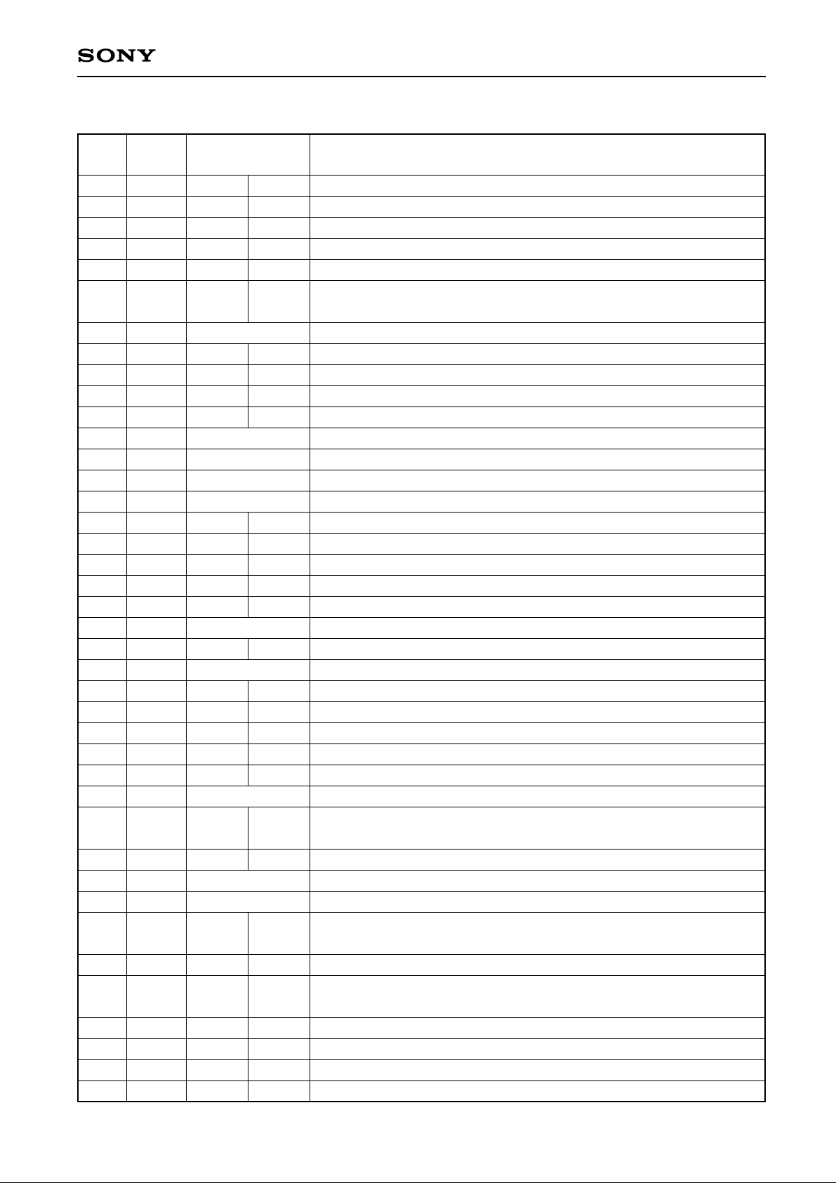
Pin Description
Pin
Symbol I/O Description
No.
1
2
3
4
5
6
7
8
9
10
11
12
13
14
15
16
17
18
19
20
21
22
23
24
25
26
27
28
29
30
31
32
33
34
35
36
37
38
39
40
FOK
FSW
MON
MDP
MDS
LOCK
NC
VCOO
VCOI
TEST
PDO
VSS
NC
NC
NC
VPCO
VCKI
FILO
FILI
PCO
AVSS
CLTV
AVDD
RF
BIAS
ASYI
ASYO
ASYE
NC
PSSL
WDCK
LRCK
VDD
DA16
DA15
DA14
DA13
DA12
DA11
DA10
I
O Z, 0
O 1, 0
O 1, Z, 0
O 1, Z, 0
O 1, 0
—
O 1, 0
I
I
O 1, Z, 0
—
—
—
O 1, Z, 0
I
O Analog
I
O 1, Z, 0
I
I
I
I
O 1, 0
I
—
I
O 1, 0
O 1, 0
O 1, 0
O 1, 0
O 1, 0
O 1, 0
O 1, 0
O 1, 0
O 1, 0
CXD2500BQ
Focus OK input. Used for SENS output and servo auto sequencer.
Output used to switch the spindle motor output filter.
Output for spindle motor ON/OFF control
Output for spindle motor servo control
Output for spindle motor servo control
Output is “H” when the GFS signal sampled at 460 Hz is “H”. Output is
“L” when the GFS signal is “L” 8 or more times in succession.
Output of oscillation circuit for analog EFM PLL
Input to oscillation circuit for analog EFM PLL fLOCK=8.6436 MHz
Test. Normally at 0 V (GND).
Output of charge pump for analog EFM PLL
GND
Output of charge pump for vari-pitch PLL
Clock input from external VCO for vari-pitch control. fc center=16.9344 MHz.
Output of filter for master PLL (Slave=Digital PLL)
Input to filter for master PLL
Output of charge pump for master PLL
Analog GND
VCO control voltage input for master PLL
Analog power supply (+5 V)
EFM signal input
Asymmetry circuit constant current input
Asymmetry comparator circuit voltage input
EFM full-swing output
Asymmetry circuit OFF at “L”. Asymmetry circuit ON at “H”.
Input used to switch the audio data output mode. “L” for serial output,
“H” for parallel output.
D/A interface for 48-bit slot. Word clock f=2Fs
D/A interface for 48-bit slot. LR clock f=Fs
Power supply (+5 V)
Outputs DA16 (MSB) when PSSL=1, or serial data from the 48-bit slot
(2’s complements, MSB first) when PSSL=0.
Outputs DA15 when PSSL=1, or bit clock from the 48-bit slot when PSSL=0.
Outputs DA14 when PSSL=1, or serial data from the 64-bit slot (2’s
complements, LSB first) when PSSL=0.
Outputs DA13 when PSSL=1, or bit clock from the 64-bit slot when PSSL=0.
Outputs DA12 when PSSL=1, or LR clock from the 64-bit slot when PSSL=0.
Outputs DA11 when PSSL=1, or GTOP when PSSL=0.
Outputs DA10 when PSSL=1, or XUGF when PSSL=0.
—5—
Page 6
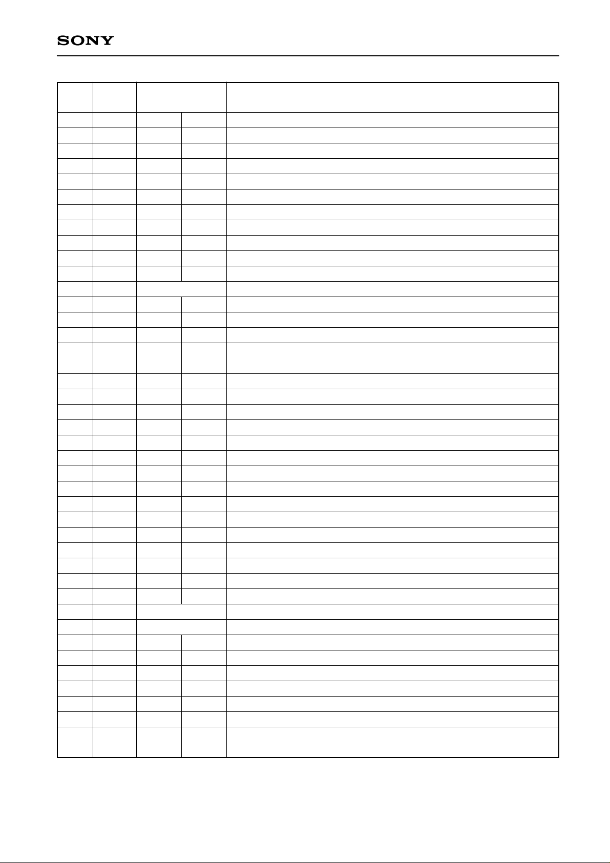
Pin
No.
41
42
43
44
45
46
47
48
49
50
51
52
53
54
55
56
57
58
59
60
61
62
63
64
65
66
67
68
69
70
71
72
73
74
75
76
77
78
79
80
Symbol I/O Description
DA09
DA08
DA07
DA06
DA05
DA04
DA03
DA02
DA01
APTR
APTL
VSS
XTAI
XTAO
XTSL
FSTT
C4M
C16M
MD2
DOUT
EMPH
WFCK
SCOR
SBSO
EXCK
SQSO
SQCK
MUTE
SENS
XRST
DATA
XLAT
VDD
CLOCK
SEIN
CNIN
DATO
XLTO
CLKO
MIRR
O 1, 0
O 1, 0
O 1, 0
O 1, 0
O 1, 0
O 1, 0
O 1, 0
O 1, 0
O 1, 0
O 1, 0
O 1, 0
I
O 1, 0
I
O 1, 0
O 1, 0
O 1, 0
I
O 1, 0
O 1, 0
O 1, 0
O 1, 0
O 1, 0
I
O 1, 0
I
I
— 1, Z, 0
I
I
I
I
I
I
O 1, 0
O 1, 0
O 1, 0
I
Outputs DA9 when PSSL=1, or XPLCK when PSSL=0.
Outputs DA8 when PSSL=1, or GFS when PSSL=0.
Outputs DA7 when PSSL=1, or RFCK when PSSL=0.
Outputs DA6 when PSSL=1, or C2PO when PSSL=0.
Outputs DA5 when PSSL=1, or XRAOF when PSSL=0.
Outputs DA4 when PSSL=1, or MNT3 when PSSL=0.
Outputs DA3 when PSSL=1, or MNT2 when PSSL=0.
Outputs DA2 when PSSL=1, or MNT1 when PSSL=0.
Outputs DA1 when PSSL=1, or MNT0 when PSSL=0.
Control output for aperture correction. “H” for R-ch.
Control output for aperture correction. “H” for L-ch.
GND
Input for 16.9344 MHz and 33.8688 MHz X'tal oscillation circuit.
Output for 16.9344 MHz X'tal oscillation circuit.
X'tal selection input. “L” for 16.9344 MHz X'tal, “H” for 33.8688 MHz X'tal.
2/3 frequency demultiplication output for Pins 53 and 54. Unaffected by
vari-pitch control.
4.2336 MHz output. Subject to vari-pitch control.
16.9344 MHz output. Subject to vari-pitch control.
Digital-Out ON/OFF control. “H” for ON, “L” for OFF.
Digital-Out output.
“H” for playback disc provided with emphasis, “L” for without emphasis.
WFCK (Write Frame Clock) output.
“H” when subcode Sync S0 or S1 is detected.
Serial output of Sub P to W
Clock input for reading SBSO
Outputs 80-bit Sub Q and 16-bit PCM peak-level data.
Clock input for reading SQSO
“H” for muting, “L” for release.
SENS output to CPU
System reset. “L” for resetting.
Inputs serial data from CPU.
Latches serial data input from CPU at falling edge.
Power supply (+5 V)
Inputs serial data transfer clock from CPU.
Inputs SENSE from SSP.
Inputs track jump count signal.
Outputs serial data to SSP.
Latches serial data output to SSP at falling edge.
Outputs serial data transfer clock to SSP.
Inputs mirror signal to be used by auto sequencer when jumping 16 or
more tracks.
CXD2500BQ
—6—
Page 7

CXD2500BQ
Note:
• The data at the 64-bit slot is output in 2’s complements on an LSB-first basis. The data at the 48-bit slot is
output in 2’s complements on an MSB-first basis.
• GTOP monitors the state of Frame Sync protection. (“H”: Sync protection window released)
• XUFG is a negative Frame Sync pulse obtained from the EFM signal before Frame Sync protection is
effected..
• XPLCK is an inversion of the EFM PLL clock. The PLL is designed so that the falling edge of XPLCK
coincides with a change point of the EFM signal.
• The GFS signal turns “H” upon coincidence between Frame Sync and the timing of interpolation protection.
• RFCK is a signal generated at 136-µs periods using a crystal oscillator.
• C2PO is a signal to indicate data error.
• XRAOF is a signal issued when a jitter margin of ±28F is exceeded by the 32K RAM.
—7—
Page 8

CXD2500BQ
Electrical Character
DC characteristics (VDD=AVDD=5.0 V±5 %, VSS=AVSS=0 V, Topr=–20 to +75°C)
Item Condition Min. Typ. Max. Unit Related pins
Input voltage.
“H” level
Input voltage
“L” level.
Input voltage
“H” level
Input voltage
“L” level
VIH (1)
VIL (1)
VIN (2)
VIN (2)
Schmitt circuit
input
0.7VDD V
∗1
0.3VDD V
0.8VDD V
∗2
0.2VDD V
Input voltage
Output voltage
“H” level
Output voltage
“L” level
Output voltage
“H” level
Output voltage
“L” level
Output voltage
“L” level
Output voltage
“H” level
Output voltage
Output Output Output Output Input Input Input
voltage (4) voltage (3) voltage (2) voltage (1) voltage (3) voltage (2) voltage (1)
“L” level
Input leak current
VIN (3)
VOH (1)
VOL (1)
VOH (2)
VOL (2)
VOL (3)
VOH (4)
VOL (4)
ILI
Analog input
IOH=–1 mA
IOL=1 mA
IOH=–1 mA
IOL=2 mA
IOL=2 mA
IOH=–0.28 mA
IOL=0.36 mA
VI=0 to 5.25 V
VSS VDD V
VDD–0.5 VDD V
0 0.4 V
VDD–0.5 VDD V
0 0.4 V
0 0.4 V
VDD–0.5 VDD V
0 0.4 V
±5 µA
∗3
∗4
∗5
∗
6
∗
7
∗
1, ∗2, ∗3
Tristate pin output leak
current
ILO
VO=0 to 5.25 V
±5 µA
∗
8
Related pins
∗
1 XTSL, DATA, XLAT, MD2, PSSL
∗
2 CLOK, XRST, EXCK, SQCK, MUTE, FOK, SEIN, CNIN, MIRR, VCKI, ASYE
∗
3 CLTV, FILI, RF
∗
4 MDP, PDO, PCO, VPCO
∗
5 ASYO, DOUT, FSTT, C4M, C16M, SBSO, SQSO, SCOR, EMPH, MON, LOCK, WDCK, DATO, CLKO,
XLTO, SENS, MDS, DA01 to DA16, APTR, APTL, LRCK, WFCK
∗
6 FSW
∗
7 FILO
∗
8 SENS, MDS, MDP, FSW, PDO, PCO, VPCO
—8—
Page 9

AC Characteristics
(1) XTAI and VCOI pins
1) During self-oscillation (Topr=–20 to +75 °C, VDD=AVDD=5.0 V±5 %)
CXD2500BQ
Item
Oscillation frequency
Symbol
fMAX
Min.
7
Typ. Max.
34
Unit
MHz
2) With pulses input to XTAI and VCOI pins (Topr=–20 to +75 °C, VDD=AVDD=5.0 V±5 %)
Item
“H” level pulse width
“L” level pulse width
Pulse period
Input “H” level
Symbol
tWHX
tWLX
tCX
VIHX
Min.
13
13
26
VDD–1.0
Typ. Max.
500
500
1,000
Unit
ns
V
Input “L” level
Rising time
Falling time
VILX
tR, tF
0.8
10
ns
tCX
tWHX tWLX
XTAI
t
R
tF
3) With sine waves input to XTAI and VCOI pins via capacitor
Item
Input amplitude
Symbol
V1
Min.
2.0
VIHX
VIHX×0.9
VDD/2
VIHX×0.1
V
ILX
(Topr=–20 to +75 °C, VDD=AVDD=5.0 V±5 %)
Typ. Max.
VDD+0.3
Unit
Vp-p
—9—
Page 10
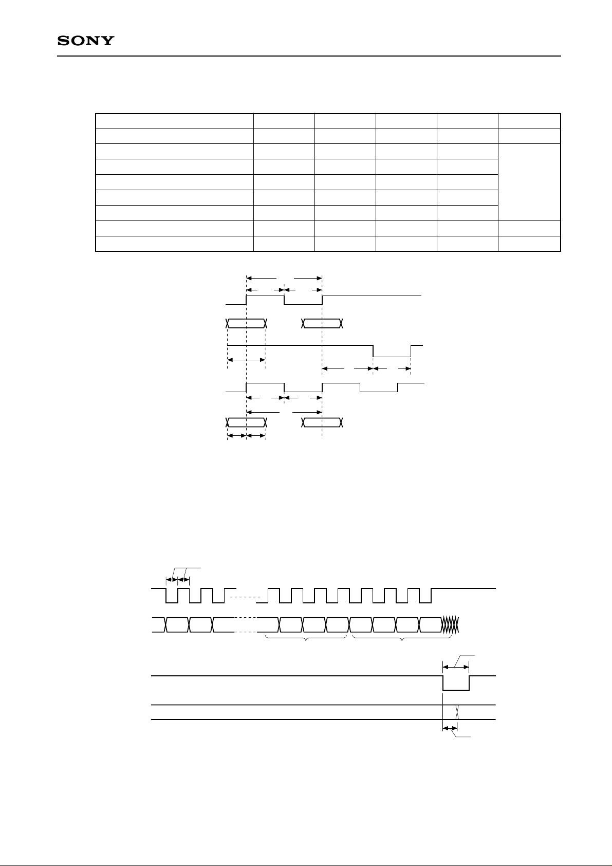
(1) CLOK, DATA, XLAT, CNIN, SQCK, and EXCK pins
(VDD=AVDD=5.0 V±5 %, VSS=AVSS=0 V, Topr=–20 to +75 °C
CXD2500BQ
Item
Clock frequency
Clock pulse width
Setup time
Hold time
Delay time
Latch pulse width
EXCK, CNIN, SQCK frequency
EXCK, CNIN, SQCK pulse width
CLOK
DATA
XLAT
EXCK
CNIN
SQCK
SUBQ
SQCK
tSU tH
tSU tH
Symbol
tWCK
tWCK
tWT
fCK
tSU
tH
tD
tWL
fT
tWT
1/fCK
1/fT
tWCK
tWT
Min.
750
300
300
300
750
300
tD tWL
Typ. Max.
0.65
1
Unit
MHz
ns
MHz
ns
Description of Functions
§1 CPU Interface and Commands
• CPU interface
This interface is used to set various modes using DATA, CLOK, and XLAT.
The interface timing chart is shown below.
750ns or more
CLOK
DATA
XLAT
Registers 4 to E
D1 D2 D3 D0 D1 D2 D3
Data Address
750ns or more
Valid
300ns max
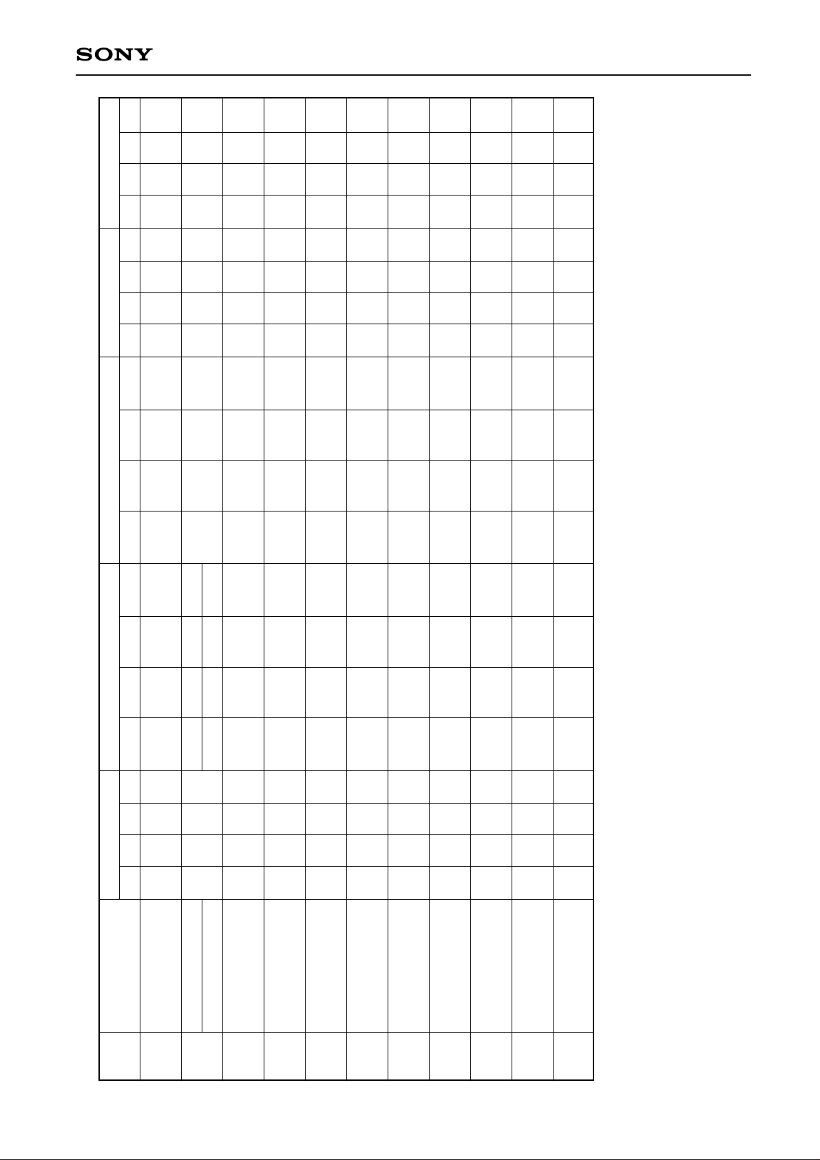
• The command addresses of the CXD2500B and the data capable of being set are shown in Table 1-1.
• When XRST is set to 0, the CXD2500B is reset, causing its internal registers to be initialized to the values
listed in Table 1-2.
—10—
Page 11
Data 4
CXD2500BQ
D3 D2 D1 D0
Data 3
D3 D2 D1 D0
Data 2
D3 D2 D1 D0
————
————
————
————
————
————
8421
————
————
————
128 64 32 16
2,048 1,024 512 256
————
————
————
WSEL
————
————
FLFC —
MAIN SUB
BiliGL BiliGL
8421
————
————
128 64 32 16
2,048 1,024 512 256
PCT1 PCT2 — —
————
————
————
————
————
————
————
————
————
CLVS
Table 1-1
Data 1
D3 D2 D1 D0
Address
D3 D2 D1 D0
Command
AS3 AS2 AS1 AS0
0.18 ms 0.09 ms 0.045 ms 0.022 ms
0.36 ms 0.18 ms 0.09 ms 0.045 ms
11.6 ms 5.8 ms 2.9 ms 1.45 ms
0100
Auto sequence
0101
0110
Blind (A, E), Overflow (C)
Brake (B)
KICK (D)
D OUT
Mute-F
32,768 16,384 8,192 4,096
0111
Auto sequencer track
jump (N) setting
D CLV DSPB A SEQ D PLL
CDROM 0
1000
MODE specification
ON-OFF ON-OFF ON-OFF ON-OFF
1001
Func specification
Mute ATT
UP Down
Vari Vari
1010
Audio CTRL
Traverse monitor
Gain Gain Gain Gain
32,768 16,384 8,192 4,096
1011
counter setting
MDP1 MDP0 MDS1 MDS0
1100
Servo factor setting
TB TP
DCLV
CM3 CM2 CM1 CM0
PWM MD Gain
1101
1110
CLV CRTL
CLV mode
name
Register
Commands
4
5
6
7
8
9
A
B
C
E
D
—11—
Page 12

Data 3
CXD2500BQ
D3 D2 D1 D0
Data 3
D3 D2 D1 D0
Data 2
D3 D2 D1 D0
————
————
————
————
————
————
0000
————
————
————
————
0000
————
0001
————
————
————
000—
0000
————
0000
————
00——
0001
————
————
————
————
————
————
————
————
————
Data 1
D3 D2 D1 D0
Address
D3 D2 D1 D0
Command
0000
0100
0101
0111
0000
0000
0101
0110
0111
1000
1001
0011
0000
1001
1010
1011
0110
1100
0000
1101
Table 1-2
0000
1110
Auto sequence
Blind (A, E), Overflow (C)
4
name
Register
Reset Initialization
Brake (B)
5
KICK (D)
Auto sequencer
6
track jump setting
MODE specification
7
8
Func specification
Audio CTRL
Traverse monitor
9
A
—12—
counter setting
Servo factor setting
B
C
CLV CRTL
CLV mode
E
D
Page 13

§1 Meanings of Data Set at Command Addresses
$4X Command
CXD2500BQ
Command
CANCEL
FOCUS-ON
1 TRACK JUMP
10 TRACK JUMP
2N TRACK JUMP
M TRACK MOVE
AS3
0
0
1
1
1
1
AS2
0
1
0
0
1
1
AS1
0
1
0
1
0
1
AS0
0
1
RXF
RXF
RXF
RXF
RXF=0 FORWARD
RXF=1 REVERSE
• If a Focus-ON command ($47) is canceled during execution, $02 is issued and the auto sequence operation
is discontinued.
• If a Track Jump or Track Move command ($48 to $4F) is canceled during execution, the auto sequence
operation is discontinued.
$5X Command
Used to set timers for the auto sequencer.
Timers set: A, E, C, and B
Command
Blind(A, E), Overflow(C)
Brake(B)
D3
0.18 ms
0.36 ms
D2
0.09 ms
0.18 ms
D1
0.045 ms
0.09 ms
D0
0.022 ms
0.045 ms
Example: D2=D0=1, D3=D1=0 (Initial Reset)
A=E=C=0.112 ms
B=0.225 ms
$6X Command
Used to set a timer for the auto sequencer.
Timer set: D
Command
KICK (D)
D3
11.6 ms
D2
5.8 ms
Example: D3=0 D2=D1=D0=1 (Initial Reset)
D=10.15ms
$7X Command
Used to set the number of auto sequencer track jumps/moves.
Command
Auto sequencer track
jump number setting
Data3
D3 D2 D1 D0
2152142132
12
Data 2
D3 D2 D1 D0
211210292
D1
2.9 ms
Data 3
D3 D2 D1 D0
8
2726252
D0
1.45 ms
Data 4
D3 D2 D1 D0
4
2322212
0
This command sets the value of “N” for 2N track jump and M track move execution using the auto sequencer.
—13—
Page 14

CXD2500BQ
• The maximum number of tracks that can be counted is 65,535. However, in the case of 2N track jumps, it is
subject to mechanical restrictions due to the optical system.
• When the number of tracks to be jumped is smaller that 15, the signals input from CNIN are counted. When
it is 16 or larger, the signals input from the MIRR pin are counted. This count signal selection contributes
toward improving the accuracy of high-speed track jumping.
Command
MODE specification
$8X Command
Command
CDROM=1
CDROM=0
Command bit
D. out Mute F=1
D. out Mute F=0
D3
CDROM
C2PO timing
1-3
1-3
CDROM mode is entered. In this mode, average value
interpolation and preceding value holding are not performed.
Audio mode is entered. In this mode, average value
interpolation and preceding value holding are performed.
D2
0
D1
D. OUT
Mute-F
Processing
Processing
When Digital Out is ON (pin MD2=1), DA output is muted.
Da output muting is unaffected by the setting of Digital Out.
D/A Out D.out Mute with F=1
Mute-ON
Mute-OFF
MD2=1
(D. out-ON)
– ∞dB
– ∞dB
MD2=0
(D. out-OFF)
– ∞dB
0dB
AS0
WSEL
Command bit
WSEL=1
WSEL=0
$9X Command
Command
Func specification
Sync protection window width
±26 channel clock pulses
±6 channel clock pulses
∗
In normal-speed playback, the channel clock frequency is 4.3218 MHz.
∗
Anti-rolling is enhanced.
Sync window protection is enhanced.
Data 1
D3 D2 D1 D0
DCLV DSPB A. SEQ D. PLL
ON-OFF ON-OFF ON-OFF ON-OFF
Application
Data 2
D3 D2 D1
BiliGL BiliGL FLFC
MAIN Sub
—14—
Page 15
CXD2500BQ
Command bit
DCLV ON-OFF=0
CLV mode
In CLVS mode
In CLVP mode
FSW=L, MON-H, MDS-Z, MDP=servo control signal, with carrier
frequency of 230 Hz at TB=0 and 460 Hz at TB=1
FSW=Z, MON=H, MDS=speed control signal with carrier frequency of
7.35 kHz, MDP=phase control signal with carrier frequency of 1.84 kHz
Contents
MDS= PWM polarity signal. Carrier
DCLV when frequency=132 kHz
DCLV ON-OFF=1
(FSW and MON are
unnecessary)
In CLVS or
CLVP mode
PWM, MD=1 MDS= PWM absolute value output (binary).
Carrier frequency=132 kHz
DCLV when
PWM, MD=0
MDS= Z
MDP= ternay PWM output.
Carrier frequency=132 kHz
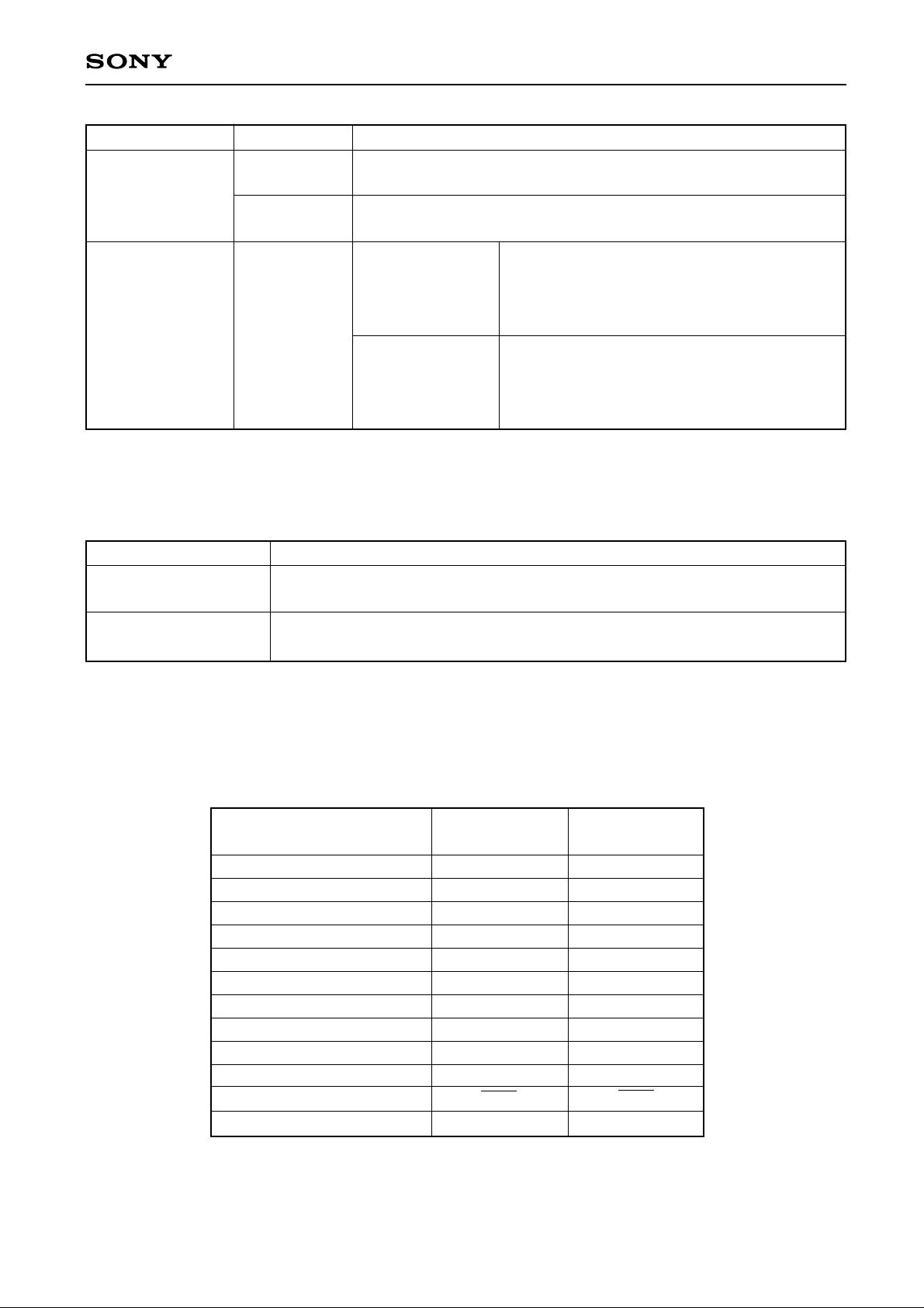
In the Digital CLV servo mode with DCLV ON-OFF set to 1, the sampling frequency of the internal digital filter
is switched at the same time as the switching between CLVP and CLVS.
Therefore, for CLVS, the cut-off frequency fC is 70 Hz when TB is set to 0, and 140Hz when TB is set to 1.
Command bit
DSPB=0
DSPB=1
Normal-speed playback. ECC quadruple error correction is made. Vari-pitch
control is enabled.
Double-speed playback. ECC double error correction is made. Vari-pitch control
is disabled.
Processing
Set FLFC at 1 when in double-speed playback mode (exclude the low power consumption special playback
mode). However, FLFC can be set to 0 during PLL pull-in (lock). Set to 0 for all other modes.
SENS Output
Microcomputer serial register
values (Latching unnecessary)
$0X
$1X
$2X
$3X
$4X
$5X
$6X
$AX
$BX
$CX
$EX
$7X, 8X, 9X, DX, FX
ASEQ=0
Z
Z
Z
Z
Z
Z
Z
GFS
COMP
COUT
OV64
Z
ASEQ=1
SEIN (FZC)
SEIN (A, S)
SEIN (T. Z. C)
SEIN (SSTOP)
XBUSY
FOK
SEIN (Z)
GFS
COMP
COUT
OV64
0
—15—
Page 16
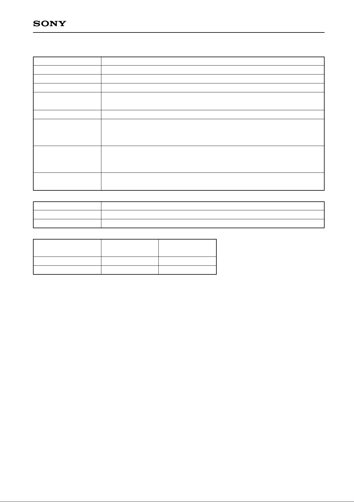
Description of SENS signals
CXD2500BQ
SENS output
Z
SEIN
XBUSY
FOK
GFS
COMP
COUT
OV64
Command bit
DPLL=0
DPLL=1
Meaning
SENS is at High-Z state.
SEIN signal, which was input to the CXD2500B, is output from SSP.
“L” when auto sequencer is in operation; “H” when terminated.
Output of the signal (normally FOK input from RF) input to the FOK pin. “H” when
Focus OK is received.
“H” when regenerated Frame Sync is obtained at the correct time.
Used in counting the number of tracks set in register B. “H” when the count is
latched to register B twice in succession. It is reset to “L” level when the count of
CNIN inputs equals the originally set number for register B.
Used in counting the number of tracks set in register B. “H” when the count is
latched to register B, then to register C. It is toggled every time the count of CNIN
inputs reaches the value set in register B.
“L” when after passing through the sync detection filter, the EFM signal become
longer than the 64 channel clocks.
Meaning
RFPLL enters analog mode. PDO, VCOI, and VCOO are used.
RFPLL enters digital mode. PDO becomes Z.
Command bit
BiliGL SUB=0
BiliGL SUB=1
BiliGL
MAIN=0
STEREO
SUB
BiliGL
MAIN=1
MAIN
Mute
Definition of Bilingual MAIN, SUB, and STEREO
MAIN; The input L-ch signal is output to both L-ch and R-ch.
Sub: The input R-ch signal is output to both L-ch and R-ch.
STEREO: The input L-ch and R-ch signals are output to both L-ch and R-ch respectively.
—16—
Page 17
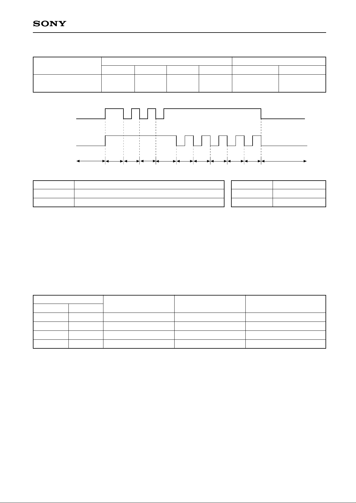
$AX Command
CXD2500BQ
Command
Audio CTRL
Vari UP
Vari DWN
Pitch
Command bit
Mute=0
Mute=1
D3 D2 D1 D0
Vari Vari
UP DWN
XTal 0% VCO 0% +0.1% +0.2% +0.3% +0.2% +0.1% +0% -0.1% -0.2% XTal 0%
Meaning
Muting is off unless condition to make muting occurs.
Muting is on. Peak register reset.
Data 1
Mute ATT
Command bit
Condition for Muting
(1) Mute=1 in register A
(2) Pin Mute=1
(3) D.OUT Mute F=1 in register 8 with D.Out ON (MD2=1)
(4) Elapse of over 35 msec after GFS turns “Low”
(5) BiliGL MAIN=Sub=1 in register 9
(6) PCT1=1 and PCT2=2 in register A
In the case of (1) to (4), zero-cross muting not exceeding 1 msec is performed.
Command bit
PCT1 PCT2
00
01
10
11
Meaning
Normal mode
Level meter mode
Peak meter mode
Normal mode
PCM Gain
×0 dB
×0 dB
Mute
×0 dB
Data 2
D3 D2
PCT1 PCT2
Meaning
ATT=0
ATT=1
Attenuation is off.
–12dB
ECC correction capacity
C1: Double, C2: Quadruple
C1: Double, C2: Quadruple
C1: Double, C2: Double
C1: Double, C2: Double
Level Meter Mode (See Timing Chart 1-4.)
• This mode makes the digital level meter function available.
• Inputting 96-bit clock pulses to SQCK will enable 96 data to be output to SQSO. Of the output data, the first
80 bits comprise Sub-Q data, which transmit the description for the data format to the Sub Code interface.
The last 16 bits are ordered LSB-first, of which the first 15 bits constitute PCM data (absolute value). The
final 1 bit is “High” if the prior PCM data was generated at the left channel; “Low” if generated at the right
channel.
• The PCM data is reset once it is read, and the L/R flag is reversed. While this state is kept until the next
read operation is started, testing for the maximum value is conducted.
—17—
Page 18
CXD2500BQ
Peak Meter Mode (See Timing Chart 1-5.)
• In this mode, the maximum value of PCM data is detected whether the channel involved is L-ch or R-ch.
To read the detected maximum value, it is necessary to input 96 clock pulses to SQCK.
• When 96 clock pulses have been input to SQCK, 96 bits of data is output to SQSO. At the same time, the
data is re-set in an internal register of the LSI.
That is, the PCM peak detection register is not reset when it is read.
• To reset the PCM peak register, set both PCT1 and PCT2 to 0. Or, Set $AX mute.
• In this mode, the absolute time of Subcode Q is controlled automatical.
• Namely, every time a peak value is detected, the absolute time when the CRC was passed is stored. The
program time operation is performed in the normal way.
• The last bit (L/R flag) of the 96-bit data stays 0.
• In this mode, the preceding value holding and average value interpolation data are fixed to level (–∞).
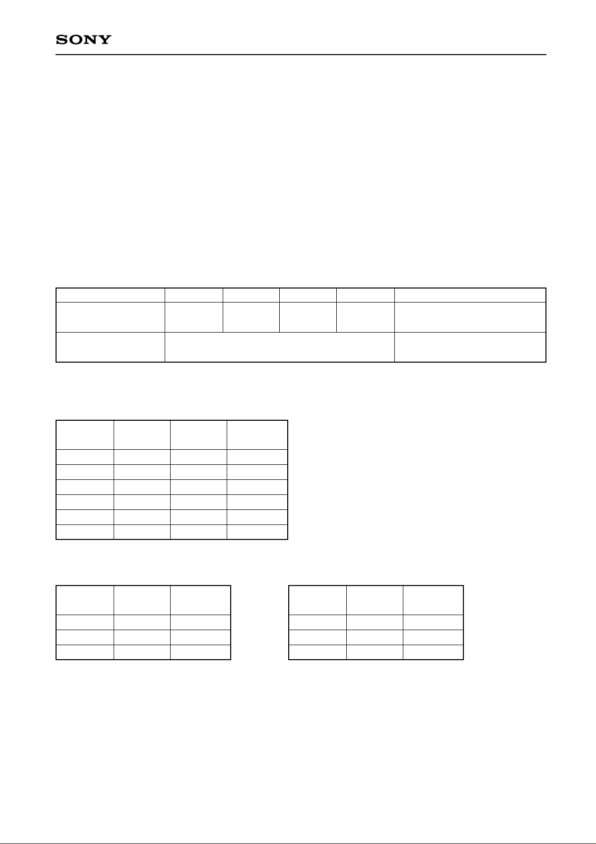
$CS Command
Command
Servo factor setting
CLV CTRL ($DX)
D3 D2 D1 D0
Gain Gain Gain Gain
MDP1 MDP0 MDS1 MDS0
Gain
CLVS
Explanation
Only DCLV=1 is effective.
DCLV=1 and DCLV=0 are both
effective.
This command is used to externally set the spindle servo gain when DCLV=1.
• Gain setting for CLVS mode: GCLVS
Gain Gain Gain GCLVS
MDS1 MDS0 CLVS
0 0 0 –12dB
0 0 1 –6dB
0 1 0 –6dB
0110dB
Note: When DCLV=0, the CLVS gain is
determined as follows:
If Gain CLVS=0, then GCLVS=–12 dB.
If Gain CLVS=1, then GCLVS=0 dB
1000dB
1 0 1 +6dB
• Gain setting for CLVP mode: GMDP, GMDS
Gain Gain GMDP
MDP1 MDP0
0 0 –6 dB
0 1 0 dB
1 0 + 6dB
Gain Gain GMDS
MDS1 MDS0
0 0 –6dB
0 1 0dB
1 0 +6dB
—18—
Page 19
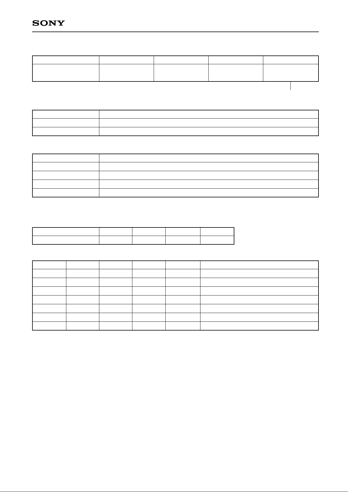
$DC Command
CXD2500BQ
Command
CLV CTRL
D3
DCLV
PWM MD
Command bit
DCLV PWM MD=1
DCLV PWM MD=0
Specification of PWM mode for digital CLV. Both MDS and MDP are used.
Specification of PWM mode for digital CLV. Ternary MDP values are output.
Command bit
TB=0
TB=1
TP=0
TP=1
In CLVS or CLVH mode, bottom value is held at periods of RFCK/32.
In CLVS or CLVH mode, bottom value is held at periods of RFCK/16.
In CLVS mode, peak value is held at periods of RFCK/4.
In CLVS mode, peak value is held at periods of RFCK/2.
In CLVH mode, peak holding is made at 34 kHz.
$EX Command
Command
CLV mode
D3 D2 D1 D0
CM3 CM2 CM1 CM0
D2
TB
D1
TP
Description (See Timing Chart 1-6.)
Description
D0
CLVS
Gain
See “$CX Command.”
CM3 CM2 CM1 CM0 Mode
0 0 0 0 STOP
1 0 0 0 KICK
1 0 1 0 BRAKE
See Timing Chart 1-7.
See Timing Chart 1-8.
See Timing Chart 1-9.
Explanation
1 1 1 0 CLVS
1 1 0 0 CLVH
1 1 1 1 CLVP
0 1 1 0 CLVA
STOP: Spindle motor stop mode
KICK: Spindle motor forward run mode
BRAKE: Spindle motor reverse run mode
CLVS: Rough servo mode for use for pulling disc run into RF-PLL capture range when the RF-PLL circuit
lock has been disengaged
CLVP: PLL servo mode
CLVA: Automatic switching mode for CLVS and CLVS. This mode is used during normal play status.
—19—
Page 20
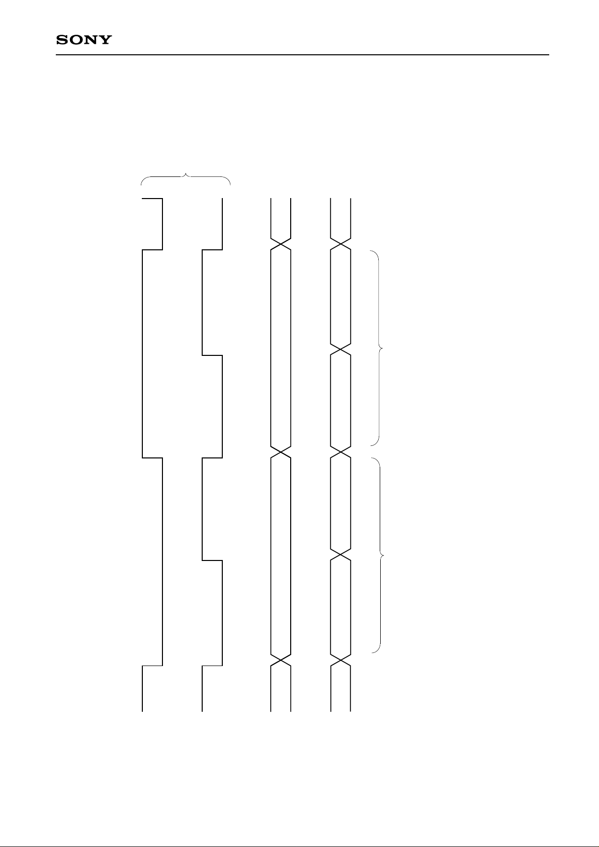
CXD2500BQ
48bit Slot
If C2 pointer=1,
data is NG
Timing Chart 1-3
LRCK
WDCK
Rch 16bit C2 Pointer Lch 16bit C2 Pointer
C2PO
CDROM=0
—20—
Rch C2 pointer Lch C2 pointer
C2 Pointer for upper 8bit C2 Pointer for Lower 8bit C2 Pointer for upper 8bit C2 Pointer for Lower 8bit
C2PO
CDROM=1
Page 21
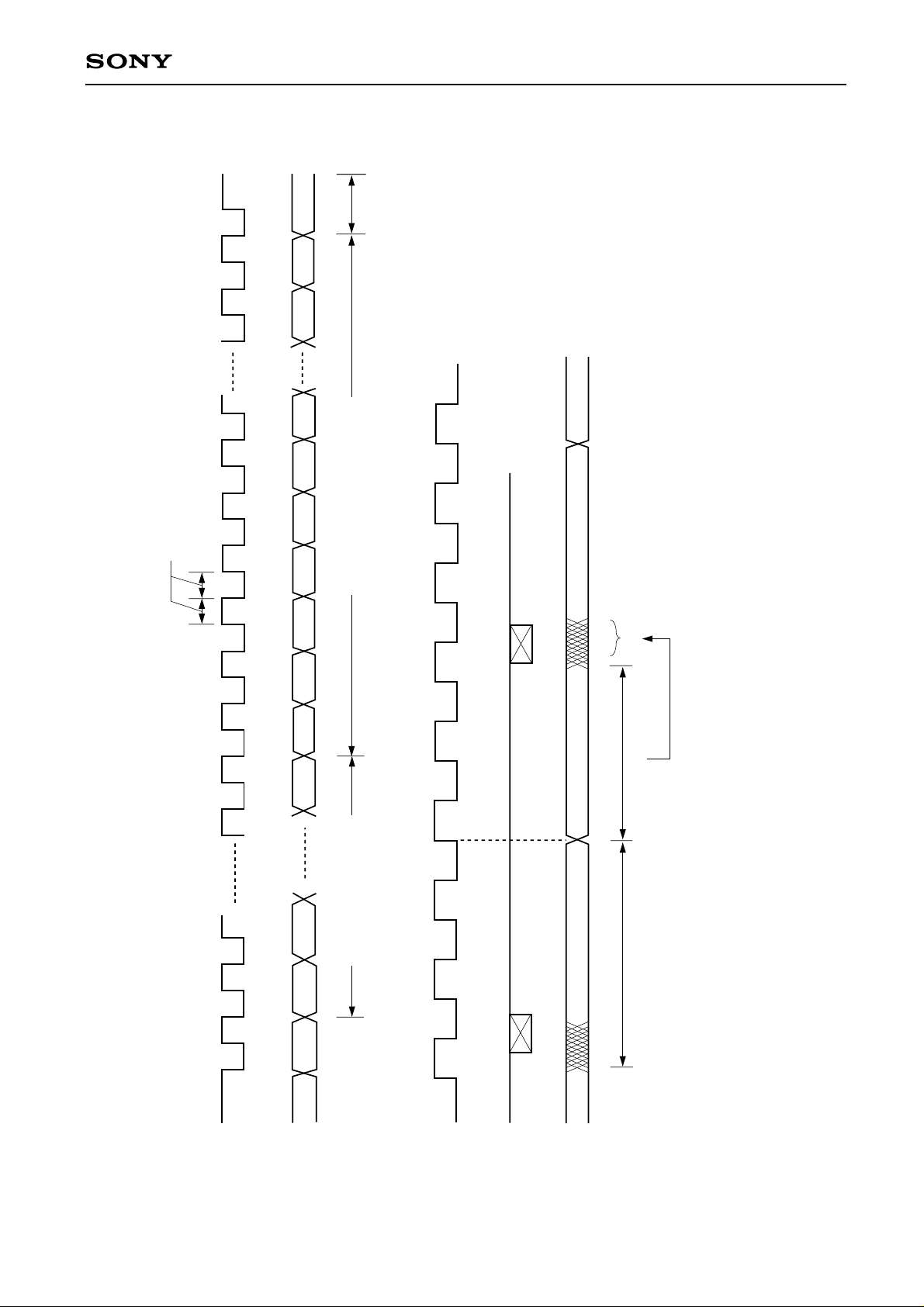
CXD2500BQ
L/RD14D13D6D5D4D3D2D1D0
96
750ns to 120µs
L/R flag
Peak data
23
15-bit peak-data
Absolute value display, LSB first
1
16 bit
8180123
Sub-Q Data
CRCF
SQCK
SQSO
23
See "Sub Code interface"
1
WFCK
96 clock pulses 96 clock pulses
SQCK
L/R CRCF R/L CRCF
SQSO
Level Meter Timing
Peak data of this section
96 bit data
Hold section
Timing Chart 1-4
—21—
Page 22
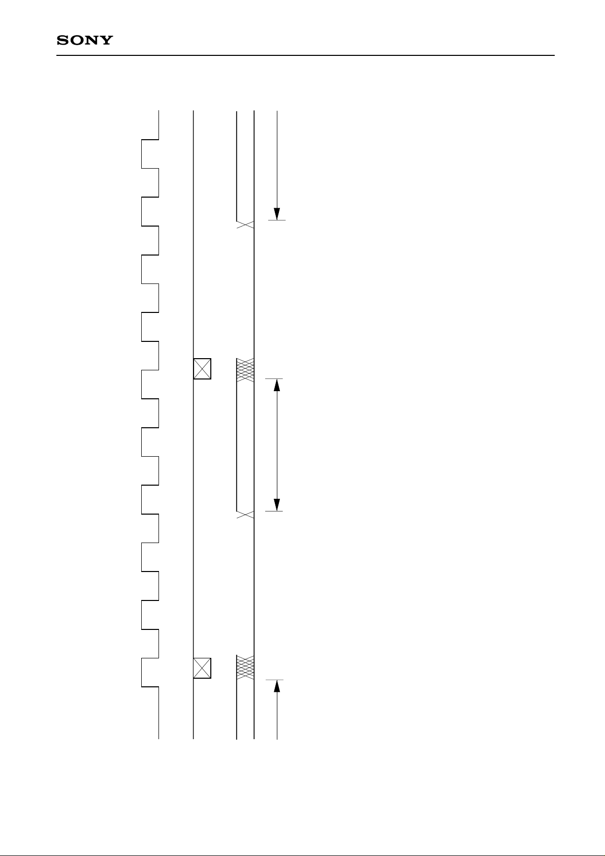
CRCF
CXD2500BQ
Measurement
96 clock pulses
CRCF
Measurement
123 123
Peak Meter Timing
Timing Chart 1-5
WFCK
96 clock pulses
CRCF
Measurement
SQCK
—22—
Page 23
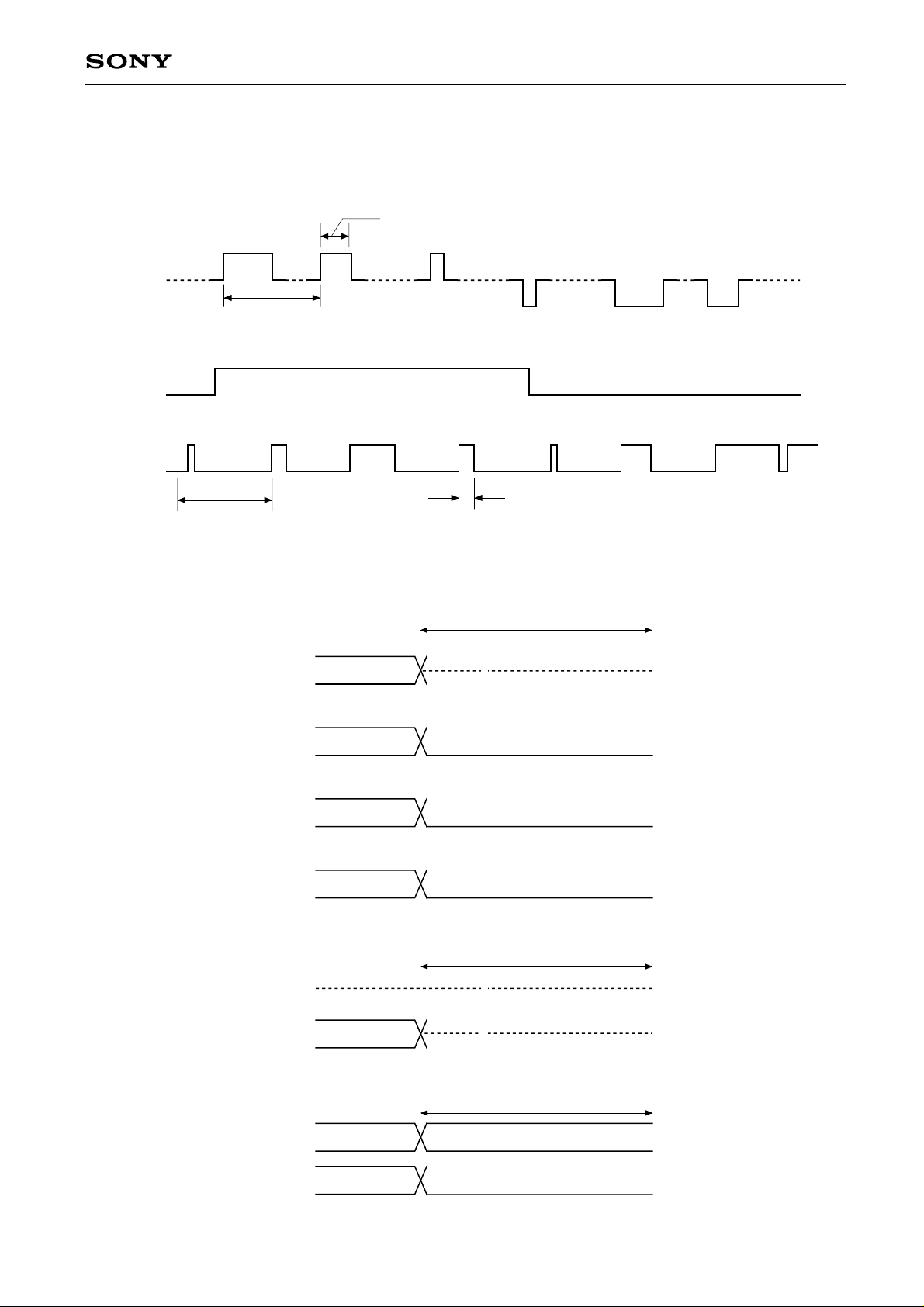
Timing Chart 1-6
DCLV PWM MD=0
MDS
CXD2500BQ
Z
n·236 (nsec) n=0 to 31
Acceleration
MDP
DCLV PWM MD=1
MDS
MDP
Timing Chart 1-7
7.6µSec
132KHz
7.6µSec
MDS
Acceleration
Output Waveforms with DCLV=1
DCLV=0
Z
Z
Deceleration
Deceleration
n·236 (nsec) n=0~31
STOP
MDP
FSW
MON
DCLV=1 DCLV PWM MD=0
MDS
MDP
DCLV=1 DCLV PWM MD=1
MDS
MDP
L
L
L
STOP
Z
Z
STOP
L
FSW and MON are the same as for DCLV=0
—23—
Page 24
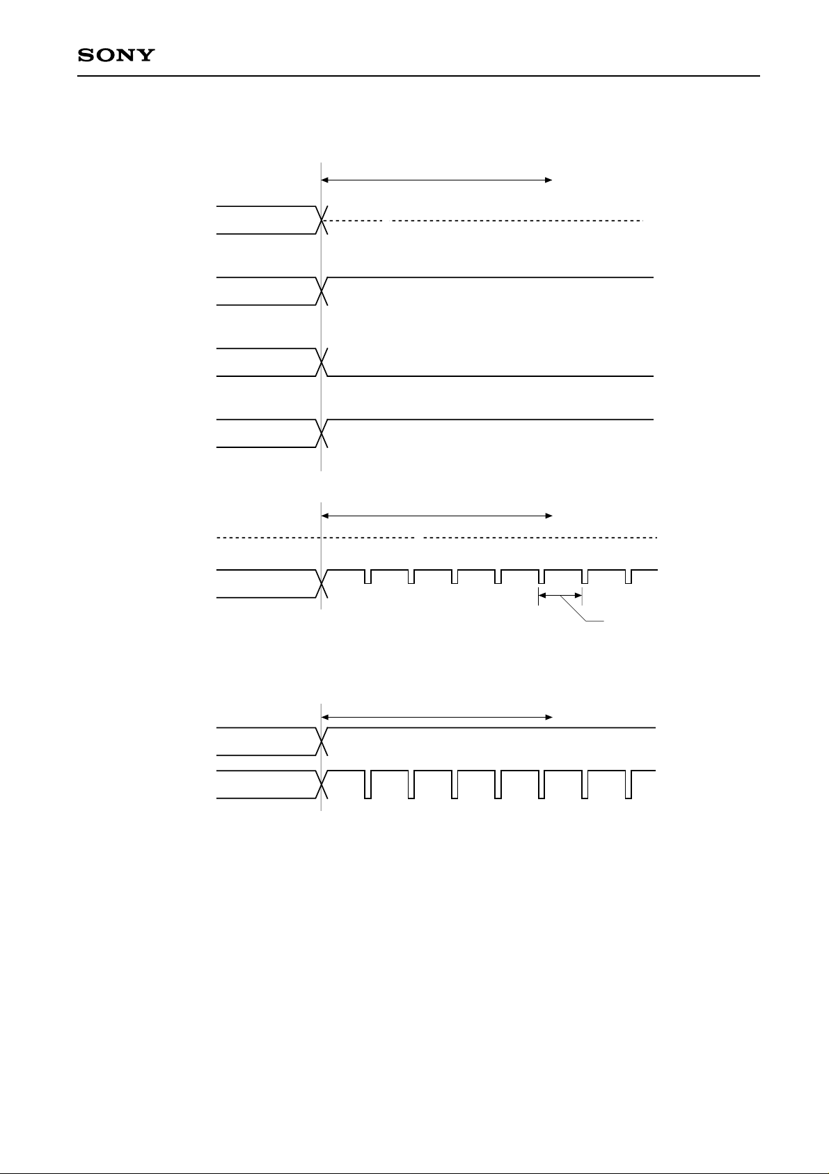
Timing Chart 1-8
CXD2500BQ
KICK
DCLV=0
MDS
MDP
FSW
MON
DCLV=1 DCLV PWM MD=0
MDS
MDP
Z
H
L
H
KICK
Z
H
Z
7.6µs
DCLV=1 DCLV PWM MD=1
MDS
MDP
FSW and MON are the same as for DCLV=0
KICK
H
H
L
FSW and MON are the same as for DCLV=0
—24—
Page 25
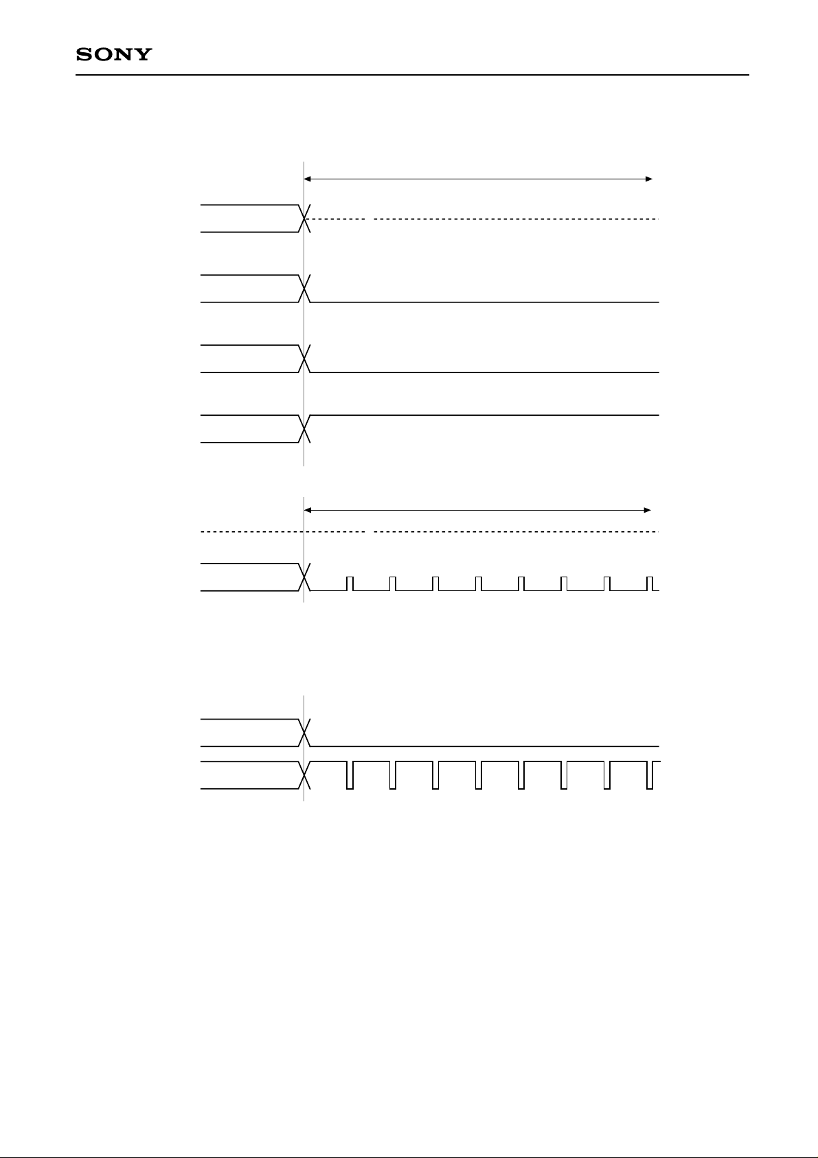
Timing Chart 1-9
CXD2500BQ
BRAKE
DCLV=0
MDS
MDP
FSW
MON
DCLV=1 DCLV PWM MD=0
MDS
MDP
Z
L
L
H
BRAKE
Z
L
Z
DCLV=1 DCLV PWM MD=1
MDS
MDP
FSW and MON are the same as for DCLV=0
FSW and MON are the same as for DCLV=0
—25—
Page 26

CXD2500BQ
§2 Subcode Interface
In this section, the subcode interface will be explained.
The contents of the subcode interface can be externally read in two ways. The subcodes P through W totaling
8 bits can be read from SBSO by inputting EXCK to the CXD2500B.
Sub-Q can be read after conducting a CRC check on the 80bits of information in the subcode frame. First,
check SCOR and CRCF, then input 80 clock pulses to SQCK and read the data.
§2-1 P-W Subcode Read
These subcodes can be read by entering EXCK immediately after the fall of WFCK. (See Timing Chart 2-1.)
§2-2 80-bit Sub-Q Read
Figure 2-2 shows a block diagram of the peripheral part of the 80-bit Sub-Q register.
• The Sub Q regenerated on a bit-per-frame basis is input to the 80-bit serial/parallel register and the CRC
circuit.
• When the results of CRC of the 96-bit Sub-Q are OK, CRCF is set to 1 and the 96-bit data is output to
SQSO.
Furthermore, it is loaded into the 80-bit, parallel/serial register.
If SQSO is “H” after the output of SCOR, it can be taken that CPU has been loaded a new set of CRCOK
data.
• When 80-bit data is loaded into CXD2500B, MSB and LSB are reversed within each byte of the data.
Therefore, the bits are ordered LSB-first within each byte, even though the byte arrangement is kept
unchanged.
• When 80 bits of data are confirmed to have been loaded, SQCK is input to read the data. Subsequently in
the CXD2500B, the input of SQCK is detected and the retriggerable monostable multivibrator is reset during
Low.
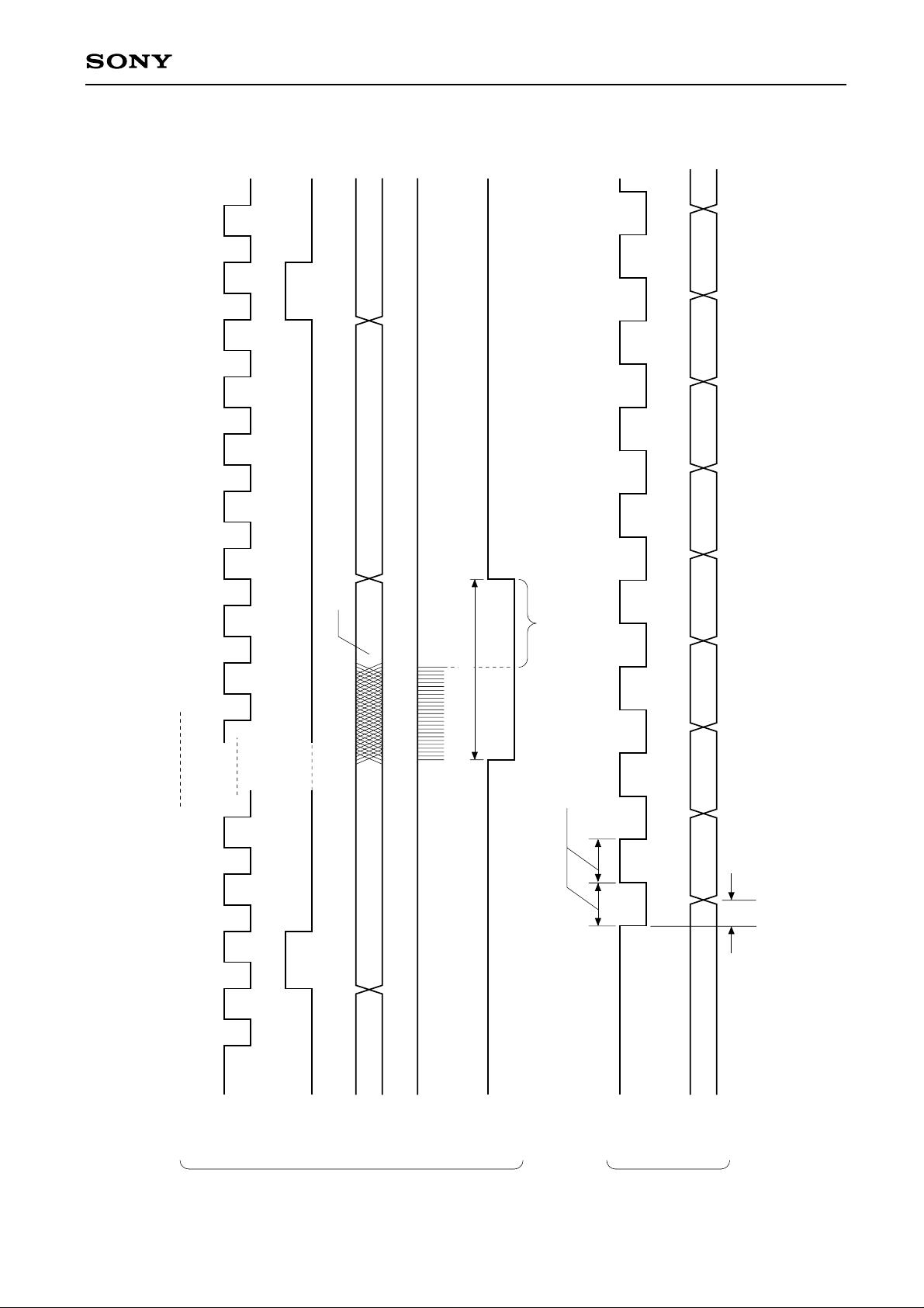
• The time constant of the retriggerable monostable multivibrator ranges from 270 to 400 µs. If the time of
High for SQCK is less than this time constant, the monostable multivibrator will keep resetting, preventing the
contents of the P/S register from being loaded into the P/S register.
• While the monostable multivibrator is resetting, data loading into the peak detection parallel/serial register
and 80-bit parallel/serial register is forbidden.
Therefore, while data read operation is carried out at clock periods shorter than the time constant of the
monostable multivibrator, the contents of these registers are retained without being rewritten by CRCOK, etc.
• The CXD2500B permits the peak detection register to be connected to the shift-in of the 80-bit P/S register.
For Ring Control 1, the input and output are short-circuited during peak meter and level meter mode.
For Ring Control 2, the input and output are short-circuited during peak meter mode only.
The Ring Controls are arranged in this way in order for the registers to be reset each time their contents are
read in the level meter mode, while preventing destructive read in the peak meter mode.
To enable this control, 96 clock pulses must be input to the peak meter mode.
• As afore mentioned, in the peak meter mode, the absolute time following the generation of a peak value is
stored.
These operations are shown in Time chart 2-3.
Note: To perform the above operations, the duration of the clock pulse input to SQCK must be between 750ns
and 120 µs for both “High” and “Low”.
—26—
Page 27
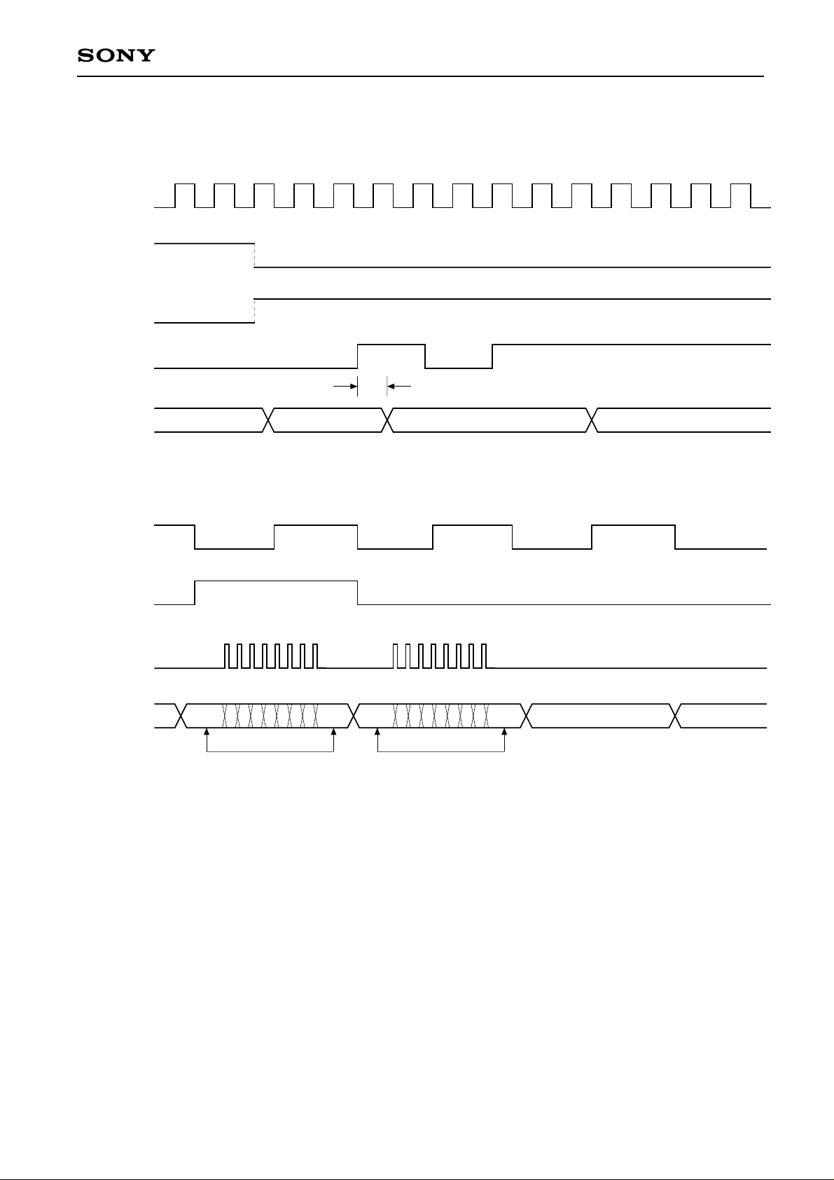
Timing Chart 2-1
Internal
PLL c lock
4.3218±∆MHz
WFCK
SCOR
EXCK
CXD2500BQ
750ns max
SBSO
WFCK
SCOR
EXCK
SBSO
S0·S1 Q R
S0·S1 Q R S T U V W P1S0·S1 Q R S T U V W P1
Same Same
Subcode P. Q. R. S. T. U. V. W Read Timing
P2 P3
—27—
Page 28
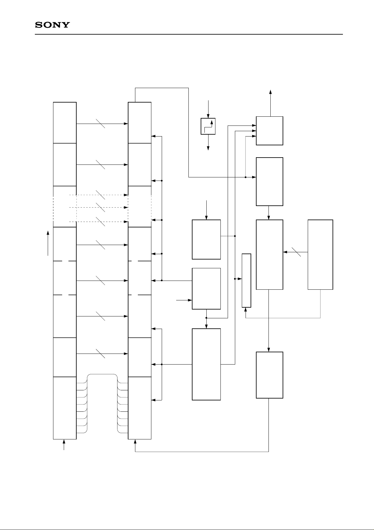
CXD2500BQ
SQSO
SO
8
SQCK
ADDRS CTRL
LD
8
LD
8888
LD
LD
8
80 bit S/P Register
8
LD
80 bit P/S Register
SUBQ
SHIFT
SHIFT
Monostable
multivibrator
CRCC
L OAD CONTROLE
CRCF
SI
LD
SO
Mix
Ring control 2
16
16 bit P/S register
Peak detection
(A MIN)
(ASEC)
H
G
E F
(A FRAM)
C D
A B
SIN
SUB-Q
Block Diagram 2-2
LD
Order
Inversion
8
LD
A
B
CD
LD
E
FG
H
SI
for peak value
ABS time load control
Ring control 1
—28—
Page 29
CRCF 2
CXD2500BQ
CTL3
CTL2
CTL1
91 92 93 94 95 96 97 98
1 2 3
CTL0
CRCF 1
Determined by mode
When SQCK=High, 270 to 400µsec
1 2 3
Register load forbidder
80 or 96 Clock
750ns to 120µs
Inversion
Order
CRCF 1
ADR3
ADR2
ADR1
ADR0
300ns max
Timing Chart 2-3
WFCK
SCOR
SQSO
SQCK
—29—
(Internal)
Monostable
multivibrator
SQCK
CRCF
SQSO
Page 30

CXD2500BQ
§3 Other Functions
§3-1 Channel Clock Regeneration Using Digital PLL Circuit
• Demodulation of regenerated EFM signals using an optical system requires the use of channel clock pulses.
The EFM signal to be demodulated has been modulated into an integer multiple of the channel clock period
T, ranging from 3T to 11T.
To read the information conveyed by the EFM signal, it is essential to correctly recognize the integral value;
hence, the need to use channel clock pulses.
In an actual CD player, the pulse width of the EFM signal will vary, affected by fluctuations of the disc
rotation. For this reason, it is necessary to use a PLL in regenerating channel clock pulses.
Figure 3-1 shows a block diagram of the 3-stage PLL contained in the CXD2500B.
• The 1st-stage PLL is used for vari-pitch regeneration. To use this PLL, LPF and VCO are necessary as
external parts.
The minimum pitch variable possible is 0.1 %. The output of this 1st-stage PLL is used as the standard for
all the clock pulses used in the LSI.
When vari-pitch control is not in uses, connect the output pin of XTAO to VCKI.
• The 2nd-stage PLL generates high frequency clock pulses necessary for the 3rd-stage digital PLL.
• The 3rd-stage comprises a digital PLL used to regenerate the actual channel clock pulses. It realizes a
capture range of ±150 kHz (normal conditions) or more.
• The digital PLL features a secondary loop. It is controlled through the primary loop (phase) secondary loop
(frequency).
When FLFC=1, the secondary loop can be turned off.
• When high frequency components such as 3T, 4T, are deviated, turning off the secondary loop will provide
better play ability.
• However, the capture range will be 50 kHz.
—30—
Page 31
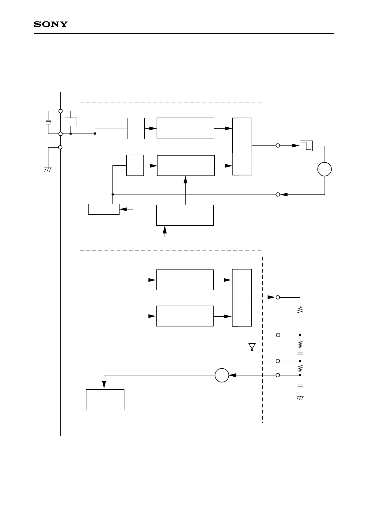
Block Diagram 3-1
CXD2500BQ
X'Tal
XTSL
OSC
16,9344MHz
(384Fs)
2/1 MUX
1/4
1/4
Vari-pitch
1/1000
1/1000+n
Up down counter
n=-217 to 168
Microcomputer control Vari-pitch
I/M
Phase comparator
VPCO
19. 78 to 13.26MHz
PCO
LPF
VCKI
VCO
Digital PLL
D2500B
I/N
—31—
RFPLL
VCO
Phase comparator
FILI
FILO
CLTV
Page 32
CXD2500BQ
§3-2 Frame Sync Protection
• During CD player operation at normal speed, Frame Sync is recorded approximately once every 136 µs (at
7.35 kHz).
This signal can be used to identify the data within each frame. When Frame Sync cannot be recognized, the
data also cannot be identified; as a result, it is treated as an error. Therefore, correct Frame Sync
recognition is very important to ensure high play ability for the CD player.
• The CXD2500B employs window protection, front protection and rear protection to realize a powerful Frame
Sync protection. The CXD2500B offers two window widths, one for use when the player is subjected to
rotational disturbance and the other for use without such disturbance (WSEL=0/1).
The front protection counter is fixed at 13 and the rear protection counter at 3. Therefore, during normal play
back, when the frame sync cannot be detected due to damages on the disc. If the number to frames with
undetected Frame Sync exceeds 13, the window is released and the Frame Sync signal are re-synchronized.
If no Frame Sync is correctly detected in 3 successive frames immediately after Frame Sync resynchronization performed following a window release, the window is released at once.
§3-3 Error Correction
• On CDs, each data unit (8 bits) is formatted so that it is contained in two correction codes, C1 and C2. C1
consists of 28 bytes of information and 4-byte parity, whereas C2 is made up of 24 bytes of information and
4-byte parity. Both C1 and C2 comprise a read Solomon code with a minimum distance of 5.
• C1 realizes double corrections and C2 realizes quadruple corrections, both by the refined superstrategy
method.
• To prevent erroneous C2 corrections, C1 pointer based on the conditions of C1 error, EFM signal play back,
and player operation during C1 operation is attached to the corrected data.
• The status of error correction can be monitored from outside the LSI. It is indicated as shown in Table 3-2.
• When C2 pointer is High, this signifies uncorrectable data error. The data are either previous data held
subsitute the error, or an average value interpolation.
MNT3 MNT2 MNT1 MNT0
0000
0001
0010
0011
0100
0101
0110
0111
1000
1001
1010
1011
1100
1101
1110
1111
Table 3-2 Indication of error correction status
Description
C1: No error detected. C1 pointer reset.
C1: 1 error corrected. C1 pointer set.
—
—
C1: No error detected. C1 pointer set.
C1: 1 error corrected. C1 pointer set.
C1: 2 errors corrected. C1 pointer set.
C1: Uncorrectable error. C1 pointer set.
C2: No error detected. C2 pointer reset.
C2: 1 error corrected. C2 pointer reset.
C2: 2 errors corrected. C2 pointer reset.
C2: 3 errors corrected. C2 pointer reset.
C2: 4 errors corrected. C2 pointer reset.
—
C2: Uncorrectable error. C1 pointer copied.
C2: Uncorrectable error. C2 pointer set.
—32—
Page 33
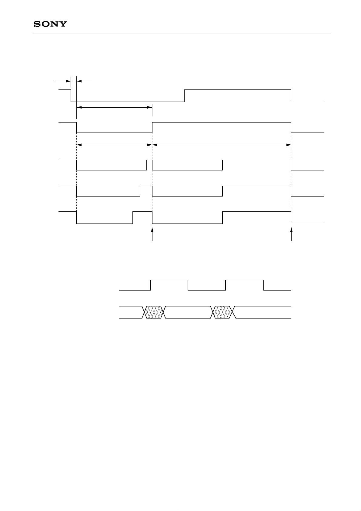
Timing Chart 3-3
Normal - speed PB
RFCK
MNT3
CXD2500BQ
400 to 500nsec
t=Dependent on error
condition
MNT2
MNT1
MNT0
C1 co rrectio n
C4M
MNT0 to 3
Strobe
Valid
C2 co rrectio n
Strobe
Valid
Invalid
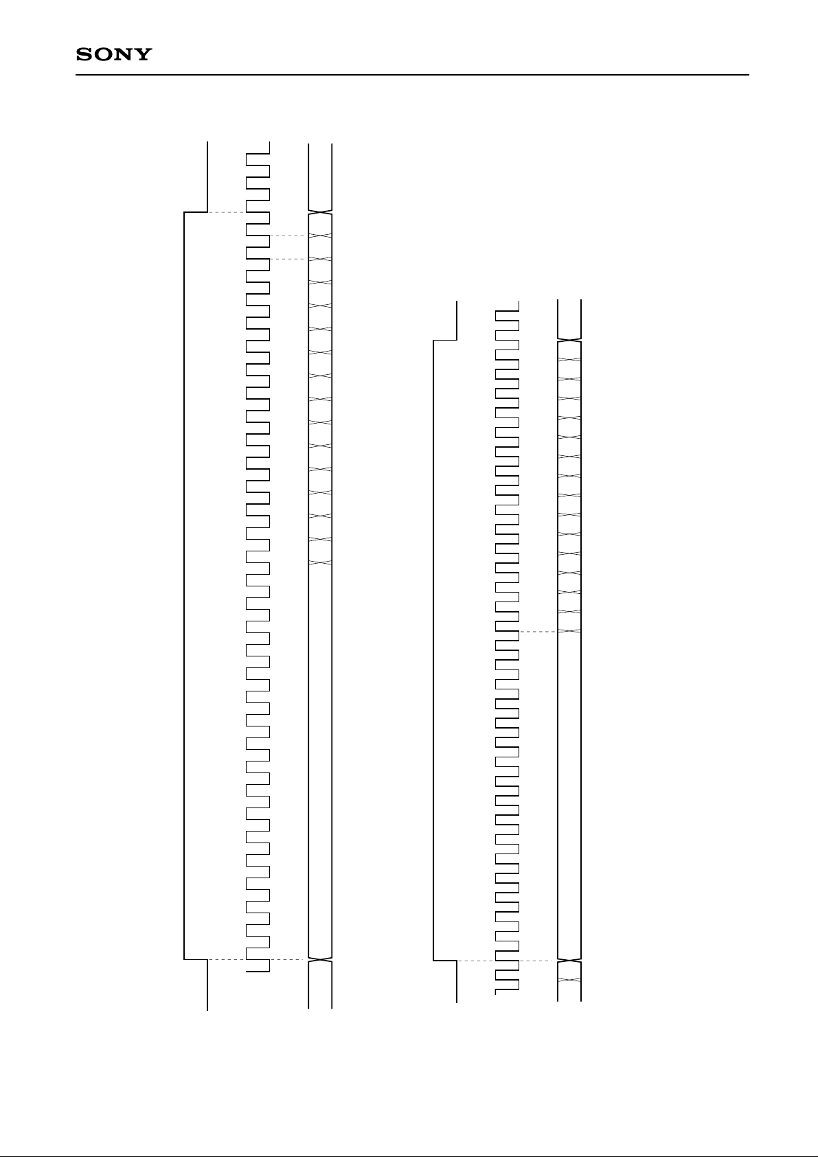
§3-4 DA Interface
• The CXD2500B has two modes of DA interface.
a) 48-bit slot interface
This is an MSB-first interface made up of LRCK signals with 48-bit clock cycles per LRCK cycle. While
the LRCK signal is High, the data going through this interface is of the left channel.
b) 64-bit slot interface
This is an LSB-first interface made up of LRCK signals with 64-bit clock cycles per LRCK cycle. While
the LRCK signal is Low, the data going through this interface is of the left channel.
—33—
Page 34
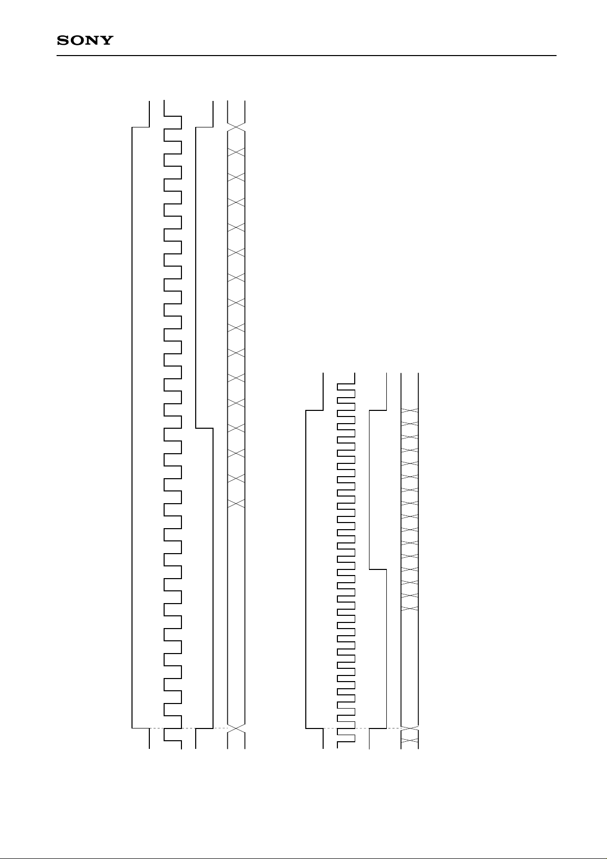
24
CXD2500BQ
RMSB
L10 L9 L8 L7 L6 L5 L0L1L2L3L4
L ch MSB (15) L14 L13 L12 L11
R ch MSB
0
L
48 bit slot Normal-Speed Playback PSSL=L
Timing Chart 3-4
LRCK
(44.1K)
123456789101112
DA15
(2.12M)
WDCK
R0
DA16
WDCK
L ch MSB (15)R0
DA16
12 24
48 bit slot Double-Speed Playback
DA15
LRCK
(88.2K)
(4.23M)
—34—
Page 35
30 31 32
CXD2500BQ
L ch LSB (0)
R15
12 13 14
20
10 11
L ch LSB
30 31 32
12 13 14 15
10 11
25
1 2 3 4 5 6 7 8 9
20
1 2 3 4 5 6 7 8 9
15
64 Bit slot Normal Speed PB PSSL=L
Timing Chart 3-5
DA 12
(44.4K)
10
1 2 3 4 5 6 7 8 9 11 12 13 14 15
DA 13
(2.82M)
R ch LSB (0)
DA 14
10
1 2 3 4 5
64 Bit slot Double–Speed PB
DA 12
(88.2K)
DA 13
—35—
(5.64M)
R ch LSB (0)
15
L
DA 14
Page 36
CXD2500BQ
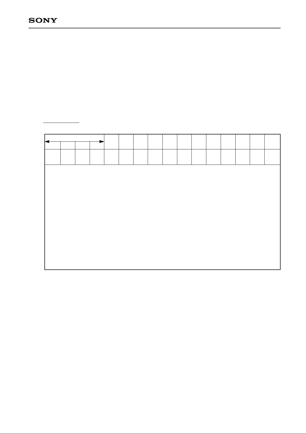
§3-5 Digital Out
There are three digital-out formats: type 1 for use at broadcasting stations, type 2, form 1 for use in general
civil applications, and type 2, form 2 for use in software production. The CXD2500B supports type 2, form 1.
The clock accuracy for the channel status is automatically set at Level II when the X'tal clock is used, or
Level III when vari-pitch control is made.
CRC checks are conducted on the Sub-Q data on the first 4 bits (bits 0-3). The data is input only after two
checks are passed in succession.
The X'tal clock is set to 34 MHz, and variable pitch is reset. When D out is output at DSPB=1, set MD2 to 0
and turn off D out 34.
Digital Out C bit
0123456 789101112131415
0
16
32
48
176
From sub-Q
ID0 ID1 COPYEmph
000010000000
00000000000000/100
0
Bits 0-3: Sub-Q control bits required to pass the CRC twice in succession.
bit 29: Varipitch: 1 X'tal: 0
Table 3-6 Digital Out C bits
§3-6 Servo Auto Sequencer
The servo auto sequencer controls a series of operation including auto-focusing and track jumping. When an
auto sequence command is received from CPU, the servo auto sequencer automatically executes autofocusing, 1-track jumping, 2N track jumping and M track moving.
During auto sequence execution (X Busy=Low), as SSP (servo signal processing LSI) is used exclusively,
commands from CPU are not transferred to SSP. Instead, the commands can be sent to CXD2500B.
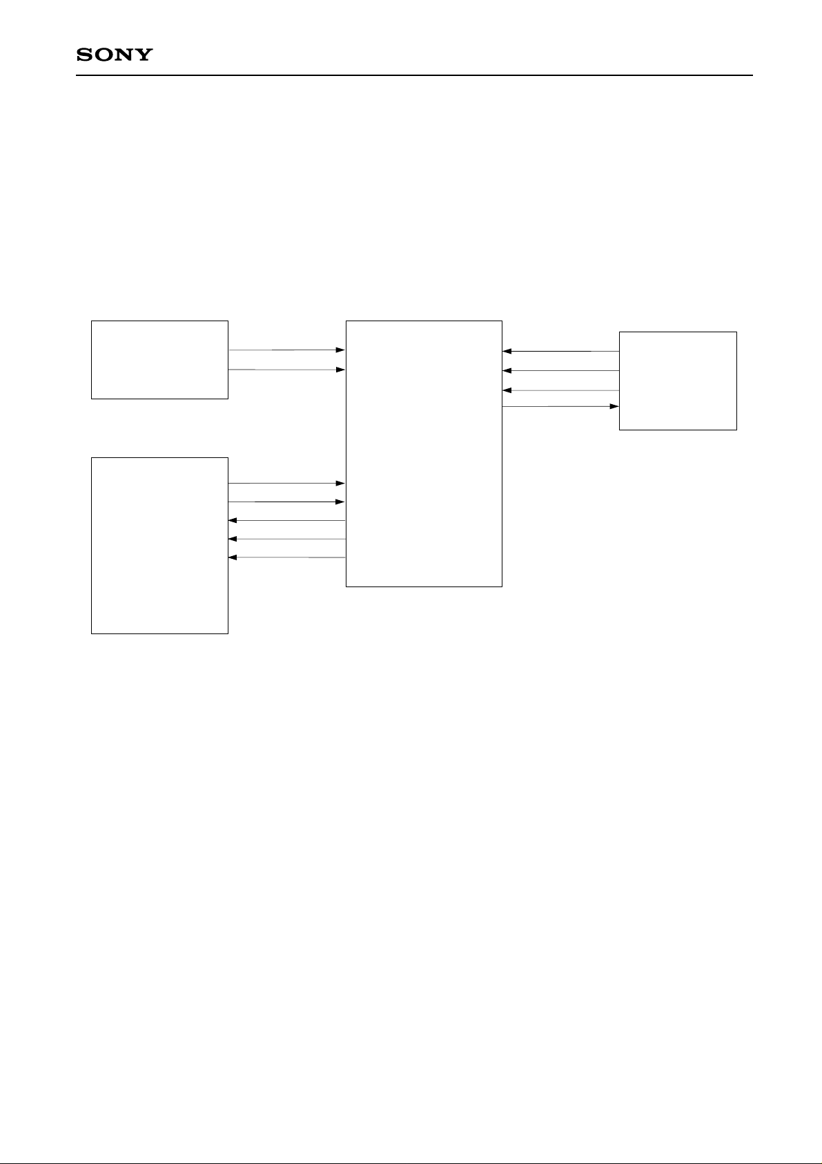
To make this servo auto sequencer usable, connect a CPU, RF and SSP to the CXD2500B as shown in
Figure 3-7 and set A.SEQ ON-OFF of Register 9 to ON.
When the CLOK changes from Low to High while XBUSY is at Low, from that point on to a maximum of 100
µsec, X BUSY does not become High.
Due to the monostable multivibrator which is reset when CLOK is Low (XBUSY=Low), transfer of erroneous
data to SSP is prevented when XBUSY changes from Low to High.
—36—
Page 37
(a) Auto Focus ($47)
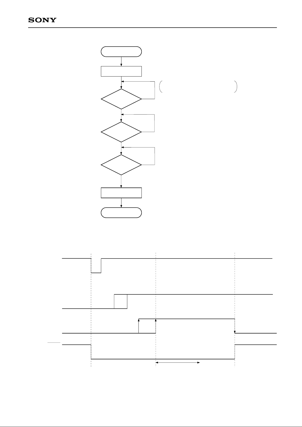
In auto focus operation, ‘focus search up’ is performed, FOK and FZC are checked, and the focus servo
is turned on. When $47 is received from CPU, the focus servo is turned on through the steps shown in
Figure 3-8. Since this auto focus sequence begins with ‘focus search up,’ it requires the pickup to be
put down (focus search down) beforehand.
Blind E of Register 5 is used to eliminate chattering from FZC. The focus servo is turned on at the
trailing edge of FZC after staying High continuously for a longer period than E.
System Configuration for Auto Sequencer Operation (Example)
CXD2500BQ
RF
SSP
MIRR
FOK
C.out
SENS
DATA
CLK
XLT
MIRR
FOK
CNIN
SEIN
DATO
CLKO
XLTO
CXD2500B
Figure 3-7
DATA
CLOK
XLAT
SENS
Micro-computer
—37—
Page 38
Auto focus
Focus search up
Checking whether FZC has stayed High
longer than time E set in Register 5.
CXD2500BQ
FOK=H
YES
FZC=H
YES
FZC=L
YES
Focus servo ON
END
NO
NO
NO
Figure 3-8 (a) Flow chart of auto focus operation
XLAT
FOK
SEIN(FZC)
BUSY
Command to SSP
$47 latch
$03
Blind E
Figure 3-8 (b) Timing chart for auto focus operation
$08
—38—
Page 39

(b) Track Jump
Track jump operation includes 1, 10 and 2N track jumps. Do not perform this track jump unless the focus,
tracking and sled servos are on. Such steps as tracking gain up and braking are not included in this track
jump. Therefore, the commands for tracking gain up and brake ON ($17) must be issued in advance.
• 1-track jump
When a $48 is received from CPU (or a $49 from REV), the servo auto sequencer executes a FWD
(REV) 1-track jump as shown Figure 3-9. The values of blind A and brake B must be set in Register 5.
• 10-track jump
When a $4H is received from CPU (or a $4B from REV), the servo auto sequencer executes a FWD
(REV) 10-track jump as shown in Figure 3-10. The principal difference between the 1-track and 10-track
jumps is whether the sled is kicked or not. In the 10-track jump, the actuator after being kicked is braked
when CNIN has been counted 5 tracks. When the actuator has adequately slowed down as a result of
braking, the tracking and sled servos are turned on (this actuator slow-down is detected by checking
whether the CNIN period has exceeded overflow C specified in Register 5).
• 2N track jump
When a $4C is received from CPU (or a $4D from REV), the servo auto sequencer executes a FWD
(REV) 2N track jump. The number of tracks to be jumped is determined by N, set Register 7 beforehand.
The maximum permissible number is 216. In actual use, however, it is subject to limitation imposed by the
actuator.
When N is smaller than 16, the jumps are counted by means of counting CNIN signals. If N is 16 and
above, MIRR signals are counted instead of CNIN signals.
The 2N track jump sequence is basically the same as the 10-track jump sequence. The only difference
between them is that, in the 2N track jump sequence, the sled is kept moving for time D specified in
Register 6 after the tracking servo is turned on.
CXD2500BQ
• M track move
When a $4E is received from CPU (or a $4F from REV), the servo auto sequencer executes a FWD
(REV) M-track move as shown in Figure 3-12. The maximum value that can be set from M is 216. The
track moves are counted in the same way as for 2N track jumps. That is, when M is smaller than 16, the
moves are counted by means of counting CNIN signals. If M is 16 and above, MIRR signals are counted
instead of the CNIN signals. In this M track move, only the sled is moved. This method is suitable for a
large track move ranging from several thousand to several tens of thousand tracks.
—39—
Page 40
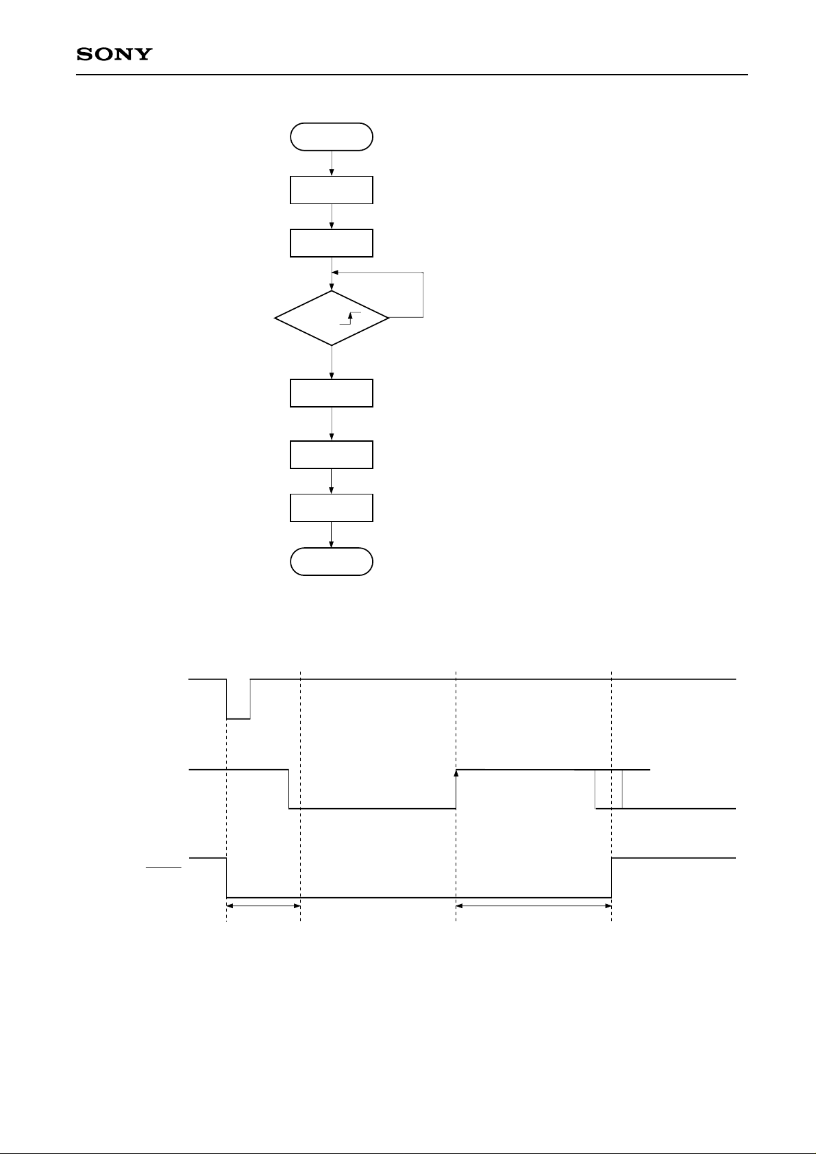
1 Track
CXD2500BQ
Track Kick
Sled servo
WAIT
(Blind A)
CNIN=
YES
Track REV
Kick
WAIT
(Brake B)
Track sled
Servo ON
END
(REV kick is made for REV jump.)
NO
(FWD kick is made for REV jump.)
XLAT
CNIN
BUSY
$48 (REV=$49) latch
Blind A
$28 ($2C)Commands to SSP
Figure 3-9 (a) Flow chart of 1-track jump
Brake B
$25$2C ($28)
Figure 3-9 (b) Timing chart for 1-track jump
—40—
Page 41
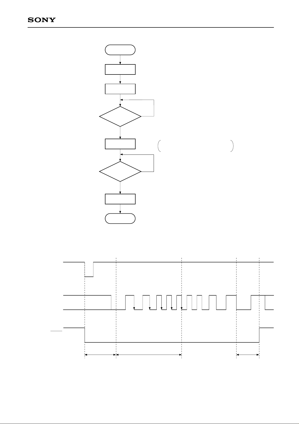
10 Track
Track, Sled
FWD Kick
WAIT
(Blind A)
CNIN=
5?
YES
CXD2500BQ
(5 CNINs are counted.)
NO
XLAT
C=Overflow?
Figure 3-10 (a) Flow chart of 10-track jump
$4A (REV=$4B) latch
Track, REV
FWD Kick
YES
Track, Sled
Servo ON
END
Checking whether the CNIN period has
exceeded the value of overflow C.
NO
CNIN
BUSY
Blind A CNIN 5count
$2A ($2F) $2E ($2B)
Figure 3-10 (b) Timing chart for 10-track jump
—41—
Overflow C
$25Commands to SSP
Page 42
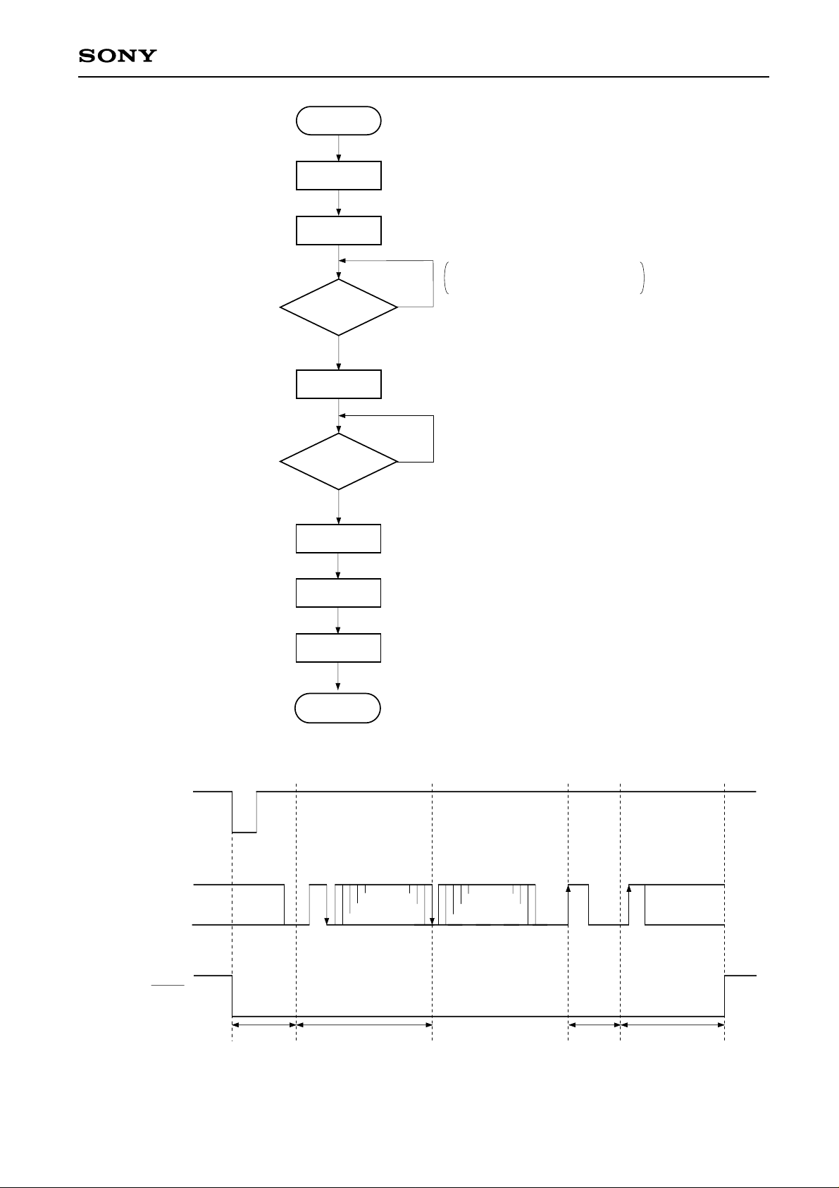
2N Track
Track, Sled
FWD Kick
WAIT
(Blind A)
CXD2500BQ
For the first 16 times CNIN is counted.
After that MIRR is counted.
CNIN (MIRR) =N
YES
Track, REV
Kick
C=Overflow
YES
Track Servo
ON
WAIT
(Klick D)
Sled Servo
ON
END
NO
NO
XLAT
CNIN
(MIRR)
BUSY
Figure 3-11 (a) Flow chart of 2N track jump
$4C (REV=$4D) latch
Blind A
$2A ($2F) $2E ($2B)
CNIN (MIRR)
N count
Figure 3-11 (b) Timing chart for 2N track jump
—42—
$26 ($27)Commands to SSP
Overflow
Kick D
$25
Page 43
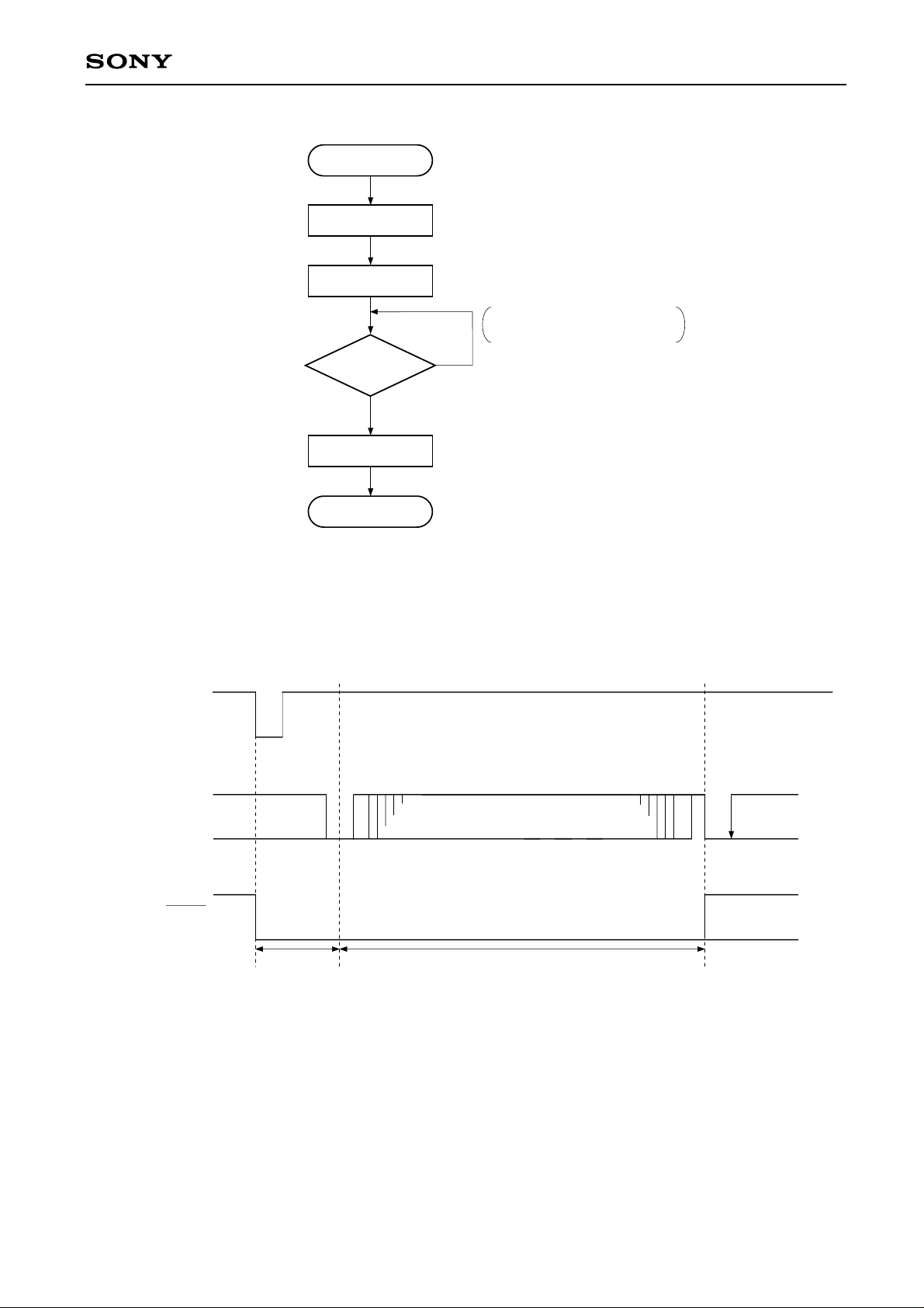
M Track move
Track Servo OFF
Sled FWD Kick
WAIT
(Blind A)
CNIN (MIRR) =M
YES
Track, Sled
Servo ON
END
NO
CNIN is counted for M<16, MIRR
is counted for M≥16.
CXD2500BQ
XLAT
CNIN
(MIRR)
BUSY
Figure 3-12 (a) Flow chart of M track move
$4E (REV=$4F) latch
Blind A
$22 ($23)Commands to SSP
CNIN (MIRR) M count
$25
Figure 3-12 (b) Timing chart for M track move
—43—
Page 44
CXD2500BQ
§3-7 Digital CLV
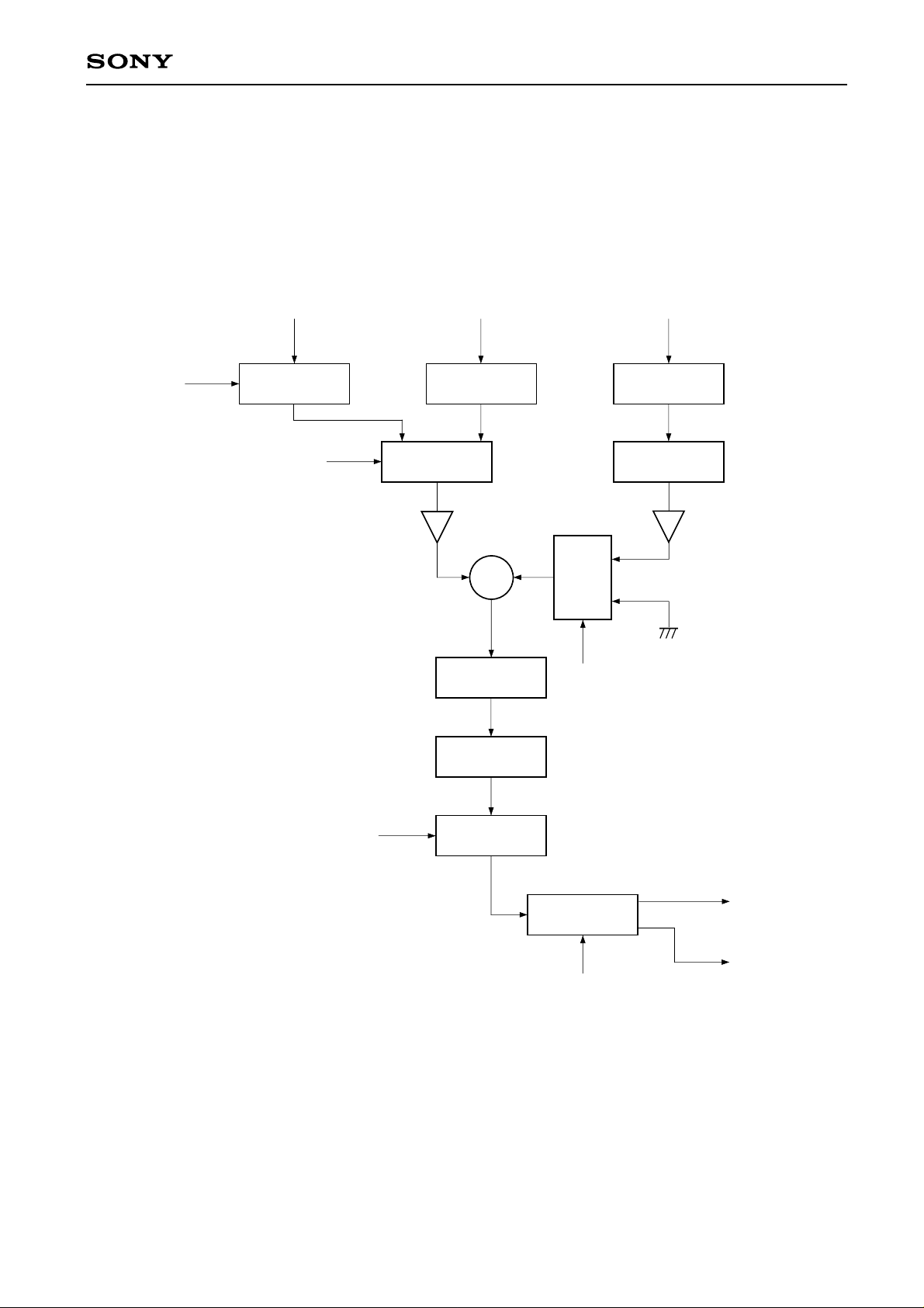
The digital CLV is a digital spindle servo, of which its block diagram is shown in Figure 3-14. It is capable of
outputting MDS or MDP error signals by the PWM method after raising the sampling frequency up to 130 kHz
based on the normal speed in the CLVS, CLVP and other modes. It also permits gain setting.
Digital CLV
CLVS U/D MDS Error MDP Error
Gain
CLV P/S
2/1 MUX
Measure
Gs(Gain)
+
Over Sampling
Filter-2
Noise Shape
Measure0, –6dB
Over Sampling
Filter-1
GP(Gain)
CLV P
1/2
Mux
CLV S
CLV – P/S
KICK, BRAKE STOP
Modulation
MDP
Mode Select
MDS
DCLVMD
Figure 3-14 Block diagram
—44—
Page 45
§3-8 Asymmetry correction
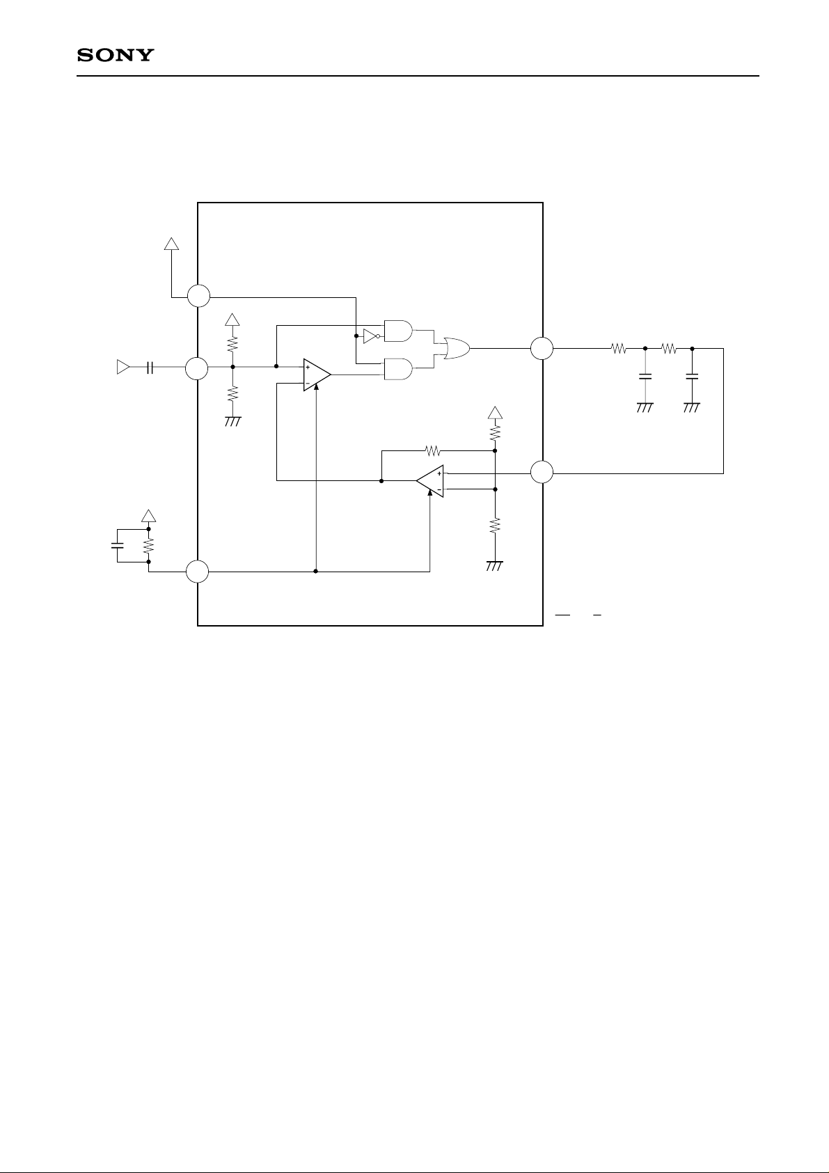
Block diagram and circuit example are shown on Fig. 3-15.
28
ASYE
RF
24
R1
R1
CXD2500BQ
D2500B
ASYO
27
BIAS
R2
25
R1
R1
Figure 3-15 Asymmetry correction application circuit example
26
ASYI
R1 2
=
R2 5
—45—
Page 46
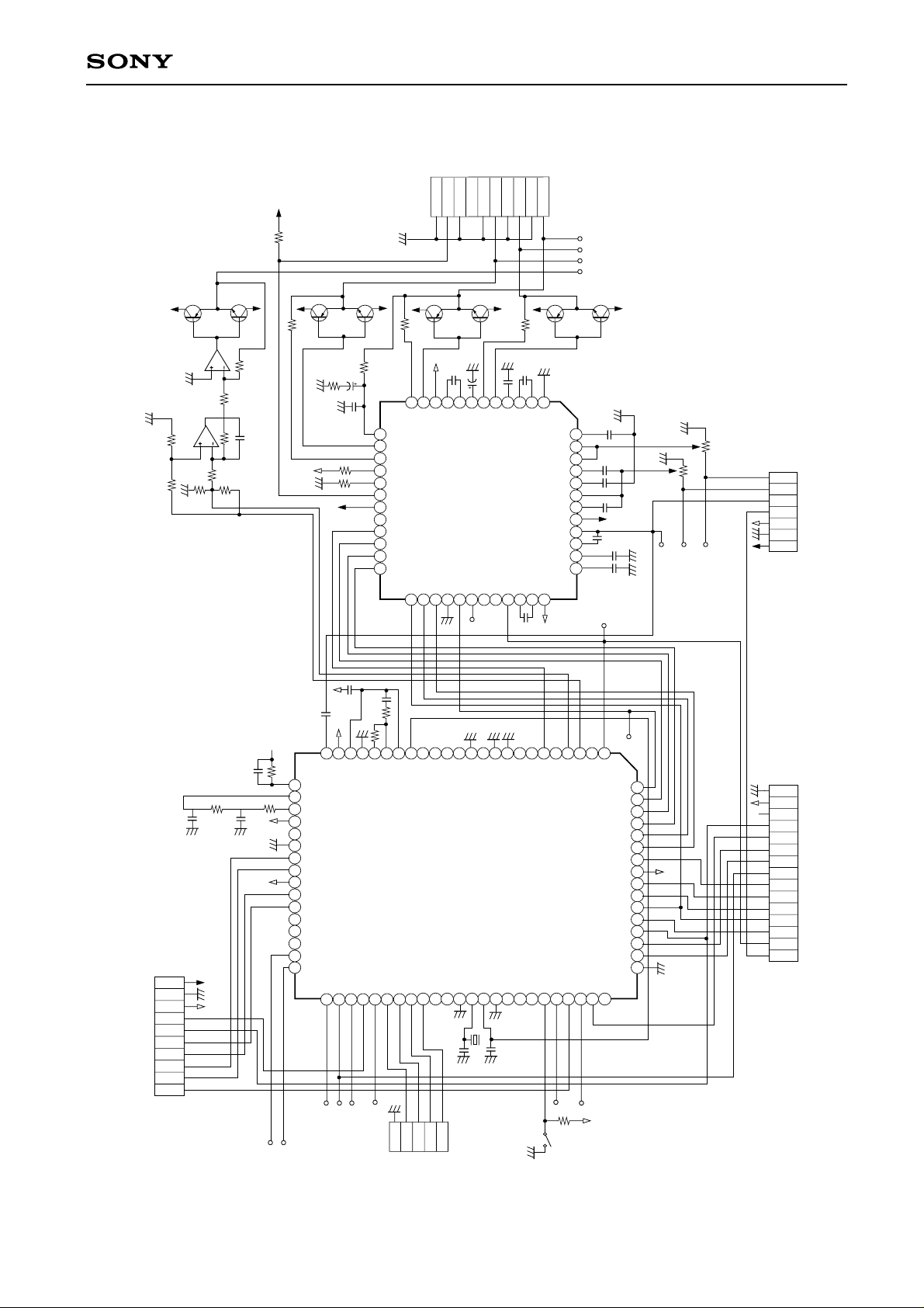
Application Circuit
GND
SSTOP
GND
SPIND-D
GND
SLED-D
GND
FOCUS-D
GND
TRACK-D
CXD2500BQ
GND
GND
R14
R13
GND
R5
R9
R10
C35
R11
R12
GND
GND
R6
GND
C28
C27
R4 R3
R2
GND
R7
SL+
14
SLO
SL-
FSET
ISET
SSTOP
191817161513
AVee
20
DIRC
21 2322
LOCK
CLK
XLT
DATA
12
TA-
XRST
25
11
TAO
COUT
26
C26
10
9
TG2
AV
CC
CXA1372Q
DGND
SENS
282427
C23
TGU
MIRR
29
SRCH
DFCT
30
DFCT
FE-
ASY
31
FEO
EFM
32
GND
45678
33
C10
FLB
FOK
GND
3
FS3
CC1
34
TD
FD
SLD
SPD
R1
GND
C9
2
FGD
CC2
35
1
VC
FDFCT
FZC
ATSC
TDFCT
TZC
DVee
RFO
DV
CC
36
RFI
FE
TE
CP
CB
GND
C12
48 47 46 45
C11
C13
44 40 39 38 37
43 42 41
C14
C15
C16
C17
FOK
GNDGND
GND
GND
RV1
RV2
FE
TE
RF
FE
TE
RF
LDON
V
CC
V
0
CC
V
Vee
GND
CC
V
C2PO
MUTE
BCLK
DATA
WDCK
LRCK
DEMP
GND
GND
GND
200p
AV
GND
GND
DD
1M
25 36
BIAS
26 33323130292827 3534 4039
ASTI
ASTO
ASYE
NC
PSSL
WDCK (48)
LRCK (48)
V
DD
DATA (64)
BCLK (64)
DATA (64)
BCLK (64)
3837
LRCK (64)
GTOP
XUGF
RF
PLCK
41
232224
GFS
42
AV
DD
CLTV
RFCK
43
21
AV
SS
C2PO
44
20
PCO
RADF
1918171615
FILO
VCKI
FILI
MNT1
MNT2
MNT3
48
47
464549
GND
VPCO
V
PDO
SS
11
12
13
14
NC
NC
NC
CXD2500BQ
MNT0
APTR
APTL
51
XTAO
XTAI
V
SS
54
53
52
GND
10
TEST1
XTSL
55
GND
9
VCOI
FSTT
56
VCOO
C4M
57
NC
C16M
58
LOCK
MO2
59
MOS
DOUT
60
45678
MOP
EMPH
61
3
MON
WFCK
625063
2
FSW
SCOR
1
FOK
MIRR
CLKO
XLTO
DATO
CNIN
CLOK
XLAT
DATA
XRST
SENS
MUTE
SQCK
SQSO
EXCK
SBSO
64
SEIN
V
MIRR
80 79 78 77 76 75 74
73
DD
72
71 70 69 68 67 66
GND
65
GND
CC
V
MUTE
SCOR
SQCK
SUBQ
GFS
CLK
XLT
DATA
XRST
SENS
FOK
LDON
GNDGND
GND
GND
DOUT
WFCK
STTP
UGFS
PLCK
GFS
RFCK
RAOV
GND
GND
MNT3
MNT2
MNT1
MNT0
GND
Application circuits shown are typical examples illustrating the operation of the devices. Sony cannot assume responsibility for
any problems arising out of the use of these circuits or for any infringement of third party and other right due to same.
—46—
Page 47
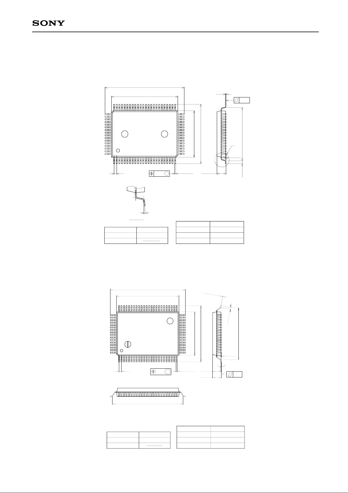
Package Outline Unit : mm
CXD2500BQ
CXD2500BQ
65
80
64
1
SONY CODE
EIAJ CODE
JEDEC CODE
0.8
23.9 ± 0.4
20.0 – 0.1
0° to 10°
DETAIL A
80PIN QFP (PLASTIC)
+ 0.4
0.12
M
QFP-80P-L01
∗QFP080-P-1420-A
41
40
+ 0.4
17.9 ± 0.4
14.0 – 0.1
25
24
+ 0.15
0.35 – 0.1
2.75 – 0.15
PACKAGE STRUCTURE
PACKAGE MATERIAL
LEAD TREATMENT
LEAD MATERIAL
PACKAGE WEIGHT
+ 0.1
0.15 – 0.05
+ 0.35
EPOXY RESIN
SOLDER PLATING
COPPER / 42 ALLOY
1.6g
A
+ 0.2
0.1 – 0.05
0.15
16.3
0.8 ± 0.2
CXD2500BQ
65
80
SONY CODE
EIAJ CODE
JEDEC CODE
80PIN QFP (PLASTIC)
24.0 ± 0.3
+ 0.4
20.0 – 0.1
4164
40
+ 0.4
14.0 – 0.1
25
1
0.8
± 0.12
22.6
24
+ 0.15
0.35 – 0.1
M
PACKAGE STRUCTURE
PACKAGE MATERIAL
QFP-80P-L121
∗QFP080-P-1420-AX
LEAD TREATMENT
LEAD MATERIAL
PACKAGE WEIGHT
0.15 – 0.05
18.0 ± 0.3
2.7 ± 0.1
3.1 MAX
+ 0.1
0.7 ± 0.1
+ 0.2
0.1 – 0.05
0° to 10°
EPOXY RESIN
SOLDER PLATING
42 ALLOY
1.6g
16.6
0.15
—47—
Page 48
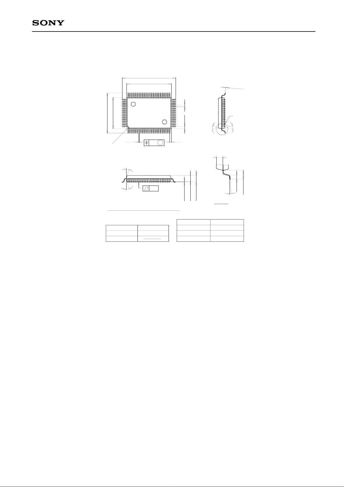
CXD2500BQ
CXD2500BQ
QFP 80PIN (PLASTIC)
23.9 ± 0.2
∗20.0 ± 0.2
64
65
41
40
0.8
0.15 ± 0.05
17.9 ± 0.2
∗14.0 ± 0.2
80
1
0.35 ± 0.1
C1.2
15°
15°
NOTE: Dimension “∗” does not include mold protrusion.
SONY CODE
EIAJ CODE
JEDEC CODE
0.15
M
0.15
QFP-80P-L051
∗QFP080-P-1420-AH
4 – 1.0
25
24
4 – 0.8
+ 0.20
2.7 – 0.16
2.94 ± 0.15
0.24 ± 0.15
PACKAGE STRUCTURE
PACKAGE MATERIAL
LEAD TREATMENT
LEAD MATERIAL
PACKAGE WEIGHT
15°
1.45
0° to 10°
DETAIL A
EPOXY RESIN
SOLDER PLATING
42 ALLOY
1.6g
A
15°
0.8 ± 0.15
1.95 ± 0.15
—48—
 Loading...