

Page 1
Timing Generator for LCD Panels
Description
The CXD2464R is a timing signal generator for
driving the LCX026, LCX016 and LCX012BL LCD
panels. This chip has a built-in serial interface circuit
which supports various XGA, SVGA and VGA signals,
and (double speed) NTSC and PAL signals through
external control from a microcomputer, etc.
Features
• Generates the LCX026/LCX016/LCX012BL drive
pulse.
• Supports various SVGA (horizontal scanning frequency:
35 to 54kHz, vertical scanning frequency: 56 to 86Hz)
and VGA (horizontal scanning frequency: 31 to 38kHz,
vertical scanning frequency: 59 to 75Hz) signals.
• Supports simple (skip scan) display of XGA signals
(1024 × 768 dots, horizontal scanning frequency:
57kHz, vertical scanning frequency: 71Hz or less,
clock frequency: 62.5MHz or less).
• Supports simple (skip scan) display of SVGA
signals (800 × 600 dots).
• Supports Macintosh16 signals (LCX016)
• Supports PC-98 signals (640 × 400 dots, horizontal
scanning frequency: 24 to 38kHz, vertical scanning
frequency: 56 to 86Hz).
• Supports NTSC and PAL signals
• Line double-speed display realized with a built-in
double-speed controller (clock frequency: 33.3MHz
or less)
(Line memory µPD485505: NEC)
• Allows control of sample-and-hold position of
CXA2112R sample-and-hold driver.
• Supports up/down inversion and/or right/left inversion.
• Supports line inversion and field inversion
• AC drive of LCD panels during no signal
Note) Supported signals vary according to LCD panel.
Applications
LCD projectors, etc.
Structure
Silicon gate CMOS IC
Absolute Maximum Ratings (Ta = 25°C, VSS = 0V)
• Supply voltage VDD VSS – 0.5 to +7.0 V
• Input voltage VI VSS – 0.5 to VDD + 0.5 V
• Output voltage VO VSS – 0.5 to VDD + 0.5 V
• Operating temperature
Topr –20 to +75 °C
• Storage temperature
Tstg –55 to +150 °C
Recommended Operating Conditions
• Supply voltage VDD 4.5 to 5.5 V
• Operating temperature
Topr –20 to +75 °C
– 1 –
E98327-PS
Sony reserves the right to change products and specifications without prior notice. This information does not convey any license by
any implication or otherwise under any patents or other right. Application circuits shown, if any, are typical examples illustrating the
operation of the devices. Sony cannot assume responsibility for any problems arising out of the use of these circuits.
CXD2464R
64 pin LQFP (Plastic)
Note) "Macintosh" is a registered trademark of Apple Computer Inc..
"PC-98" is a registered trademark of NEC.
"VGA" is a registered trademark of IBM Corp..
Other company names and product names, etc. contained in these materials are trademarks or registered trademarks
of the respective companies.
For the availability of this product, please contact the sales office.
Page 2
– 2 –
CXD2464R
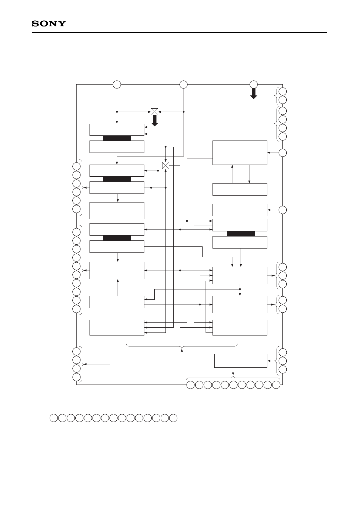
Block Diagram
1
4
5
6
7
8
9
10
11
12
13
14
15
16
18
23
24
35
40
55
56
SERIAL DATA I/F
50
51
52
53
38
54
57
58
59
63
20
21
22
25
26
37
45
46
47
48
49
60
61
62
33
34
41
43
44
27
28
29
30
31
32
36
39
42
41
19
17
64
VDD
VSS
VSYNC
HSYNC
VCK
VST
FLDO
FRP
XFRP
SCTR
SCLK
SDAT
XCLR
CKI1
CKI2
HD
RSTR
RCK
RSTW
WCK
HDN
HST
HCK1
HCK2
BLK
CLR
ENB
PCG
CLP1
CLP2
PRG
XVS
XHS
IRACT
ORACT
TEST
MODE3
MODE2
MODE1
RGT
XRGT
DWN
SHPA
SHPB
SHPC
SHPD
INV
SYSTEM CLEAR
V-SYNC SEPARATOR
V-RESET PULSE
GENERATOR
V-CONTROL COUNTER
H-SYNC DETECTOR
V-POSITION COUNTER
V POSITION DECODER
V-TIMING PULSE
GENERATOR
FIELD & LINE
CONTROLLER
AUX. V-COUNTER
DECODER
H-TIMING PULSE
GENERATOR
ADDITIONAL PULSE
GENERATOR
PULSE ELIMINATOR
H-POSITION DECODER
H-POSITION COUNTER
PLL PHASE
COMPARATOR
PLL COUNTER
PLL DECODER
AUX. PLL COUNTER
AUX. PLL DECODER
MASTER
CLOCK
2
3
Note) CLP2 and FLDO pulses share the same pins.
Page 3
– 3 –
CXD2464R
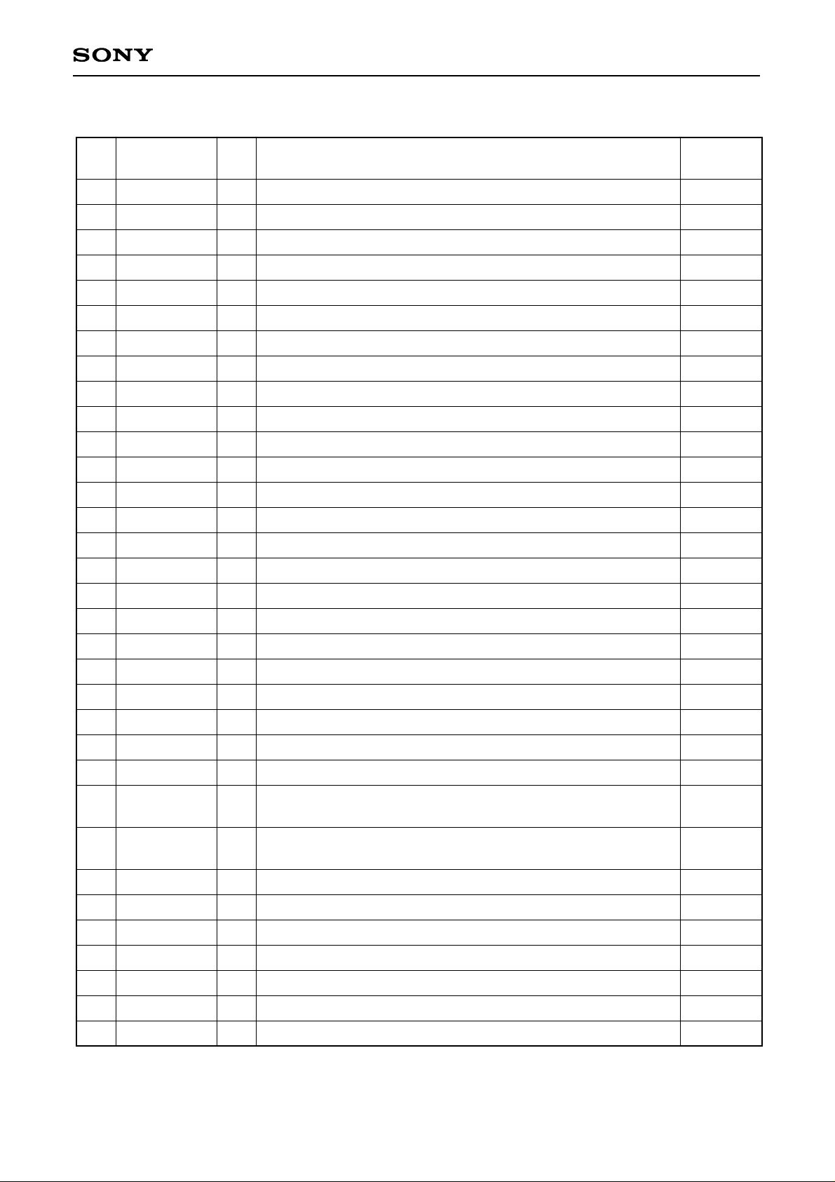
Pin Description
Pin
No.
Symbol
I/O Description
Input pin for
open status
1
2
3
4
5
6
7
8
9
10
11
12
13
14
15
16
17
18
19
20
21
22
23
24
25
26
27
28
29
30
31
32
33
HSYNC
VSYNC
TST0
TST1
TST2
TST3
TST4
VSS0
TST5
TST6
TST7
TST8
TST9
TST10
TST11
TST12
CKI2
TST13
XCLR
MODE3
MODE2
MODE1
VSS1
VDD0
RGT
XRGT
HST
HCK1
HCK2
BLK
CLR
ENB
VCK
I
I
—
—
—
—
—
—
—
—
—
—
—
—
—
—
I
I
I
O
O
O
—
—
O
O
O
O
O
O
O
O
O
Horizontal sync signal input pin
Vertical sync signal input pin
Test pin (Connect to GND.)
Test pin (Connect to VDD.)
Test pin (Not connected.)
Test pin (Connect to GND.)
Test pin (Not connected.)
GND
Test pin (Connect to GND.)
Test pin (Connect to VDD.)
Test pin (Not connected.)
Test pin (Not connected.)
Test pin (Not connected.)
Test pin (Not connected.)
Test pin (Not connected.)
Test pin (Connect to GND.)
Clock 2 input pin (for scan converter)
Test pin (Not connected.)
System clear pin (Set to L: SVGA (VESA 72Hz))
Mode switching pin 3 output
Mode switching pin 2 output
Mode switching pin 1 output
GND
VDD
Right/left inversion discrimination signal output
(H output: Normal, L output: Reverse)
Right/left inversion discrimination signal output
(H output: Reverse, L output: Normal)
HST pulse output
HCK 1 pulse output
HCK 2 pulse output
BLK pulse output
CLR pulse output
ENB pulse output
VCK pulse output
—
—
—
—
—
—
—
—
—
—
—
—
—
—
—
—
—
—
H
—
—
—
—
—
—
—
—
—
—
—
—
—
—
Page 4
– 4 –
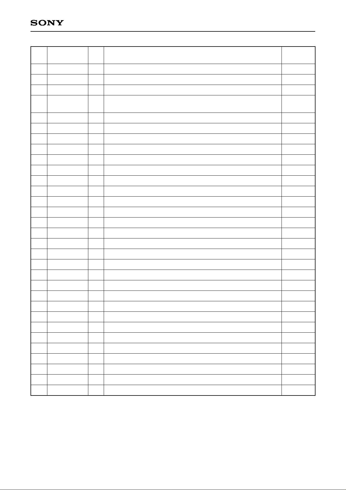
CXD2464R
Pin
No.
I/O
Description
Input pin for
open status
34
35
36
37
38
39
40
41
42
43
44
45
46
47
48
49
50
51
52
53
54
55
56
57
58
59
60
61
62
63
64
VST
TST14
PCG
DWN
HD
CLP1
VSS2
CLP2/FLDO
PRG
FRP
XFRP
SHPA
SHPB
SHPC
SHPD
INV
XVS
XHS
IRACT
ORACT
RSTR
VSS3
VDD1
RCK
RSTW
WCK
SCTR
SCLK
SDAT
HDN
CKI1
O
—
O
O
O
O
—
O
O
O
O
O
O
O
O
O
O
O
O
O
O
—
—
O
O
O
I
I
I
O
I
VST pulse output
Test pin (Not connected.)
PCG pulse output
Up/down inversion discrimination signal output
(H output: Down, L output: Up)
HD pulse output
Pedestal clamp pulse 1 output
GND
Pedestal clamp pulse 2 output/FLDO pulse output
Precharge signal pulse output
AC drive inversion timing output
AC drive inversion timing output (reverse polarity of FRP)
External sample-and-hold driver control signal (for CXA2112R)
External sample-and-hold driver control signal (for CXA2112R)
External sample-and-hold driver control signal (for CXA2112R)
External sample-and-hold driver control signal (for CXA2112R)
External sample-and-hold driver control signal (for CXA2112R)
Auxiliary pulse output for CXD2449Q
Auxiliary pulse output for CXD2449Q
Auxiliary pulse output for scan converter
Auxiliary pulse output for scan converter
Reset read output (for high-speed line buffer)
GND
VDD
Read clock output (for high-speed line buffer)
Reset write output (for high-speed line buffer)
Write clock output (for high-speed line buffer)
Chip select input pin (serial transfer block)
Serial clock input pin (serial transfer block)
Serial data input pin (serial transfer block)
Phase comparator pulse output
Clock 1 input pin
—
—
—
—
—
—
—
—
—
—
—
—
—
—
—
—
—
—
—
—
—
—
—
—
—
—
—
—
—
—
—
∗
H: Pull up, L: Pull down
Symbol
Page 5
– 5 –
CXD2464R
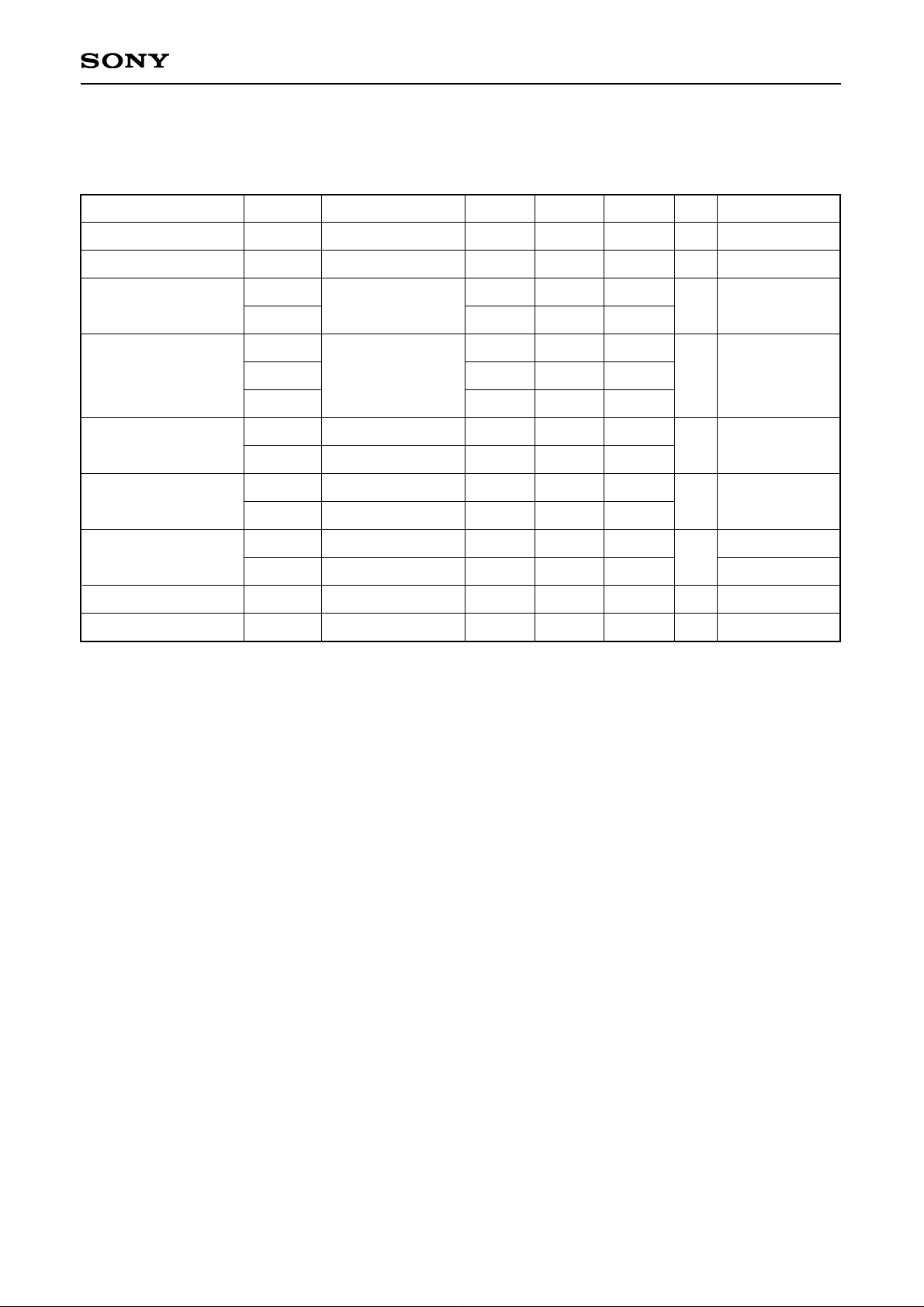
Electrical Characteristics
1. DC characteristics (VDD = 5.0 ± 0.5V, VSS = 0V, Topr = –20 to +75°C)
Item
Symbol
Min.
Typ. Max. UnitConditions
VDD
VI, Vo
VIH
VIL
Vt+
Vt–
Vt+ – Vt–
VOH
VOL
VOH
VOL
II
IIL
IOZ
IDD
CMOS input
IOH = –2mA
IOL = 4mA
IOH = –4mA
IOL = 8mA
∗3
∗5
∗6
∗8
4.5
VSS
0.7VDD
2.2
VDD – 0.8
VDD – 0.8
–10
–40
–40
5.0
0.4
–100
5.5
VDD
0.3VDD
0.8
0.4
0.4
10
–240
40
56
V
V
V
V
V
V
µA
µA
mA
Applicable pins
XCLR
CKI1, CKI2
HSYNC
VSYNC
SCTR, SCLK
SDAT
∗1
∗2
∗4
XCLR
∗7
At a 30pF load
∗1
INV, SHPA, SHPB, SHPC, SHPD, MODE1, MODE2, MODE3, HD, HDN, CLR, ENB, PRG, PCG, CLP1,
CLP2/FLDO, VST, BLK, FRP, XFRP, VCK, DWN, RGT, XRGT, IRACT, ORACT, XHS, XVS
∗2
RSTR, RSTW, RCK, WCK, HCK1, HCK2, HST
∗3
Normal input pins (VIN = VSS or VDD)
∗4
HSYNC, VSYNC, SCLK, SDAT, SCTR, CKI1, CKI2
∗5
Pins with pull-up resistors (VIN = VSS)
∗6
At high impedance (VIN = VSS or VDD)
∗7
SHPA, SHPC
∗8
fclk = 62.5MHz, VDD = 5.0V
Supply voltage
Input, output voltages
Input voltage 1
Input voltage 2
Output voltage 1
Output voltage 2
Input leak current
Output leak current
Current consumption
TTL Schmitt
trigger input
Page 6
– 6 –
CXD2464R
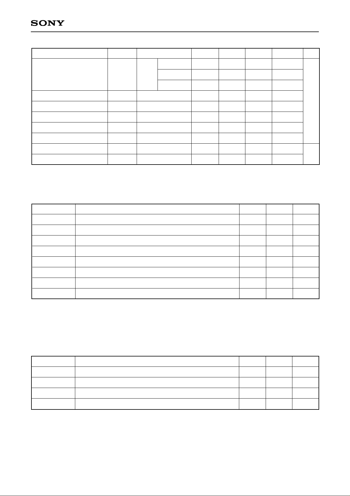
2. AC characteristics (VDD = 5.0 ± 0.5V, VSS = 0V, Topr = –20 to +75°C)
Item
Min. Typ.
Max. UnitConditions
Clock input cycle
Output rise time
Output fall time
Cross-point time difference
Output rise delay time
Output fall delay time
HCK1 Duty
HCK2 Duty
tr
tf
∆t
tpr
tpf
tH/(tH + tL)
tL/(tH + tL)
CL = 30pF
CL = 30pF
CL = 30pF
CL = 30pF
CL = 30pF
CL = 30pF
CL = 30pF
16.0
20.0
30.0
–10
48
48
20
20
10
15
15
52
52
ns
Symbol
CKI1, 2
All outputs
All outputs
HCK1, 2
All outputs
All outputs
HCK1
HCK2
Note) The minimum value for the clock input cycle (CKI1) when using the built-in double-speed controller is
30.0ns.
Note) During external clock input, set serial data HR to L. The pulse synchronized with the horizontal sync
signal is generated by detecting the front edge of horizontal sync signal and then resetting internal PLL
counter.
Note) Consider the frequency at free run (no signal). When the above characteristic specification is not
satisfied at free run, operating guarantee is not performed as serial transfer.
%
Applicable pins
3. Serial transfer AC characteristics (VDD = 5.0 ± 0.5V, Vss = 0V, Topr =–20 to +75°C)
Item Min. Typ. Max.
ts0
ts1
th0
th1
tw1L
tw1H
tw2
tw3
SCTR setup time with respect to rise of SCLK
SDAT setup time with respect to rise of SCLK
SCTR hold time with respect to rise of SCLK
SDAT hold time with respect to rise of SCLK
SCLK L level pulse width
SCLK H level pulse width
4Tns
2Tns
4Tns
2Tns
2Tns
2Tns
5Tns
5Tns
Symbol
T: Master clock cycle (ns)
4. External clock input AC characteristics (VDD = 5.0 ± 0.5V, Vss = 0V, Topr = –20 to +75°C)
Item Min. Typ. Max.
ts0
th0
twL
twH
HSYNC setup time with respect to rise of CKI1/2
HSYNC hold time with respect to rise of CKI1/2
CKI1/2 L level pulse width
CKI1/2 H level pulse width
2ns
6ns
6ns
6ns
T/2ns
T/2ns
Symbol
T: Master clock cycle (ns)
XGA, Mac16
SVGA
VGA
Page 7
– 7 –
CXD2464R
90%
10%
Note) HCK2 is the reverse phase of HCK1.
CKI1/2
Output
100%
tpr
10%
90%
tr
tf
tpf
V
DD
0V
V
DD
0V
V
DD
0V
Output
∆t
50%
HCK1
HCK2
50%
50% 50%
VDD
0V
V
DD
0V
50%50% 50%
HCK1
t
H tL
∆t
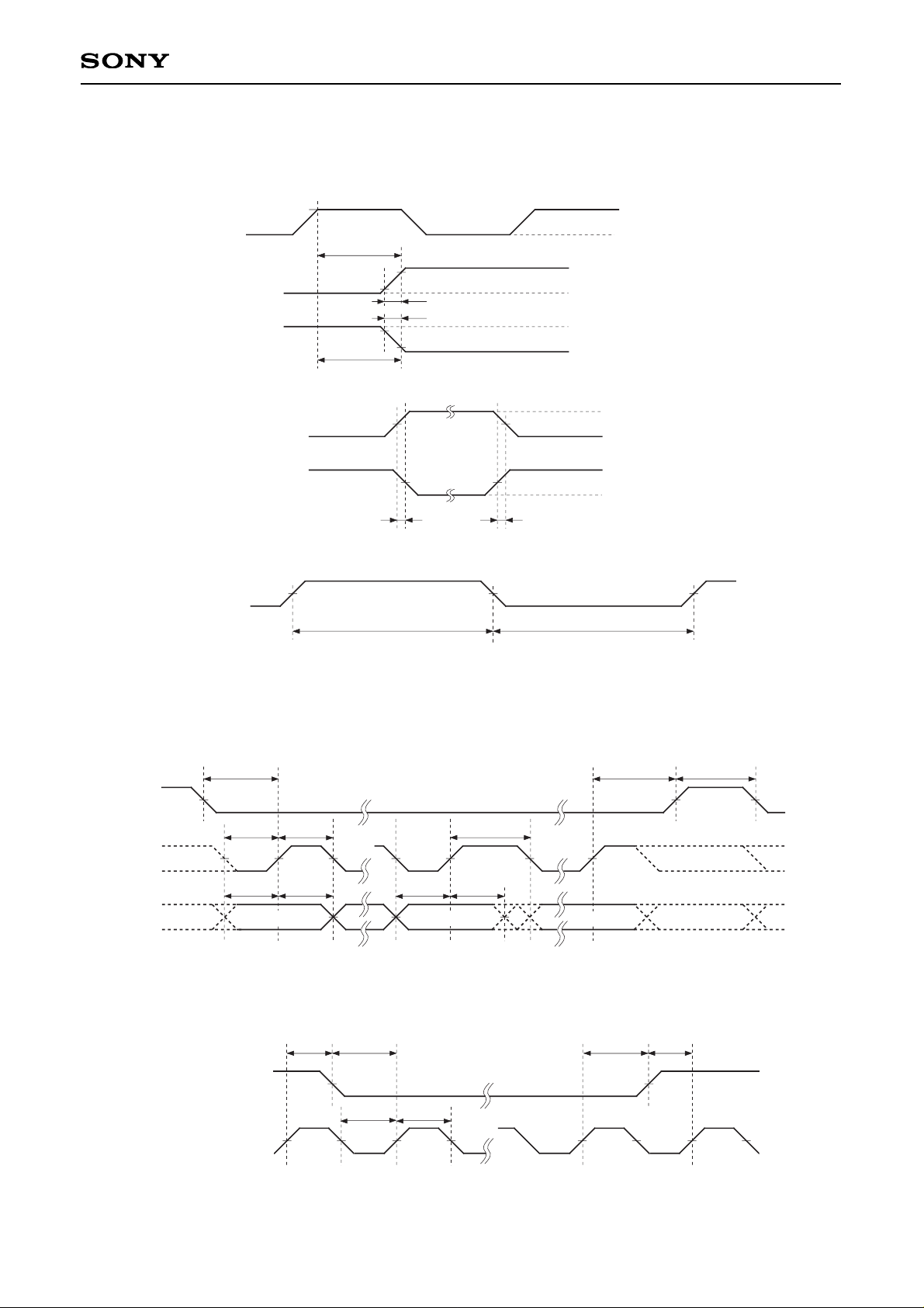
5. Timing definitions
AC characteristics
Serial transfer AC characteristics
External clock input AC characteristics
D7
D9
D14
SCLK
SDAT
50%
50%
50%
SCTR
ts0
th0
tw1L tw1H
ts1
th1
50%
50%
tw2
tw3
D15
Note) See "Serial transfer timing" for the timing relationship between D15 to D0 and each pulse.
ts1
th1
D0
D8
D15
CKI2
50%
HSYNC
(negative polarity)
th0
ts0 ts0th0
50% 50% 50%
twL twH
50%
50%
Page 8
– 8 –
CXD2464R
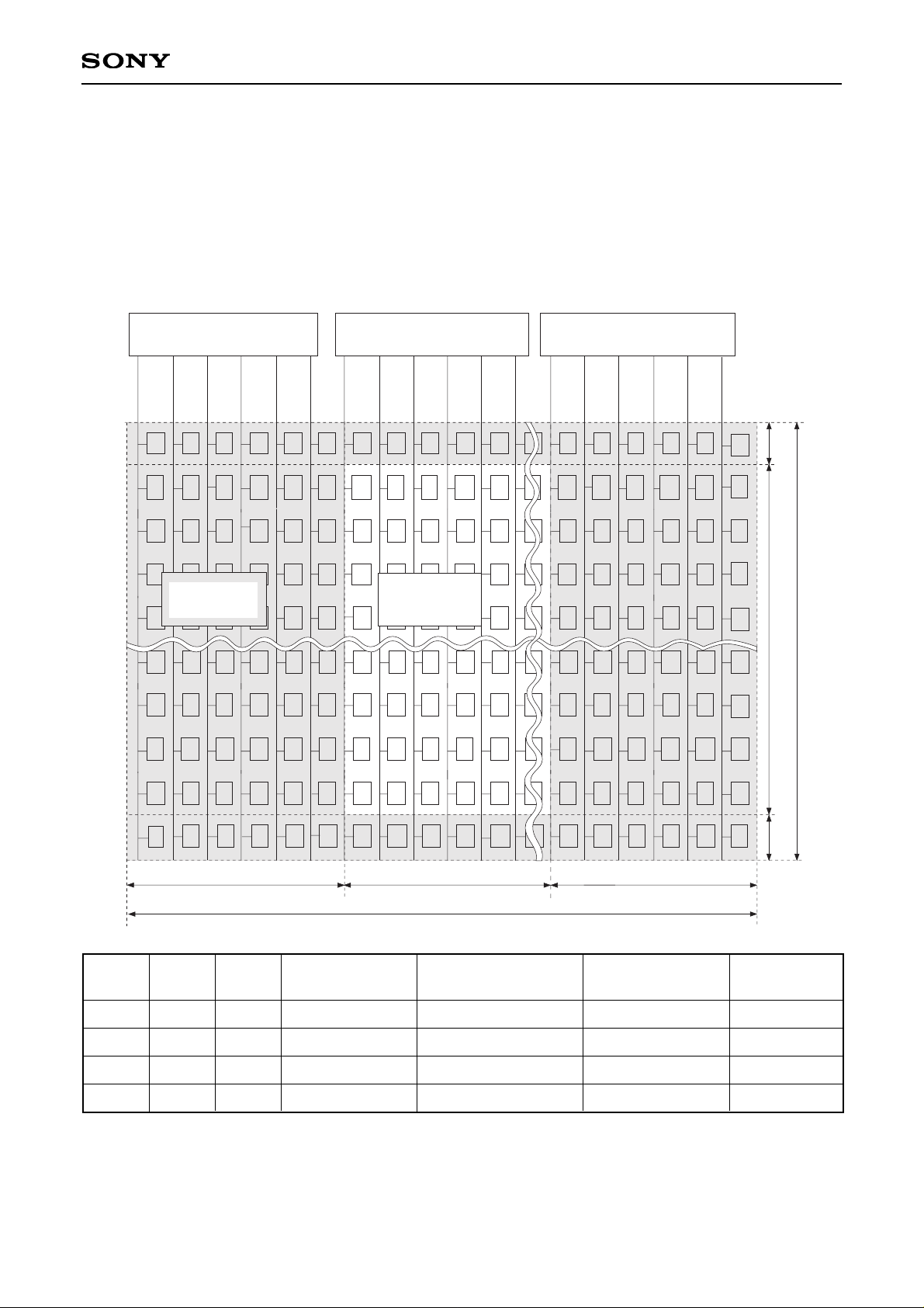
Pixel Arrangement
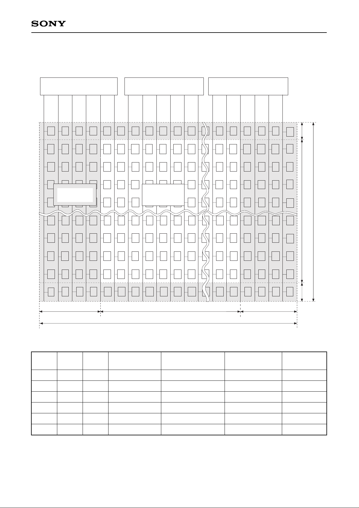
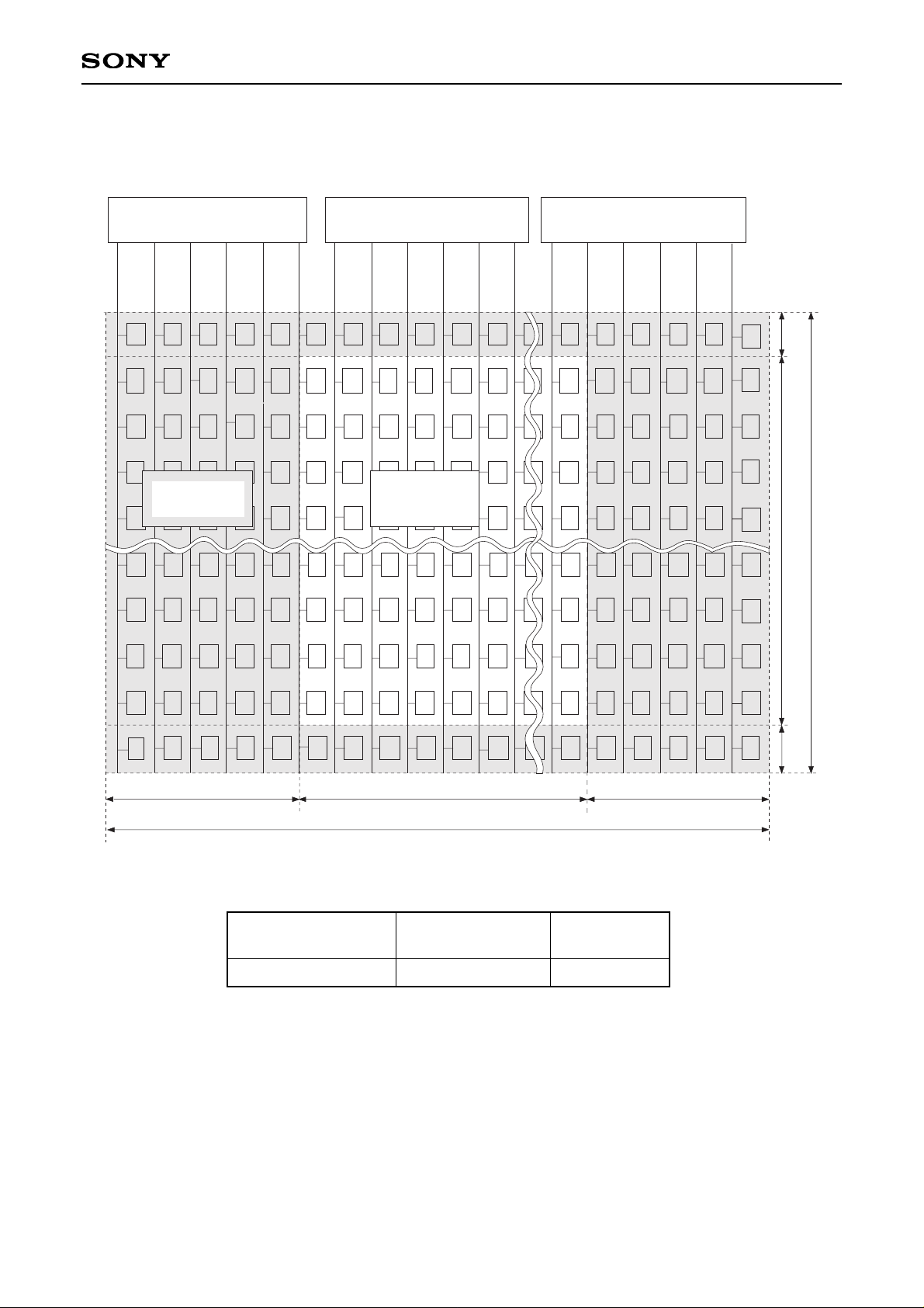
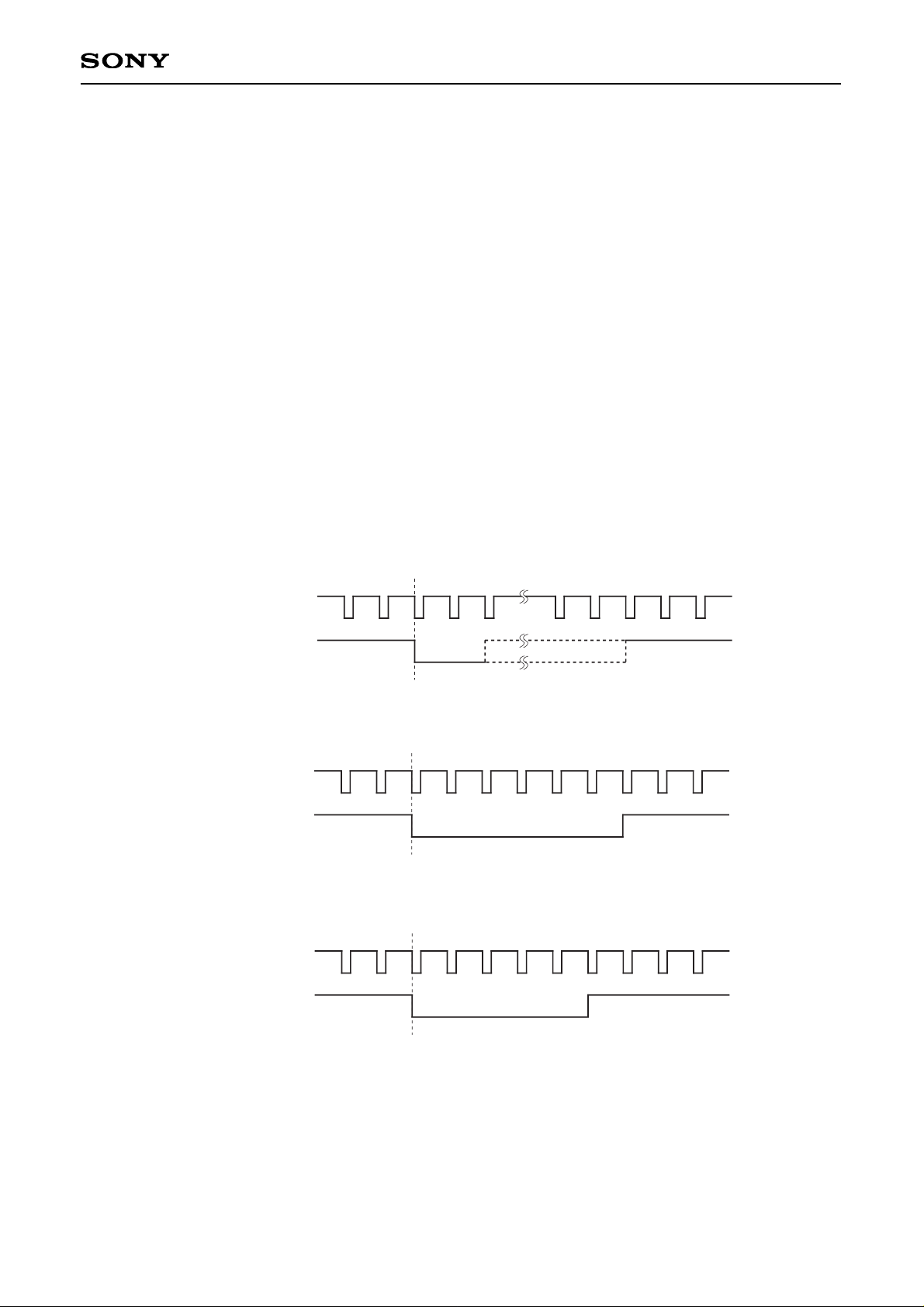
The LCD panels supported by the CXD2464R are the LCX026, the LCX016 and the LCX012BL. The pixel
arrangement is a square arrangement for both panels. The shaded region in the diagram is not displayed,
however, for the LCX026 and the LCX016, since the CXD2464R has a built-in display area variable circuit, the
display area dots varies according to the mode∗1to match the various signal protocols.
LCX026 pixel arrangement
MODE1 MODE2
MODE3
Display mode
Number of horizontal
display dots
Number of vertical
display dots
Number of
display dots
L
L
L
H
L
H
H
L
—
L
H
L
SVGA
PAL
VGA/NTSC
PC-98
804
762
644
644
604
572
484
404
485,616
435,864
311,696
260,176
∗1
See the description of serial data specifications for details.
Unit: dot—: don't care
Gate SW Gate SW Gate SW
1 dot
Photo-shielding
area
6 dots
Display area
804 dots
816 dots
6 dots
604 dots
1 dot
606 dots
Page 9
– 9 –
CXD2464R
LCX016 pixel arrangement
4 dots
840 dots
4 dots
626 dots
1 dot
1 dot
832 dots
624 dots
Gate SW Gate SW Gate SW
Display area
Photo-shielding
area
MODE1
MODE2 MODE3
L
L
L
L
H
H
L
L
H
H
L
L
L
H
L
H
L
H
Macintosh16
SVGA
PAL
VGA/NTSC
PC-98
WIDE
832
800
762
640
640
832
624
600
572
480
400
480
519,168
480,000
435,864
307,200
256,000
399,360
Unit: dot
Display mode
Number of horizontal
display dots
Number of vertical
display dots
Number of
display dots
Page 10
– 10 –
CXD2464R
LCX012BL pixel arrangement
5 dots
654 dots
5 dots
486 dots
1 dot
1 dot
644 dots
484 dots
Gate SW Gate SW Gate SW
Display area
Photo-shielding
area
Number of horizontal
display dots
644
Number of vertical
display dots
484
Number of
display dots
311,696
Unit: dot
Page 11
– 11 –
CXD2464R
Input Signal Protocol
1. Horizontal sync signal
a) A standard signal (HSYNC) should be input for the following display modes.
LCX026 : SVGA (800 × 600), VGA/NTSC (640 × 480), PC-98 (640 × 400), PAL (762 × 572)
LCX016 : Macintosh16 (832 × 624), SVGA (800 × 600), VGA/NTSC (640 × 480), PC-98 (640 × 400),
PAL (762 × 572), WIDE (832 × 480)
LCX012BL: VGA/NTSC/PAL (640 × 480), PC-98 (640 × 400)
However, since the CXD2464R requires a double speed signal as input during NTSC/PAL doublespeed display when not using the built-in double-speed controller, a simply double-speeded, 1/2 cycle,
1/2 width horizontal sync signal (HSYNC) should be input at that time.
b) The input sync signal polarity is not fixed, and is set by the serial data (HPOL).
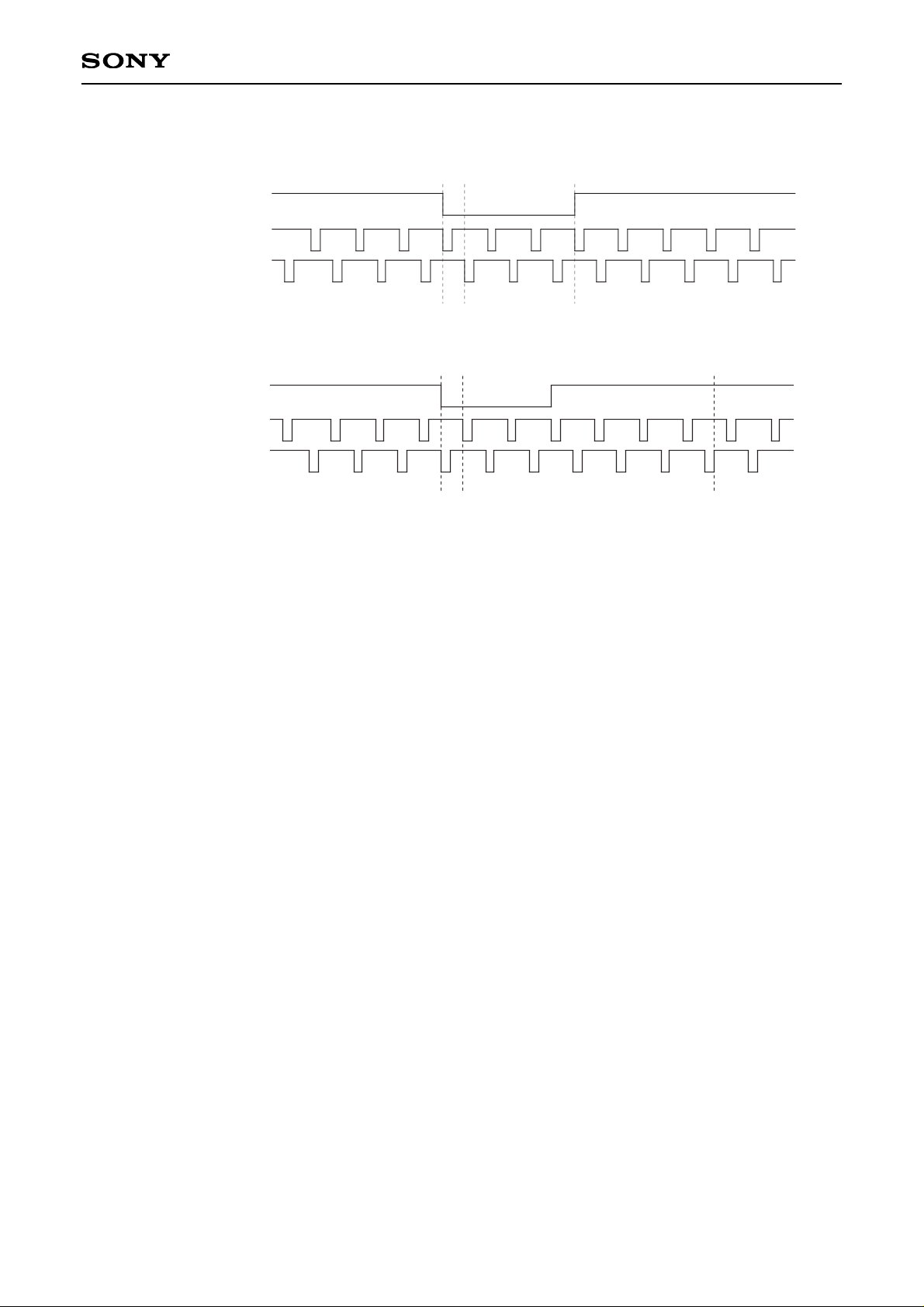
2. Vertical sync signal
a) A sync-separated, normal-speed VSYNC should be input as the vertical sync signal.
b) The input sync signal polarity is not fixed, and is set by the serial data (VPOL).
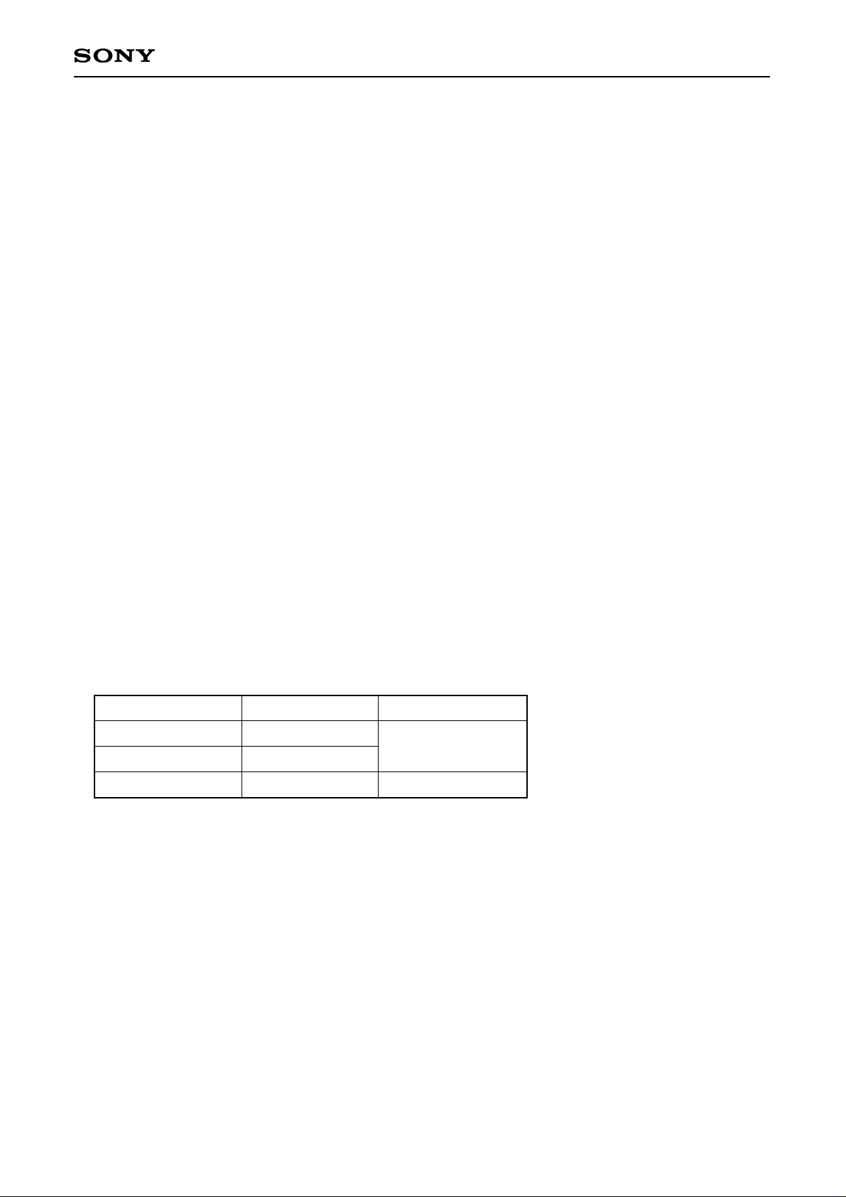
c) The phase relationship between HSYNC and VSYNC is specified as follows for the CXD2464R.
(1) SVGA, VGA, PC-98 (LCX026)/Macintosh16, SVGA, VGA, PC-98 (LCX016)/VGA, PC-98 (LCX012BL)
(2) Double-speed NTSC (LCX026/LCX016/LCX012BL)
(3) Double-speed PAL (LCX026/LCX016/LCX012BL)
HSYNC
VSYNC
Sync signal phase reference
Double-speed HSYNC
VSYNC
Sync signal phase reference
VSYNC
Double-speed HSYNC
Sync signal phase reference
Page 12
– 12 –
CXD2464R
(4) NTSC (LCX026/LCX016/LCX012BL)
ODD FIELD
EVEN FIELD
VSYNC
HSYNC
Sync signal phase reference
(5) PAL (LCX026/LCX016/LCX012BL)
ODD FIELD
EVEN FIELD
VSYNC
HSYNC
Sync signal phase reference
Note) (2) and (3) show the timing when supporting input of double-speed signals
(4) and (5) show the timing when using the built-in double-speed controller (CXD2464R) and a line
memory (µPD485505: NEC)
Page 13
– 13 –
CXD2464R
Description of Operation
Sync signal input
The HSYNC and VSYNC input pins support separate SYNC only. When using a composite SYNC input, use a
separate IC for sync separation, etc.
Clock input
(1) CKI1 pin
CKI1 is the clock input pin from an external PLL IC. A 1/N frequency divider output for PLL IC is output
from the HDN pin. HDN polarity at this time is set by serial data HDNPOL.
(2) CKI2 pin
CKI2 is a clock input pin when using a scan converter that operates with synchronous input signals and
asynchronous clock in the system. Since two types of clocks are input in this case, the circuit that basically
operates with the respective clocks of CKI1 and CKI2 is asynchronous. For details, refer to the explanation
of pulse setting for the scan converter in this specification (starting on page 37).
AC driving of LCD panels for no signal
The following measures have been adopted to allow AC driving of LCD panels even when there is no signal.
Horizontal direction pulse
The PLL is set to free running status. Therefore, the frequency of the horizontal direction pulse is
dependent on the PLL free running frequency.
Vertical direction pulse
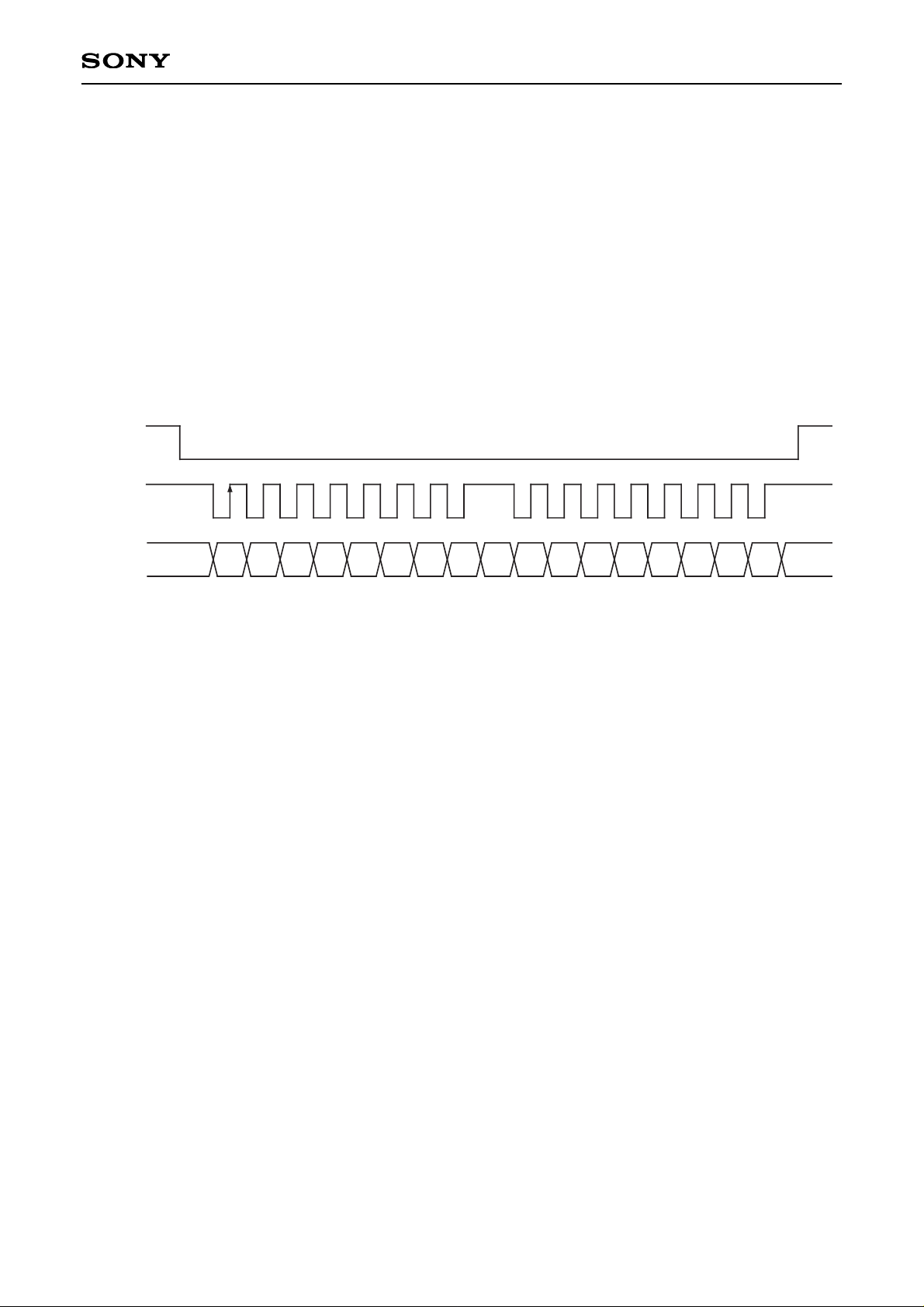
The number of lines is counted by an internal counter (AUX-VD COUNTER) and the vertical direction
pulses (VST, FRP) are output at a specified cycle. For the CXD2464R, no signal (free running) status is
judged if there is no VSYNC input for longer than the following periods (free running detection timing).
Mode
Double-speed NTSC
Double-speed PAL
Other
V cycle for no signal
263H
313H
650H
Free running detection
468H
900H
Note) The double-speed NTSC and PAL modes are the modes when using the built-in double-speed
controller.
Page 14
– 14 –
CXD2464R
XCLR pin
The CXD2464R should be forcibly reset during power on in order to initialize the serial transfer block and other
internal circuits.
Serial transfer operation
1. Control method
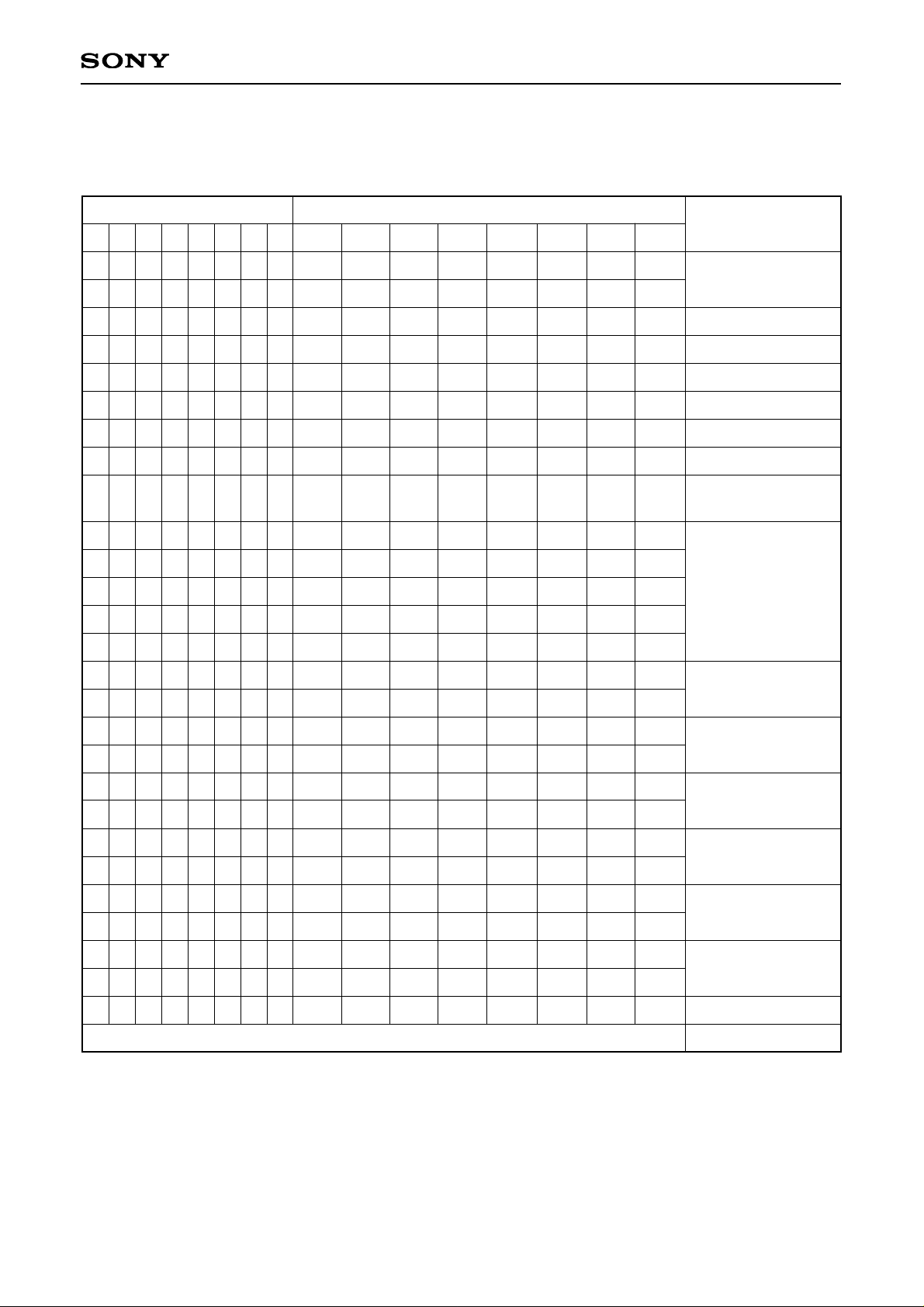
The CXD2464R operation timing is controlled by serial data.
The control data is comprised of an 8-bit address and 8-bit data, and the individual data is loaded at the rise of
SCLK. This load operation starts from the fall of SCTR and is completed at the next rise of SCTR.
Serial transfer timing
SCTR
SCLK
SDAT
Address
Data
D0D1D2D3D4D5D6D7D8D9D10D11D12D13D14D15
Page 15
– 15 –
CXD2464R
2. Control data
When using the CXD2464R, set the control data corresponding to each signal source according to the formats
in the table below.
D15
0
0
0
0
0
0
0
0
0
0
0
0
0
0
0
0
0
0
0
0
0
0
0
0
0
0
0
0
0
0
0
0
0
0
0
0
0
0
0
0
0
0
0
0
0
0
0
0
0
0
0
0
0
0
0
0
0
0
0
0
0
0
0
0
0
0
0
0
0
0
0
0
0
0
0
0
0
0
0
0
0
0
0
0
0
0
0
0
0
0
0
0
0
0
0
1
1
1
1
1
1
1
1
1
1
1
1
1
0
0
0
0
0
0
0
0
1
1
1
1
1
1
0
0
0
0
0
0
0
0
1
1
1
1
1
0
0
0
0
1
1
1
1
0
0
0
0
1
1
0
0
0
0
1
1
1
1
0
0
0
0
1
0
0
1
1
0
0
1
1
0
0
1
1
0
0
0
0
1
1
0
0
1
1
0
0
1
1
0
0
1
0
1
0
1
0
1
0
1
0
1
0
1
0
1
0
1
0
1
0
1
0
1
0
1
0
—
PLLP7
HP7
VP7
—
—
—
—
—
—
—
—
—
VGAV
—
IRD7
—
IRU7
ORRS3
ORP7
—
ORD7
—
ORU7
—
HPRS7
—
—
PLLP6
HP6
VP6
—
—
—
—
—
—
—
—
—
HR
—
IRD6
—
IRU6
ORRS2
ORP6
—
ORD6
—
ORU6
—
HPRS6
—
—
PLLP5
HP5
VP5
—
—
—
—
—
CKTST0
VPOL
—
MODE021
DWN
—
IRD5
—
IRU5
ORRS1
ORP5
—
ORD5
—
ORU5
—
HPRS5
—
—
PLLP4
HP4
VP4
—
PCGP4
PRGP4
—
INV
FLD
HPOL
MBKB
MODEB
RGT
SLLAP
IRD4
—
IRU4
ORRS0
ORP4
—
ORD4
—
ORU4
—
HPRS4
—
—
PLLP3
HP3
VP3
HSTP3
PCGP3
PRGP3
—
SHP3
FRP1
HDNPOL
MBKA
MODEA
HST
—
IRD3
—
IRU3
—
ORP3
—
ORD3
—
ORU3
—
HPRS3
—
PLLP10
PLLP2
HP2
VP2
HSTP2
PCGP2
PRGP2
—
SHP2
FRP0
CLPPOL
MBK2
MODE3
PCG
IRD10
IRD2
IRU10
IRU2
ORP10
ORP2
ORD10
ORD2
ORU10
ORU2
HPRS10
HPRS2
—
PLLP9
PLLP1
HP1
VP1
HSTP1
PCGP1
PRGP1
CLPP1
SHP1
CKTST1
PCGPOL
MBK1
MODE2
DSP
IRD9
IRD1
IRU9
IRU1
ORP9
ORP1
ORD9
ORD1
ORU9
ORU1
HPRS9
HPRS1
—
PLLP8
PLLP0
HP0
VP0
HSTP0
PCGP0
PRGP0
CLPP0
SHP0
RCK
PRGPOL
MBK0
MODE1
PC98
IRD8
IRD0
IRU8
IRU0
ORP8
ORP0
ORD8
ORD0
ORU8
ORU0
HPRS8
HPRS0
PRE
D14 D13 D12 D11 D10
D9 D8 D7 D6 D5 D4 D3 D2 D1 D0
Note) PLLP0, HP0, VP0, HSTP0, PCGP0, PRGP0, CLPP0, SHP0, IRD0, IRU0, ORRS0, ORP0, ORD0,
ORU0, HPRS0: LSB
Address
Data
Function
Settings other than those above are invalid
(A) PLL frequency
division ratio (1/N)
(B) H-POSITION
(C) V-POSITION
(D) HST-POSITION
(E) PCG-POSITION
(E) PRG-POSITION
(F) CLP-POSITION
(G) S/H control for
CXD2112R
(H) Mode settings
(I) IRACT fall position
(I) IRACT rise position
(J) ORACT reset cycle
ORACT frequency
(K) ORACT fall
position
(K) ORACT rise
position
(L) H position counter
reset position
(M) Preset
—
Page 16

– 16 –
CXD2464R
Each control data is described in detail below. (A) to (M)
(A) PLLP10, 9, 8, 7, 6, 5, 4, 3, 2, 1, 0
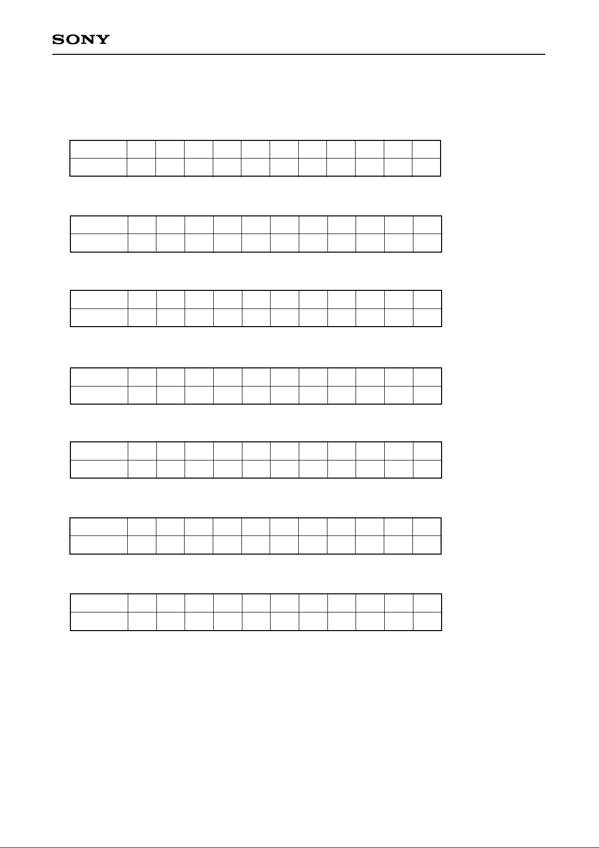
These bits set the frequency division ratio (master clock) of the internal 1/N frequency divider for the PLL. The
data is 11 bits and the frequency division ratio can be set up to 2048. The actual frequency division ratio
should be set as follows.
Number of clk for the horizontal period – 2 = Actual number of dots set
Examples of settings for major modes are shown below.
Examples using the LCX026
1) SVGA (800 × 600)
PLLP setting value = 1040 (horizontal period) – 2 → 1038 (HLLLLLLHHHL: LSB)
2) VGA (640 × 480)
PLLP setting value = 832 (horizontal period) – 2 → 830 (LHHLLHHHHHL: LSB)
3) PC-98 (640 × 400)
PLLP setting value = 848 (horizontal period) – 2 → 846 (LHHLHLLHHHL: LSB)
4) NTSC (640 × 480)
PLLP setting value = 1560 (horizontal period) – 2 → 1558 (HHLLLLHLHHL: LSB)
5) PAL (762 × 572)
PLLP setting value = 1880 (horizontal period) – 2 → 1878 (HHHLHLHLHHL: LSB)
PLLP 10 9 8 7 6 5 4 3 2 1 0
Setting data H L L L L L L H H H L
PLLP 10 9 8 7 6 5 4 3 2 1 0
Setting data L H H L L H H H H H L
PLLP 10 9 8 7 6 5 4 3 2 1 0
Setting data L H H L H L L H H H L
PLLP 10 9 8 7 6 5 4 3 2 1 0
Setting data H H L L L L H L H H L
PLLP 10 9 8 7 6 5 4 3 2 1 0
Setting data H H H L H L H L H H L
∗
VESA VGA72
∗
VESA SVGA72
Page 17
– 17 –
CXD2464R
Examples using the LCX016
1) Macintosh16 (832 × 624)
PLLP setting value = 1152 (horizontal period) – 2 → 1150 (HLLLHHHHHHL: LSB)
2) SVGA (800 × 600)
PLLP setting value = 1040 (horizontal period) – 2 → 1038 (HLLLLLLHHHL: LSB)
3) VGA (640 × 480)
PLLP setting value = 832 (horizontal period) – 2 → 830 (LHHLLHHHHHL: LSB)
4) PC-98 (640 × 400)
PLLP setting value = 848 (horizontal period) – 2 → 846 (LHHLHLLHHHL: LSB)
5) NTSC WIDE (832 × 480)
PLLP setting value = 1014 (horizontal period) – 2 → 1012 (LHHHHHHLHLL: LSB)
6) NTSC (640 × 480)
PLLP setting value = 1560 (horizontal period) – 2 → 1558 (HHLLLLHLHHL: LSB)
7) PAL (762 × 572)
PLLP setting value = 1880 (horizontal period) – 2 → 1878 (HHHLHLHLHHL: LSB)
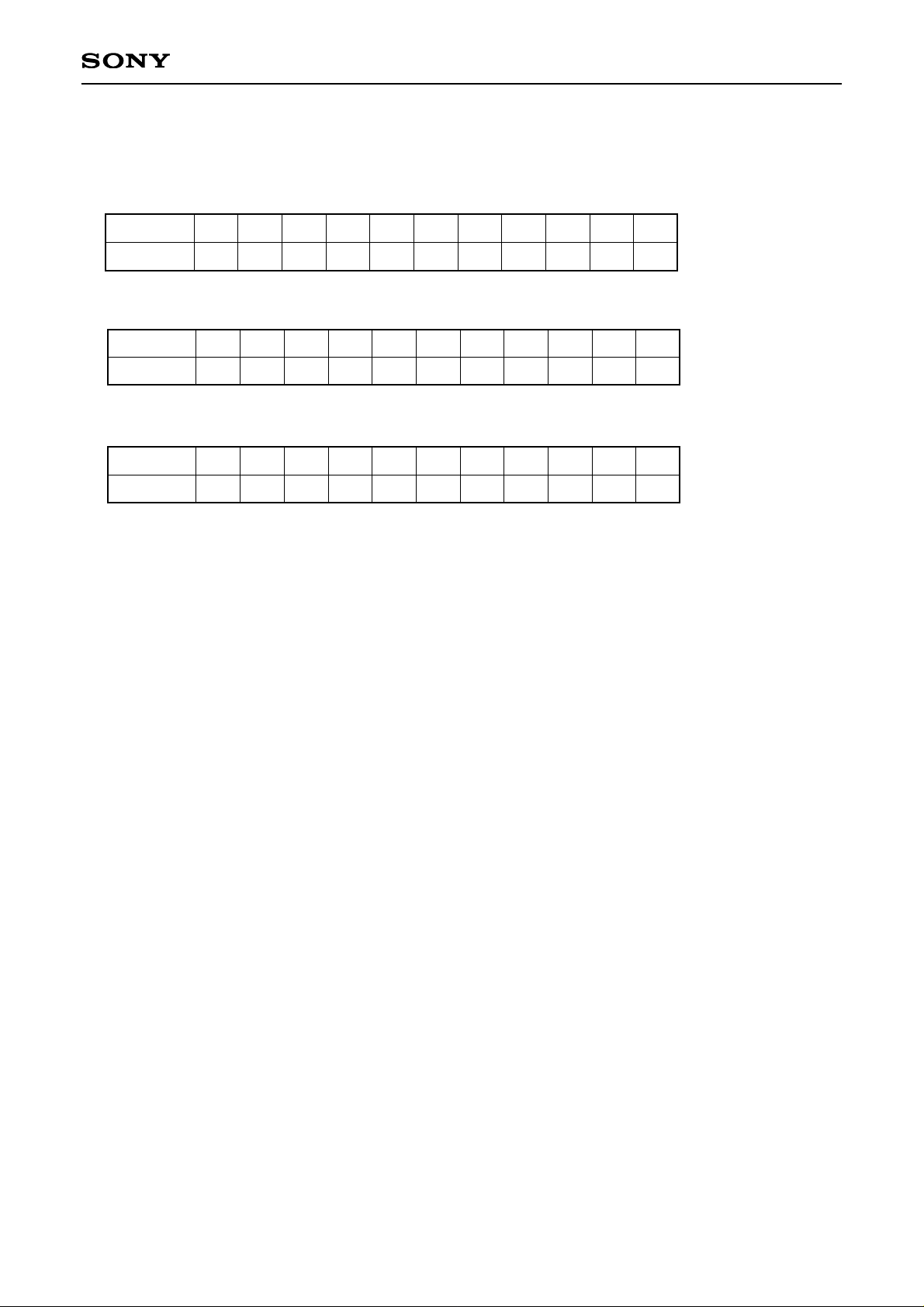
PLLP 10 9 8 7 6 5 4 3 2 1 0
Setting data H L L L H H H H H H L
PLLP 10 9 8 7 6 5 4 3 2 1 0
Setting data H L L L L L L H H H L
PLLP 10 9 8 7 6 5 4 3 2 1 0
Setting data L H H L L H H H H H L
PLLP 10 9 8 7 6 5 4 3 2 1 0
Setting data L H H L H L L H H H L
PLLP 10 9 8 7 6 5 4 3 2 1 0
Setting data L H H H H H H L H L L
PLLP 10 9 8 7 6 5 4 3 2 1 0
Setting data H H L L L L H L H H L
PLLP 10 9 8 7 6 5 4 3 2 1 0
Setting data H H H L H L H L H H L
∗
VESA SVGA72
∗
VESA VGA72
Page 18
– 18 –
CXD2464R
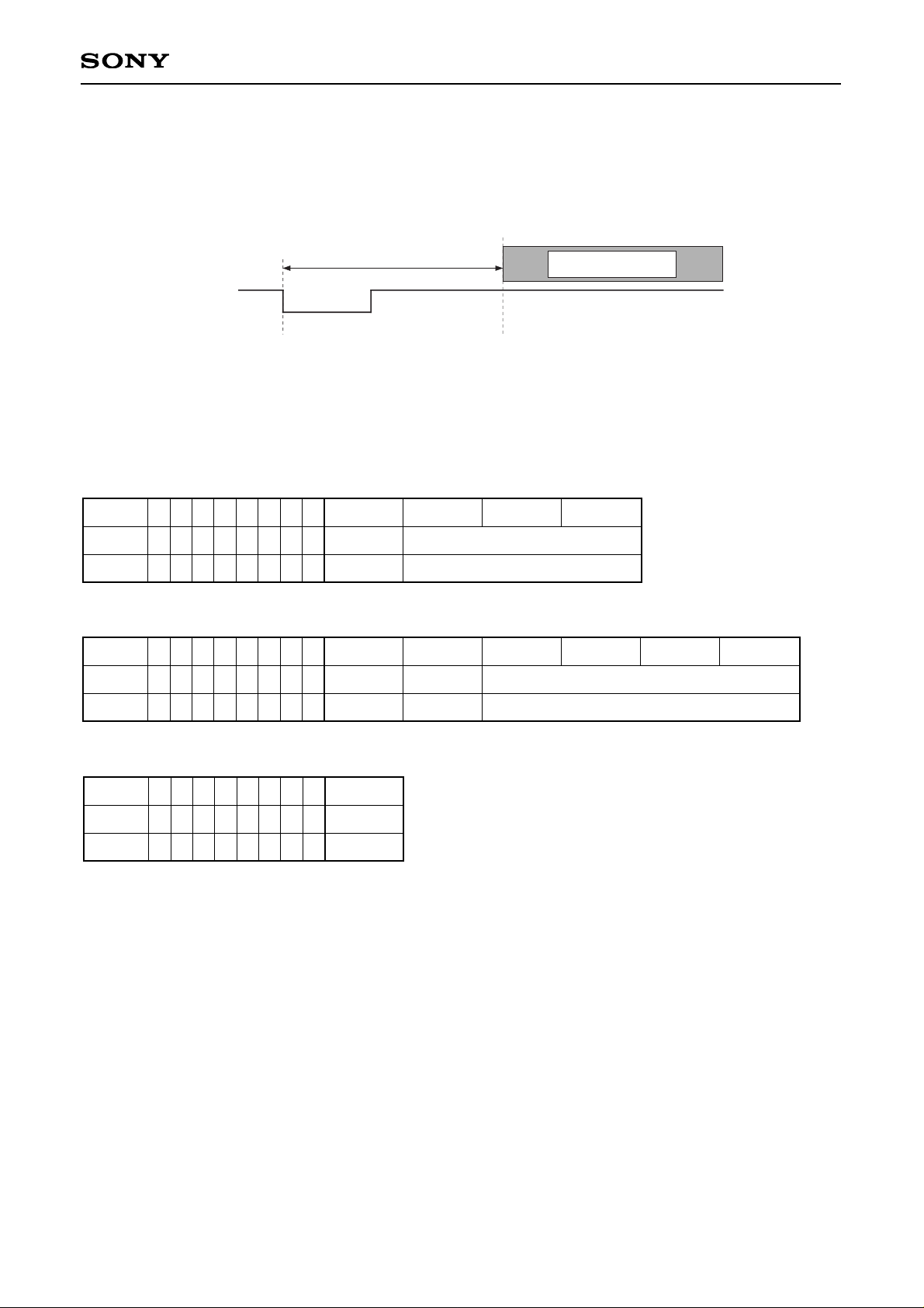
Examples using the LCX012BL
1) VGA (640 × 480)
PLLP setting value = 896 (horizontal period) – 2 → 894 (LHHLHHHHHHL: LSB)
2) PC-98 (640 × 400)
PLLP setting value = 848 (horizontal period) – 2 → 846 (LHHLHLLHHHL: LSB)
3) NTSC, PAL (640 × 480)
PLLP setting value = 1560 (horizontal period) – 2 → 1558 (HHLLLLHLHHL: LSB)
PLLP 10 9 8 7 6 5 4 3 2 1 0
Setting data L H H L H H H H H H L
PLLP 10 9 8 7 6 5 4 3 2 1 0
Setting data L H H L H L L H H H L
PLLP 10 9 8 7 6 5 4 3 2 1 0
Setting data H H L L L L H L H H L
∗
VESA VGA72
Page 19
– 19 –
CXD2464R
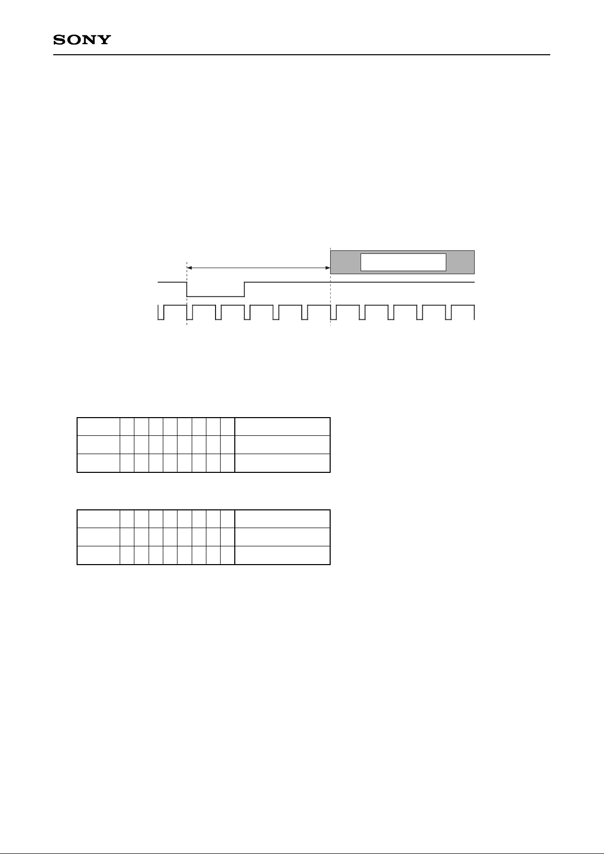
(B) HP7, 6, 5, 4, 3, 2, 1, 0
These bits set the horizontal display start position. The minimum adjustment width is 1 dot, and adjustment
of up to 256 clk with 8 bits is possible using the front edge of HSYNC as the reference.
Thp
HSYNC
Image display period
Thp: Timing from the edge of HSYNC to the start of image display
Minimum and maximum Thp setting values for each mode
LCX026
LCX016
LCX012BL
HP 7 6 5 4 3 2 1 0
800 × 600 762 × 572 640 × 480 640 × 400
Min.
Max.HL L L L L L L L 416 clk 370 clk
H H H H H H H 161 clk 115 clk
HP 7 6 5 4 3 2 1 0
832 × 624 800 × 600 762 × 572 640 × 480 640 × 400 832 × 480
Min.
Max.HL L L L L L L L 440 clk 410 clk 364 clk
H H H H H H H 185 clk 155 clk 109 clk
HP 7 6 5 4 3 2 1 0
644 × 484
Min.
Max.HL L L L L L L L 367 clk
H H H H H H H 112 clk
Page 20
– 20 –
CXD2464R
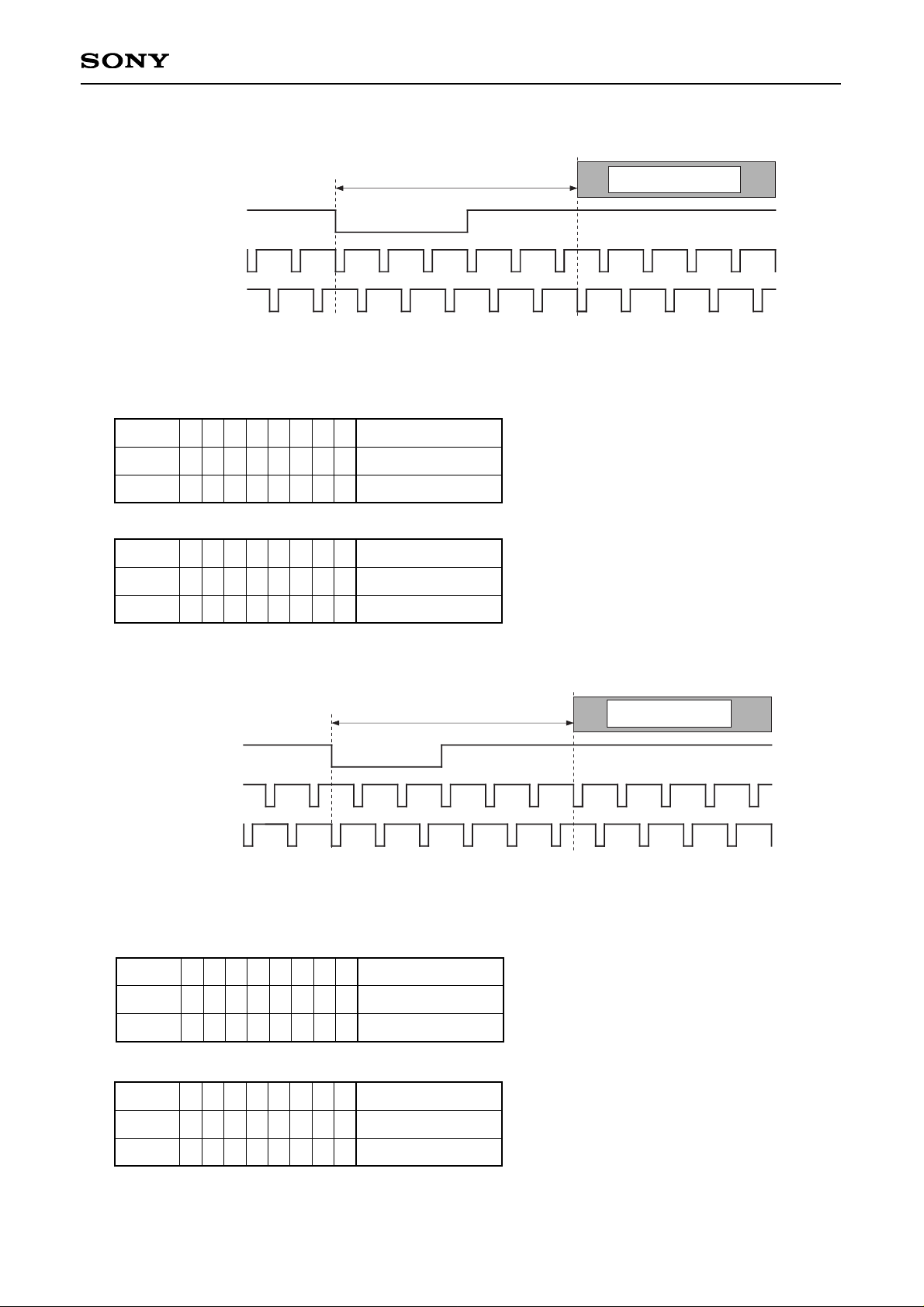
(C) VP7, 6, 5, 4, 3, 2, 1, 0
These bits set the vertical display start position. The minimum adjustment width is 1H, and adjustment of
up to 256H with 8 bits is possible using the following references.
Progressive signal input→ Front edge of VSYNC
Interlace signal input → First 1H of VSYNC
Here, the interlace signal input indicates NTSC or PAL display (using the built-in double-speed controller).
In this case, the image is raised or lowered by two lines on the panel side with respect to a 1H adjustment.
(1) Progressive
Minimum and maximum Tvp setting values
LCX026
LCX016/LCX012BL
Tvp
VSYNC
HSYNC
Image display period
Tvp: Timing from the edge of VSYNC to the start of image display
VP 7 6 5 4 3 2 1 0
Min.
Max.LH H H H H H H H 264H
L L L L L L L 9H
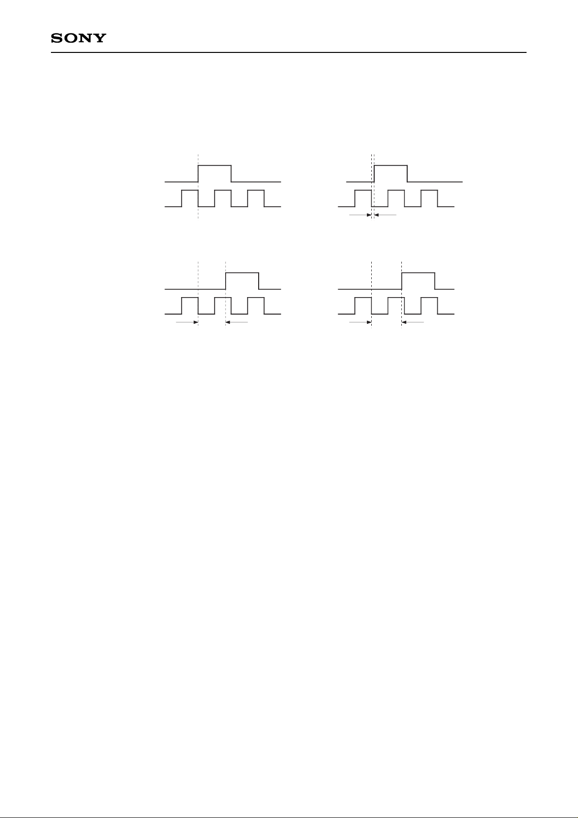
VP 7 6 5 4 3 2 1 0
Min.
Max.LH H H H H H H H 262H
L L L L L L L 7H
Page 21
– 21 –
CXD2464R
(2) Interlace
(a) NTSC
Tvp
VSYNC
HSYNC
(ODD FIELD)
HSYNC
(EVEN FIELD)
Image display period
Tvp: Timing from the edge of VSYNC to the start of image display
VP 7 6 5 4 3 2 1 0
Min.
Max.LH H H H H H H H 260.5H
L L L L L L L 5.5H
Minimum and maximum Tvp setting values
LCX026
VP 7 6 5 4 3 2 1 0
Min.
Max.LH H H H H H H H 259.5H
L L L L L L L 4.5H
LCX016/LCX012BL
VP 7 6 5 4 3 2 1 0
Min.
Max.LH H H H H H H H 259.5H
L L L L L L L 4.5H
LCX016/LCX012BL
(b) PAL
Tvp
VSYNC
HSYNC
(ODD FIELD)
HSYNC
(EVEN FIELD)
Image display period
Tvp: Timing from the edge of VSYNC to the start of image display
VP 7 6 5 4 3 2 1 0
Min.
Max.LH H H H H H H H 260.5H
L L L L L L L 5.5H
Minimum and maximum Tvp setting values
LCX026
Page 22
– 22 –
CXD2464R
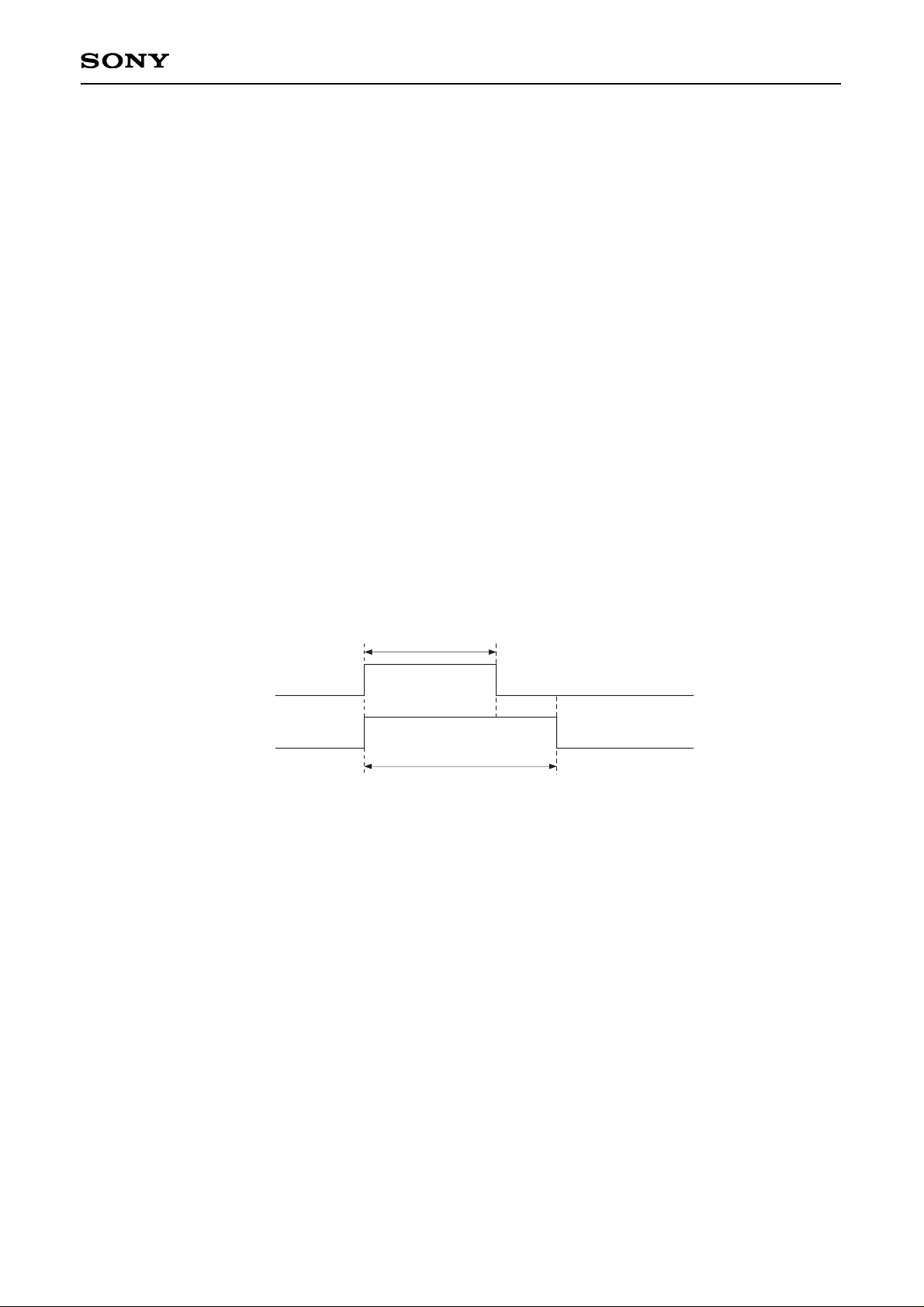
(D) HSTP3, 2, 1, 0
These bits control the HST phase relative to HCK, and correct the delay between HST and HCK that occurs
within the panel. The phase of 12 position (in 1 clk increments) can be controlled with 4 bits.
HCK1
HST
: LLLL
0
HSTP3, 2, 1, 0
: LLLH
1
1 clk (1 × 1 clk)
HCK1
HST
: HLHL 10
HSTP3, 2, 1, 0
: HLHH, HHXX
> 10
11 clk (11 × 1 clk)
10 clk (10 × 1 clk)
Notes)
1. When setting to the LCX012BL mode, the phases of HST and HCK1, 2 are as shown above regardless of
RGT.
2. In the LCX026 and LCX016 modes, when set to the SVGA mode and RGT: L or to a mode other than the
SVGA mode and RGT: H, the phase relationship between HST and HCK1, 2 is as shown above.
3. The polarity of HCK1, 2 is reversed when set to panel mode switching, panel display area switching and
right/left inversion modes other than as described in notes 1 and 2 above.
Page 23
– 23 –
CXD2464R
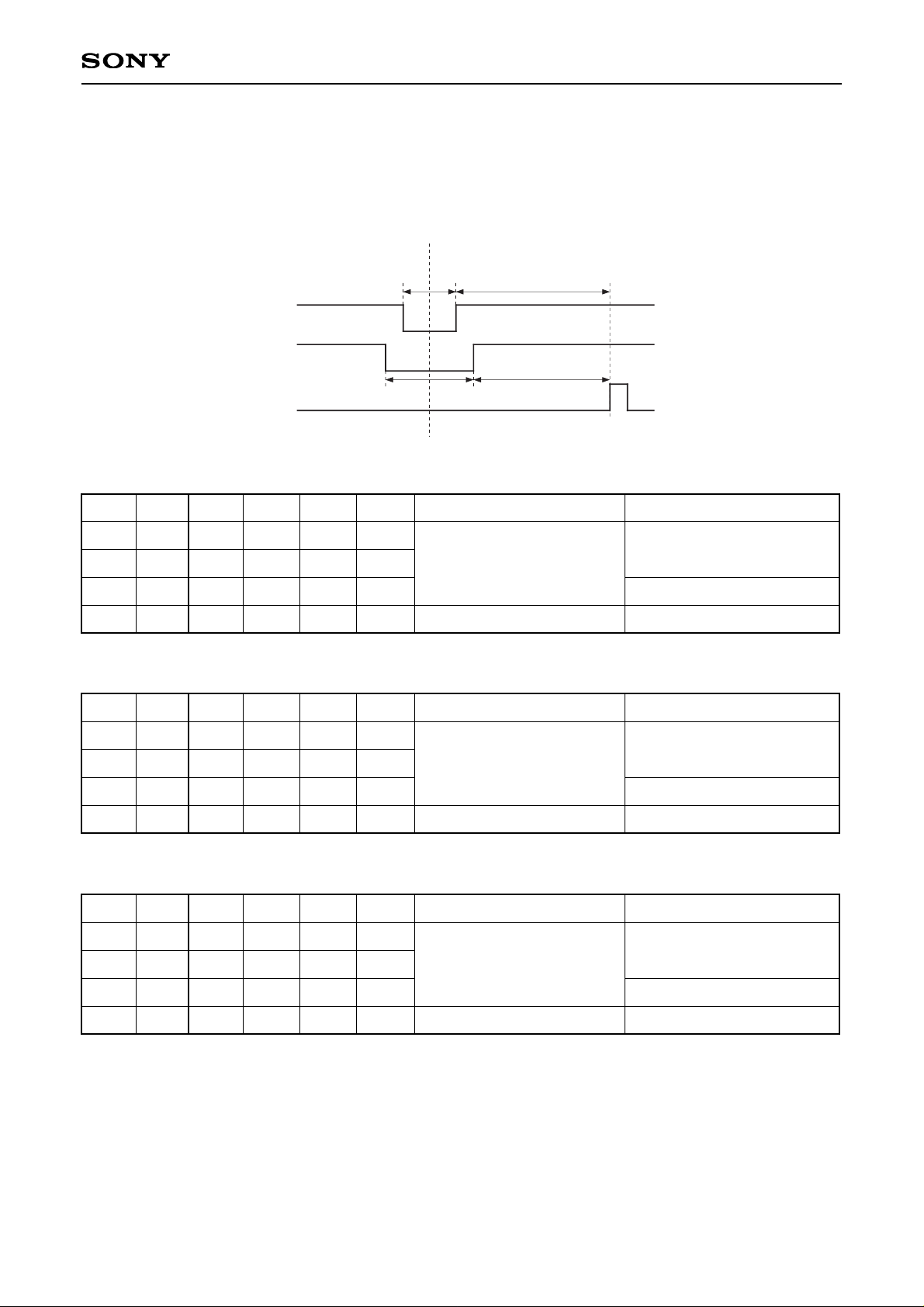
(E) PCGP4, 3, 2, 1, 0/PRGP4, 3, 2, 1, 0
These bits set the width of PCG and PRG pulses to 32 positions with 5 bits in 4 clk units.
The rise positions of PCG and PRG pulses are determined by serial data HP (see (B)), modes 1, 2 and 3 (see
(H-7)) and PCG (see (H-12)) position. The pulse widths of PCG and PRG can be arbitrarily set within the
above range using the rise positions for the reference.
When setting PCGP4, 3, 2, 1, 0 = n (decimal), the panel width at that time is calculated by:
(n + 1) × 4 (clk)
When setting PCGP4 to 0, the pulse fall position changes relative to the pulse rise position.
This applies similarly to PRGP4 to 0.
For example, when setting PCGP4, 3, 2, 1, 0: HLLHH = 19 (decimal), the panel width becomes:
(19 + 1) × 4 = 80 clk
Since the optimum values for pulse width of PCG and PRG pulses vary according to the LCD panel used, set
while also referring to the panel specifications.
Example) MCK: 50MHz (1 clk = 20ns)
PCG
: LHHHL (LSB) = 14 (decimal)
PRG
: HLHLL (LSB) = 20 (decimal)
PCGP4, 3, 2, 1, 0
PRGP4, 3, 2, 1, 0
84 clk = 1.68µs
60 clk = 1.2µs
Notes) PCGPOL and PRGPOL are both assumed to be "H".
Polarity is reversed when PCGPOL and PRGPOL are each "L".
Page 24
– 24 –
CXD2464R
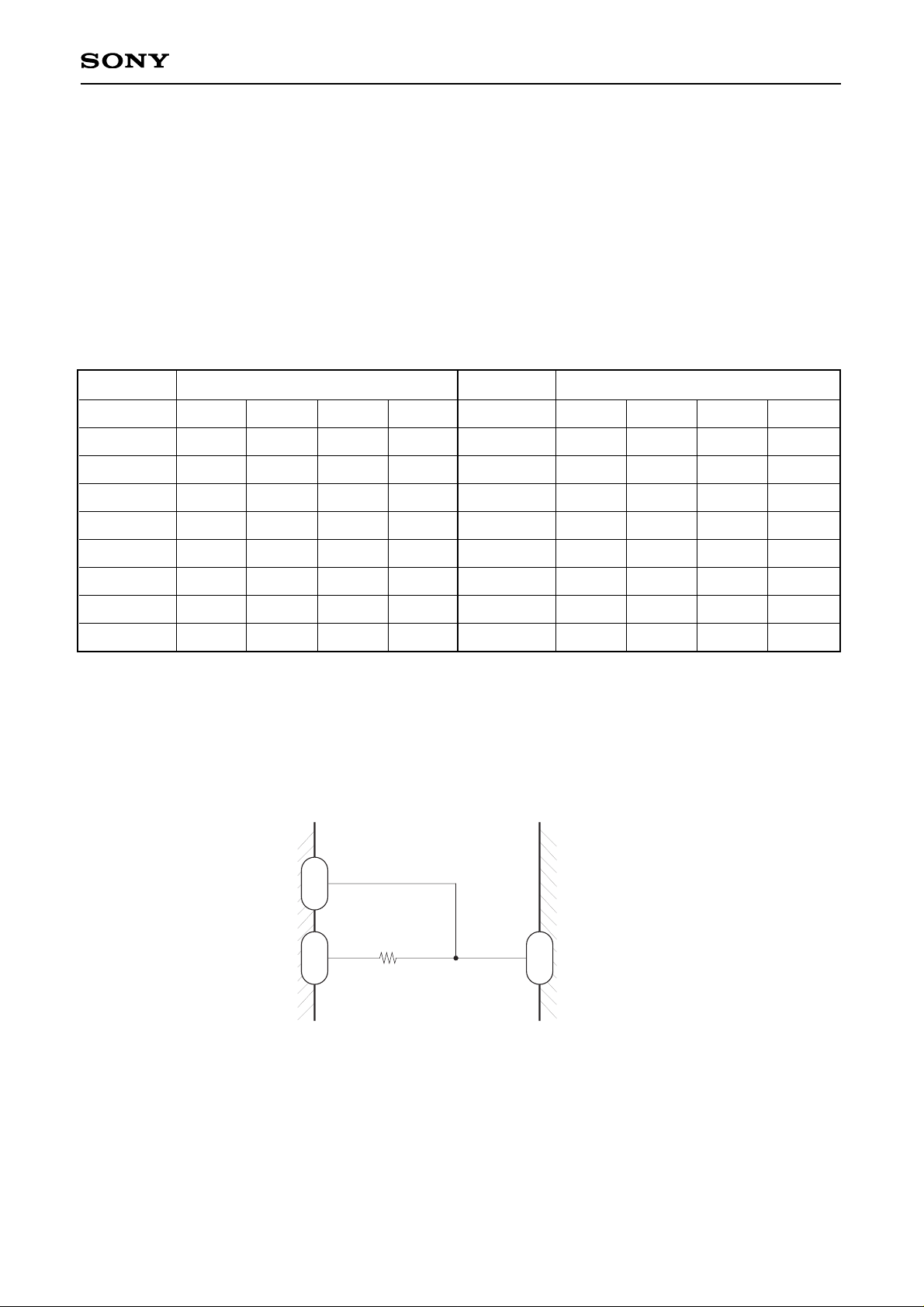
(F) CLPP1, 0
These bits adjust the clamp pulse output timing. The timing can be set to 4 positions with 2 bits.
Tclp1
Wclp1
CLP1
Tclp2
Wclp2
CLP2
HST
The centers of the CLP1 and CLP2 pulses match.
XGA (LCX026), Macintosh16 (LCX016)
CLPP1 CLPP0 Tclp1 Tclp2 Wclp1 Wclp2
L L 46 clk 23 clk 69 clk 115 clk
L
H
H
H
L
H
69 clk
92 clk
115 clk
46 clk
69 clk
92 clk
69 clk
69 clk
69 clk
115 clk
115 clk
115 clk
HP Limit (CLP2)
HHHHHHHH (255): LSB
HHHHLLHH (243): LSB
HHLHHHLL (220): LSB
HP Limit (CLP1)
HHHHHHHH (255): LSB
HHHHLLHH (243): LSB
Note) When CLPP1, 0 is set to HL or HH, the pulses may not be output due to the internal logic depending on
the HP serial data setting value. HP Limit is the upper limit for the serial data HP that allows output of
CLP1 and 2 pulses when setting each mode.
HSTP is LLHH (LSB) (serial data).
SVGA (LCX026, LCX016)
CLPP1 CLPP0 Tclp1 Tclp2 Wclp1 Wclp2
L L 38 clk 19 clk 58 clk 96 clk
L
H
H
H
L
H
57 clk
76 clk
95 clk
38 clk
57 clk
76 clk
58 clk
58 clk
58 clk
96 clk
96 clk
96 clk
HP Limit (CLP2)
HHHHHHHH (255): LSB
HHHHLHHL (246): LSB
HHHLLLHH (227): LSB
HP Limit (CLP1)
HHHHHHHH (255): LSB
HHHHLHHL (246): LSB
VGA/NTSC, PAL, PC-98 (LCX026, LCX012BL), VGA/NTSC, PAL, PC-98, WIDE (LCX016)
CLPP1 CLPP0 Tclp1 Tclp2 Wclp1 Wclp2
L L 26 clk 13 clk 38 clk 64 clk
L
H
H
H
L
H
39 clk
52 clk
65 clk
26 clk
39 clk
52 clk
38 clk
38 clk
38 clk
64 clk
64 clk
64 clk
HP Limit (CLP2)
HHHHHHHH (255): LSB
HHHHHLLL (248): LSB
HHHLHLHH (235): LSB
HP Limit (CLP1)
HHHHHHHH (255): LSB
HHHHHLLL (248): LSB
Page 25
– 25 –
CXD2464R
(G) INV, SHP3, 2, 1, 0
This IC allows control of the sample-and-hold position of the CXA2112R sample-and-hold driver by setting
serial data in place of not having a sample-and-hold pulse output.
INV set by serial data is output from the INV pin (Pin 49). Connect this INV to INV_CNT (Pin 52) of the
CXA2112R.
In addition, data set with SHP3, 2, 1, 0 is reflected in the SHPA, SHPB, SHPC and SHPD output pins (pins 45,
46, 47 and 48) as shown in the table below.
Setting
SHP3, 2, 1, 0
LLLL
LLLH
LLHL
LLHH
LHLL
LHLH
LHHL
LHHH
Output
SHPA
L
H
Z
Z
L
L
Z
Z
SHPB
L
H
L
H
L
H
L
H
SHPC
L
L
L
L
H
H
H
H
SHPD
L
L
L
L
H
H
H
H
Setting
SHP3, 2, 1, 0
HLLL
HLLH
HLHL
HLHH
HHLL
HHLH
HHHL
HHHH
Output
SHPA
L
H
Z
Z
L
L
Z
Z
SHPB
L
H
L
H
L
H
L
H
SHPC
Z
Z
Z
Z
Z
Z
Z
Z
SHPD
L
L
L
L
H
H
H
H
∗
Z: High Impedance State
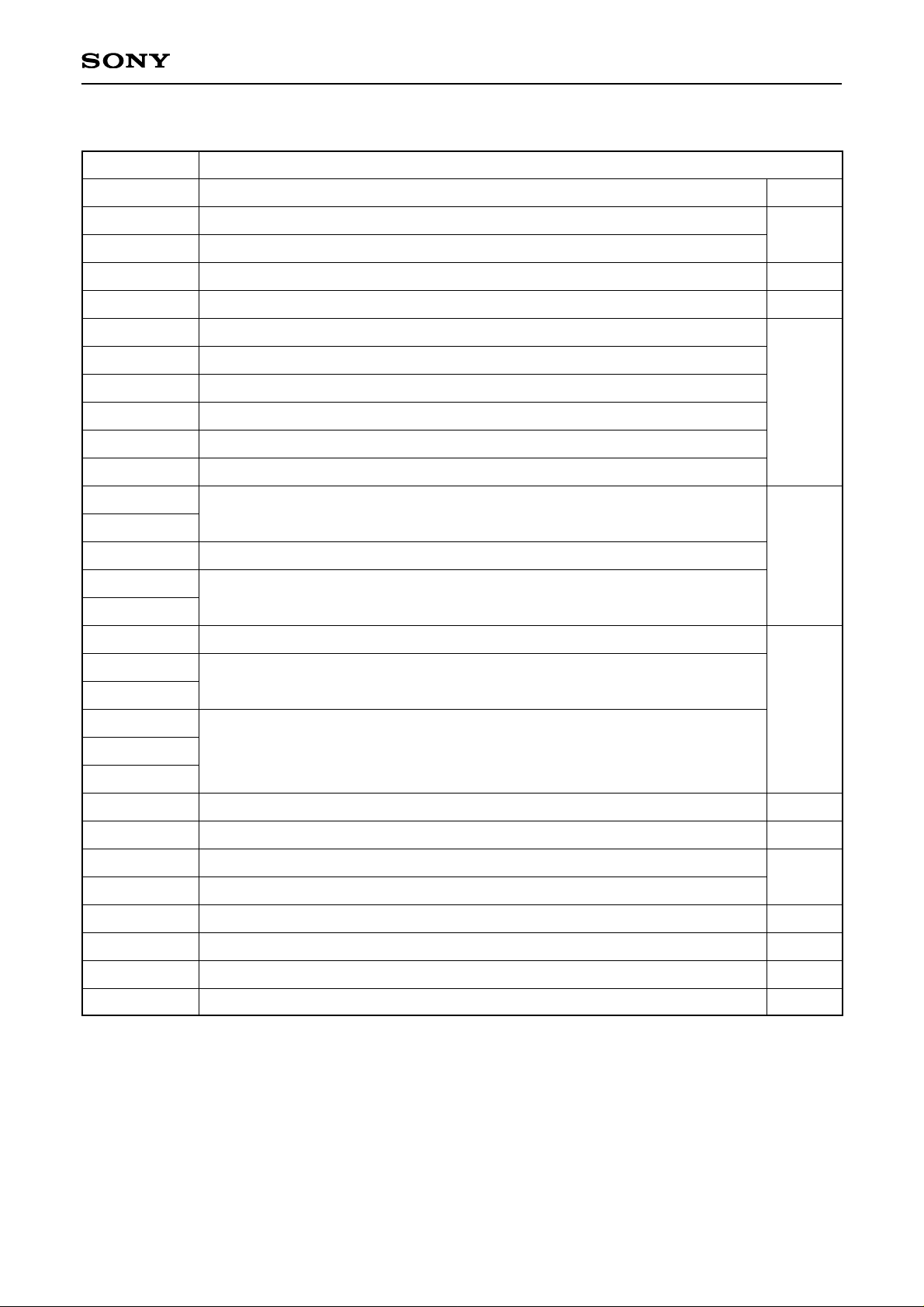
The sample-and-hold position of the CXA2112R can be set by connecting SHPA to SHPD as shown in the
diagram below. Refer to the specification of the CXA2112R for further details.
CXD2464R
SHPA (Pin 45)
(SHPC (Pin 47))
SHPB (Pin 46)
(SHPD (Pin 48))
45
(47)
46
(48)
1
(2)
POS_CNT1 (pin 1)
(POS_CNT2 (pin 2))
CXA2112R
Page 26
– 26 –
CXD2464R
(H) Mode settings
Mode
Mode description
FLD
FRP1
FRP0
CKTEST0, 1
RCK
VPOL
HPOL
HDNPOL
CLPPOL
PCGPOL
PRGPOL
MBKB
MBKA
MBK2
MBK1
MBK0
MODE021
MODEB
MODEA
MODE3
MODE2
MODE1
VGAV
HR
DWN
RGT
HST
PCG
DSP
PC98
H-1
H-2
H-3
H-4
H-5
H-6
H-7
H-8
H-9
H-10
H-11
H-12
H-13
H-14
FLD pulse output switching (H: FLD, L: CLP2)
FRP polarity inversion cycle switching (H: 1F, L: 2F)
FRP polarity inversion cycle switching (H: 1H, L: F)
Test setting (Set to H.)
Clock output setting (H: CLK STOP, L: CLK OUT)
Input VSYNC polarity switching (H: Positive, L: Negative)
Input HSYNC polarity switching (H: Positive, L: Negative)
HDN pulse output polarity switching (H: Positive, L: Negative)
CLP pulse output polarity switching (H: Positive, L: Negative)
PCG pulse output polarity switching (H: Positive, L: Negative)
PRG pulse output polarity switching (H: Positive, L: Negative)
Skip scan interval switching
Skip scan (FRP) timing switching (H: Main, L: Sub)
Skip scan mode switching (H/H: No skip scan, H/L: 6, 4 skip scan,
L/H: 5, 4 skip scan, L/L: 6, 7 skip scan)
Test setting (Set to L.)
Panel mode switching
(H/H: LCX026 mode, L/H: LCX016 mode, L/L: LCX012BL mode)
Panel display area switching
Input signal attribute switching (H: Data, L: AV)
External reset switching (H: No reset, L: Reset)
Up/down inversion discrimination signal input (H: Down, L: Up)
Right/left inversion discrimination signal input (H: Normal, L: Reverse)
HST width switching (H: 12 dots wide, L: 24 dots wide)
PCG width switching (H: Main, L: Sub)
Double-speed mode switching (H: Normal, L: Double-speed)
PC-98 (400 line) display switching (H: No display, L: Display)
Page 27

– 27 –
CXD2464R
(H-1) FLD
This bit switches the outputs of field identification pulse FLDO and clamp pulse CLP2. The FLDO pulse when
FLD is H and the CLP2 pulse when FLD is L are output from Pin 41 (CLP2/FLDO).
Refer to the timing chart for details.
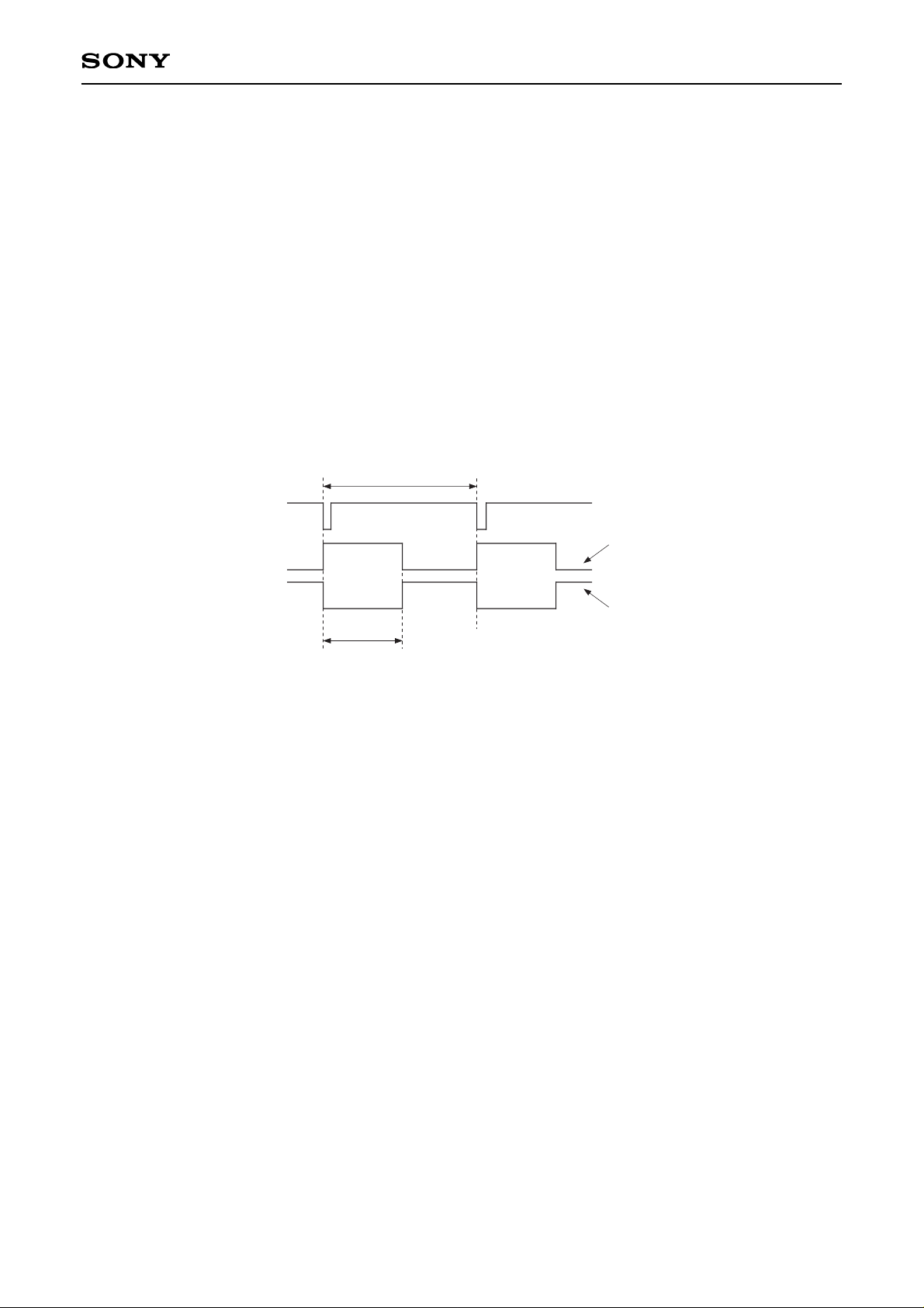
(H-2) FRP1, 0
These bits are the data for switching the LCD AC conversion signal cycle. FRP1, 0 should normally be set to HH.
FRP1, 0: HH
FRP1, 0: LH
FRP1, 0: HL
FRP1, 0: LL
1F
1H
(1F/1H inversion)
(2F/1H inversion)
(1F inversion)
(2F inversion)
(H-3) CKTST0, 1
These bits set testing. CKTST0, 1 should normally be set to H.
Note) If these bits are set to L, pulses may not be output normally.
(H-4) RCK
This bit sets testing. RCK should normally be set to H.
Page 28
– 28 –
CXD2464R
(H-5) VPOL, HPOL, HDNPOL, CLPPOL, PCGPOL, PRGPOL
These bits are the data for switching input or output signal polarity. Set these bits according to the explanation
below.
(1) VPOL and HPOL are the data for switching the input vertical and horizontal sync signal polarity. Since
signal processing is performed with the sync signal polarity fixed to positive by the internal logic, the data
must be switched according to the polarity of the input sync signal.
Therefore, individually set VPOL and HPOL to H when the polarity of the input sync signal is positive, and
to L when the polarity is negative.
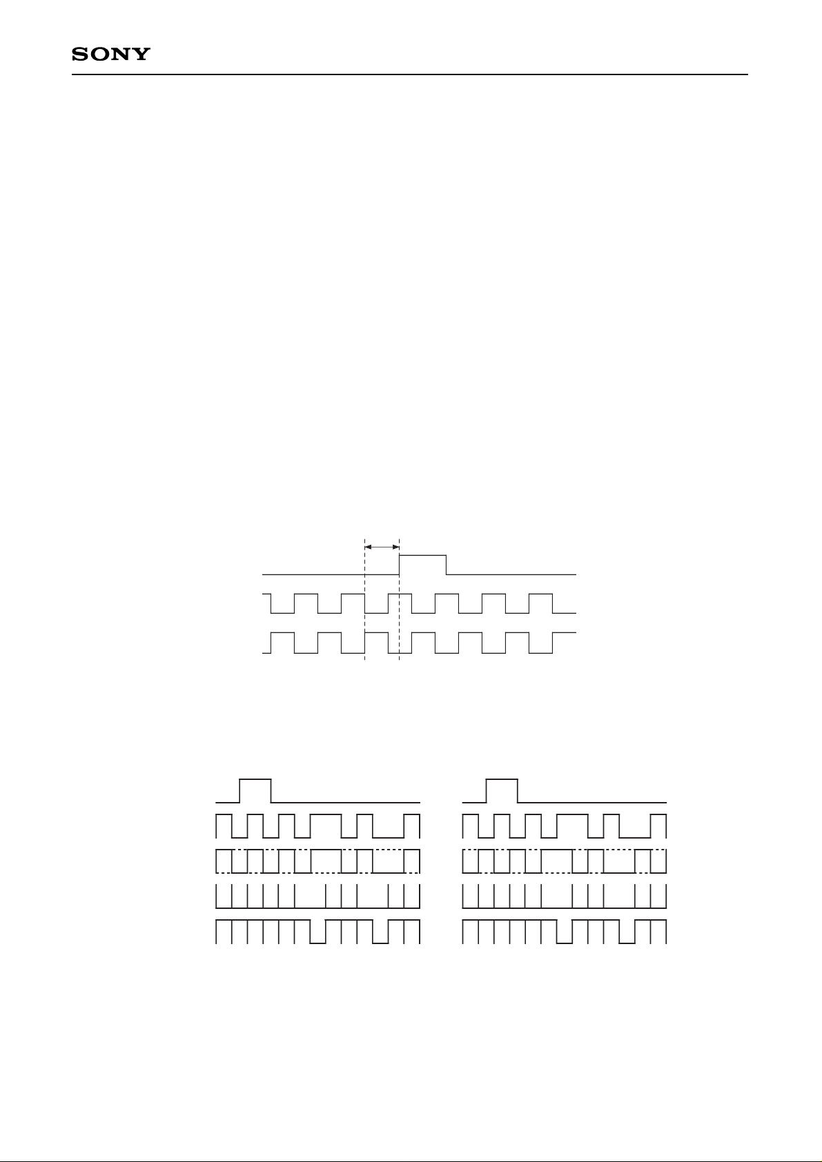
(2) The HDN pulse (H return pulse) is the 1/N frequency divider output pulse for the PLL IC. The width of the
HDN pulse is calculated according to the setting of PLLP10 to 0 for the value of frequency division N, and
that value is N/2. HDNPOL is the data for setting the output polarity of this HDN pulse, and the
relationship between its setting and pulse polarity is shown in the diagram below.
HSYNC
HDN
HPOL: L
N/2 clk
HDNPOL: L
HDNPOL: H
N clk
(3) CLPPOL sets the output polarity of clamp pulses CLP1 and CLP2. When CLPPOL is H, both CLP1 and
CLP2 have positive polarity, and when CLPPOL is L, both CLP1 and CLP2 have negative polarity.
See the Timing Charts for details.
(4) PCGPOL and PRGPOL set the output polarity for the PCG and PRG pulses, respectively. When
PCGPOL is H, the polarity of the PCG pulse is positive, and when PCGPOL is L, polarity is negative. This
applies similarly to the relationship between PRGPOL and PRG pulses.
See the Timing Charts for details.
Page 29
– 29 –
CXD2464R
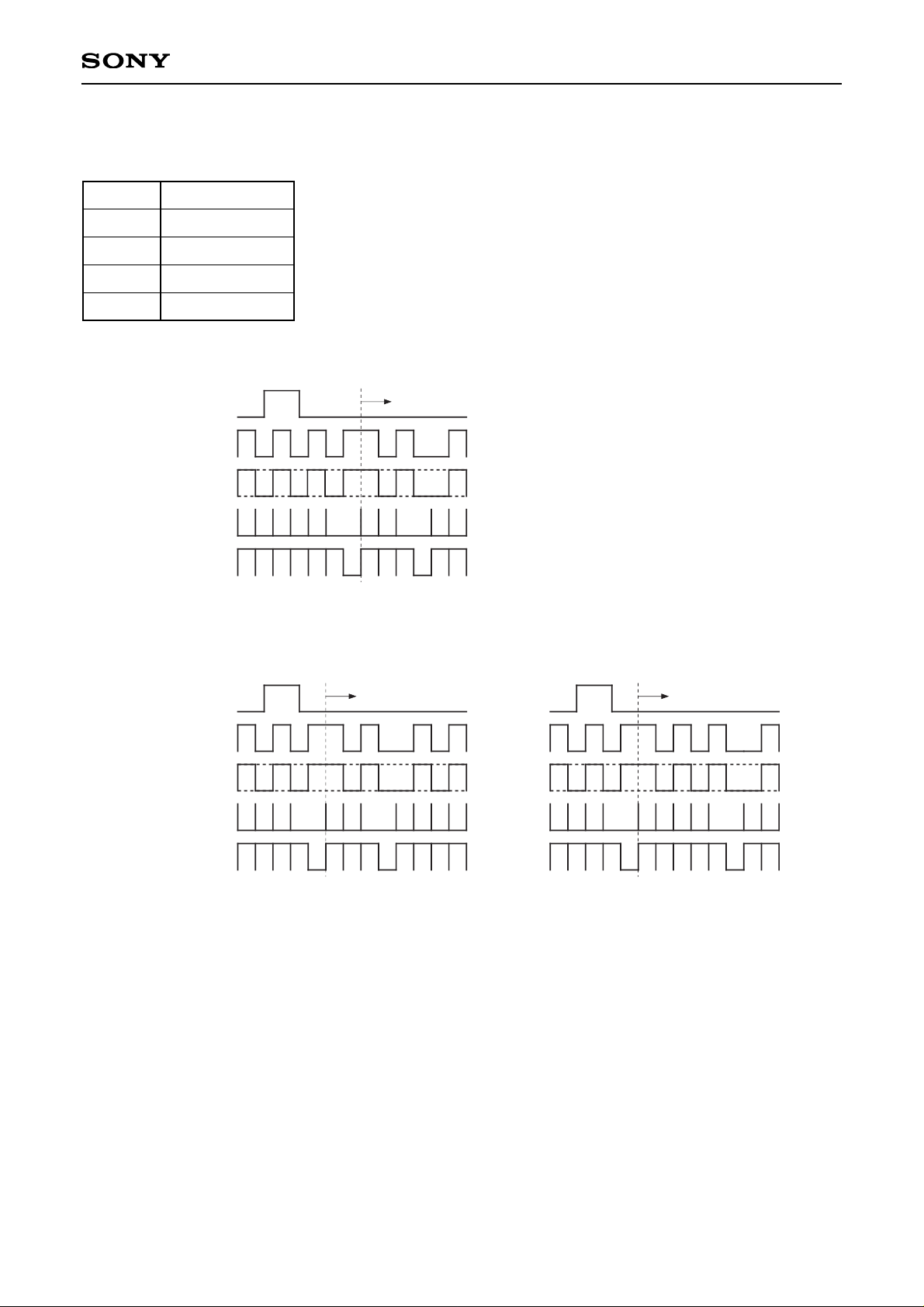
(H-6) MBK2, 1, 0, B, A
These bits set the skip-scan-related mode timings. These timings enable XGA (scanning line conversion from
768 to 598 vertical lines by 5, 4 skip scan) display for the LCX026, XGA (scanning line conversion from 768 to
615 vertical lines by 6, 4 skip scan) display for the LCX016, and SVGA (scanning line conversion from 600 to
480 vertical lines by 6, 4 skip scan) and double-speed PAL (scanning line conversion from 575 to 480 vertical
lines by 6, 7 skip scan) display for the LCX012BL. However, for XGA and SVGA display, the horizontal
direction is supported by external signal processing.
Note) Supported input signals (XGA, SVGA) differ for each panel. Use the XGA skip scan display of the
LCX026 in the XGA mode, the XGA skip scan display of the LCX016 in the Macintosh16 mode, and the
SVGA skip scan display of the LCX012BL in the VGA or SVGA mode. At that time, the display area
other than the image display area is written by the blanking level of the video signal according to the
mode.
Setting during LCX026 panel driving
When the input signal is XGA (1024 × 768), set the operation of the CXD2464R to the XGA mode of the
LCX026, and set the serial data HSTP to HSTP3/2/1/0: HLLH (LSB).
See the Timing Charts for details.
(1) MBK2
This bit sets the FRP-related skip scan timing.
9 clk
HST
HCK1
HCK2
HSTP3, 2, 1, 0: HLLH (LSB)
VST
VCK
FRP
HST/PCG
ENB
MBK2: H (MAIN) MBK2: L (SUB)
Page 30
– 30 –
CXD2464R
Note) MBK2: H and MBKB, A: LL.
MBK1, 0 Skip scan mode
LL
LH 5, 4 skip scan
HL 6, 4 skip scan
HH No skip scan
6, 7 skip scan
(2) MBK1, 0
These bits set the skip scan mode. Select the XGA, SVGA or double-speed PAL skip scan mode.
VST
VCK
FRP
HST/PCG
ENB
1 2 3 4 5 6 7
1 2 3 4 5 6 7
ODD/EVEN FIELD
VST
VCK
FRP
HST/PCG
ENB
1 2 3 4 5
Display start timing
MBK1, 0: LH (026 XGA5, 4 skip scan)
Display start timing
Display start timing
MBK1, 0: HL (016 XGA, 012BL SVGA6, 4 skip scan)
MBK1, 0: LL (012BL double-speed, PAL6, 7 skip scan)
Page 31

– 31 –
CXD2464R
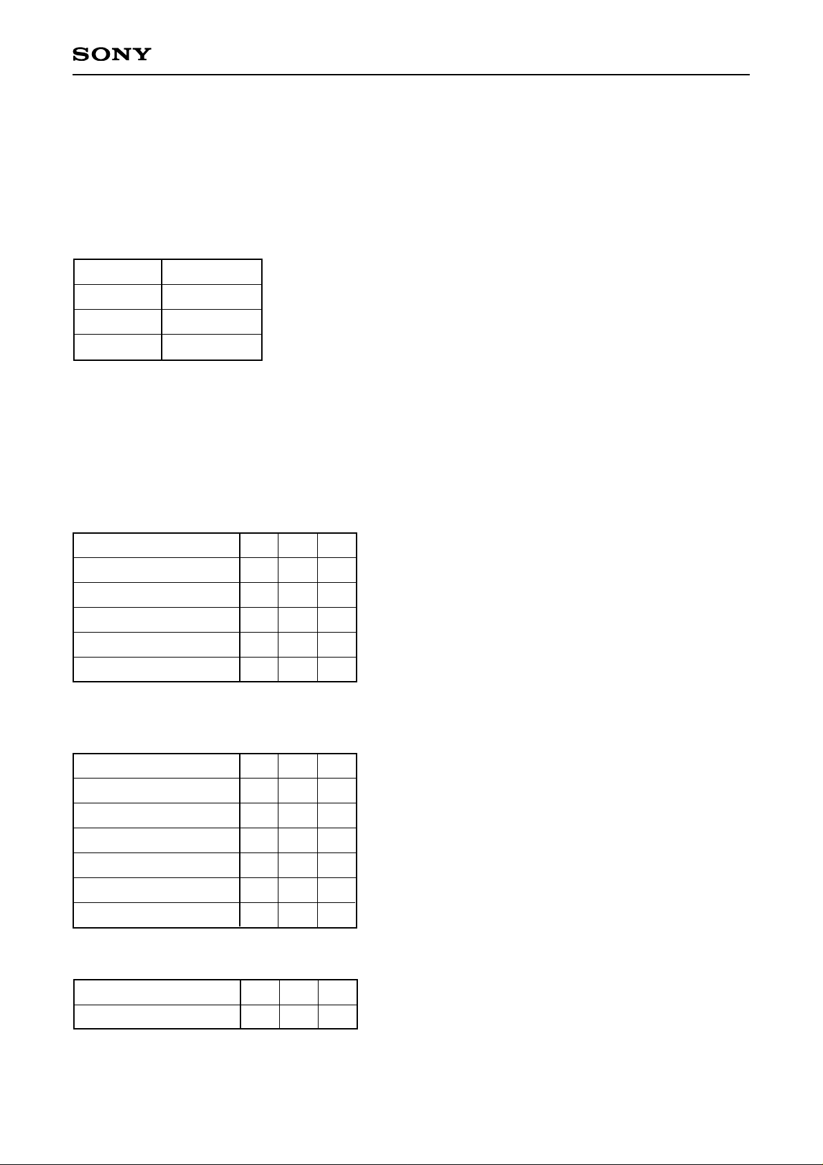
(3) MBK B, A
These bits change skip scan timing for each field (interlace) or for each V cycle (progressive). These bits
determine the skip scan timing for the next 1V period using the skip scan timing when the field identification
pulse (FLDO) is L as the reference. The optimal skip scan position can be set by setting a skip scan interval of
0 to 3H.
Although the charts below show 5, 4 skip scan timing, but the timing is the same for 6, 4 and 6, 7 skip scan.
VST
VCK
FRP
HST/PCG
ENB
1 2 3 4 5 6 7
FLDO L
VST
VCK
FRP
HST/PCG
ENB
FLDO
1 2 3 4 5 6 7
H
MBK B, A: LL
1 2 3 4 5 6 7 8
H
MBK B, A: LH
VST
VCK
FRP
HST/PCG
ENB
FLDO
1 2 3 4 5 6 7 8
H
MBK B, A: HL
1 2 3 4 5 6 7 8
H
MBK B, A: HH
Display start timing
Display start timing Display start timing
Display start timing Display start timing
Reference timing
Note) MBK2: H, MBK1, 0: LH
Page 32
– 32 –
CXD2464R
MODE 1 2 3
XGA (804 × 604)
SVGA (804 × 604)
PAL (762 × 572)
VGA/NTSC (644 × 484)
PC-98 (644 × 404)
L
L
L
L
H
L
L
H
H
L
L
H
L
H
L
MODE 1 2 3
Macintosh16 (832 × 624)
SVGA (800 × 600)
PAL (762 × 572)
VGA/NTSC (640 × 480)
PC-98 (640 × 400)
WIDE (832 × 480)
L
L
L
L
H
H
L
L
H
H
L
L
L
H
L
H
L
H
When using the LCX016
MODE 1 2 3
VGA/NTSC (644 × 484)
L H H
∗
Also supports PAL display.
MODE B, A Panel
LL
LH LCX016
HH LCX026
LCX012BL
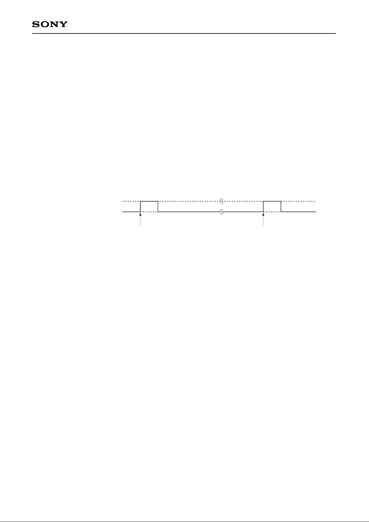
(H-7) MODE021
These bits are a test mode. MODE021 should normally be set to L.
(1) MODE B, A
These bits switch each timing according to the mode. Operation shifts to LCX026 mode when MBKB, A is HH,
to LCX016 mode when LH, and to LCX012BL mode when LL. Be sure to set this data when using the
CXD2464R in these modes.
(2) MODE3, 2, 1
These bits switch the panel display area. However, since the panel display area cannot be switched for the
LCX012BL, VGA/NTSC mode should be set when using the LCX012BL.
In addition, set to the XGA mode during XGA skip scan display using the LCX026, and to the Macintosh16
mode during XGA skip scan display using the LCX016.
When using the LCX026
∗
XGA skip scan display
When using the LCX012BL
Page 33
– 33 –
CXD2464R
(H-8) VGAV
This bit switches the CXD2464R according to the attributes of the input signal. The CXD2464R supports input
of data signals when VGAV is set to H, and input of interlaced video signals when set to L. Only the doublespeed NTSC, PAL and WIDE (LCX016 only) modes are supported, when using the built-in double-speed
controller. Set VGAV to L during input of these signals.
(H-9) HR
This bit controls the input horizontal sync signal (HSYNC)-based PLL counter reset operation, and supports
external clock input. (Reset operation is allowed when HR is L.)
Resetting the internal PLL counter at the front edge of the input HSYNC generates an output pulse
synchronized to HSYNC.
This function should be used with systems which do not use a PLL.
In addition, set the PLL frequency division ratio (1/N) resulting from the use of this mode according to:
Number of clk for the horizontal period – 2 = Actual number of clk set
(see page 16).
Input horizontal sync signal
(HSYNC)
Reset the internal PLL counter at this timing.
HPOL: H
Note) Since H-POSITION specifications described in this data sheet are not satisfied due to the configuration
of the internal logic, the screen center must be adjusted each time.
(H-10) DWN, RGT
These bits set the up/down and right/left inversion discrimination data. These settings allow display to be
performed in accordance with each display system.
See the Timing Charts for details.
(H-11) HST
This bit adjusts the HST width. HST should normally be set to H.
Page 34

– 34 –
CXD2464R
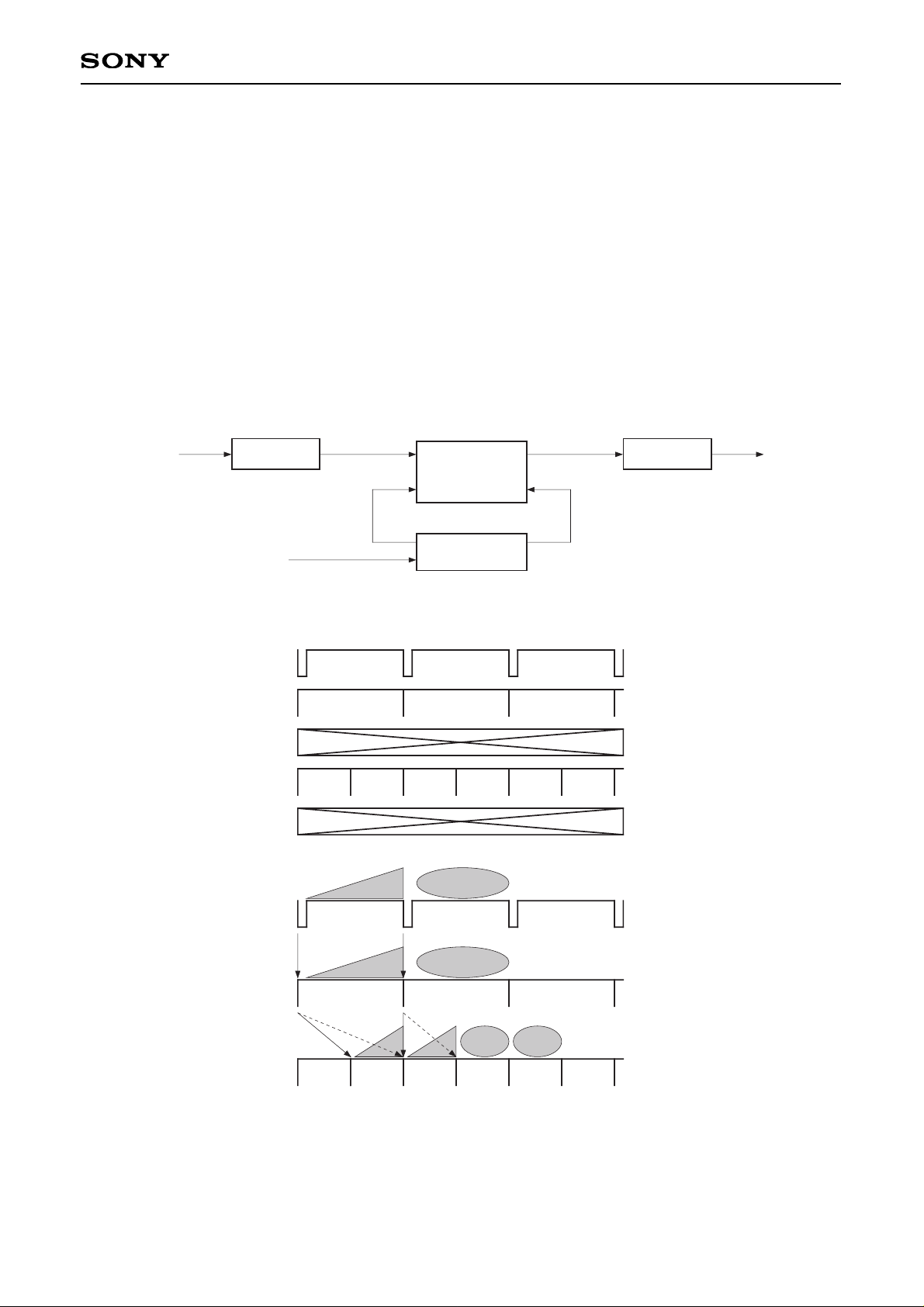
(H-12) PCG
This bit adjusts the rise (fall) position (pulse starting timing) of the PCG pulse using VCK as a reference. This
is linked with PRG and FRP.
Timing at that time. PCG should normally be set to H.
Tm
VCK
PRG
PCG
FRP
MODE
Tm Tm
XGA, Macintosh16
SVGA
PAL
VGA/NTSC
PC-98
WIDE
57 clk
48 clk
32 clk
46 clk
38 clk
26 clk
PCG = H PCG = L
Note) PCGPOL: H, PRGPOL: H
Tm value for each mode
Page 35
– 35 –
CXD2464R
(H-13) DSP
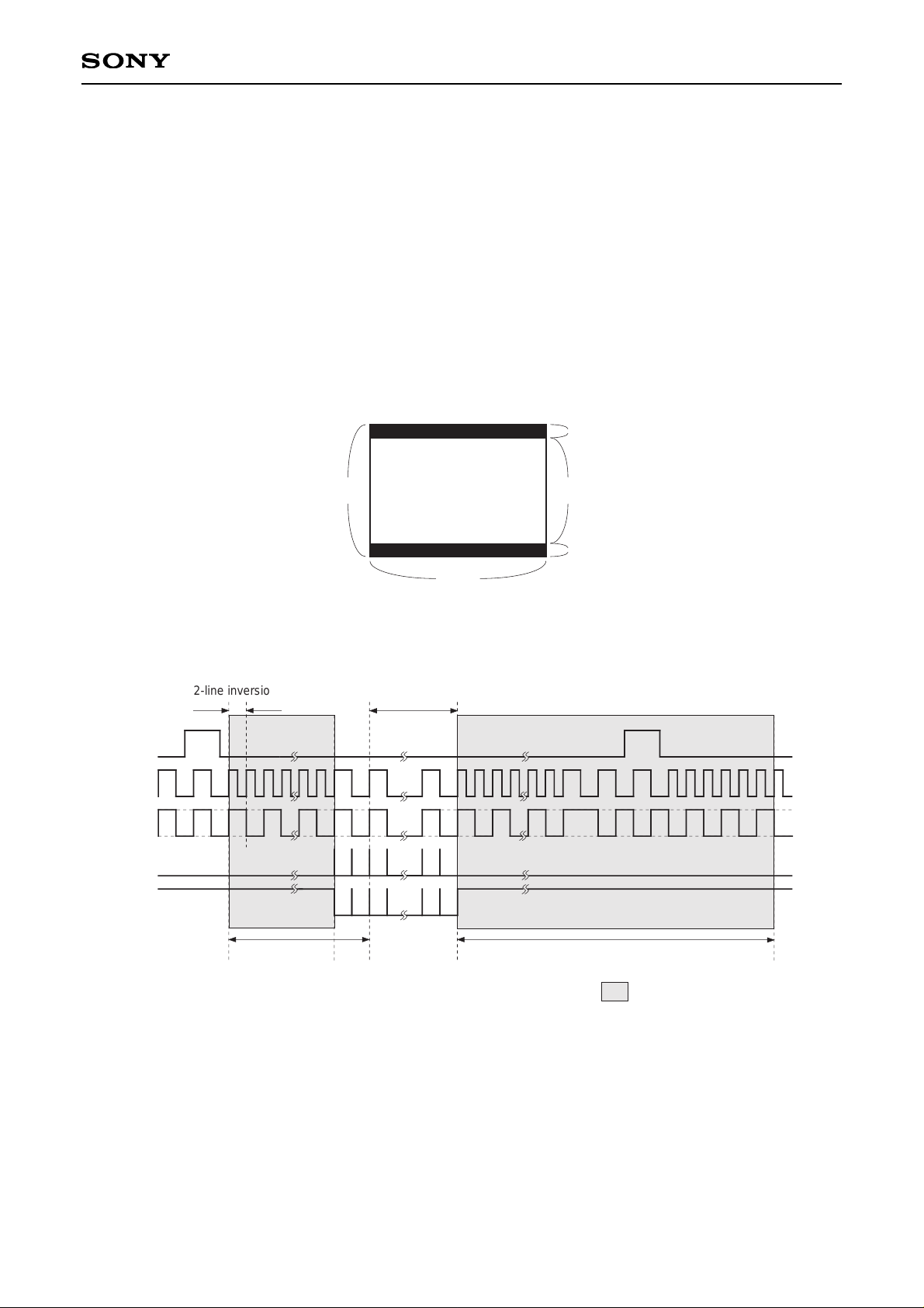
This bit performs the double-speed display mode switching settings. Operation shifts to double-speed display
mode when DSP is L. However, DSP should be set H for other modes.
This function is only supported when the built-in double-speed controller is used. This controller is designed to
use the µPD485505 (NEC/high-speed line buffer) as the system line memory IC, and generates the doublespeed processing pulses RSTW (reset write), WCK (write clock), RSTR (reset read) and RCK (read clock).
The operation of the µPD485505 is as follows. Write operation is started at the RSTW timing, and this memory
data is read at double speed at the RSTR timing which is delayed by 1/2H from the RSTW timing. Labeling the
master clock frequency (MCK) as f, the write and read clock frequencies at this time are expressed as f/2 and f,
respectively.
However, the master clock should have a frequency of 33.3MHz or less when using this mode.
See the IC specifications for a detailed description of µPD485505 operation.
Note) See the Timing Charts for details.
ADC
LINE Mem.
µPD485505
CXD2464R
DAC
RSTR
RCK
MCK: f
RSTW
WCK
R, G, B IN
HSYNC
VSYNC
HSYNC
RSTW
WCK
RSTR
RCK
f/2
f
HSYNC
RSTW
RSTR
Double-speed display system diagram
Double-speed display timing
Page 36
– 36 –
CXD2464R
(H-14) PC-98
This bit switches the PC-98 (400-vertical line) display mode. Operation shifts to PC-98 mode when PC98 is L.
However, since this function supports the LCX012BL, PC98 is normally (modes other than LCX012BL/PC-98
mode) set H.
This function is used to display PC-98 (640 × 400) images in the display area of the LCX012BL (644 × 484).
The upper and lower 42 lines outside of the display area are black display during this mode.
The vertical high-speed scanning and precharge black writing methods have been introduced as methods for
writing these black areas. VCK is shifted to double-speed operation to realize vertical double-speed transfer
and enable black display within the limited V blanking. Also, the black level during this period is determined by
the PSIG (LCX012BL) level and written at the PCG (LCX012BL) timing.
At this time, HST is masked, limiting the video signal input.
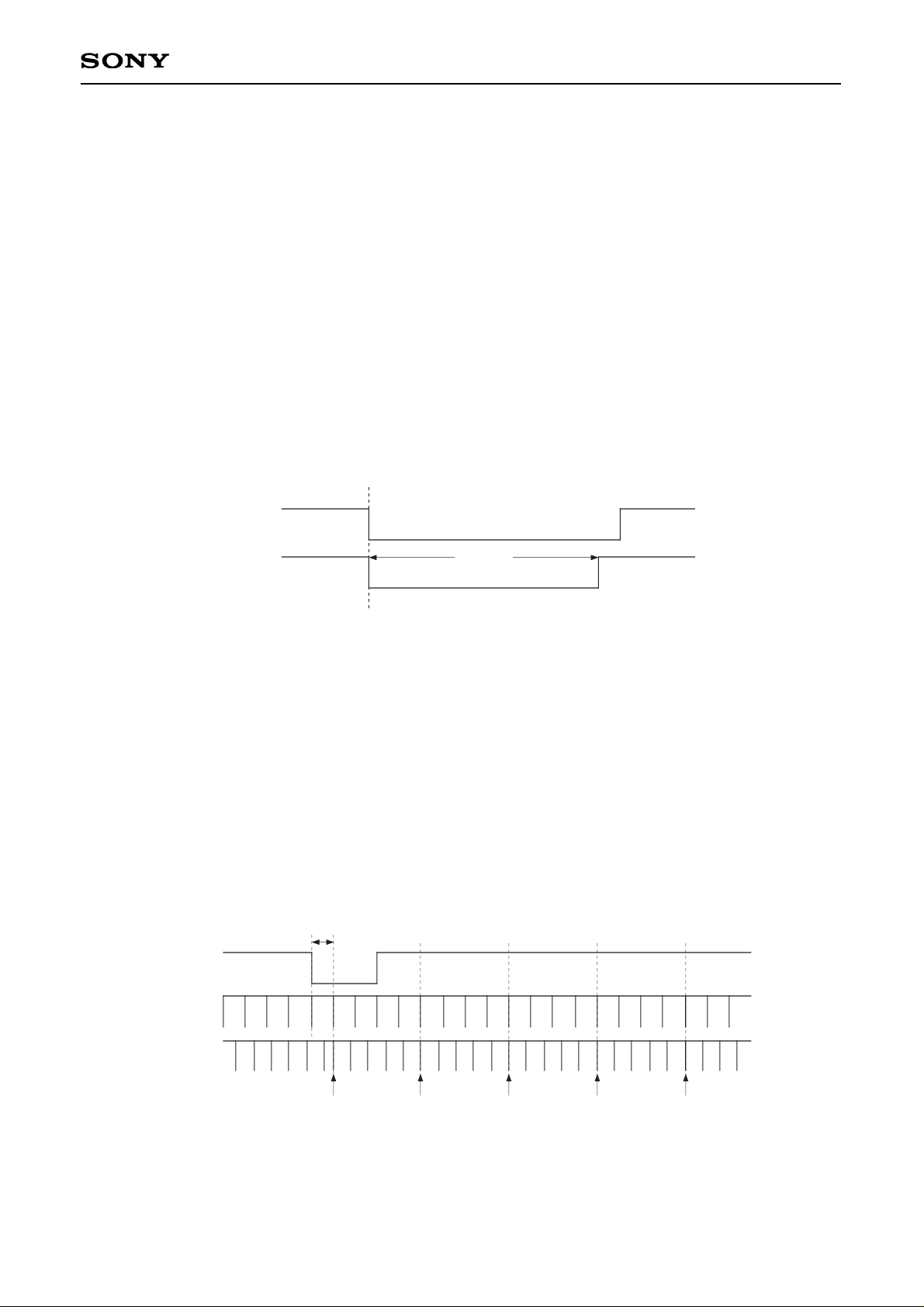
42 (A)
400 (B)
42 (C)
484
644
Effective display area
(400 lines)
Unit: dot
VST
FRP
VCK
PCG
HST
(A)
(C)
2-line inversion (FRP) Effective display area (B)
: Black frame display areas
LCX012BL panel
PC-98/400-line display timing
Note) FRP is inverted every two lines during double-speed scanning.
See the Timing Charts for details.
Page 37
– 37 –
CXD2464R
(I) to (L) Scan converter pulse settings
The following settings are not required when not using the scan converter or digital signal driver CXD2449Q.
(I-1) SLLAP
SLLAP is used when converting the number of pixels using the scan converter, when the clock differs between
input signals and output signals, etc.
SLLAP should be L during the normal operating mode.
SLLAP should be H when operating with CKI1 synchronized only with input signals of the internal circuits of the
IC, serial interface, PLL counter and phase comparator, and other components are operated with CKI2.
(I-2) IRD10 to 0, IRU10 to 0
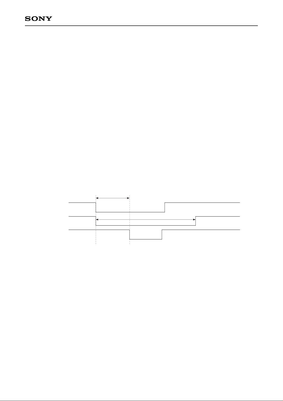
IRACT is an output pulse in sync with input HSYNC at an arbitrary position and width. Set the pulse fall
position for IRD10 (MSB) to IRD0 (LSB), and the pulse rise position for IRU10 (MSB) to IRU0 (LSB). The
setting range is from 0 to N – 1. In addition, do not set IRD and IRU to the same value.
HSYNC
IRACT
128 clk
IRD: LLLLLLLLLLL (LSB), IRU: LLLHLLLLLLL (LSB), HR: H
(J-1) ORRS3, 2, 1, 0
When SLLAP is set L, ORACT pulse is completely identical to IRACT pulse when serial data SLLAP is L, and
when SLLAP is set H, this is generated from a dedicated counter (loop counter similar to the PLL counter, and
referred to as an OR counter) that operates by CKI2, an asynchronous clock that is independent from the input
signal. In addition, pulses for LCD panel driving are also generated at this time based on the output of this
counter, enabling the LCD panel to be driven with a horizontal cycle and clock that differ from the input signal.
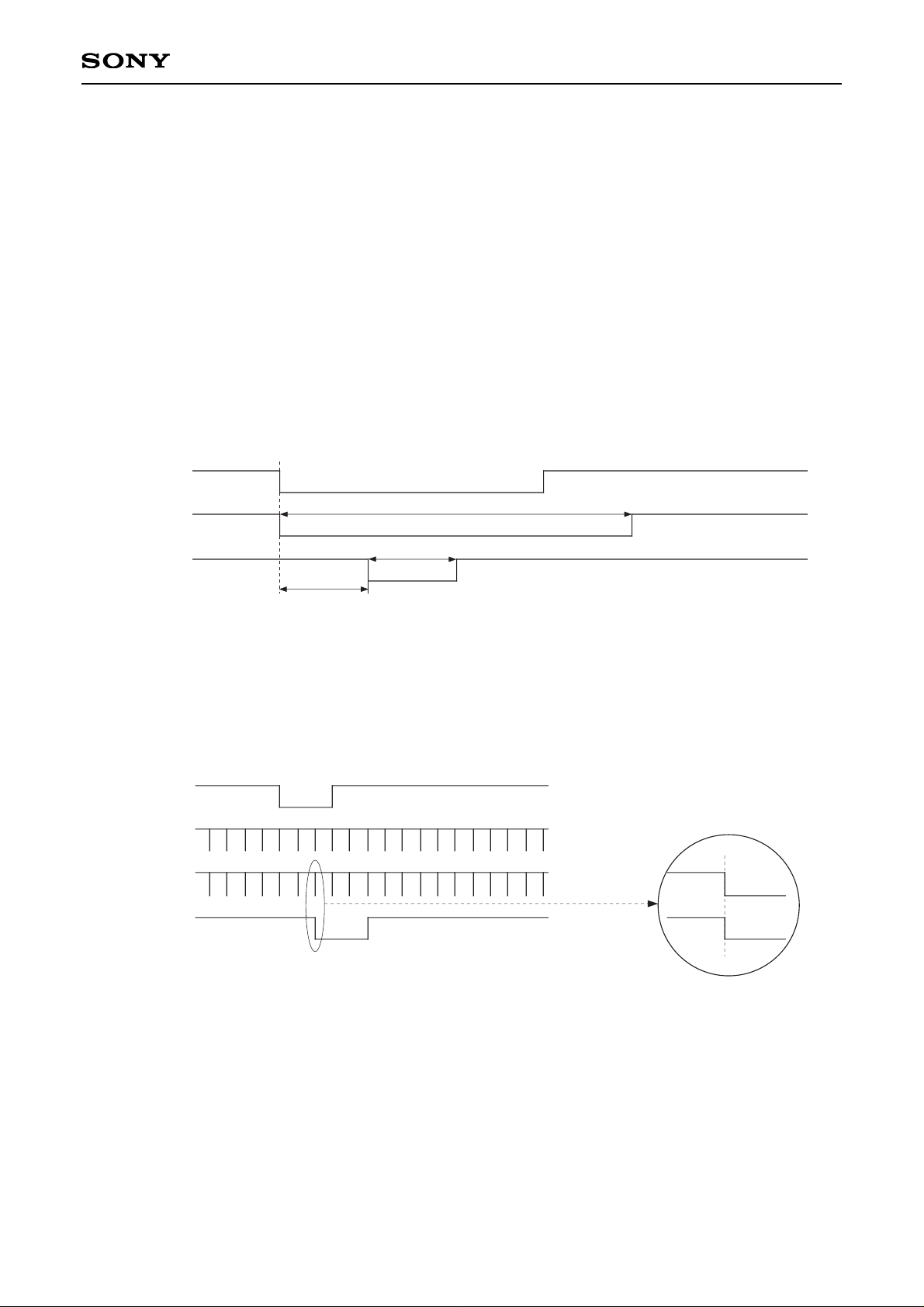
The above OR counter applies a reset with VSYNC and a fixed cycle input HSYNC in order to be in sync with
input HSYNC. ORRS3, 2, 1, 0 perform this reset by HSYNC every H seconds or a cycle is set. When ORRS3,
2, 1, 0 (LSB) are set to LLLL, reset is applied for 16H cycles, and at the set number of cycles when set to other
settings. Reset can be applied from 1H to a maximum of 16H cycles.
VSYNC
IRACT
1H
ORACT
SLLAP: H, ORRS: LHLL (LSB)
Timing by which reset is applied to OR counter
Page 38
– 38 –
CXD2464R
(J-2) ORP10 to 0
ORP sets the number of frequency divisions of the OR counter described above. Similar to PLLP10 to 0, up to
2048 divisions can be set with 11 bits of data. Set the actual number of frequency divisions M as follows:
M – 2 = actual number of clk set
(K) ORD10 to 0, ORU10 to 0
ORACT pulses can be output at an arbitrary position and width of the OR counter operated by clock CKI2 that
is asynchronous with input HSYNC when serial data SLLAP is set H.
Set the pulse fall position for ORD10 (MSB) to ORD0 (LSB), and the pulse rise position for ORU10 (MSB) to
ORU0 (LSB). The setting range is from 0 to M – 1. In addition, similar to IRACT, do not set ORD and ORU to
the same value.
As previously mentioned, when serial data SLLAP is L, ORACT pulses are identical to IRACT pulses
regardless of the settings for serial data ORU and ORD.
(L) HPRS10 to 0
Although the counter (H position counter) that generates horizontal display pulses is normally reset based on
the PLL counter, when serial data SLLAP is H, reset can be applied to the horizontal direction display counter
at an arbitrary position according to an 11-bit setting HPRS based on the OR counter. Consequently, the
horizontal display starting position can be varied over a wide range. Setting of serial data HP7 to 0 becomes
valid at this time.
ORD: LLLLLLLLLLL (LSB), ORU: LLLHLLLLLLL (LSB), HP: HHHHHHHH (LSB)
HPRS: LLLLLHHLLLL (LSB), SLLAP: H
HSYNC
ORACT
ENB
49 clk
128 clk
HSYNC when reset is applied to OR counter
Page 39

– 39 –
CXD2464R
(M) PRE
This bit sets preset.
Internal preset is reflected in the output when PRE is set L, and serial data settings are reflected in the output
when PRE is set H. When the power is turned on, all internal systems are reset, and serial data PRE is set L.
Namely, the CXD2464R is in the preset setting status. Always make sure to make all necessary settings
before canceling this status (by setting PRE H). If serial data PRE is set H before making all required serial
settings, all serial data that has not been set is set L.
When serial settings have been changed when PRE is set H, those settings are immediately reflected in the
output.
After XCLR (system reset) Pin 19 is set L to reset the system, serial data PRE is set L and the CXD2464R
enters preset setting status even after the power has been turned on. Make all required settings similar to
when turning on the power after XCLR has been set H.
The preset setting is VESA SVGA72 (horizontal frequency: 48.08kHz, vertical frequency: 72.19Hz, dot clock:
50.00MHz). Detailed setting values are as shown below.
Address Data
MSB LSB
0 0 0 0 0 0 0 0 PLLP10 to 8: HLL (LSB)
0 0 0 0 0 0 0 1 PLLP7 to 0: LLLLHHHL (LSB)
0 0 0 0 0 0 1 0 HP7 to 0: HHHLHLLH (LSB)
0 0 0 0 0 0 1 1 VP7 to 0: LLLHLLHL (LSB)
0 0 0 0 0 1 0 0 HSTP3 to 0: LLLH (LSB)
0 0 0 0 0 1 0 1 PCGP4 to 0: LHHHL (LSB)
0 0 0 0 0 1 1 0 PRGP4 to 0: HLHLL (LSB)
0 0 0 0 0 1 1 1 CLPP1 to 0: LL (LSB)
0 0 0 0 1 0 0 0 INV: L, SHP3 to 0: LLLL (LSB)
0 0 0 0 1 0 0 1 FLD: L, FRP1 to 0: HH (LSB), CKTST: H, RCK: H
0 0 0 0 1 0 1 0 VPOL: H, HPOL: H, HDNPOL: H, CLPPOL: H, PCGPOL: H, PRGPOL: H
0 0 0 0 1 0 1 1 MBKB, A: LL, MBK2, 1, 0: HHH
0 0 0 0 1 1 0 0 MODE021: L, MODEB, A: HH, MODE3, 2, 1: HLL
0 0 0 0 1 1 0 1 VGAV: H, HR: L, DWN: H, RGT: H, HST: H, PCG: H, DSP: H, PC98: H
0 0 0 1 0 0 0 0 SLLAP: L, IRD10 to 8: LLL (LSB)
0 0 0 1 0 0 0 1 IRD7 to 0: LLLLLLLL (LSB)
0 0 0 1 0 0 1 0 IRU10 to 8: LLL (LSB)
0 0 0 1 0 0 1 1 IRU7 to 0: HLLLLLLL (LSB)
0 0 0 1 0 1 0 0 ORRS3 to 0: LLLH (LSB), ORP10 to 8: LHH (LSB)
0 0 0 1 0 1 0 1 ORP7 to 0: HHHLLHHL (LSB)
0 0 0 1 0 1 1 0 ORD10 to 8: LLL (LSB)
0 0 0 1 0 1 1 1 ORD7 to 0: LLLLLLLL (LSB)
0 0 0 1 1 0 0 0 ORU10 to 8: LLL (LSB)
0 0 0 1 1 0 0 1 ORU7 to 0: HLLLLLLL (LSB)
0 0 0 1 1 0 1 0 HPRS10 to 8: LLL (LSB)
0 0 0 1 1 0 1 1 HPRS7 to 0: LLLLLLLL (LSB)
0 0 0 1 1 1 0 0 PRE: L
Page 40
– 40 –
CXD2464R
XHS and XVS Pulses
Introduction
XHS and XVS pulses are pulses for digital signal driver CXD2449Q sync signal input. XHS and XVS do not
support systems using the built-in double-speed controller. Use the double-speed scan converter (CXD2428Q)
with the CXD2449Q during NTSC or PAL double-speed display.
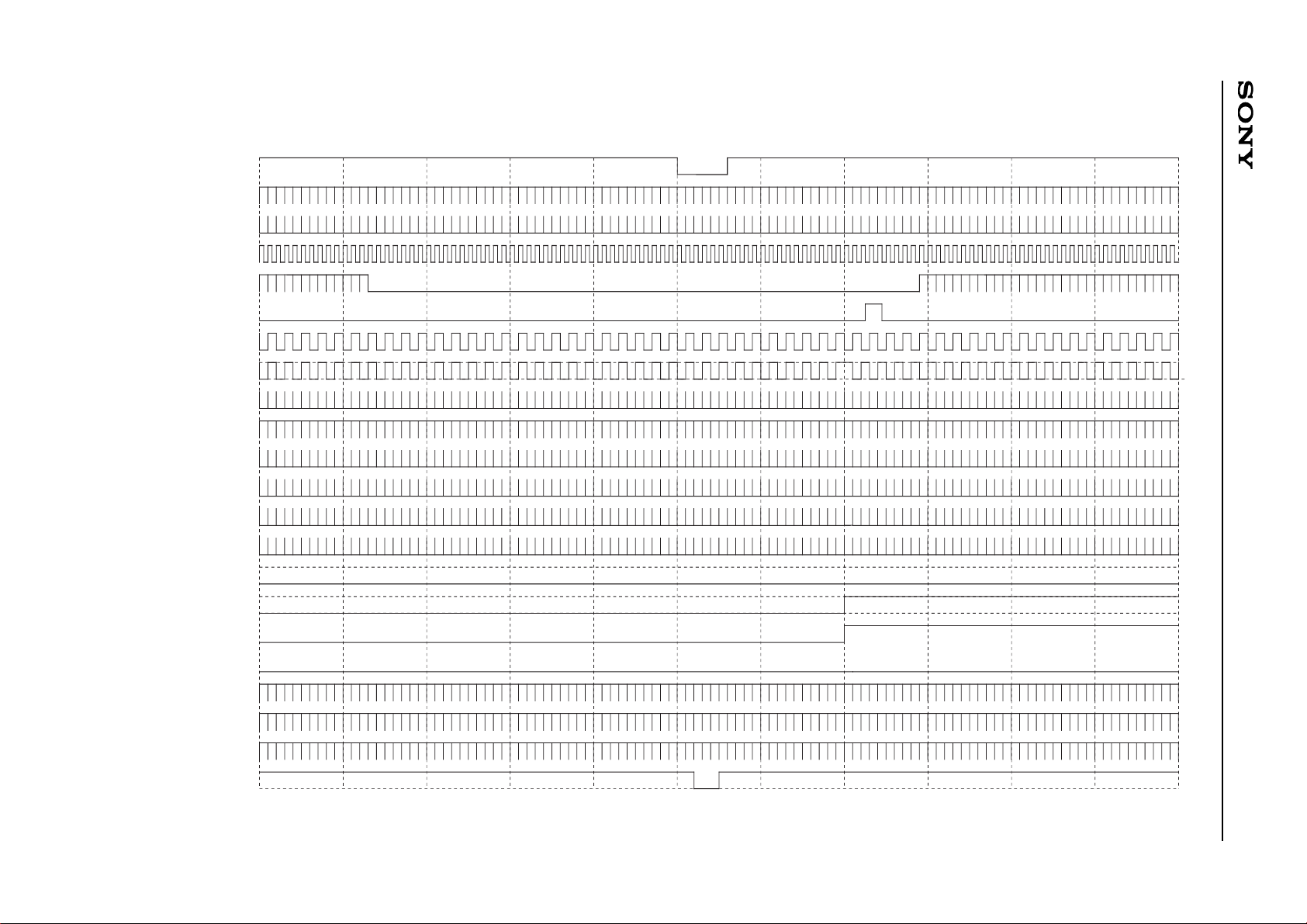
XHS pulses
XHS pulses are output with negative polarity in 32 clock widths 34 clocks after the fall of the IRACT pulse when
serial data SLLAP is L. Similarly, XHS pulses are output with negative polarity in 32 clock widths 34 clocks
after the fall of the ORACT pulse when serial data SLLAP is H. Therefore, in order to output XHS pulses
correctly, respectively set serial data IRD10 to 0 and IRU10 to 0 when serial data SLLAP is L, and ORD10 to 0
and ORU10 to 0 when serial data SLLAP is H.
HSYNC
ORACT
XHS
ORD10 to 0: LLLLLLLLLLL, ORU10 to 0: LLLHLLLLLL
34 clk
32 clk
128 clk
XVS pulses
XVS pulses are output with negative polarity in 3H widths 2H after the vertical sync signal. The phase
relationship between XHS and XVS pulses at this time is as shown in the diagram below.
VSYNC
HSYNC
XVS
XHS
Note) XHS and XVS pulses output ENB and BLK pulses (negative polarity), respectively, for the sake of
convenience when using the built-in double-speed controller.
Page 41
– 41 –
CXD2464R
MODE3/2/1 : H/L/L MODE B/A : H/H MODE021 : L DWN : H VP : LLLHLLHL (LSB) MBK2/1/0/B/A : H/H/H/L/L FRP1/0 : H/H VPOL : L VGAV : H PC98 : H
12
VSYNC
HSYNC
HD
HDN
(BLK)
VST
VCK
FRP
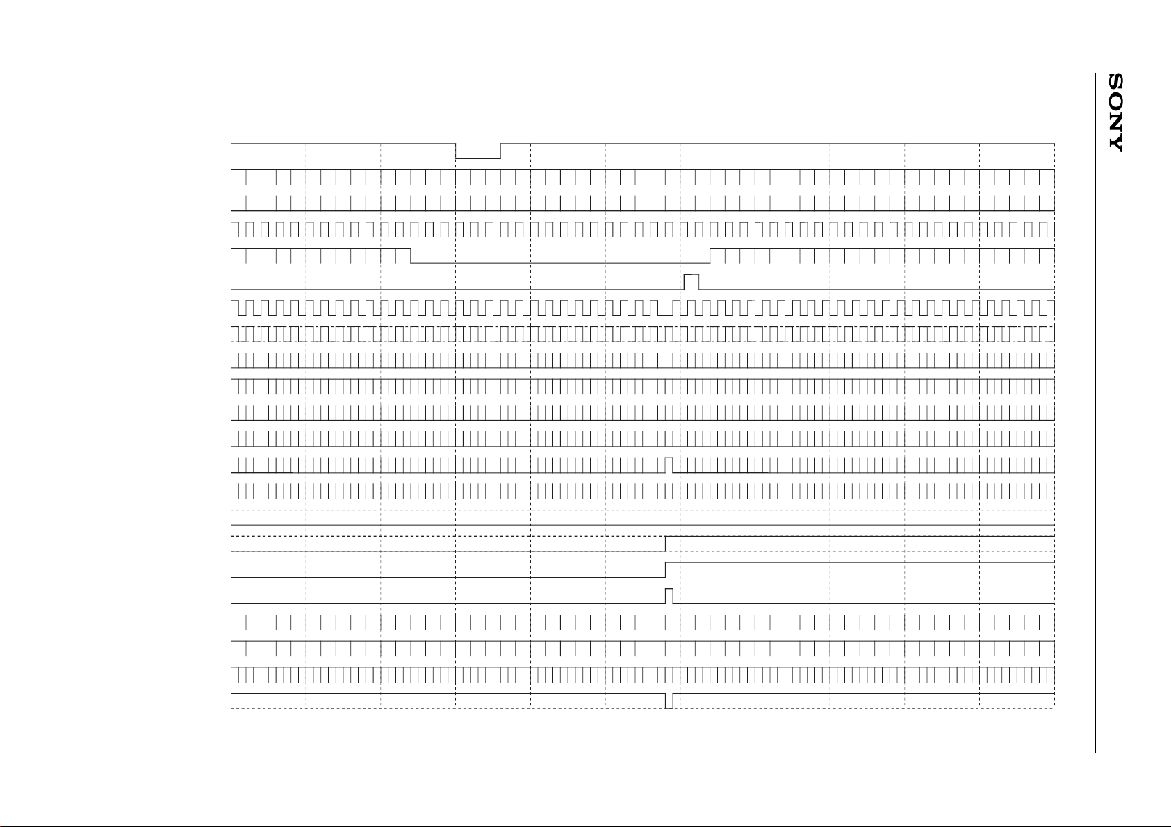
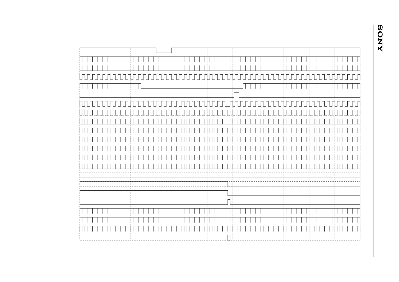
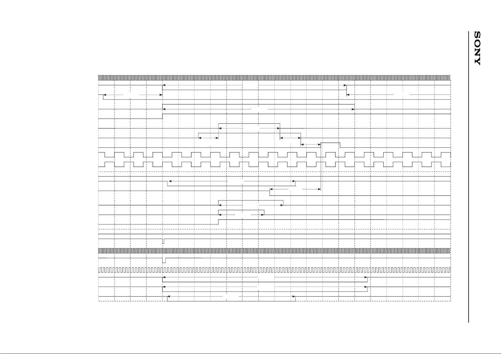
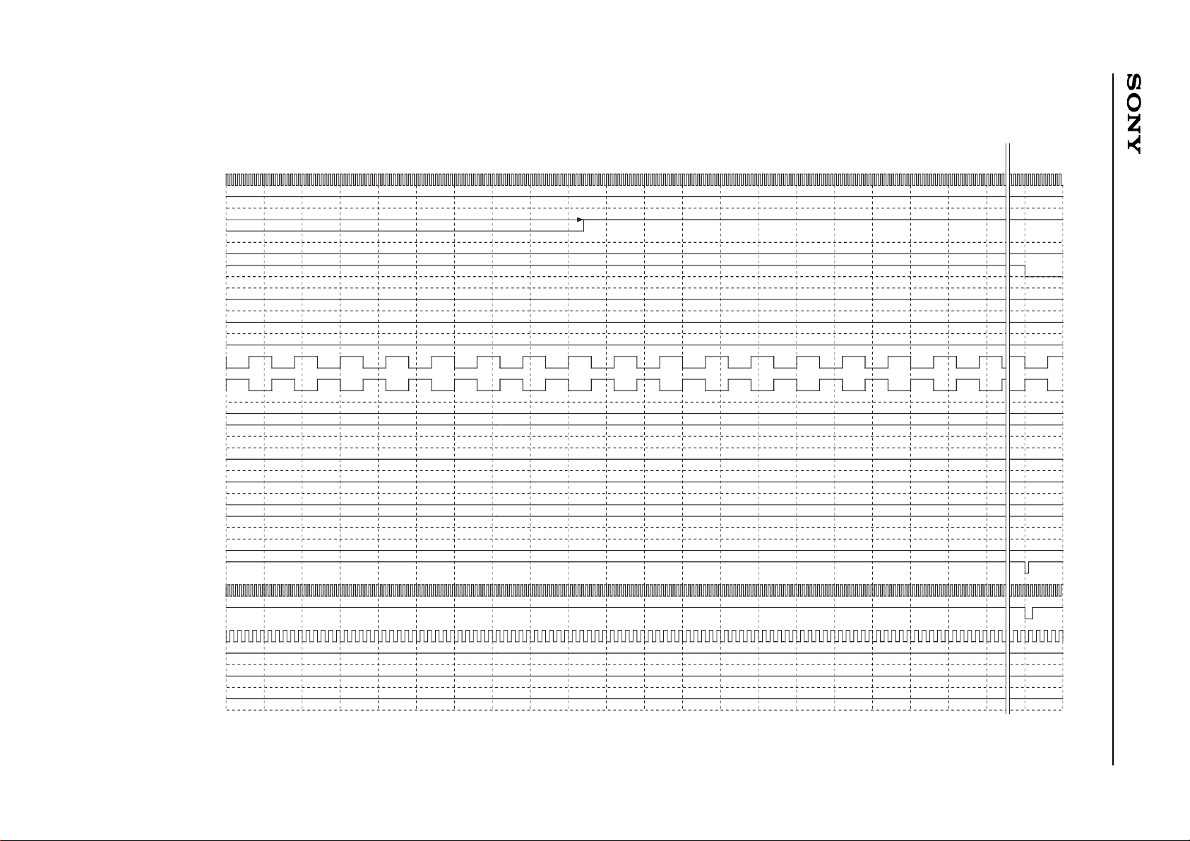
HST
ENB
CLP1
CLP2
PCG
PRG
CLR
FRP
FLDO
BLK
IRACT
ORACT
XHS
XVS
20101600
588 31
Note) When DWN is Low, VST is inversed.
The 1H and 1V cycle FRP and FLDO polarity are not specified.
The fifth row of the timing chart (BLK) is a pulse indicated as a reference and is not a pulse output from pins.
LCX026 SVGA 800 × 600
Page 42

– 42 –
CXD2464R
RGT : H PLLP : HLLLLLLHHHL (LSB) HP : HHHLHLLL (LSB) HSTP : LLHH (LSB) PCGP : LHHHL (LSB) PRGP : HLHLL (LSB)
CLPP : LL (LSB) HPOL : L HDNPOL : H CLPPOL : H PCGPOL : H PRGPOL : H HR : H HST : H PCG : H DSP : H
Loop Counter : 1040 clk
MCK f : 50.00MHz (20.00ns)
MCK
HSYNC
(BLK)
HD
HDN
CLP1
CLP2
HST
HCK1
HCK2
CLR
VCK
PCG
FRP
BLK
RSTR
RCK
WCK
ORACT
XHS
ENB
PRG
RSTW
IRACT
910 920 930 940 950 960 970 980 990 1000 1010 1020 1030 0 10 20 30 40 50 60 70 80 89
56 clk
120 clk
120 clk
19 clk
32 clk
128 clk
128 clk
34 clk
Note) When RGT is Low, HCK1 and 2 are inversed.
The third row of the timing chart (BLK) is a pulse indicated as a reference and is not a pulse output from pins.
LCX026 SVGA_1 800 × 600
Page 43

– 43 –
CXD2464R
RGT : H PLLP : HLLLLLLHHHL (LSB) HP : HHHLHLLL (LSB) HSTP : LLHH (LSB) PCGP : LHHHL (LSB) PRGP : HLHLL (LSB)
CLPP : LL (LSB) HPOL : L HDNPOL : H CLPPOL : H PCGPOL : H PRGPOL : H HR : H HST : H PCG : H DSP : H
Loop Counter : 1040 clk
MCK f : 50.00MHz (20.00ns)
MCK
HSYNC
(BLK)
HD
HDN
CLP1
CLP2
HST
HCK1
HCK2
CLR
ENB
VCK
PRG
PCG
FRP
BLK
RSTR
RCK
RSTW
WCK
IRACT
ORACT
XHS
90 100 110 120 130 140 160 170 180 190 200 210 220 230 240 250 260 270 280 290 300 309
64 clk
19 clk
19 clk
150
58 clk
48 clk
120 clk
84 clk
60 clk
Note) When RGT is Low, HCK1 and 2 are inversed.
The third row of the timing chart (BLK) is a pulse indicated as a reference and is not a pulse output from pins.
LCX026 SVGA_2 800 × 600
Page 44

– 44 –
CXD2464R
MODE3/2/1 : H/H/L MODE B/A : H/H MODE021 : L DWN : H VP : LLLHLHLL (LSB) MBK2/1/0/B/A : H/H/H/L/L FRP1/0 : H/H VPOL : L VGAV : H PC98 : H
VSYNC
HSYNC
HD
HDN
(BLK)
VST
VCK
FRP
HST
ENB
CLP1
CLP2
PCG
PRG
CLR
FRP
FLDO
BLK
IRACT
ORACT
XHS
XVS
470 480 1 10 20 30 40 49
1 2
460
Note) When DWN is Low, VST is inversed.
The 1H and 1V cycle FRP and FLDO polarity are not specified.
The fifth row of the timing chart (BLK) is a pulse indicated as a reference and is not a pulse output from pins.
LCX026 VGA 640 × 480
Page 45

– 45 –
CXD2464R
RGT : H PLLP : LHHLLHHHHHL (LSB) HP : HHLLHLHL (LSB) HSTP : LLHH (LSB) PCGP : LHLLH (LSB) PRGP : LHHLH (LSB)
CLPP : LL (LSB) HPOL : L HDNPOL : H CLPPOL : H PCGPOL : H PRGPOL : H HR : H HST : H PCG : H DSP : H
Loop Counter : 832 clk
MCK f : 31.50MHz (31.75ns)
MCK
HSYNC
(BLK)
HD
HDN
CLP1
CLP2
HST
HCK1
HCK2
CLR
ENB
VCK
PRG
PCG
FRP
BLK
RSTR
RCK
RSTW
WCK
IRACT
ORACT
XHS
792 802 812 822 0 10 20 30 40 50 60 70 80 90 100 110 120 130 140 150 160 170 180
24 clk
40 clk
120 clk
128 clk
38 clk
13 clk
32 clk
80 clk
56 clk
40 clk
128 clk
128 clk
32 clk
34 clk
13 clk
13 clk
Note) When RGT is Low, HCK1 and 2 are inversed.
The third row of the timing chart (BLK) is a pulse indicated as a reference and is not a pulse output from pins.
LCX026 VGA 640 × 480
Page 46
– 46 –
CXD2464R
MODE3/2/1 : H/H/L MODE B/A : H/H MODE021 : L DWN : H VP : LLLLHHLL (LSB) MBK2/1/0/B/A : H/H/H/L/L FRP1/0 : H/H VPOL : L VGAV : L PC98 : H
VSYNC
HSYNC
HD
HDN
(BLK)
VST
VCK
FRP
HST
ENB
CLP1
CLP2
PCG
PRG
CLR
FRP
FLDO
BLK
IRACT
ORACT
XHS
XVS
474 480 485 2320101
1 2
Note) When DWN is Low, VST is inversed.
The 1H and 1V cycle FRP polarity is not specified.
The fifth row of the timing chart (BLK) is a pulse indicated as a reference and is not a pulse output from pins.
LCX026 NTSC (ODD) 640 × 480
Page 47
– 47 –
CXD2464R
MODE3/2/1 : H/H/L MODE B/A : H/H MODE021 : L DWN : H VP : LLLLHHLL (LSB) MBK2/1/0/B/A : H/H/H/L/L FRP1/0 : H/H VPOL : L VGAV : L PC98 : H
VSYNC
HSYNC
HD
HDN
(BLK)
VST
VCK
FRP
HST
ENB
CLP1
CLP2
PCG
PRG
CLR
FRP
FLDO
BLK
IRACT
ORACT
XHS
XVS
231 240 243 266260250244
1 2
Note) When DWN is Low, VST is inversed.
The 1H and 1V cycle FRP polarity is not specified.
The fifth row of the timing chart (BLK) is a pulse indicated as a reference and is not a pulse output from pins.
LCX026 NTSC (EVEN) 640 × 480
Page 48
– 48 –
CXD2464R
Loop Counter : 1560 clk
MCK f : 24.54MHz (40.75ns)
RGT : H PLLP : HHLLLLHLHHL (LSB) HP : HHHHHHLL (LSB) HSTP : LLHH (LSB) PCGP : LLHHL (LSB) PRGP : LHLLH (LSB)
CLPP : LL (LSB) HPOL : L HDNPOL : H CLPPOL : H PCGPOL : H PRGPOL : H HR : H HST : H PCG : H DSP : L
MCK
HSYNC
(BLK)
HD
HDN
CLP1
CLP2
HST
HCK1
HCK2
CLR
ENB
VCK
PRG
PCG
FRP
BLK
RSTR
RCK
RSTW
WCK
IRACT
ORACT
XHS
1520 1530 1540 1550 0 10 20 30 40 50 60 70 80 90 100 110 120 130 140 150 160 170 179
37 clk
115 clk
115 clk
38 clk
13 clk
32 clk
80 clk
40 clk
28 clk
128 clk
128 clk
80 clk
120 clk
13 clk
13 clk
Note) When RGT is Low, HCK1 and 2 are inversed.
The third row of the timing chart (BLK) is a pulse indicated as a reference and is not a pulse output from pins.
LCX026 NTSC_1 640 × 480
Page 49
– 49 –
CXD2464R
Loop Counter : 1560 clk
MCK f : 24.54MHz (40.75ns)
RGT : H PLLP : HHLLLLHLHHL (LSB) HP : HHHHHHLL (LSB) HSTP : LLLH (LSB) PCGP : LLHHL (LSB) PRGP : LHLLH (LSB)
CLPP : LL (LSB) HPOL : L HDNPOL : H CLPPOL : H PCGPOL : H PRGPOL : H HR : H HST : H PCG : H DSP : L
180 190 200 210 220 230 240 250 260 270 280 290 300 310 320 330 340 350 360 370 380 780 789
MCK
HSYNC
(BLK)
HD
HDN
CLP1
CLP2
HST
HCK1
HCK2
CLR
ENB
VCK
PRG
PCG
FRP
BLK
RSTR
RCK
RSTW
WCK
IRACT
ORACT
XHS
Note) When RGT is Low, HCK1 and 2 are inversed.
The third row of the timing chart (BLK) is a pulse indicated as a reference and is not a pulse output from pins.
LCX026 NTSC_2 640 × 480
Page 50
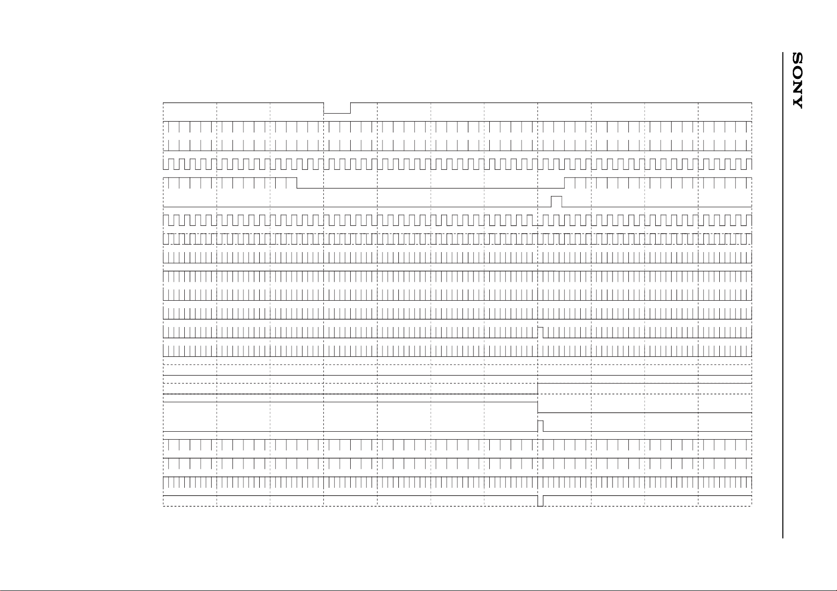
– 50 –
CXD2464R
MODE3/2/1 : L/H/L MODE B/A : H/H MODE021 : L DWN : H VP : LLLHLLHL (LSB) MBK2/1/0/B/A : H/H/H/L/L FRP1/0 : H/H VPOL : L VGAV : L PC98 : H
VSYNC
HSYNC
HD
HDN
(BLK)
VST
VCK
FRP
HST
ENB
CLP1
CLP2
PCG
PRG
CLR
FRP
FLDO
BLK
IRACT
ORACT
XHS
XVS
276 280 288 289 300 306
1 2
Note) When DWN is Low, VST is inversed.
The 1H and 1V cycle FRP polarity is not specified.
The fifth row of the timing chart (BLK) is a pulse indicated as a reference and is not a pulse output from pins.
LCX026 PAL (ODD) 762 × 572
Page 51
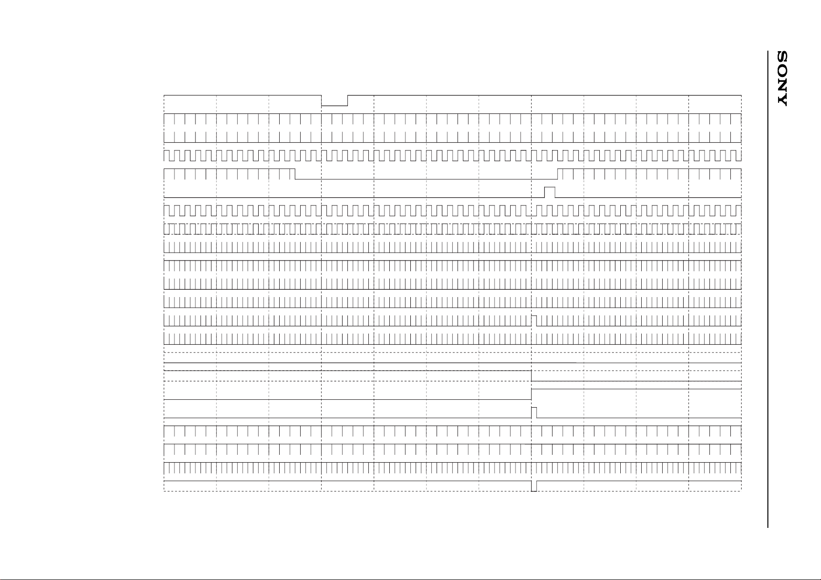
– 51 –
CXD2464R
MODE3/2/1 : L/H/L MODE B/A : H/H MODE021 : L DWN : H VP : LLLHLLHL (LSB) MBK2/1/0/B/A : H/H/H/L/L FRP1/0 : H/H VPOL : L VGAV : L PC98 : H
VSYNC
HSYNC
HD
HDN
(BLK)
VST
VCK
FRP
HST
ENB
CLP1
CLP2
PCG
PRG
CLR
FRP
FLDO
BLK
IRACT
ORACT
XHS
XVS
564 570 576 1 10
12
Note) When DWN is Low, VST is inversed.
The 1H and 1V cycle FRP polarity is not specified.
The fifth row of the timing chart (BLK) is a pulse indicated as a reference and is not a pulse output from pins.
18
LCX026 PAL (EVEN) 762 × 572
Page 52

– 52 –
CXD2464R
Loop Counter : 1880 clk
MCK f : 29.38MHz (34.04ns)
RGT : H PLLP : HHHLHLHLHHL (LSB) HP : HHLHLHLL (LSB) HSTP : LLHH (LSB) PCGP : LHLLL (LSB) PRGP : LHLHH (LSB)
CLPP : LL (LSB) HPOL : L HDNPOL : H CLPPOL : H PCGPOL : H PRGPOL : H HR : H HST : H PCG : H DSP : L
1830 1840 1850 1860 1870 0 10 20 30 40 50 60 70 80 90 100 110 120 130 140 150 160 169
MCK
HSYNC
(BLK)
HD
HDN
CLP1
CLP2
HST
HCK1
HCK2
CLR
ENB
VCK
PRG
PCG
FRP
BLK
RSTR
RCK
RSTW
WCK
IRACT
ORACT
XHS
37 clk
138 clk
120 clk
38 clk
170 clk
13 clk
32 clk
80 clk
48 clk
36 clk
128 clk
128 clk
80 clk
13 clk
13 clk
Note) When RGT is Low, HCK1 and 2 are inversed.
The third row of the timing chart (BLK) is a pulse indicated as a reference and is not a pulse output from pins.
LCX026 PAL_1 762 × 572
Page 53

– 53 –
CXD2464R
RGT : H PLLP : HHHLHLHLHHL (LSB) HP : HHLHLHLL (LSB) HSTP : LLLH (LSB) PCGP : LHLLL (LSB) PRGP : LHLHH (LSB)
CLPP : LL (LSB) HPOL : L HDNPOL : H CLPPOL : H PCGPOL : H PRGPOL : H HR : H HST : H PCG : H DSP : L
Loop Counter : 1880 clk
MCK f : 29.38MHz (34.04ns)
MCK
HSYNC
(BLK)
HD
HDN
CLP1
CLP2
HST
HCK1
HCK2
CLR
ENB
VCK
PRG
PCG
FRP
BLK
RSTR
RCK
RSTW
WCK
IRACT
ORACT
XHS
170 180 190 200 210 220 230 240 250 260 270 280 290 300 310 320 330 340 350 360 370 949
Note) When RGT is Low, HCK1 and 2 are inversed.
The third row of the timing chart (BLK) is a pulse indicated as a reference and is not a pulse output from pins.
940
LCX026 PAL_2 762 × 572
Page 54
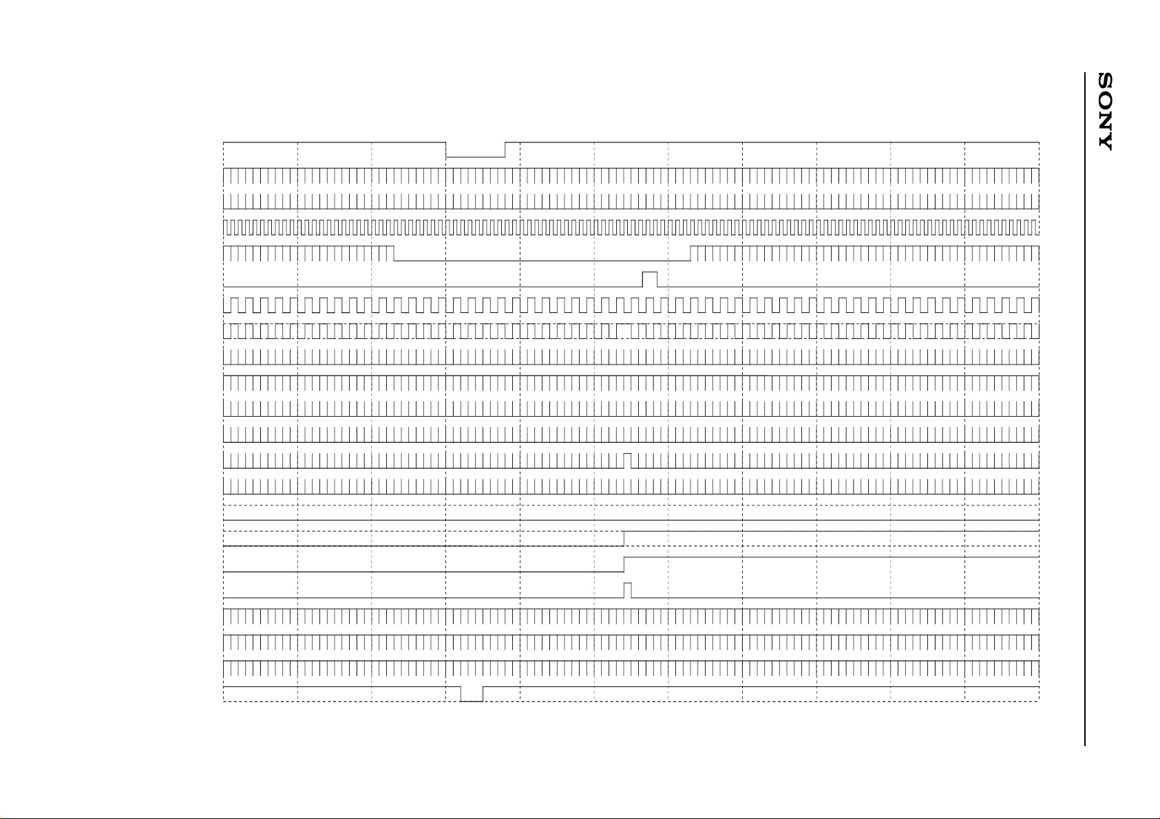
– 54 –
CXD2464R
MODE3/2/1 : L/L/H MODE B/A : H/H MODE021 : L DWN : H VP : LLLHLHHL (LSB) MBK2/1/0/B/A : H/H/H/L/L FRP1/0 : H/H VPOL : L VGAV : H PC98 : H
VSYNC
HSYNC
HD
HDN
(BLK)
VST
VCK
FRP
HST
ENB
CLP1
CLP2
PCG
PRG
CLR
FRP
FLDO
BLK
IRACT
ORACT
XHS
XVS
380 390 400 1 10 20 30 40
47
1 2
Note) When DWN is Low, VST is inversed.
The 1H and 1V cycle FRP and FLDO polarity are not specified.
The fifth row of the timing chart (BLK) is a pulse indicated as a reference and is not a pulse output from pins.
LCX026 PC98 640 × 400
Page 55

– 55 –
CXD2464R
RGT : H PLLP : LHHLHLLHHHL (LSB) HP : HHLHHHLH (LSB) HSTP : LLHH (LSB) PCGP : LLHLH (LSB) PRGP : LHLLH (LSB)
CLPP : LL (LSB) HPOL : L HDNPOL : H CLPPOL : H PCGPOL : H PRGPOL : H HR : H HST : H PCG : H DSP : H
Loop Counter : 848 clk
MCK f : 21.05MHz (47.50ns)
MCK
788 798 808 818 828 838 0 10 20 30 40 50 60 70 80 90 100 110 120 130 140 150 159
HSYNC
(BLK)
HD
HDN
CLP1
CLP2
HST
HCK1
HCK2
CLR
ENB
VCK
PRG
PCG
FRP
BLK
RSTR
RCK
RSTW
WCK
IRACT
ORACT
XHS
59 clk
64 clk
13 clk
120 clk
38 clk
80 clk
13 clk
32 clk
24 clk
36 clk
128fH
128fH
32 clk
34 clk
85 clk
13 clk
Note) When RGT is Low, HCK1 and 2 are inversed.
The third row of the timing chart (BLK) is a pulse indicated as a reference and is not a pulse output from pins.
LCX026 PC98 640 × 400
Page 56
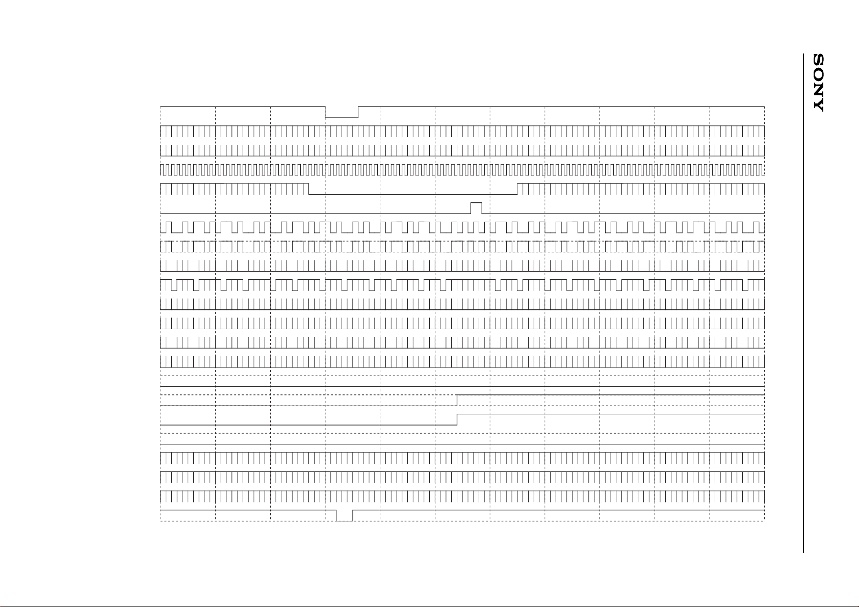
– 56 –
CXD2464R
MODE3/2/1 : L/L/L MODE B/A : H/H MODE021 : L DWN : H VP : LLLHLHHL (LSB) MBK2/1/0/B/A : H/L/H/L/L FRP1/0 : H/H VPOL : L VGAV : H PC98 : H
1 2
VSYNC
HSYNC
HD
HDN
(BLK)
VST
VCK
FRP
HST
ENB
CLP1
CLP2
PCG
PRG
CLR
FRP
FLDO
BLK
IRACT
ORACT
XHS
XVS
742 750 760 768 1 10 20 30 40 45
Note) When DWN is Low, VST is inversed.
The 1H and 1V cycle FRP and FLDO polarity are not specified.
The fifth row of the timing chart (BLK) is a pulse indicated as a reference and is not a pulse output from pins.
LCX026 XGA 1024 × 768
Page 57
– 57 –
CXD2464R
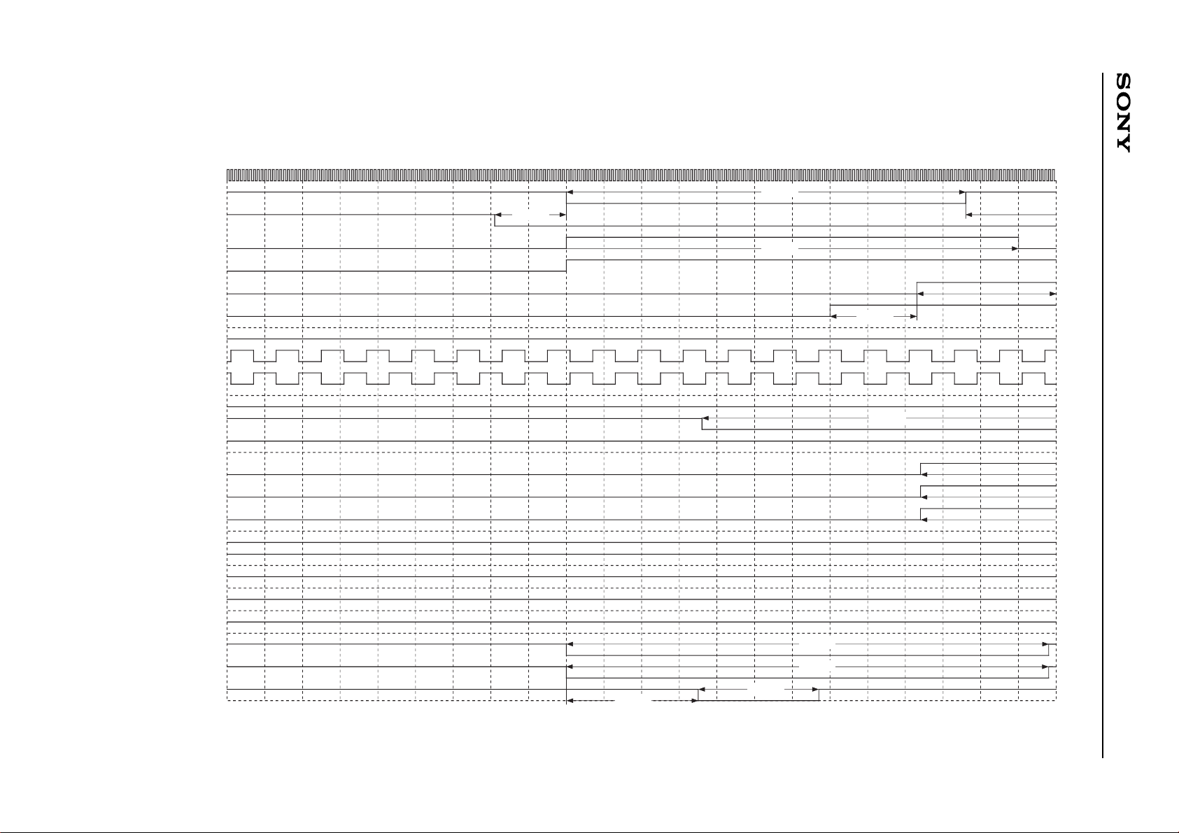
RGT : H PLLP : HLLLLLHHLLL (LSB) HP : HHLHHLHH (LSB) HSTP : HLLH (LSB) PCGP : LHHHH (LSB) PRGP : HLHLH (LSB)
CLPP : LL (LSB) HPOL : L HDNPOL : H CLPPOL : H PCGPOL : H PRGPOL : H HR : H HST : H PCG : H DSP : H
Loop Counter : 1050 clk
MCK f : 52.81MHz (18.94ns)
MCK
HSYNC
(BLK)
HD
HDN
CLP1
CLP2
HST
HCK1
HCK2
CLR
ENB
VCK
PRG
PCG
FRP
BLK
RSTR
RCK
RSTW
WCK
IRACT
ORACT
XHS
960 970 980 990 1000 1010 1020 1030 1040 0 10 20 30 40 50 60 70 80 90 100 110 120 129
19 clk
106 clk
120 clk
23 clk
143 clk
128 clk
128 clk
32 clk
34 clk
Note) When RGT is Low, HCK1 and 2 are inversed.
The third row of the timing chart (BLK) is a pulse indicated as a reference and is not a pulse output from pins.
LCX026 XGA_1 1024 × 768
Page 58

– 58 –
CXD2464R
RGT : H PLLP : HLLLLLHHLLL (LSB) HP : HHLHHLHH (LSB) HSTP : HLLH (LSB) PCGP : LHHHH (LSB) PRGP : HLHLH (LSB)
CLPP : LL (LSB) HPOL : L HDNPOL : H CLPPOL : H PCGPOL : H PRGPOL : H HR : H HST : H PCG : H DSP : H
Loop Counter : 1050 clk
MCK f : 52.81MHz (18.94ns)
130
MCK
HSYNC
(BLK)
HD
HDN
CLP1
CLP2
HST
HCK1
HCK2
CLR
ENB
VCK
PRG
PCG
FRP
BLK
RSTR
RCK
RSTW
WCK
IRACT
ORACT
XHS
140 150 160 170 180 190 200 210 220 230 240 250 260 270 280 290 300 310 320 330 340 349
125 clk
69 clk
23 clk
23 clk
143 clk
57 clk
88 clk
64 clk
Note) When RGT is Low, HCK1 and 2 are inversed.
The third row of the timing chart (BLK) is a pulse indicated as a reference and is not a pulse output from pins.
LCX026 XGA_2 1024 × 768
Page 59

– 59 –
CXD2464R
MODE3/2/1 : L/L/L MODE B/A : L/H MODE021 : L DWN : H VP : LLHLLLHH (LSB) MBK2/1/0/B/A : H/H/H/L/L FRP1/0 : H/H VPOL : L VGAV : H PC98 : H
VSYNC
HSYNC
HD
HDN
(BLK)
VST
VCK
FRP
HST
ENB
CLP1
CLP2
PCG
PRG
CLR
FRP
FLDO
BLK
IRACT
ORACT
XHS
XVS
596 600 610 620 624 1 10 20 30 38
1 2
Note) When DWN is Low, VST is inversed.
The 1H and 1V cycle FRP and FLDO polarity are not specified.
The fifth row of the timing chart (BLK) is a pulse indicated as a reference and is not a pulse output from pins.
LCX016 Macintosh16_1 832 × 624
Page 60

– 60 –
CXD2464R
RGT : H PLLP : HLLLHHHHHHL (LSB) HP : LHHLLHHH (LSB) HSTP : LLLH (LSB) PCGP : HLLLL (LSB) PRGP : HLHHH (LSB)
CLPP : LL (LSB) HPOL : L HDNPOL : H CLPPOL : H PCGPOL : H PRGPOL : H HR : H HST : H PCG : H DSP : H
Loop Counter : 1152 clk
MCK f : 57.28MHz (17.46ns)
MCK
1022
HSYNC
(BLK)
HD
HDN
CLP1
CLP2
HST
HCK1
HCK2
CLR
ENB
VCK
PRG
PCG
FRP
BLK
RSTR
RCK
RSTW
WCK
IRACT
ORACT
XHS
1032 1042 1052 1062 1072 1082 1092 1102 1112 1122 1132 1142 0 10 20 30 40 50 60 70 80 89
120 clk
32 clk
128 clk
128 clk
32 clk
34 clk
64 clk
Note) When RGT is Low, HCK1 and 2 are inversed.
The third row of the timing chart (BLK) is a pulse indicated as a reference and is not a pulse output from pins.
LCX016 Macintosh16_1 832 × 624
Page 61
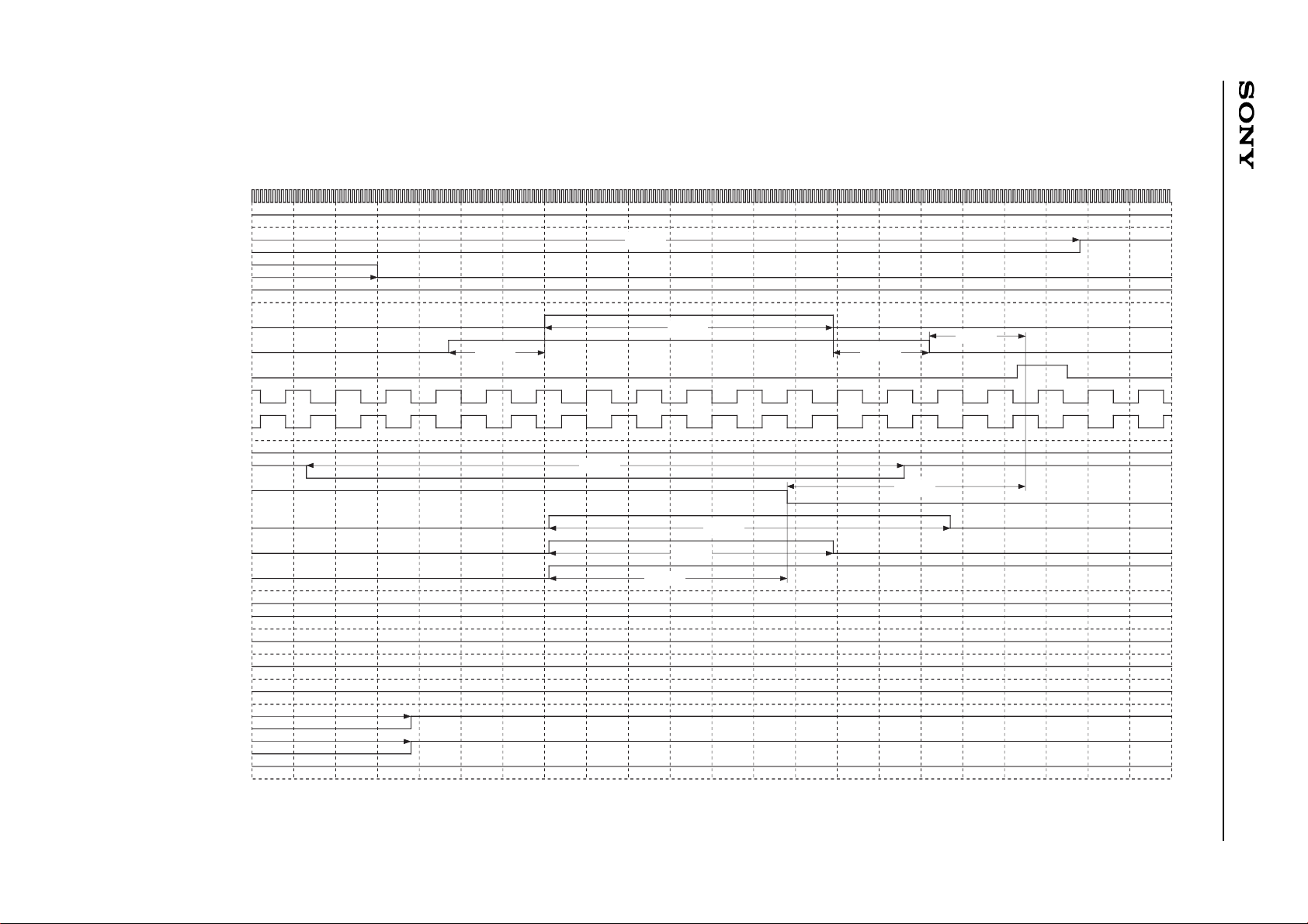
– 61 –
CXD2464R
Loop Counter : 1152 clk
MCK f : 57.28MHz (17.46ns)
RGT : H PLLP : HLLLHHHHHHL (LSB) HP : LHHLLHHH (LSB) HSTP : LLLH (LSB) PCGP : HLLLL (LSB) PRGP : HLHHH (LSB)
CLPP : LL (LSB) HPOL : L HDNPOL : H CLPPOL : H PCGPOL : H PRGPOL : H HR : H HST : H PCG : H DSP : H
MCK
90
HSYNC
(BLK)
HD
HDN
CLP1
CLP2
HST
HCK1
HCK2
CLR
ENB
VCK
PRG
PCG
FRP
BLK
RSTR
RCK
RSTW
WCK
IRACT
ORACT
XHS
100 110 120 130 140 150 160 170 180 190 200 210 220 230 240 250 260 270 280 290 300 309
224 clk
57 clk
69 clk
143 clk
96 clk
57 clk
68 clk
23 clk
23 clk
23 clk
Note) When RGT is Low, HCK1 and 2 are inversed.
The third row of the timing chart (BLK) is a pulse indicated as a reference and is not a pulse output from pins.
LCX016 Macintosh16_2 832 × 624
Page 62
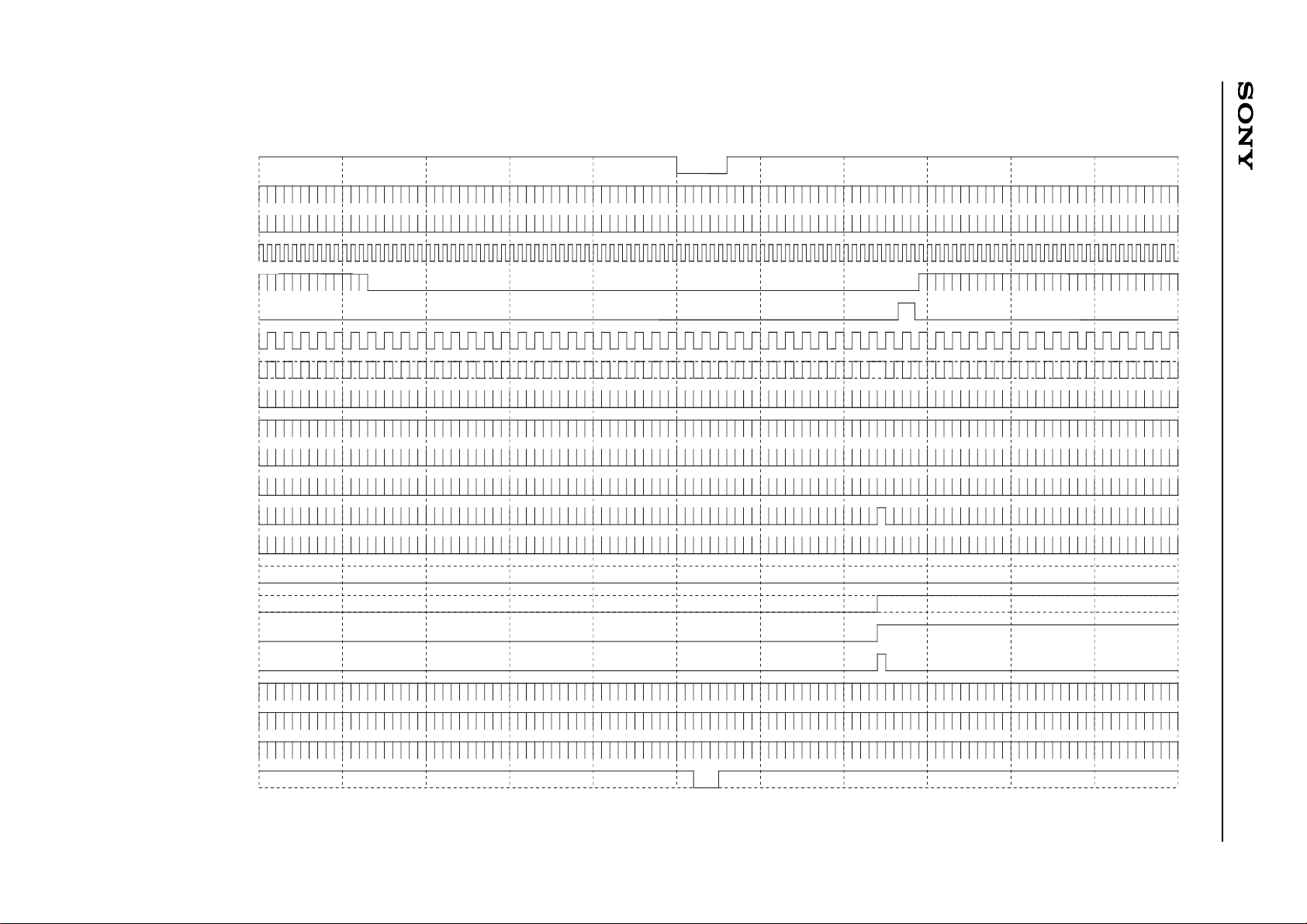
– 62 –
CXD2464R
LCX016 SVGA 800 × 600
MODE3/2/1 : H/L/L MODE B/A : L/H MODE021 : L DWN : H VP : LLHLLHHL (LSB) MBK2/1/0/B/A : H/H/H/L/L FRP1/0 : H/H VPOL : L VGAV : H PC98 : H
VSYNC
HSYNC
HD
HDN
(BLK)
VST
VCK
FRP
HST
ENB
CLP1
CLP2
PCG
PRG
CLR
FRP
FLDO
BLK
IRACT
ORACT
XHS
XVS
588 600 1 10 20 31
1 2
Note) When DWN is Low, VST is inversed.
The 1H and 1V cycle FRP and FLDO polarity are not specified.
The fifth row of the timing chart (BLK) is a pulse indicated as a reference and is not a pulse output from pins.
Page 63

– 63 –
CXD2464R
LCX016 SVGA_1 800 × 600
RGT : H PLLP : HLLLHHHHHHL (LSB) HP : HHHLLLHL (LSB) HSTP : LLLH (LSB) PCGP : LHHHL (LSB) PRGP : HLHLL (LSB)
CLPP : LL (LSB) HPOL : L HDNPOL : H CLPPOL : H PCGPOL : H PRGPOL : H HR : H HST : H PCG : H DSP : H
Loop Counter : 1040 clk
MCK f : 50.00MHz (20.00ns)
910
MCK
HSYNC
(BLK)
HD
HDN
CLP1
CLP2
HST
HCK1
HCK2
CLR
ENB
VCK
PRG
PCG
FRP
BLK
RSTR
RCK
RSTW
WCK
IRACT
ORACT
XHS
920 930 940 950 960 970 980 990 1000 1010 1020 1030 0 10 20 30 40 50 60 70 80 89
19 clk
120 clk
120 clk
56 clk
32 clk
34 clk
128 clk
128 clk
Note) When RGT is Low, HCK1 and 2 are inversed.
The third row of the timing chart (BLK) is a pulse indicated as a reference and is not a pulse output from pins.
Page 64

– 64 –
CXD2464R
RGT : H PLLP : HLLLHHHHHHL (LSB) HP : HHHLLLHL (LSB) HSTP : LLLH (LSB) PCGP : LHHHL (LSB) PRGP : HLHLL (LSB)
CLPP : LL (LSB) HPOL : L HDNPOL : H CLPPOL : H PCGPOL : H PRGPOL : H HR : H HST : H PCG : H DSP : H
Loop Counter : 1040 clk
MCK f : 50.00MHz (20.00ns)
MCK
90 100 110 120 130 140 150 160 170 180 190 200 210 220 230 240 250 260 270 280 290 300 309
HSYNC
(BLK)
HD
HDN
CLP1
CLP2
HST
HCK1
HCK2
CLR
ENB
VCK
PRG
PCG
FRP
BLK
RSTR
RCK
RSTW
WCK
IRACT
ORACT
XHS
64 clk
19 clk
19 clk
58 clk
120 clk
48 clk
84fH
60fH
Note) When RGT is Low, HCK1 and 2 are inversed.
The third row of the timing chart (BLK) is a pulse indicated as a reference and is not a pulse output from pins.
LCX016 SVGA_2 800 × 600
Page 65

– 65 –
CXD2464R
MODE3/2/1 : H/H/L MODE B/A : L/H MODE021 : L DWN : H VP : LLLHHLLL (LSB) MBK2/1/0/B/A : H/H/H/L/L FRP1/0 : H/H VPOL : L VGAV : H PC98 : H
12
VSYNC
HSYNC
HD
HDN
(BLK)
VST
VCK
FRP
HST
ENB
CLP1
CLP2
PCG
PRG
CLR
FRP
FLDO
BLK
IRACT
XHS
XVS
460 470 1 10 20 30 40 49480
ORACT
Note) When DWN is Low, VST is inversed.
The 1H and 1V cycle FRP and FLDO polarity are not specified.
The fifith row of the timing chart (BLK) is a pulse indicated as a reference and is not a pulse output from pins.
LCX016 VGA 640 × 480
Page 66
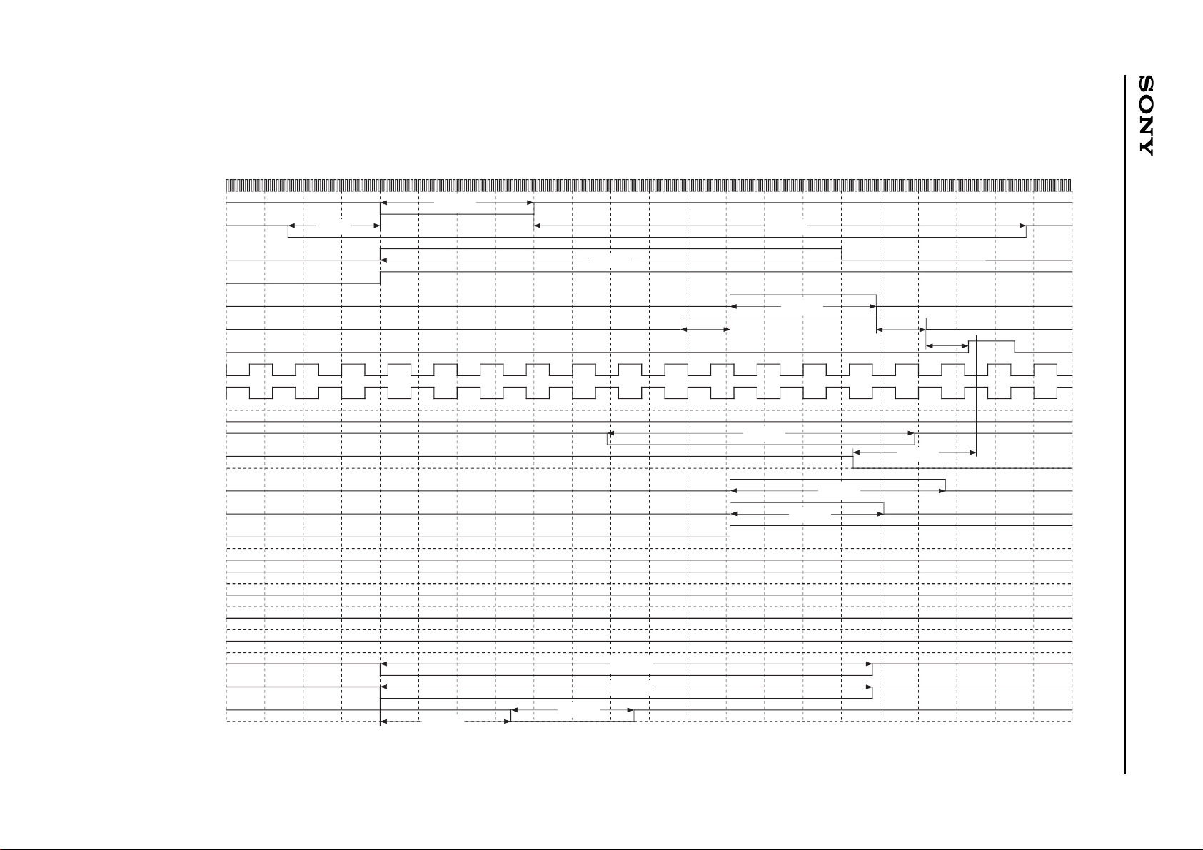
– 66 –
CXD2464R
RGT : H PLLP : LHHLLHHHHHL (LSB) HP : HHLLLHLL (LSB) HSTP : LLLH (LSB) PCGP : LHLLH (LSB) PRGP : LHHLH (LSB)
CLPP : LL (LSB) HPOL : L HDNPOL : H CLPPOL : H PCGPOL : H PRGPOL : H HR : H HST : H PCG : H DSP : H
Loop Counter : 832 clk
MCK f : 31.50MHz (31.75ns)
MCK
792 802 812 822 0 10 20 30 40 50 60 70 80 90 100 110 120 130 140 150 160 170 180
HSYNC
(BLK)
HD
HDN
CLP1
CLP2
HST
HCK1
HCK2
CLR
ENB
VCK
PRG
PCG
FRP
BLK
RSTR
RCK
RSTW
WCK
IRACT
ORACT
XHS
128 clk
120 clk
40 clk
24 clk
13 clk
38 clk
13 clk
80 clk
40 clk
56 clk
32 clk
128 clk
128 clk
32 clk
34 clk
13 clk
Note) When RGT is Low, HCK1 and 2 are inversed.
The third row of the timing chart (BLK) is a pulse indicated as a reference and is not a pulse output from pins.
LCX016 VGA 640 × 480
Page 67
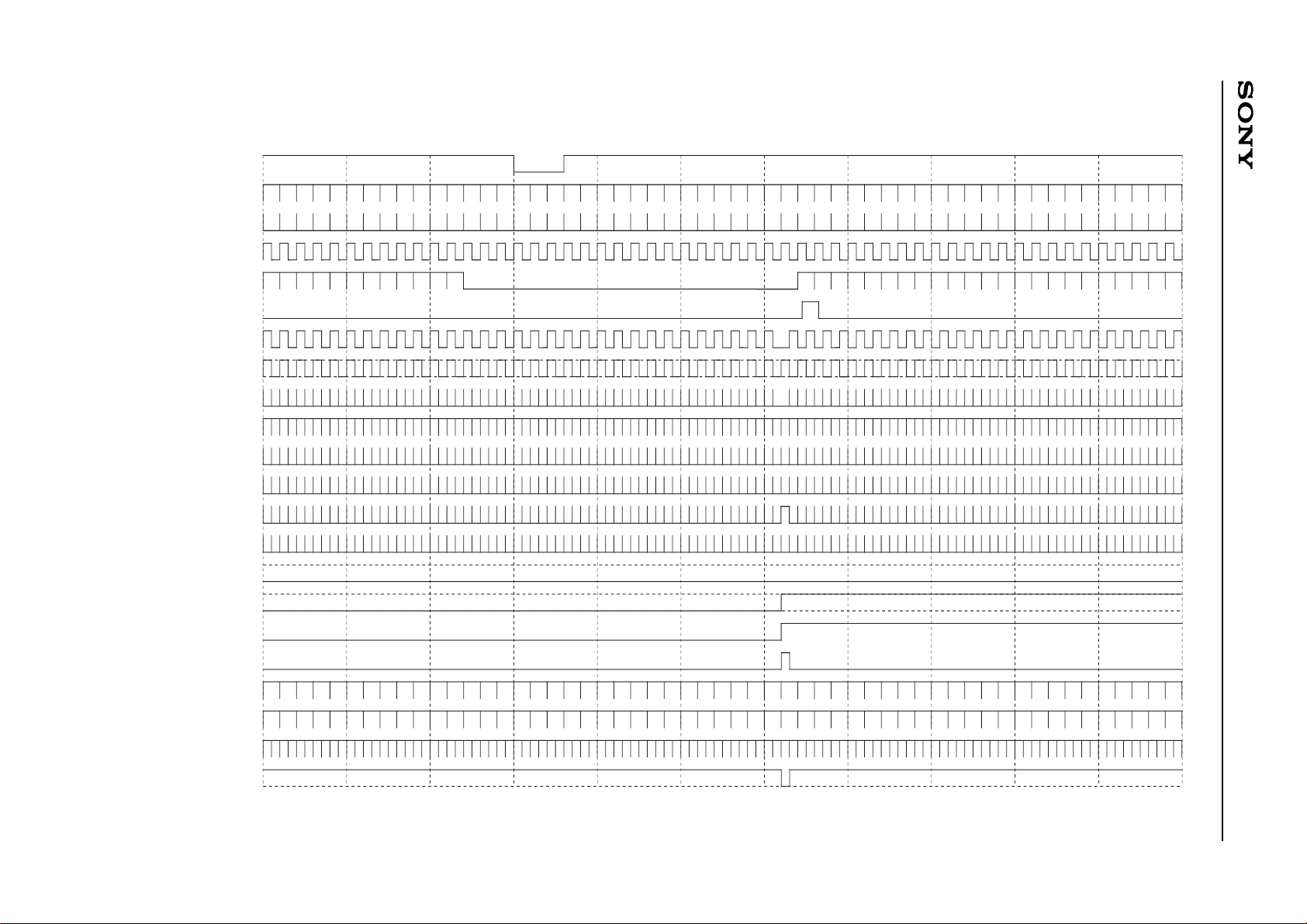
– 67 –
CXD2464R
MODE3/2/1 : H/H/L MODE B/A : L/H MODE021 : L DWN : H VP : LLLLHHHL (LSB) MBK2/1/0/B/A : H/H/H/L/L FRP1/0 : H/H VPOL : L VGAV : L PC98 : H
VSYNC
HSYNC
HD
HDN
(BLK)
VST
VCK
FRP
HST
ENB
CLP1
CLP2
PCG
PRG
CLR
FRP
FLDO
BLK
IRACT
ORACT
XHS
XVS
2320101
485480
474
12
Note) When DWN is Low, VST is inversed.
The 1H and 1V cycle FRP polarity is not specified.
The fifth row of the timing chart (BLK) is a pulse indicated as a reference and is not a pulse output from pins.
LCX016 NTSC (ODD) 640 × 480
Page 68
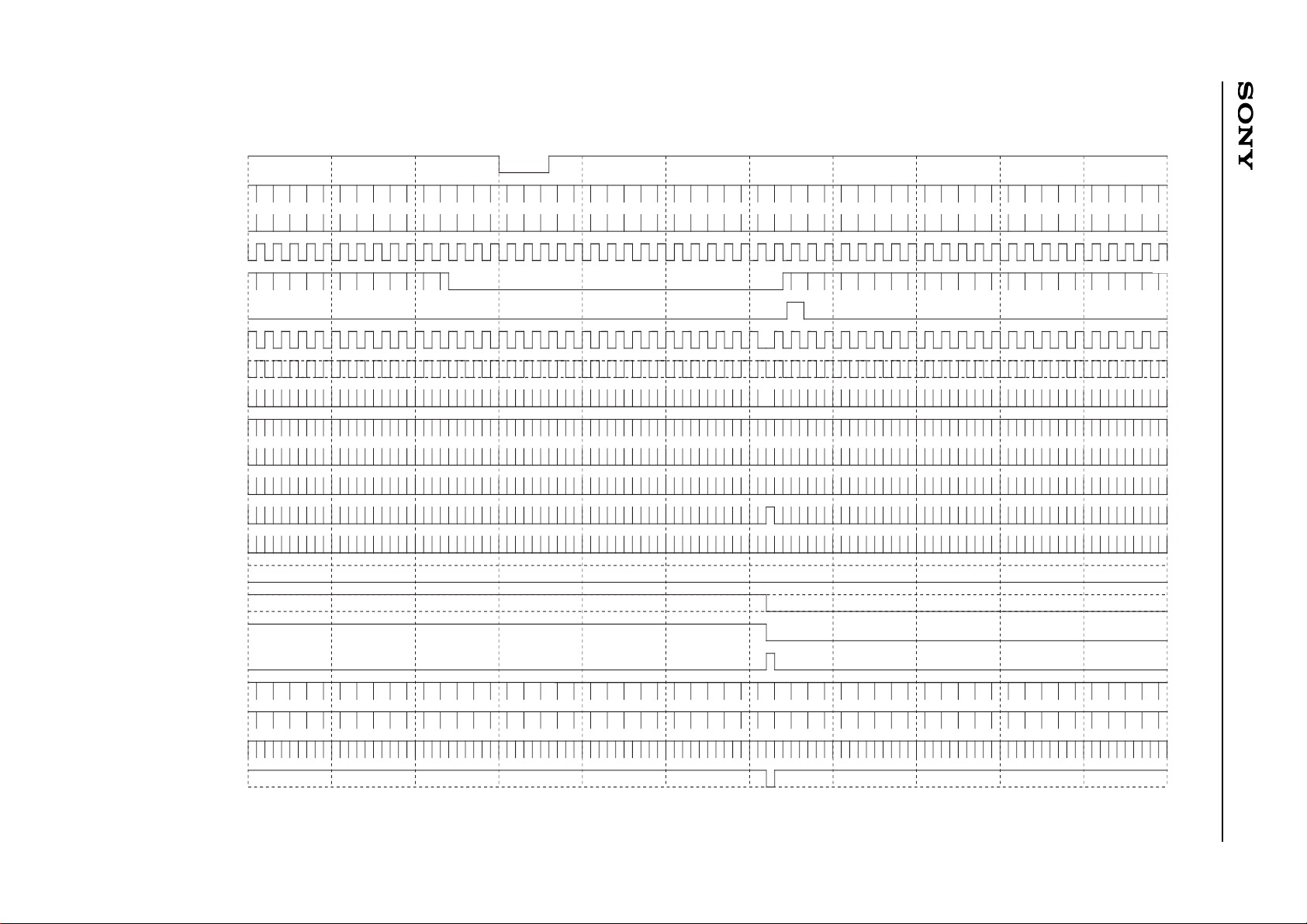
– 68 –
CXD2464R
MODE3/2/1 : H/H/L MODE B/A : L/H MODE021 : L DWN : H VP : LLLLHHHL (LSB) MBK2/1/0/B/A : H/H/H/L/L FRP1/0 : H/H VPOL : L VGAV : L PC98 : H
VSYNC
HSYNC
HD
HDN
(BLK)
VST
VCK
FRP
HST
ENB
CLP1
CLP2
PCG
PRG
CLR
FRP
FLDO
BLK
IRACT
ORACT
XHS
XVS
243
240
231
244 250 260
266
1 2
Note) When DWN is Low, VST is inversed.
The 1H and 1V cycle FRP polarity is not specified.
The fifth row of the timing chart (BLK) is a pulse indicated as a reference and is not a pulse output from pins.
LCX016 NTSC (EVEN) 640 × 480
Page 69
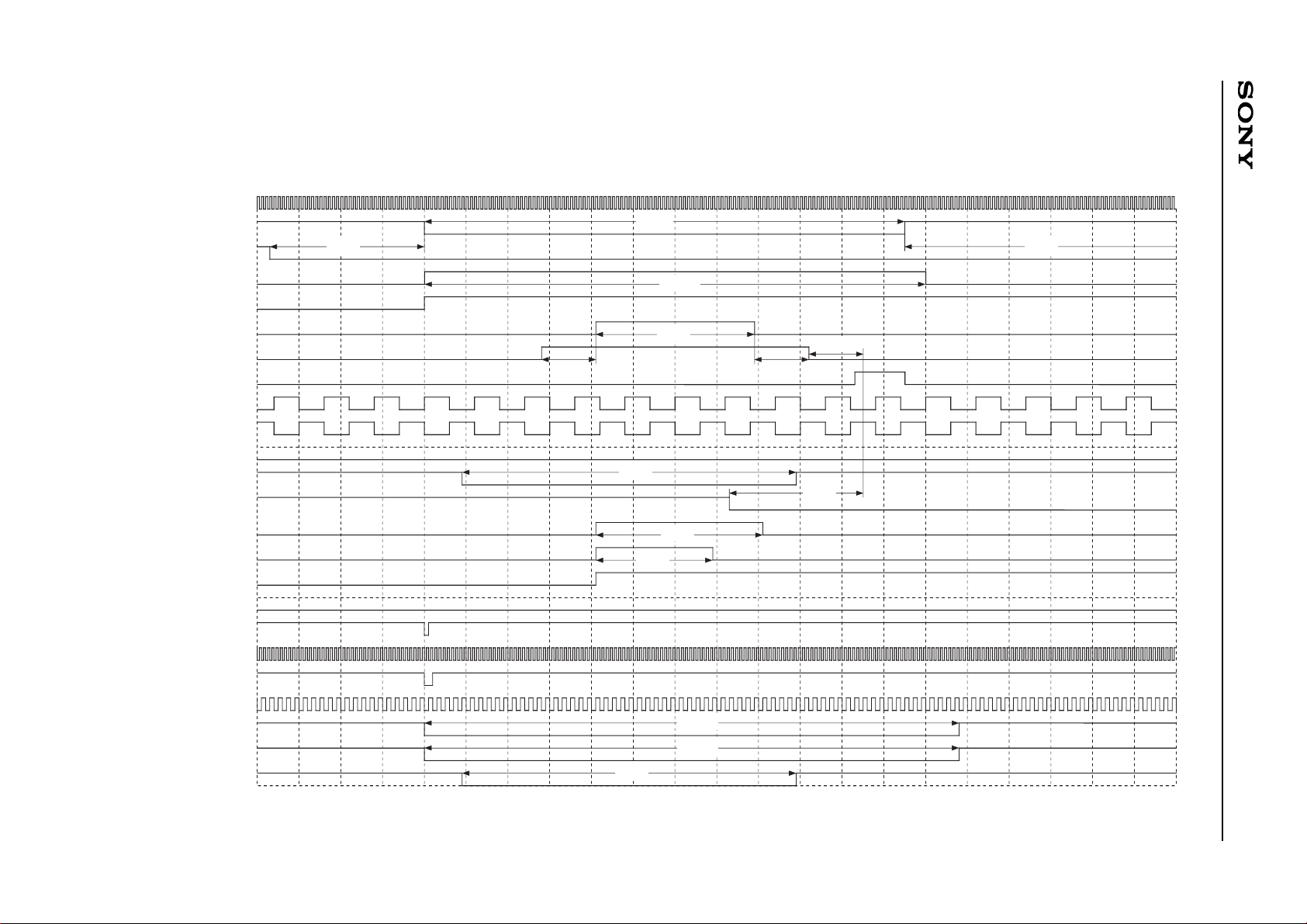
– 69 –
CXD2464R
Loop Counter : 1560 clk
MCK f : 24.54MHz (40.75ns)
RGT : H PLLP : HHLLLLHLHHL (LSB) HP : HHHHLHHL (LSB) HSTP : LLLH (LSB) PCGP : LLHHL (LSB) PRGP : LHLLH (LSB)
CLPP : LL (LSB) HPOL : L HDNPOL : H CLPPOL : H PCGPOL : H PRGPOL : H HR : H HST : H PCG : H DSP : L
1520 1530 1540 1550 0 10 20 30 40 50 60 70 80 90 100 110 120 130 140 150 160 170 179
115fH
115 clk
120 clk
38 clk
13 clk 13 clk
13 clk
32 clk
80 clk
40 clk
28 clk
80 clk
128 clk
128 clk
37 clk
MCK
HSYNC
(BLK)
HD
HDN
CLP1
CLP2
HST
HCK1
HCK2
CLR
ENB
VCK
PRG
PCG
FRP
BLK
RSTR
RCK
RSTW
WCK
IRACT
ORACT
XHS
Note) When RGT is Low, HCK1 and 2 are inversed.
The third row of the timing chart (BLK) is a pulse indicated as a reference and is not a pulse output from pins.
LCX016 NTSC_1 640 × 480
Page 70

– 70 –
CXD2464R
Loop Counter : 1560 clk
MCK f : 24.54MHz (40.75ns)
RGT : H PLLP : HHLLLLHLHHL (LSB) HP : HHHHLHHL (LSB) HSTP : LLLH (LSB) PCGP : LLHHL (LSB) PRGP : LHLLH (LSB)
CLPP : LL (LSB) HPOL : L HDNPOL : H CLPPOL : H PCGPOL : H PRGPOL : H HR : H HST : H PCG : H DSP : L
180 190 200 210 220 230 240 250 260 270 280 290 300 310 320 330 340 350 360 370 380 780 789
MCK
HSYNC
(BLK)
HD
HDN
CLP1
CLP2
HST
HCK1
HCK2
CLR
ENB
VCK
PRG
PCG
FRP
BLK
RSTR
RCK
RSTW
WCK
IRACT
ORACT
XHS
Note) When RGT is Low, HCK1 and 2 are inversed.
The third row of the timing chart (BLK) is a pulse indicated as a reference and is not a pulse output from pins.
LCX016 NTSC_2 640 × 480
Page 71
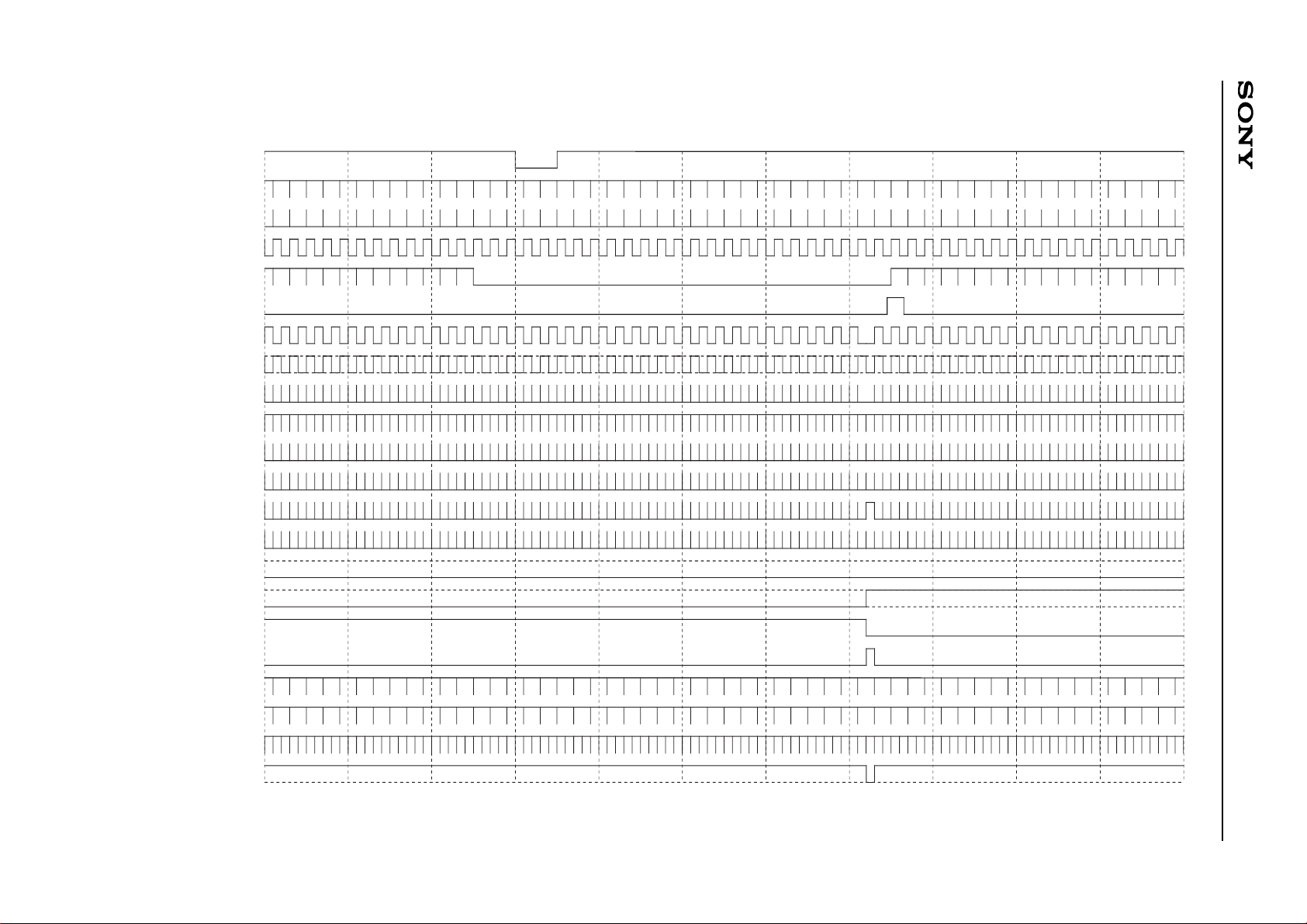
– 71 –
CXD2464R
MODE3/2/1 : L/H/L MODE B/A : L/H MODE021 : L DWN : H VP : LLLHLLHH (LSB) MBK2/1/0/B/A : H/H/H/L/L FRP1/0 : H/H VPOL : L VGAV : L PC98 : H
VSYNC
HSYNC
HD
HDN
(BLK)
VST
VCK
FRP
HST
ENB
CLP1
CLP2
PCG
PRG
CLR
FRP
FLDO
BLK
IRACT
ORACT
XHS
XVS
300
306289
1 2
288280276
Note) When DWN is Low, VST is inversed.
The 1H and 1V cycle FRP polarity is not specified.
The fifth row of the timing chart (BLK) is a pulse indicated as a reference and is not a pulse output from pins.
LCX016 PAL (ODD) 762 × 572
Page 72
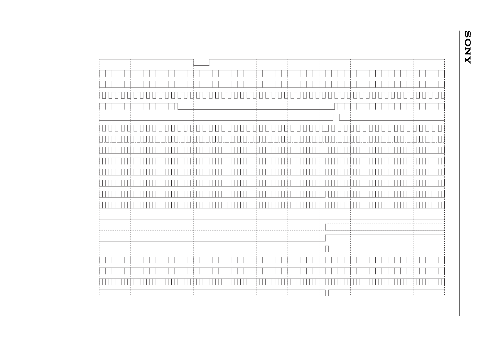
– 72 –
CXD2464R
MODE3/2/1 : L/H/L MODE B/A : L/H MODE021 : L DWN : H VP : LLLHLLHH (LSB) MBK2/1/0/B/A : H/H/H/L/L FRP1/0 : H/H VPOL : L VGAV : L PC98 : H
VSYNC
HSYNC
HD
HDN
(BLK)
VST
VCK
FRP
HST
ENB
CLP1
CLP2
PCG
PRG
CLR
FRP
FLDO
BLK
IRACT
ORACT
XHS
XVS
101 18576570
564
12
Note) When DWN is Low, VST is inversed.
The 1H and 1V cycle FRP polarity is not specified.
The fifth row of the timing chart (BLK) is a pulse indicated as a reference and is not a pulse output from pins.
LCX016 PAL (EVEN) 762 × 572
Page 73
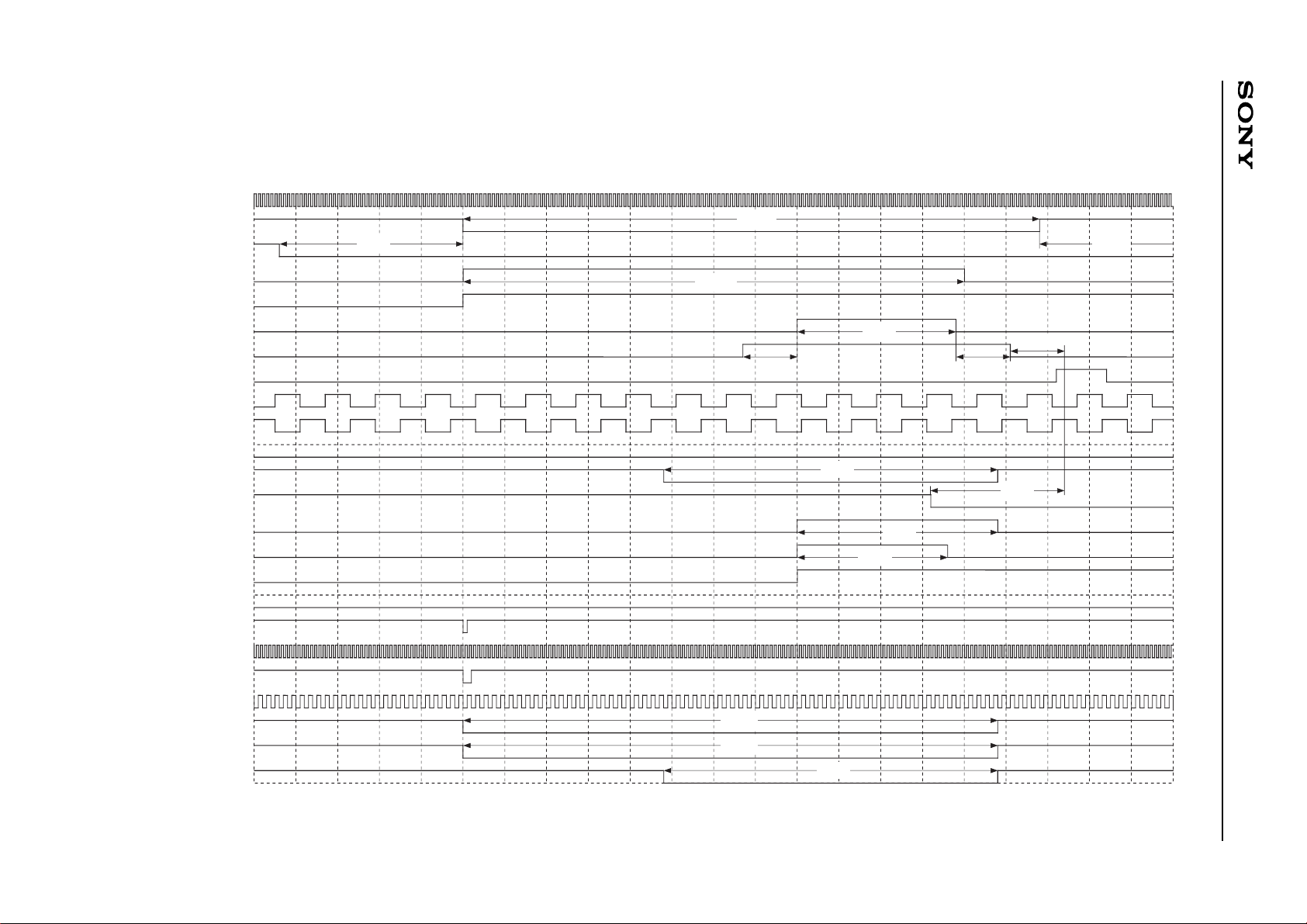
– 73 –
CXD2464R
Loop Counter : 1880 clk
MCK f : 29.38MHz (34.04ns)
RGT : H PLLP : HHHLHLHLHHL (LSB) HP : HHLLHHHH (LSB) HSTP : LLLH (LSB) PCGP : LHLLL (LSB) PRGP : LHLHH (LSB)
CLPP : LL (LSB) HPOL : L HDNPOL : H CLPPOL : H PCGPOL : H PRGPOL : H HR : H HST : H PCG : H DSP : L
1830 1840 1850 1860 1870 0 10 20 30 40 50 60 70 80 90 100 110 120 130 140 150 160 169
MCK
HSYNC
(BLK)
HD
HDN
CLP1
CLP2
HST
HCK1
HCK2
CLR
ENB
VCK
PRG
PCG
FRP
BLK
RSTR
RCK
RSTW
WCK
IRACT
ORACT
XHS
13 clk
13 clk
38 clk
13 clk
138 clk
120 clk
32 clk
37 clk
80 clk
48 clk
36 clk
80 clk
128 clk
128 clk
Note) When RGT is Low, HCK1 and 2 are inversed.
The third row of the timing chart (BLK) is a pulse indicated as a reference and is not a pulse output from pins.
170 clk
LCX016 PAL_1 762 × 572
Page 74
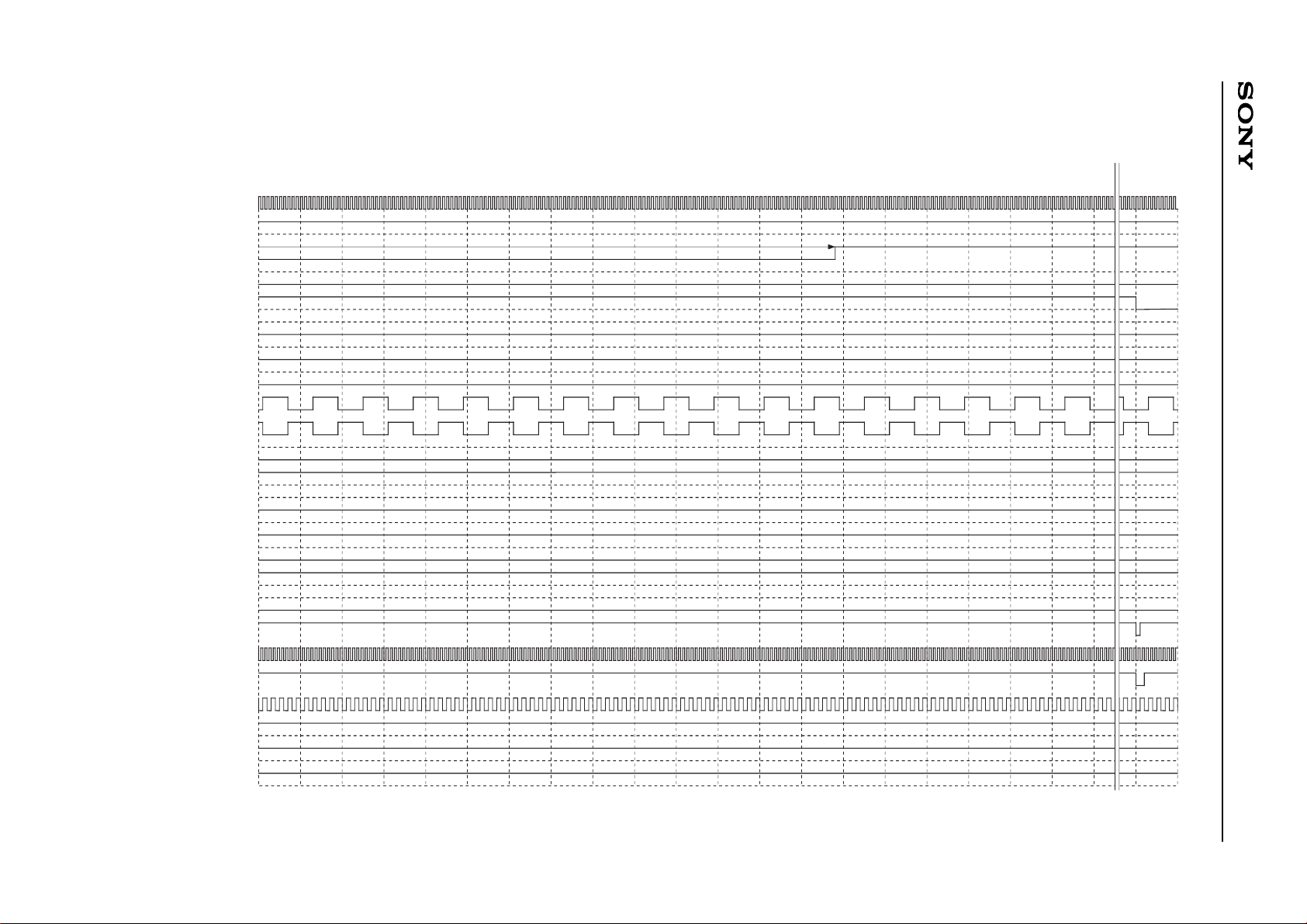
– 74 –
CXD2464R
RGT : H PLLP : HHHLHLHLHHL (LSB) HP : HHLLHHHH (LSB) HSTP : LLLH (LSB) PCGP : LHLLL (LSB) PRGP : LHLHH (LSB)
CLPP : LL (LSB) HPOL : L HDNPOL : H CLPPOL : H PCGPOL : H PRGPOL : H HR : H HST : H PCG : H DSP : L
Loop Counter : 1880 clk
MCK f : 29.38MHz (34.04ns)
170 180 190 200 210 220 230 240 250 260 270 280 290 300 310 320 330 340 350 360 370 940 949
MCK
HSYNC
(BLK)
HD
HDN
CLP1
CLP2
HST
HCK1
HCK2
CLR
ENB
VCK
PRG
PCG
FRP
BLK
RSTR
RCK
RSTW
WCK
IRACT
ORACT
XHS
Note) When RGT is Low, HCK1 and 2 are inversed.
The third row of the timing chart (BLK) is a pulse indicated as a reference and is not a pulse output from pins.
LCX016 PAL_2 762 × 572
Page 75
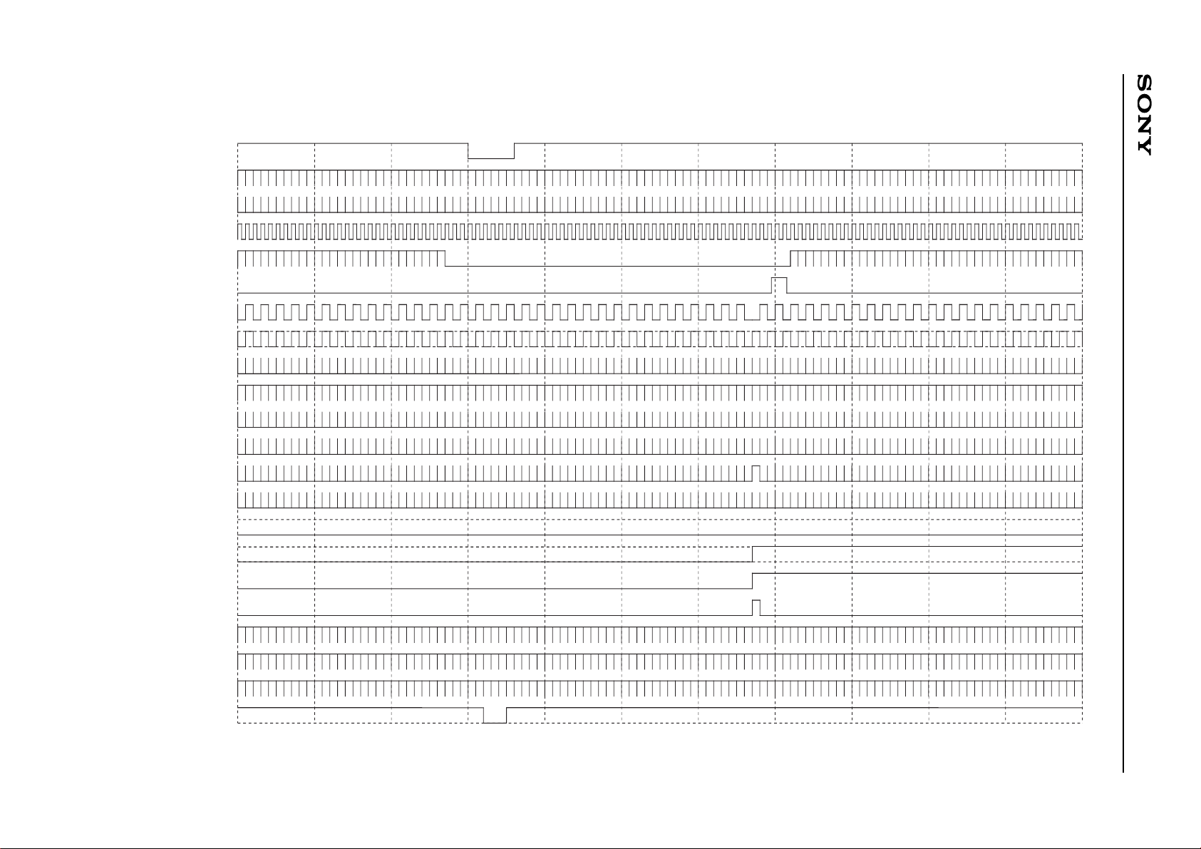
– 75 –
CXD2464R
MODE3/2/1 : H/L/H MODE B/A : L/H MODE021 : L DWN : H VP : LLLHHLLL (LSB) MBK2/1/0/B/A : H/H/H/L/L FRP1/0 : H/H VPOL : L VGAV : H PC98 : H
VSYNC
HSYNC
HD
HDN
(BLK)
VST
VCK
FRP
HST
ENB
CLP1
CLP2
PCG
PRG
CLR
FRP
FLDO
BLK
IRACT
ORACT
XHS
XVS
480 1 10 20 30470460454
1 2
Note) When DWN is Low, VST is inversed.
The 1H and 1V cycle FRP and FLDO polarity are not specified.
The fifth row of the timing chart (BLK) is a pulse indicated as a reference and is not a pulse output from pins.
49
LCX016 NTSC_WIDE 832 × 480
Page 76

– 76 –
CXD2464R
RGT : H PLLP : LHHLLHHHHHL (LSB) HP : HHLLHHHL (LSB) HSTP : LLLH (LSB) PCGP : LHLLH (LSB) PRGP : LHHLH (LSB)
CLPP : LL (LSB) HPOL : L HDNPOL : H CLPPOL : H PCGPOL : H PRGPOL : H HR : H HST : H PCG : H DSP : H
Loop Counter : 1014 clk
MCK f : 31.90MHz (31.35ns)
974 984 994 1004 0 10 20 30 40 50 60 70 80 90 100 110 120 130 140 150 160 170 180
MCK
HSYNC
(BLK)
HD
HDN
CLP1
CLP2
HST
HCK1
HCK2
CLR
ENB
VCK
PRG
PCG
FRP
BLK
RSTR
RCK
RSTW
WCK
IRACT
ORACT
XHS
120 clk
79 clk
38 clk
13 clk 13 clk
13 clk
32 clk
80 clk
56 clk
40 clk
32 clk
79 clk
24 clk
34 clk
128 clk
128 clk
Note) When RGT is Low, HCK1 and 2 are inversed.
The third row of the timing chart (BLK) is a pulse indicated as a reference and is not a pulse output from pins.
LCX016 NTSC_WIDE 832 × 480
Page 77
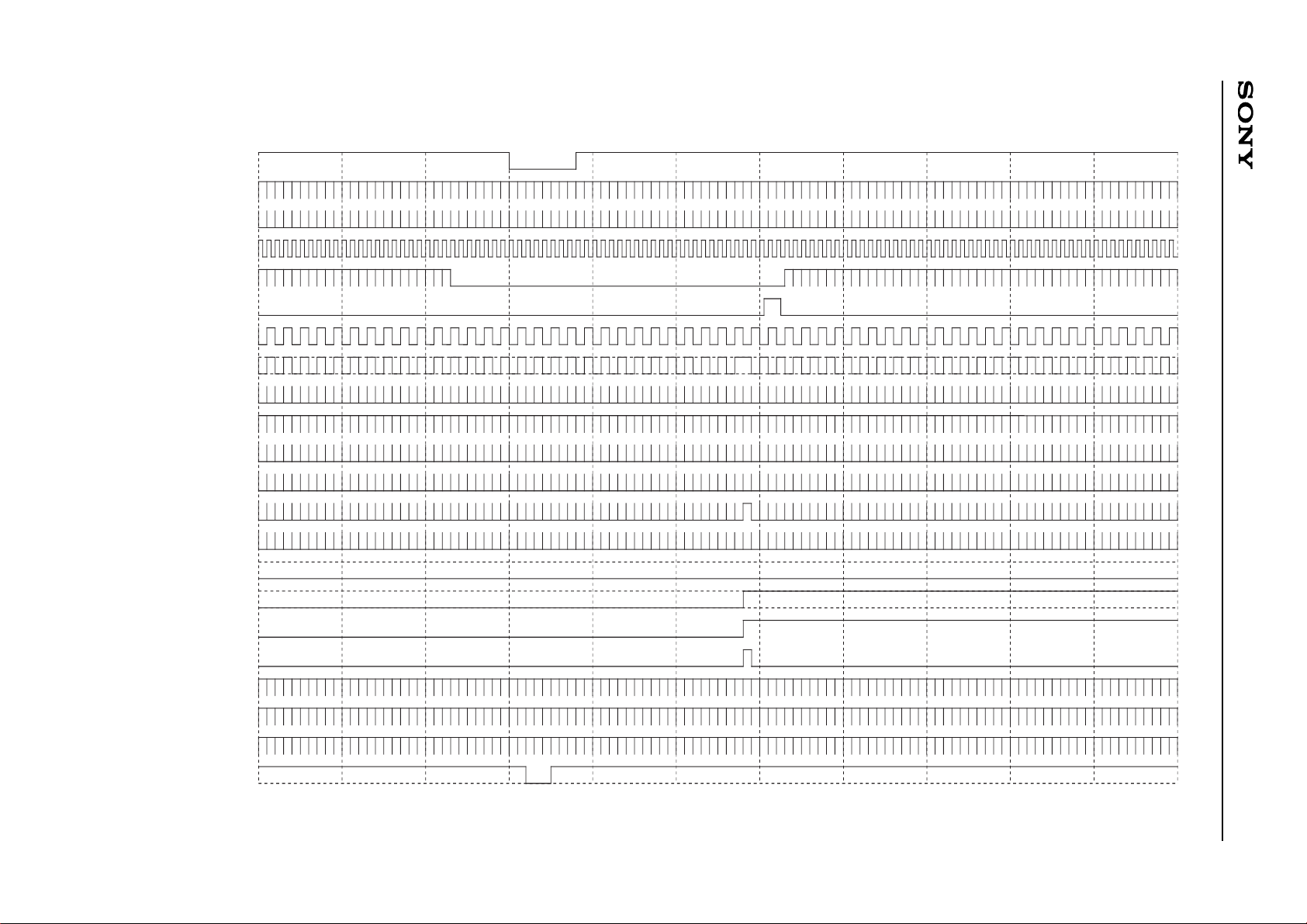
– 77 –
CXD2464R
MODE3/2/1 : L/L/H MODE B/A : L/H MODE021 : L DWN : H VP : LLLHHLHL (LSB) MBK2/1/0/B/A : H/H/H/L/L FRP1/0 : H/H VPOL : L VGAV : H PC98 : H
1400 10 20 30 40390380
VSYNC
HSYNC
HD
HDN
(BLK)
VST
VCK
FRP
HST
ENB
CLP1
CLP2
PCG
PRG
CLR
FRP
FLDO
BLK
IRACT
ORACT
XHS
XVS
12
47
Note) When DWN is Low, VST is inversed.
The 1H and 1V cycle FRP and FLDO polarity are not specified.
The fifth row of the timing chart (BLK) is a pulse indicated as a reference and is not a pulse output from pins.
LCX016 PC98 640 × 400
Page 78
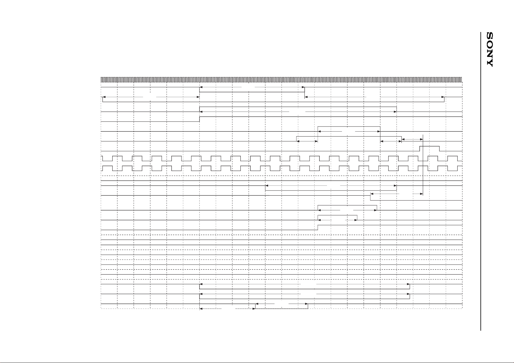
– 78 –
CXD2464R
RGT : H PLLP : LHHLHLLHHHL (LSB) HP : HHLHLHHH (LSB) HSTP : LLLH (LSB) PCGP : LLHLH (LSB) PRGP : LHLLH (LSB)
CLPP : LL (LSB) HPOL : L HDNPOL : H CLPPOL : H PCGPOL : H PRGPOL : H HR : H HST : H PCG : H DSP : H
Loop Counter : 848 clk
MCK f : 21.05MHz (47.50ns)
120 clk
38 clk
13 clk
13 clk
32 clk
80 clk
36 clk
24 clk
128 clk
128 clk
59 clk
64 clk
34 clk
788 798 808 818 828 838 0 10 20 30 40 50 60 70 80 90 100 110 120 130 140 150 159
MCK
HSYNC
(BLK)
HD
HDN
CLP1
CLP2
HST
HCK1
HCK2
CLR
ENB
VCK
PRG
PCG
FRP
BLK
RSTR
RCK
RSTW
WCK
IRACT
ORACT
XHS
13 clk
Note) When RGT is Low, HCK1 and 2 are inversed.
The third row of the timing chart (BLK) is a pulse indicated as a reference and is not a pulse output from pins.
85 clk
32 clk
LCX016 PC98 640 × 400
Page 79

– 79 –
CXD2464R
MODE3/2/1 : L/L/L MODE B/A : L/H MODE021 : L DWN : H VP : LLLHLHHL (LSB) MBK2/1/0/B/A : H/H/L/L/L FRP1/0 : H/H VPOL : L VGAV : H PC98 : H
VSYNC
HSYNC
HD
HDN
(BLK)
VST
VCK
FRP
HST
ENB
CLP1
CLP2
PCG
PRG
CLR
FRP
FLDO
BLK
IRACT
ORACT
XHS
XVS
1768 10 20 30 40
1 2
752 45
Note) When DWN is Low, VST is inversed.
The 1H and 1V cycle FRP and FLDO polarity are not specified.
The fifth row of the timing chart (BLK) is a pulse indicated as a reference and is not a pulse output from pins.
760750
LCX016 XGA 1024 × 768
Page 80

– 80 –
CXD2464R
RGT : H PLLP : HLLLHLLLLHL (LSB) HP : HHLLHLLL (LSB) HSTP : LLLH (LSB) PCGP : LHHHH (LSB) PRGP : HLHLH (LSB)
CLPP : LL (LSB) HPOL : L HDNPOL : H CLPPOL : H PCGPOL : H PRGPOL : H HR : H HST : H PCG : H DSP : H
Loop Counter : 1092 clk
MCK f : 52.81MHz (18.94ns)
1002 1012 1022 1032 1042 1052 1062 1072 1082 0 10 20 30 40 50 60 70 80 90 100 110 120 129
MCK
HSYNC
(BLK)
HD
HDN
CLP1
CLP2
HST
HCK1
HCK2
CLR
ENB
VCK
PRG
PCG
FRP
BLK
RSTR
RCK
RSTW
WCK
IRACT
ORACT
XHS
20 clk
110 clk
120 clk
128 clk
128 clk
23 clk
32 clk
34 clk
Note) When RGT is Low, HCK1 and 2 are inversed.
The third row of the timing chart (BLK) is a pulse indicated as a reference and is not a pulse output from pins.
LCX016 XGA_1 1024 × 768
Page 81

– 81 –
CXD2464R
RGT : H PLLP : HLLLHLLLLHL (LSB) HP : HHLLHLLL (LSB) HSTP : LLLH (LSB) PCGP : LHHHH (LSB) PRGP : HLHLH (LSB)
CLPP : LL (LSB) HPOL : L HDNPOL : H CLPPOL : H PCGPOL : H PRGPOL : H HR : H HST : H PCG : H DSP : H
Loop Counter : 1092 clk
MCK f : 52.81MHz (18.94ns)
69 clk
130 clk
23 clk
143 clk
57 clk
88 clk
64 clk
23 clk
130 140 150 160 170 180 190 200 210 220 230 240 250 260 270 280 290 300 310 320 330 340 349
MCK
HSYNC
(BLK)
HD
HDN
CLP1
CLP2
HST
HCK1
HCK2
CLR
ENB
VCK
PRG
PCG
FRP
BLK
RSTR
RCK
RSTW
WCK
IRACT
ORACT
XHS
Note) When RGT is Low, HCK1 and 2 are inversed.
The third row of the timing chart (BLK) is a pulse indicated as a reference and is not a pulse output from pins.
LCX016 XGA_2 1024 × 768
Page 82
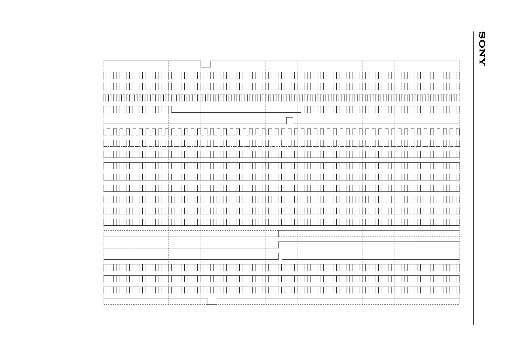
– 82 –
CXD2464R
MODE3/2/1 : H/H/L MODE B/A : L/L MODE021 : L DWN : H VP : LLLHLHHL (LSB) MBK2/1/0/B/A : H/H/H/L/L FRP1/0 : H/H VPOL : L VGAV : H PC98 : H
VSYNC
HSYNC
HD
HDN
(BLK)
VST
VCK
FRP
HST
ENB
CLP1
CLP2
PCG
PRG
CLR
FRP
FLDO
BLK
IRACT
ORACT
XHS
XVS
1
10 20 30 40 49480470460
1 2
Note) When DWN is Low, VST is inversed.
The 1H and 1V cycle FRP and FLDO polarity are not specified.
The fifth row of the timing chart (BLK) is a pulse indicated as a reference and is not a pulse output from pins.
LCX012BL VGA 640 × 480
Page 83
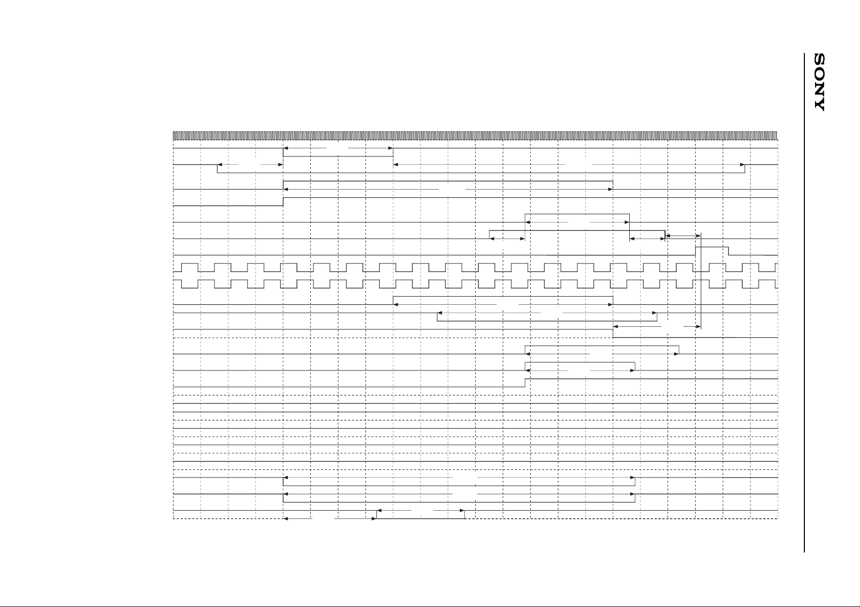
– 83 –
CXD2464R
RGT : H PLLP : LHHLLHHHHHL (LSB) HP : HHLLLHHH (LSB) HSTP : LLLH (LSB) PCGP : LHLLH (LSB) PRGP : LHHLH (LSB)
CLPP : LL (LSB) HPOL : L HDNPOL : H CLPPOL : H PCGPOL : H PRGPOL : H HR : H HST : H PCG : H DSP : H
Loop Counter : 832 clk
MCK f : 31.50MHz (31.75ns)
120 clk
38 clk
13 clk
32 clk
80 clk
56 clk
40 clk
32 clk
128 clk
128 clk
24 clk
40 clk
128 clk
34 clk
792 802 812 822 0 10 20 30 40 50 60 70 80 90 100 110 120 130 140 150 160 170 180
MCK
HSYNC
(BLK)
HD
HDN
CLP1
CLP2
HST
HCK1
HCK2
CLR
ENB
VCK
PRG
PCG
FRP
BLK
RSTR
RCK
RSTW
WCK
IRACT
ORACT
XHS
80 clk
13 clk 13 clk
Note) When RGT is Low, HCK1 and 2 have the same polarity.
The third row of the timing chart (BLK) is a pulse indicated as a reference and is not a pulse output from pins.
LCX012BL VGA 640 × 480
Page 84
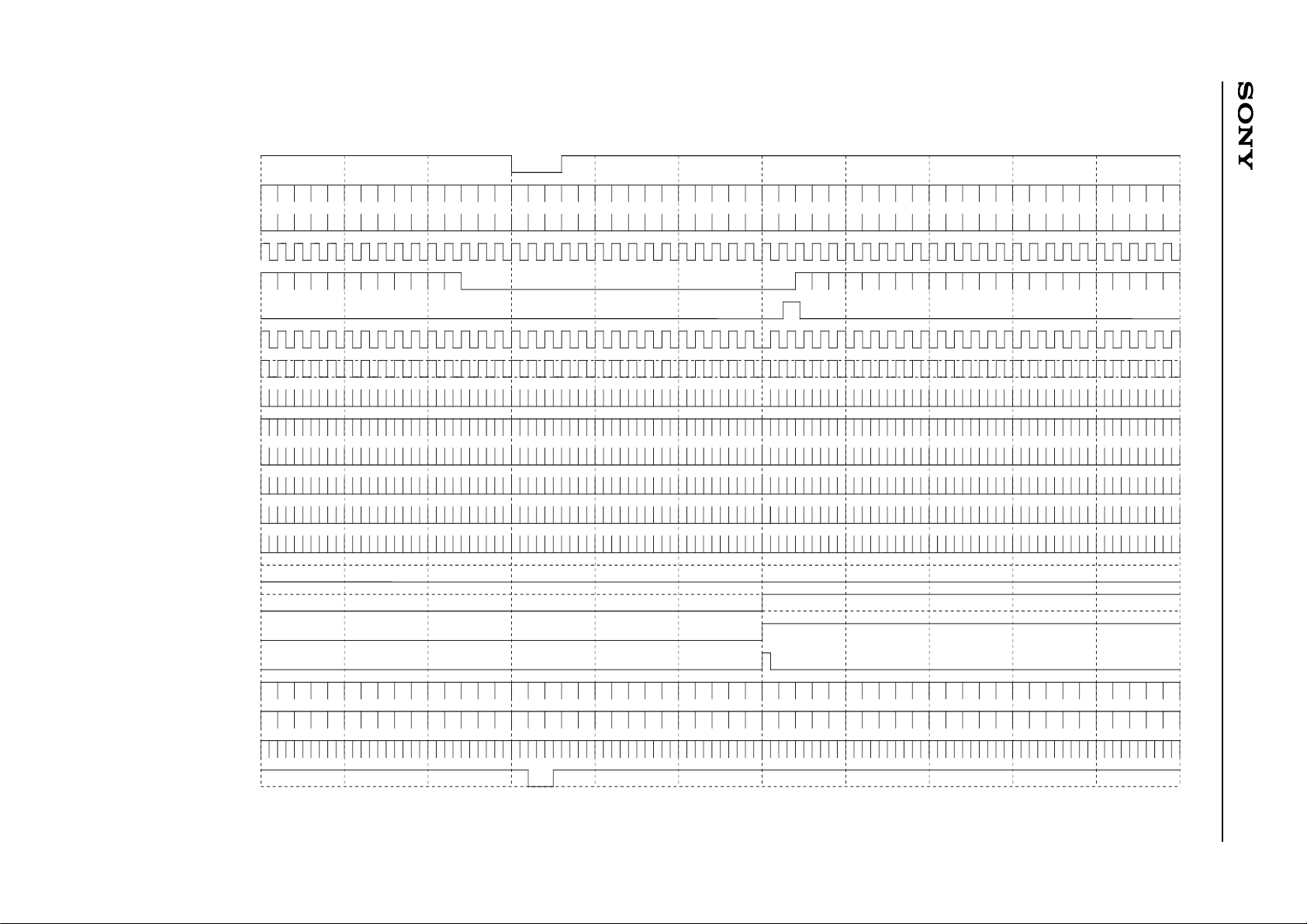
– 84 –
CXD2464R
MODE3/2/1 : H/H/L MODE B/A : L/L MODE021 : L DWN : H VP : LLLLHHLH (LSB) MBK2/1/0/B/A : H/H/H/L/L FRP1/0 : H/H VPOL : L VGAV : L PC98 : H
VSYNC
HSYNC
HD
HDN
(BLK)
VST
VCK
FRP
HST
ENB
CLP1
CLP2
PCG
PRG
CLR
FRP
FLDO
BLK
IRACT
ORACT
XHS
XVS
1485 10 20 23480
474
1 2
Note) When DWN is Low, VST is inversed.
The 1H and 1V cycle FRP polarity is not specified.
The fifth row of the timing chart (BLK) is a pulse indicated as a reference and is not a pulse output from pins.
LCX012BL NTSC (ODD) 640 × 480
Page 85
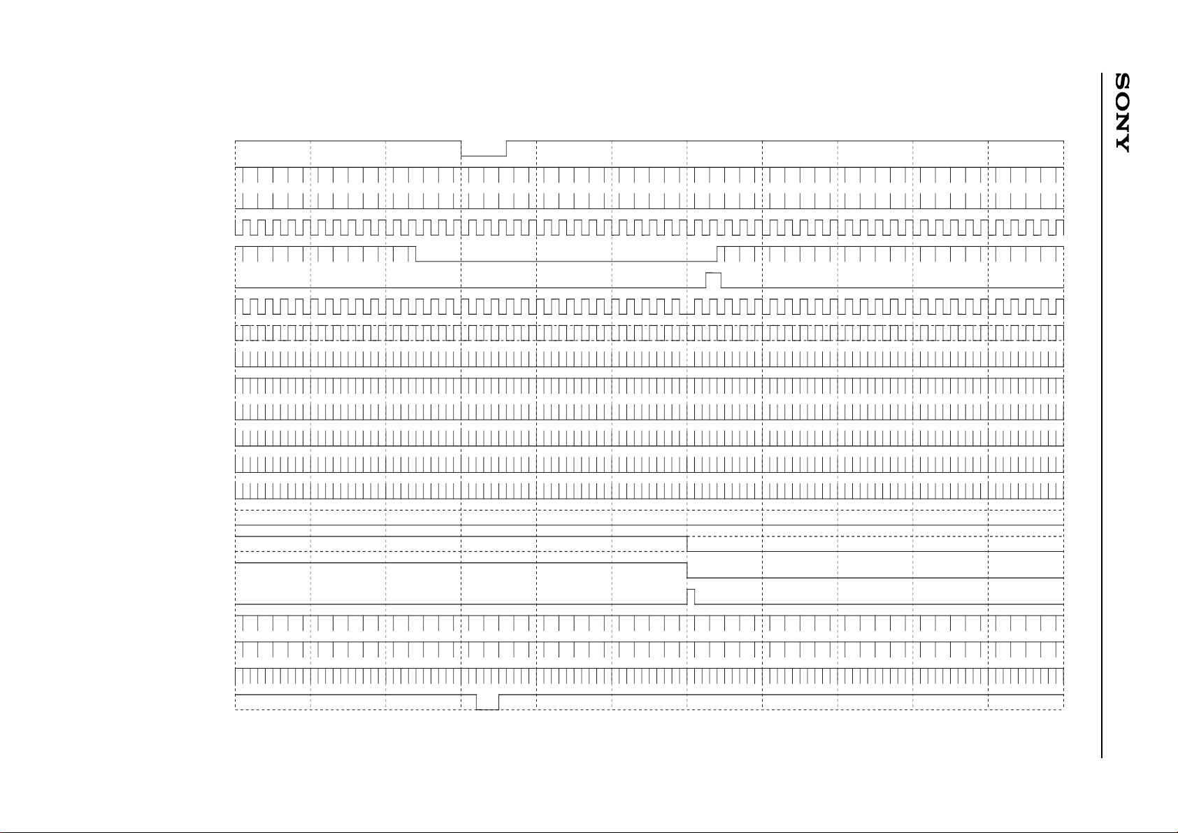
– 85 –
CXD2464R
MODE3/2/1 : H/H/L MODE B/A : L/L MODE021 : L DWN : H VP : LLLLHHLH (LSB) MBK2/1/0/B/A : H/H/H/L/L FRP1/0 : H/H VPOL : L VGAV : L PC98 : H
VSYNC
HSYNC
HD
HDN
(BLK)
VST
VCK
FRP
HST
ENB
CLP1
CLP2
PCG
PRG
CLR
FRP
FLDO
BLK
IRACT
ORACT
XHS
XVS
243240 244 250 260
266231
12
Note) When DWN is Low, VST is inversed.
The 1H and 1V cycle FRP polarity is not specified.
The fifth row of the timing chart (BLK) is a pulse indicated as a reference and is not a pulse output from pins.
LCX012BL NTSC (EVEN) 640 × 480
Page 86

– 86 –
CXD2464R
Loop Counter : 1560 clk
MCK f : 24.54MHz (40.75ns)
RGT : H PLLP : HHLLLLHLHHL (LSB) HP : HHHHHLLH (LSB) HSTP : LLLH (LSB) PCGP : LLHHL (LSB) PRGP : LHLLH (LSB)
CLPP : LL (LSB) HPOL : L HDNPOL : H CLPPOL : H PCGPOL : H PRGPOL : H HR : H HST : H PCG : H DSP : L
1520 1530 1540 1550 0 10 20 30 40 50 60 70 80 90 100 110 120 130 140 150 160 170 179
115 clk
115 clk
120 clk
38 clk
32 clk
80 clk
40 clk
28 clk
80 clk
128 clk
128 clk
37 clk
MCK
HSYNC
(BLK)
HD
HDN
CLP1
CLP2
HST
HCK1
HCK2
CLR
ENB
VCK
PRG
PCG
FRP
BLK
RSTR
RCK
RSTW
WCK
IRACT
ORACT
XHS
13 clk13 clk
Note) When RGT is Low, HCK1 and 2 have the same polarity.
The third row of the timing chart (BLK) is a pulse indicated as a reference and is not a pulse output from pins.
13 clk
LCX012BL NTSC_1 640 × 480
Page 87

– 87 –
CXD2464R
Loop Counter : 1560 clk
MCK f : 24.54MHz (40.75ns)
RGT : H PLLP : HHLLLLHLHHL (LSB) HP : HHHHHLLH (LSB) HSTP : LLLH (LSB) PCGP : LLHHL (LSB) PRGP : LHLLH (LSB)
CLPP : LL (LSB) HPOL : L HDNPOL : H CLPPOL : H PCGPOL : H PRGPOL : H HR : H HST : H PCG : H DSP : L
MCK
HSYNC
(BLK)
HD
HDN
CLP1
CLP2
HST
HCK1
HCK2
CLR
ENB
VCK
PRG
PCG
FRP
BLK
RSTR
RCK
RSTW
WCK
IRACT
ORACT
XHS
180 190 202 210 220 230 240 250 260 270 280 290 300 310 320 330 340 350 360 370 380 780 789
Note) When RGT is Low, HCK1 and 2 have the same polarity.
The third row of the timing chart (BLK) is a pulse indicated as a reference and is not a pulse output from pins.
LCX012BL NTSC_2 640 × 480
Page 88
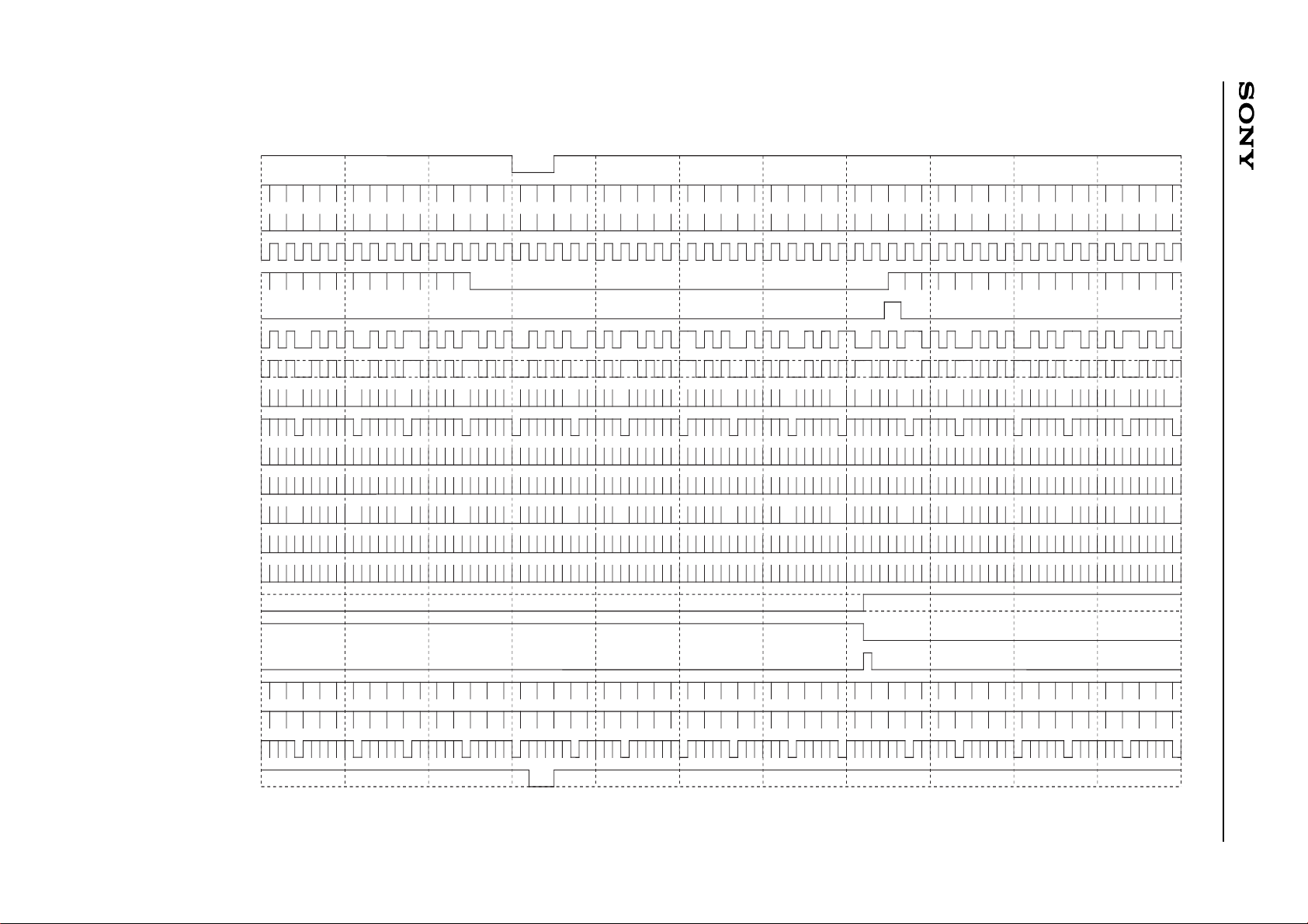
– 88 –
CXD2464R
MODE3/2/1 : H/H/L MODE B/A : L/L MODE021 : L DWN : H VP : LLLHLLHL (LSB) MBK2/1/0/B/A : H/L/L/L/L FRP1/0 : H/H VPOL : L VGAV : L PC98 : H
VSYNC
HSYNC
HD
HDN
(BLK)
VST
VCK
FRP
HST
ENB
CLP1
CLP2
PCG
PRG
CLR
FRP
FLDO
BLK
IRACT
ORACT
XHS
XVS
276 280 288 289 300 306
12
Note) When DWN is Low, VST is inversed.
The 1H and 1V cycle FRP polarity is not specified.
The fifth row of the timing chart (BLK) is a pulse indicated as a reference and is not a pulse output from pins.
LCX012BL PAL (ODD) 640 × 480
Page 89

– 89 –
CXD2464R
MODE3/2/1 : H/H/L MODE B/A : L/L MODE021 : L DWN : H VP : LLLHLLHL (LSB) MBK2/1/0/B/A : H/L/L/L/L FRP1/0 : H/H VPOL : L VGAV : L PC98 : H
VSYNC
HSYNC
HD
HDN
(BLK)
VST
VCK
FRP
HST
ENB
CLP1
CLP2
PCG
PRG
CLR
FRP
FLDO
BLK
IRACT
ORACT
XHS
XVS
564 570 576
1
10
1 2
18
Note) When DWN is Low, VST is inversed.
The 1H and 1V cycle FRP polarity is not specified.
The fifth row of the timing chart (BLK) is a pulse indicated as a reference and is not a pulse output from pins.
LCX012BL PAL (EVEN) 640 × 480
Page 90
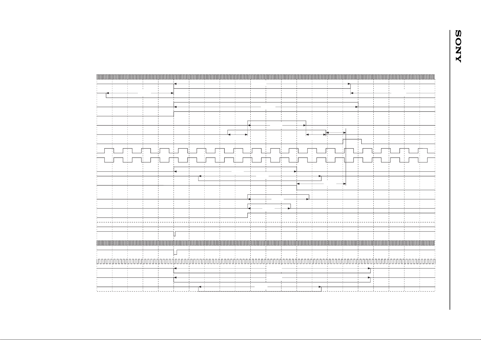
– 90 –
CXD2464R
Loop Counter : 1560 clk
MCK f : 24.38MHz (41.02ns)
RGT : H PLLP : HHLLLLHLHHL (LSB) HP : HHHLHHHH (LSB) HSTP : LLLH (LSB) PCGP : LLHHL (LSB) PRGP : LHLLH (LSB)
CLPP : LL (LSB) HPOL : L HDNPOL : H CLPPOL : H PCGPOL : H PRGPOL : H HR : H HST : H PCG : H DSP : L
1830 1840 1850 1860 1870 0 10 20 30 40 50 60 70 80 90 100 110 120 130 140 150 160 169
141 clk
115 clk
120 clk
38 clk
13 clk
32 clk
80 clk
40 clk
28 clk
80 clk
128 clk
MCK
HSYNC
(BLK)
HD
HDN
CLP1
CLP2
HST
HCK1
HCK2
CLR
ENB
VCK
PRG
PCG
FRP
BLK
RSTR
RCK
RSTW
WCK
IRACT
ORACT
XHS
80 clk
128 clk
13 clk 13 clk
Note) When RGT is Low, HCK1 and 2 have the same polarity.
The third row of the timing chart (BLK) is a pulse indicated as a reference and is not a pulse output from pins.
37 clk
LCX012BL PAL_1 640 × 480
Page 91

– 91 –
CXD2464R
RGT : H PLLP : HHLLLLHLHHL (LSB) HP : HHHLHHHH (LSB) HSTP : LLLH (LSB) PCGP : LLHHL (LSB) PRGP : LHLLH (LSB)
CLPP : LL (LSB) HPOL : L HDNPOL : H CLPPOL : H PCGPOL : H PRGPOL : H HR : H HST : H PCG : H DSP : L
Loop Counter : 1560 clk
MCK f : 21.38MHz (41.02ns)
MCK
HSYNC
(BLK)
HD
HDN
CLP1
CLP2
HST
HCK1
HCK2
CLR
ENB
VCK
PRG
PCG
FRP
BLK
RSTR
RCK
RSTW
WCK
IRACT
ORACT
XHS
170 180 190 200 210 220 230 240 250 260 270 280 290 300 310 320 330 340 350 360 370 940 949
Note) When RGT is Low, HCK1 and 2 have the same polarity.
The third row of the timing chart (BLK) is a pulse indicated as a reference and is not a pulse output from pins.
LCX012BL PAL_2 640 × 480
Page 92

– 92 –
CXD2464R
MODE3/2/1 : H/H/L MODE B/A : L/L MODE021 : L DWN : H VP : LLLLLHLL (LSB) MBK2/1/0/B/A : H/H/H/L/L FRP1/0 : H/H VPOL : L VGAV : H PC98 : L
VSYNC
HSYNC
HD
HDN
(BLK)
VST
VCK
FRP
HST
ENB
CLP1
CLP2
PCG
PRG
CLR
FRP
FLDO
BLK
IRACT
ORACT
XHS
XVS
380
1
10 20390 400 30 40
12
47
Note) When DWN is Low, VST is inversed.
The 1H and 1V cycle FRP and FLDO polarity are not specified.
The fifth row of the timing chart (BLK) is a pulse indicated as a reference and is not a pulse output from pins.
LCX012BL PC98 640 × 400
Page 93

– 93 –
CXD2464R
RGT : H PLLP : LHHLHLLHHHL (LSB) HP : HHLHHLHH (LSB) HSTP : LLLH (LSB) PCGP : LLHLH (LSB) PRGP : LHLLH (LSB)
CLPP : LL (LSB) HPOL : L HDNPOL : H CLPPOL : H PCGPOL : H PRGPOL : H HR : H HST : H PCG : H DSP : H
Loop Counter : 848 clk
MCK f : 21.05MHz (47.50ns)
120 clk
38 clk
13 clk
32 clk
80 clk
36 clk
24 clk
32 clk
128 clk
59 clk
MCK
HSYNC
(BLK)
HD
HDN
CLP1
CLP2
HST
HCK1
HCK2
CLR
ENB
VCK
PRG
PCG
FRP
BLK
RSTR
RCK
RSTW
WCK
IRACT
ORACT
XHS
80 clk
128 clk
13 clk 13 clk
788 798 808 818 828 838 0 10 20 30 40 50 60 70 80 90 100 110 120 130 140 150 159
64 clk
85 clk
34 clk
Note) When RGT is Low, HCK1 and 2 have the same polarity.
The third row of the timing chart (BLK) is a pulse indicated as a reference and is not a pulse output from pins.
LCX012BL PC98 640 × 400
Page 94

– 94 –
CXD2464R
MODE3/2/1 : H/H/L MODE B/A : L/L MODE021 : L DWN : H VP : LLLHLLHH (LSB) MBK2/1/0/B/A : H/H/L/L/L FRP1/0 : H/H VPOL : L VGAV : H PC98 : H
VSYNC
HSYNC
HD
HDN
(BLK)
VST
VCK
FRP
HST
ENB
CLP1
CLP2
PCG
PRG
CLR
FRP
FLDO
BLK
IRACT
ORACT
XHS
XVS
1 10 20600 31
588
1 2
Note) When DWN is Low, VST is inversed.
The 1H and 1V cycle FRP and FLDO polarity are not specified.
The fifth row of the timing chart (BLK) is a pulse indicated as a reference and is not a pulse output from pins.
LCX012BL SVGA 640 × 480
Page 95
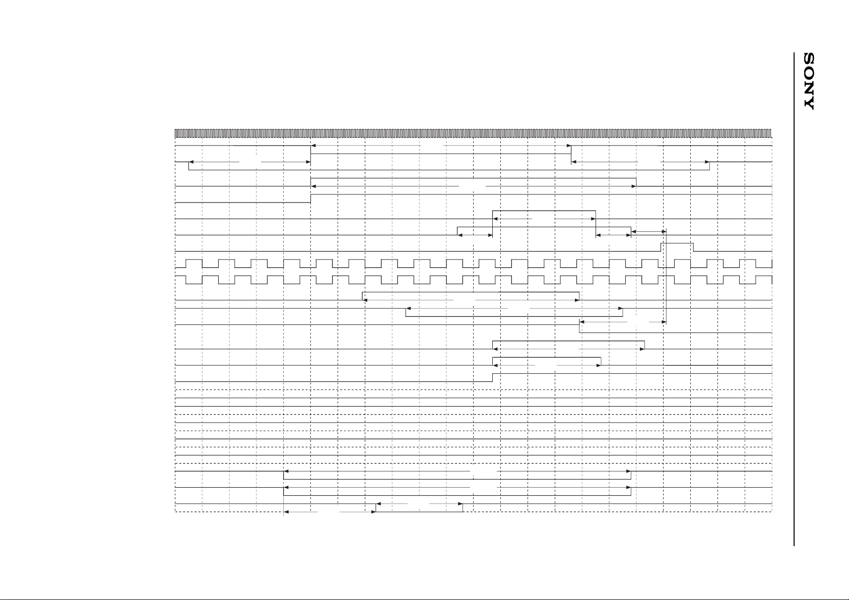
– 95 –
CXD2464R
RGT : H PLLP : LHHLLHHHHHL (LSB) HP : HHLHHHLL (LSB) HSTP : LLLH (LSB) PCGP : LHLLH (LSB) PRGP : LHHLH (LSB)
CLPP : LL (LSB) HPOL : L HDNPOL : H CLPPOL : H PCGPOL : H PRGPOL : H HR : H HST : H PCG : H DSP : H
Loop Counter : 832 clk
MCK f : 40.00MHz (25.00ns)
13 clk
32 clk
MCK
HSYNC
(BLK)
HD
HDN
CLP1
CLP2
HST
HCK1
HCK2
CLR
ENB
VCK
PRG
PCG
FRP
BLK
RSTR
RCK
RSTW
WCK
IRACT
ORACT
XHS
13 clk 13 clk
782 792 802 812 822 0 10 20 30 40 50 60 70 80 90 100 110 120 130 140 150 160 179
45 clk
96 clk
120 clk
51 clk
38 clk
80 clk
80 clk
32 clk
56 clk
40 clk
128 clk
128 clk
34 clk
Note) When RGT is Low, HCK1 and 2 have the same polarity.
The third row of the timing chart (BLK) is a pulse indicated as a reference and is not a pulse output from pins.
LCX012BL SVGA 640 × 480
Page 96
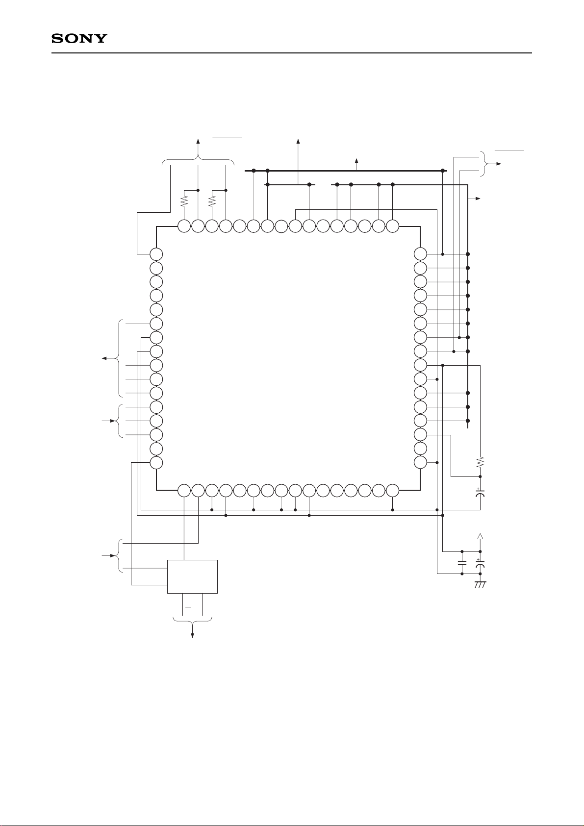
– 96 –
CXD2464R
Application Circuit
100k100k
10k
1µ
/16V
0.1µ
47µ
/16V
+5V
∗
PLL IC
HSYNC
VSYNC
TST0
TST1
TST2
TST3
TST4
V
SS
0
TST5
TST6
TST7
TST8
TST9
TST10
TST11
TST12
SHPD
SHPC
SHPB
SHPA
XFRP
FRP
PRG
CLP2/FLDO
CLP1
HD
DWN
PCG
TST14
VST
VCK
V
SS
2
ENB
CLR
BLK
HCK2
HCK1
HST
XRGT
RGT
V
DD0
V
SS1
MODE1
MODE2
MODE3
XCLR
TST13
CKI2
INV
XVS
XHS
IRACT
ORACT
RSTR
V
SS3
V
DD1
RCK
RSTW
WCK
SCTR
SCLK
SDAT
HDN
CKI1
49
50
51
52
53
54
55
56
57
58
59
60
61
63
64
62
33
34
35
36
37
38
39
40
41
42
43
44
45
46
47
48
17
18
19
20
21
22
23
24
25
26
27
28
29
30
31
32
1
4
5
6
7
8
9
10
11
12
13
14
15
16
CXD2464R
CXD2112R
CXD2112R
Q Q
2
3
S/H driver IC CXA2112R
(when CXA2111R is not used)
LCD signal processing IC
CXA2112R
(when CXA2111R is not used)
LCD panel
Line buffer
µPD485505
Serial I/F
Sync signal
input
∗
PLL IC: Sony CXA3106Q (built-in phase comparator, frequency divider) is recommended.
Application circuits shown are typical examples illustrating the operation of the devices. Sony cannot assume responsibility for
any problems arising out of the use of these circuits or for any infringement of third party patent and other right due to same.
Page 97
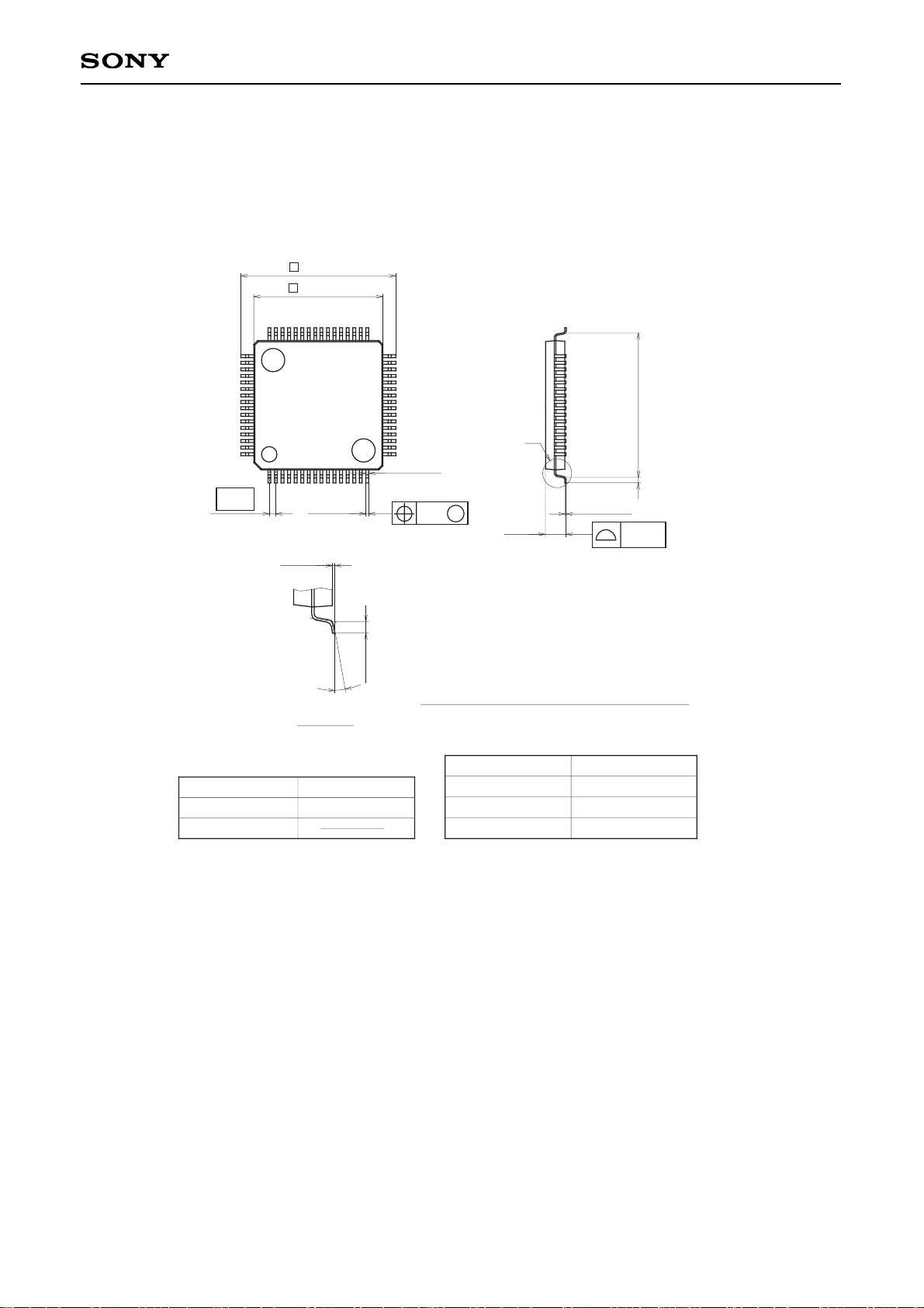
– 97 –
CXD2464R
SONY CODE
EIAJ CODE
JEDEC CODE
PACKAGE MATERIAL
LEAD TREATMENT
LEAD MATERIAL
PACKAGE MASS
EPOXY RESIN
PLATING
42/COPPER ALLOY
PACKAGE STRUCTURE
12.0 ± 0.2
∗ 10.0 ± 0.1
(0.22)
0.18 – 0.03
+ 0.08
1
16
17
32
33
48
49
64
0.1 ± 0.1
0.5 ± 0.2
0° to 10°
64PIN LQFP (PLASTIC)
LQFP-64P-L01
LQFP064-P-1010
0.3g
DETAIL A
0.5 ± 0.2
(11.0)
0.127 – 0.02
+ 0.05
A
1.5 – 0.1
+ 0.2
0.1
SOLDER/PALLADIUM
NOTE: Dimension “∗” does not include mold protrusion.
0.13
M
0.5
Package Outline Unit: mm
 Loading...