

Page 1

Timing Controller for CCD Camera
Description
The CXD2463R generates the sync signals for
timing control and back end signal processing in a
CCD camera system using a 510H or 760H blackand-white CCD image sensor.
Features
• Built-in sync signal generation function
• Built-in electronic iris (electronic shutter) function
• Supports low-speed limiter for electronic iris
• Supports external synchronization
(Line-Lock, VReset + HPLL)
• Supports automatic external sync discrimination
• Window pulse output for backlight compensation
• Built-in V driver
Applications
• Surveillance camera
• Door phone camera
Structure
Silicon gate CMOS IC
Applicable CCD Image Sensors
• Type 1/2, 760H black-and-white CCD (EIA/CCIR)
•
Type 1/3, 510/760H black-and-white CCD (EIA/CCIR)
•
Type 1/4, 510/760H black-and-white CCD (EIA/CCIR)
Absolute Maximum Ratings
• Supply voltage VDD, AVDD
VSS – 0.5 to VSS + 7.0 V
• Supply voltage VSS VL – 0.5 to VL + 26.0 V
• Supply voltage VH VL – 0.5 to VL + 26.0 V
• Supply voltage VM VL – 0.5 to VL + 26.0 V
• Input voltage VI VSS – 0.5 to VDD + 0.5 V
• Output voltage VO VSS – 0.5 to VDD + 0.5 V
• Operating temperature
Topr –20 to +75 °C
• Storage temperature
Tstg –55 to +150 °C
Recommended Operating Conditions
• Supply voltage 1 VDD, AVDD
4.75 to 5.25 V
• Supply voltage 3 VH 14.55 to 15.45 V
• Supply voltage 4 VL –9.0 to –8.0 V
• Supply voltage 5 VM 0 V
• Operating temperature
Topr –20 to +75 °C
Base oscillation
• 1212fH (EIA: 19.0699MHz)
(CCIR: 18.9375MHz)
• 1820fH (EIA: 28.6364MHz)
• 1816fH (CCIR: 28.375MHz)
– 1 –
E98930B9X
Sony reserves the right to change products and specifications without prior notice. This information does not convey any license by
any implication or otherwise under any patents or other right. Application circuits shown, if any, are typical examples illustrating the
operation of the devices. Sony cannot assume responsibility for any problems arising out of the use of these circuits.
CXD2463R
48 pin LQFP (Plastic)
Page 2

– 2 –
CXD2463R
NO SIGNAL
DETECTION
CIRCUIT
VD DETECTION
CIRCUIT
SYNC
DISCRIMINATION
CIRCUIT
GATE
HV-PLL SELECTOR
LCIN
COMP
EVD
EHD/SYNC
EXT
HVDET
VD
HD
EIA
V
DD1
V
DD2
V
SS1
V
SS2
TEST
LCOUT
CKI
CCD
AVSS
H1
H2
AV
DD
RG
SHP
SHD
V1
V2
V3
V4
VL
VM
SUB
VH
SYNC
CBLK
CLP1
CLP2
BLC
BLCW2
BLCW1
CV
SS
IRIN/ED1
SPDNV/ED2
Vreg
CV
DD
SPUPV/ED0
1/2 1/606
1/910
1/908
TG/SSG
RESET
GEN
IRIS/SHUTTER
CK GEN
COUNTER
ESHUT2
ESHUT1
RST
TEST CIRCUIT
SELECTOR
DECODEUP/DOWN ADDER
GATE
VD
IHD
IVD
EIA
HD
40
39
41
42
28
47
45
46
44
48
31
30
6
3
4
2
8
1
7
5 25 26 23 24 15 17 18 12 13 11 10 9
20
21
29
223216431927363533343837
14
1/525
1/625
SYNC
SEP
V DRIVER
DECODER
HV-PLL SELECTOR
Block Diagram
Page 3
– 3 –
CXD2463R
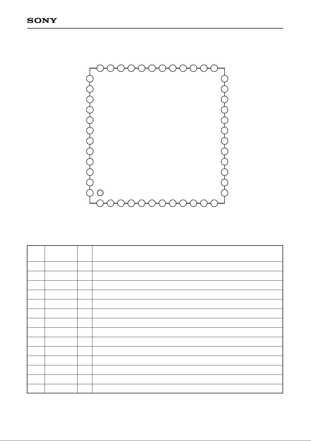
Pin Configuration (Top View)
1 2 3 4 5 6 7 8 9 10 11 12
13
14
15
16
17
18
19
20
21
22
23
24
2526272829
30
313233343536
37
38
39
40
41
42
43
44
45
46
47
48
IRIN/ED1
CVSS
BLC
V
SS1
BLCW1
BLCW2
V
DD1
ESHUT2
ESHUT1
TEST
CLP1
CLP2
SYNC
CBLK
EIA
CCD
RST
SHD
SHP
V
SS2
HVDET
EXT
VD
HD
SPDNV/ED2
SPUPV/ED0
Vreg
CVDD
VL
SUB
V1
VH
V3
V2
V4
VM
RG
AVSS
H2
H1
AV
DD
VDD2
CKI
LCOUT
LCIN
COMP
EHD/SYNC
EVD
Pin Description
Pin
No.
1
2
3
4
5
6
7
8
9
10
11
12
13
14
VM
V4
V2
V3
VH
V1
SUB
VL
CVDD
Vreg
SPUPV/ED0
SPDNV/ED2
IRIN/ED1
CVSS
—
O
O
O
—
O
O
—
—
—
I
I
I
—
Power supply (GND for V driver)
Pulse output for CCD vertical register drive
Pulse output for CCD vertical register drive
Pulse output for CCD vertical register drive
Power supply (positive power supply for V driver)
Pulse output for CCD vertical register drive
CCD discharge pulse output
Power supply (negative power supply for V driver)
Power supply (for comparator)
Bias current supply for comparator
Shutter speed up reference voltage/shutter speed setting
Shutter speed down reference voltage/shutter speed setting
Iris signal input/shutter speed setting
GND (for comparator)
Symbol
I/O Description
Page 4

– 4 –
CXD2463R
Pin
No.
15
16
17
18
19
20
21
22
23
24
25
26
27
28
29
30
31
32
33
34
35
36
37
38
39
40
41
42
43
44
45
46
47
48
BLC
VSS1
BLCW1
BLCW2
VDD1
ESHUT2
ESHUT1
TEST
CLP1
CLP2
SYNC
CBLK
EIA
CCD
RST
SHD
SHP
VSS2
HVDET
EXT
VD
HD
EVD
EHD/SYNC
COMP
LCIN
LCOUT
CKI
VDD2
AVDD
H1
H2
AVSS
RG
O
—
I
I
—
I
I
I
O
O
O
O
I
I
I
O
O
—
O
O
O
O
I
I
O
I
O
I
—
—
O
O
—
O
Window pulse output for backlight compensation
GND
Window select 1 for backlight compensation (with pull-down resistor)
Window select 2 for backlight compensation (with pull-down resistor)
Power supply
Sub pulse control (with pull-down resistor)
Sub pulse control (with pull-down resistor)
Fixed low (with pull-down resistor)
Clamp pulse output
Clamp pulse output
Composite sync output
Composite blanking output
Low: EIA, High: CCIR (with pull-down resistor)
Low: 510H, High: 760H (with pull-down resistor)
Reset (low reset). Always input reset pulse after power-on.
Data sample-and-hold pulse
Precharge level sample-and-hold pulse
GND
Horizontal PLL/Vertical PLL discrimination signal
High: Vertical PLL, Low: Horizontal PLL
External sync/internal sync discrimination signal
High: External sync, Low: Internal sync
Vertical drive output
Horizontal drive output
Vertical drive signal input (with pull-up resistor)
Horizontal drive signal input/Composite sync input (with pull-up resistor)
Comparator output
Inverter input for oscillation
Inverter output for oscillation
2MCK input
Power supply
Power supply (for H1, H2, and RG)
H1 clock output for CCD horizontal register drive
H2 clock output for CCD horizontal register drive
GND (for H1, H2, and RG)
Reset gate pulse output
Symbol I/O Description
Page 5

– 5 –
CXD2463R
Electrical Characteristics
1) DC Characteristics
(VDD = 5V ± 0.25V, Topr = –20 to +75°C)
Item
VDD
VIH1
VIL1
VIH2
VIL2
VIN3
VIN4
VOH1
VOL1
VOH2
VOL2
VOH3
VOL3
VOH4
VOL4
VOH5
VOL5
VOH6
VOL6
VOH7
VOL7
RFE1
RFE2
RPU
RRD
IVM
IVL
IVH
IOH = –4.0mA
IOL = 8.0mA
IOH = –6.9mA
IOL = 3.0mA
IOH = –17.4mA
IOL = 12.0mA
IOH = –6.0mA
IOL = 4.0mA
IOH = –5.0mA
IOL = 10.0mA
IOH = –7.2mA
IOL = 5.0mA
IOH = –4.0mA
IOL = 5.4mA
VIN = VDD or VSS
VIN = VDD or VSS
VIL = 0V
VIH = VDD
AVDD = 5V
CVDD = 5V
VDD1 = 5V
VDD2 = 5V
VL = –8.5V
VH = 15V
4.75
0.7VDD
0.8VDD
2.0
VSS
VDD – 0.8
VDD – 0.8
VDD – 0.8
VDD – 0.8
VM– 0.25
VH– 0.25
VH– 0.25
250k
250k
20k
20k
5.0
1M
1M
50k
50k
24
1.9
0.8
5.25
0.3VDD
0.2VDD
VDD
VDD
0.4
0.4
0.4
0.4
VL+ 0.25
VM+ 0.25
VL
+ 0
.25
2.5M
2.5M
125k
125k
V
V
V
V
V
V
V
V
V
V
V
V
V
V
V
V
V
V
V
V
V
Ω
Ω
Ω
Ω
mA
mA
mA
Symbol Conditions Min. Typ. Max. Unit
Supply voltage
Input voltage 1
(For input pins not listed below)
Input voltage 2
(Pin 29)
Input voltage 3
(Pins 11 and 12 in electronic iris
mode)
Input voltage 4
(Pin 13 in electronic iris mode)
Output voltage 1
(Pins 15, 23, 24, 25, 26, 33, 34, 35 and 36)
Output voltage 2
(Pins 30, 31 and 48)
Output voltage 3
(Pins 45 and 46)
Output voltage 4
(Pin 39)
Output voltage 5
(Pins 2, 3, 4 and 6)
Output voltage 6
(Pins 4 and 6 (SG))
Output voltage 7
(Pin 7)
Feedback resistor 1
(Pin 42)
Feedback resistor 2
(Resistor between Pins 40 and 41)
Pull-up resistor
Pull-down resistor
Current consumption
∗
The typical power consumption is 148mW with the ICX054BL load (in the normal operating state).
Page 6

– 6 –
CXD2463R
2) Input/Output Capacitance (VDD = VI = 0V, fM = 1MHz)
Item
Input pin capacitance
Output pin capacitance
I/O pin capacitance
CIN
COUT
CI/O
9
11
11
pF
pF
pF
Symbol Min. Typ. Max. Unit
3) Comparator Characteristics (VDD = 5V ± 0.25V, Topr = –20 to +75°C)
Item
Indefinite region Vf ±70 mV
Symbol Min. Typ. Max. Unit
4) Power-on Reset Condition
(Within the recommended operating condition)
Item
Power-on reset period
tWRST
35 ns
Symbol Min. Typ. Max. Unit
Note 1) Input offset voltage and indefinite region
The input offset voltage and indefinite region (region in which the comparator output is not set to high
or low) shown in the figure below exist in the built-in comparator in this IC, so be careful when
designing the external circuit.
Note 2) Pins 11 and 12 in electronic iris mode
Make sure of Pin 11 (SPUPV) < Pin 12 (SPDNV).
5.0V
GND
70mV
70mV
Pins 11 and 12
(SPUPV, SPDNV)
Indefinite region
4.75V
tWRST
0.2VDD
VDD
RST
Page 7

– 7 –
CXD2463R
1. Electronic Iris/Electronic Shutter Function
The electronic iris or electronic shutter can be selected by setting the following pins to different combinations of
high and low.
ESHUT1
Pin 21
L
H
L
H
L
L
H
H
Electronic iris without limiter
Electronic iris with limiter EIA: 1/100 (s), CCIR: 1/120 (s)
Electronic shutter mode
Sub pulse stopped
ESHUT2
Pin 20
Operating Mode
Symbol
IRIN/ED1
SPDNV/ED2
SPUPV/ED0
13
12
11
Iris signal input
Shutter speed down reference voltage
Shutter speed up reference voltage
Pin No. Function
1) Electronic Iris Mode
Symbol
SPUPV/ED0
IRIN/ED1
SPDNV/ED2
Shutter speed
11
13
12
H
H
H
EIA:
1/100
CCIR:
1/120
L
H
H
1/250
H
L
H
1/500
L
L
H
1/1000
H
H
L
1/2000
L
H
L
1/5000
H
L
L
1/10000
L
L
L
1/100000
Pin No.
Mode
2) Electronic Shutter Mode
Page 8

– 8 –
CXD2463R
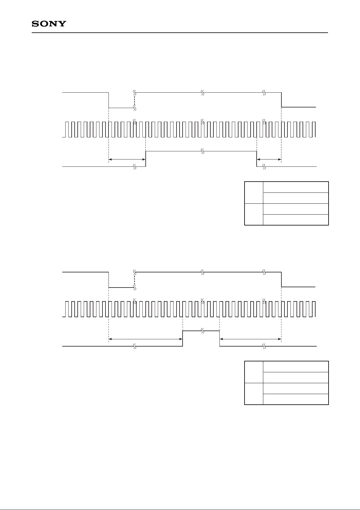
2. Backlighting Correction Function
The CXD2463R has a function to output the window pulse for backlight compensation.
The backlight compensation pulse is output from BLC (Pin 15) in the following range according to the high/low
combination of BLCW1 (Pin 17) and BLCW2 (Pin 18).
Window Type for Different Pin Combinations
Window type
Full-screen photometry
Bottom emphasis photometry
Center emphasis photometry
Bottom + center emphasis photometry
L
H
L
H
L
L
H
H
BLCW1 (Pin 17) BLCW2 (Pin 18)
Example of Basic Circuit Configuration
Iris comparator
Iris
window switch
AGC
window switch
IRIN/ED1
13
BLC
3.9k
10k
39k
+5V
100k 10µ
IRIS
OP+
DETOUT
1k10k
100k
10µ
10k
10k
CXD2463R CXA1310AQ
15
27
19
13
Full-screen photometry
Center emphasis photometry
Bottom emphasis photometry
Bottom + center emphasis photometry
Page 9

– 9 –
CXD2463R
1) Window Pulse Timing Charts
• EIA Mode/Vertical Direction Timing
(1) Full-screen photometry
VD
HD
BLC
20HD
20.5HD
0.5HD
(2) Center emphasis photometry
VD
HD
BLC
181HD
101HD
181.5HD
101.5HD
(3) Bottom emphasis photometry
VD
HD
BLC
181HD
181.5HD
0.5HD
Page 10
– 10 –
CXD2463R
• EIA Mode/Horizontal Direction Timing
(1) Bottom emphasis photometry and full-screen photometry
HD
MCK
BLC
X1
X2
X1
510H
760H
510H
760H
104MCK
154MCK
3MCK
22MCK
X2
(2) Center emphasis photometry
HD
MCK
BLC
X1
X2
X1
510H
760H
510H
760H
272MCK
407MCK
167MCK
252MCK
X2
Page 11

– 11 –
CXD2463R
• CCIR Mode/Vertical Direction Timing
(1) Full-screen photometry
VD
HD
BLC
25HD
25.5HD
0.5HD
(2) Center emphasis photometry
VD
HD
BLC
216HD
121HD
216.5HD
121.5HD
(3) Bottom emphasis photometry
VD
HD
BLC
216HD
216.5HD
0.5HD
Page 12

– 12 –
CXD2463R
• CCIR Mode/Horizontal Direction Timing
(1) Bottom emphasis photometry and full-screen photometry
HD
MCK
BLC
X1
X2
X1
510H
760H
510H
760H
114MCK
169MCK
3MCK
22MCK
X2
(2) Center emphasis photometry
HD
MCK
BLC
X1
X2
X1
510H
760H
510H
760H
279MCK
416MCK
164MCK
246MCK
X2
Page 13
– 13 –
CXD2463R
3. External Sync Function
The CXD2463R supports the three modes of Line-Lock, VReset + HPLL (VD and HD inputs), and VReset +
HPLL (Sync input) as the external sync functions. Each mode is automatically switched according to the
combination of signals input to EHD/SYNC (Pin 38) and EVD (Pin 37).
1) Automatic External Sync Discrimination
I/O
I
I
O
O
EHD/SYNC
EVD
HVDET
EXT
38
37
33
34
HD
No signal
L
L
INT
No signal
VD
H
H
LL
HD
VD
L
H
VReset
+ HPLL
SYNC
HD after SYNC
separation
L
H
VReset
+ HPLL
No signal
No signal
L
L
INT
Symbol
Pin
No.
EHD/SYNC and EVD pins signal input state
and HVDET and EXT pins discrimination results
Mode
• If unspecified signals are input for the external signals given above, there may be recognition errors.
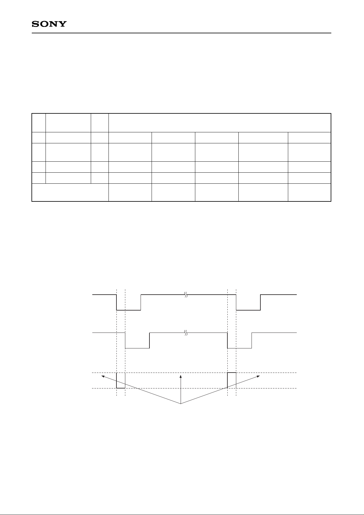
2) LL (Line-Lock) Mode
When the V sync clock is externally input to EVD (Pin 37), the result of comparing the falling edge of the clock
and the falling edge of the internal VD is output from COMP (Pin 39). The output polarity is compatible with the
active filter.
EXT-VD
(Pin 37)
INT-VD
(Pin 35)
COMP
(Pin 39)
High impedance state
Page 14
– 14 –
CXD2463R
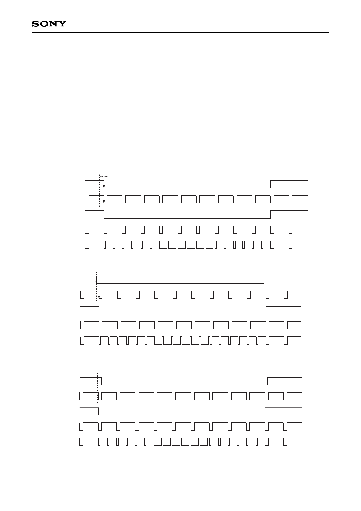
3) VReset + HPLL (VD and HD Inputs) Mode
When the HD cycle clock is externally input to EHD/SYNC (Pin 38) and the V cycle clock is externally input to
the EVD (Pin 37), the CXD2463R sync signal is output as shown below based on the phase difference
between these signals.
Similar to Line-Lock mode, the result of comparing the phase of the falling edges of the HD cycle clock input to
Pin 38 and the CXD2463R internal HD is output from COMP (Pin 39). The PLL is applied using this signal.
Similar to Line-Lock mode, the polarity of the COMP (Pin 39) output is compatible with the active filter. The
phase of the HD falling edge can be shifted up to ±1/4H with respect to the falling edge of the master VD (EXTVD).
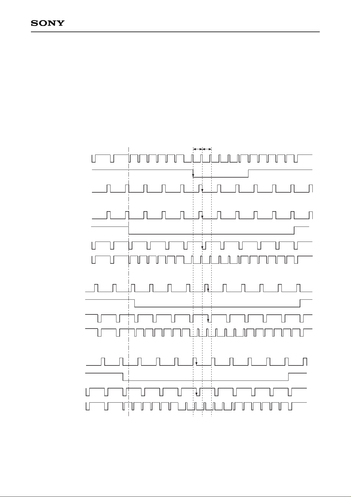
• EIA/ODD
(1) EXT-VD and EXT-HD have the same phase.
1/4H1/4H
EXT-VD
(Pin 37 input)
EXT-HD
(Pin 38 input)
VD
(Pin 35 output)
HD
(Pin 36 output)
SYNC
(Pin 25 output)
(2) EXT-VD and EXT-HD have the same phase to +1/4H.
EXT-VD
EXT-HD
VD
HD
SYNC
(3) EXT-VD and EXT-HD have the –1/4H to the same phase.
EXT-VD
EXT-HD
VD
HD
SYNC
Page 15

– 15 –
CXD2463R
• EIA/EVEN
(1) EXT-VD and EXT-HD have the same phase.
1/4H1/4H
EXT-VD
(Pin 37 input)
EXT-HD
(Pin 38 input)
VD
(Pin 35 output)
HD
(Pin 36 output)
SYNC
(Pin 25 output)
(2) EXT-VD and EXT-HD have the same phase to +1/4H.
EXT-VD
EXT-HD
VD
HD
SYNC
(3) EXT-VD and EXT-HD have the same phase to –1/4H.
EXT-VD
EXT-HD
VD
HD
SYNC
Page 16

– 16 –
CXD2463R
• CCIR/ODD
(1) EXT-VD and EXT-HD have the same phase.
1/4H1/4H
EXT-VD
(Pin 37 input)
EXT-HD
(Pin 38 input)
VD
(Pin 35 output)
HD
(Pin 36 output)
SYNC
(Pin 25 output)
(2) EXT-VD and EXT-HD have the same phase to +1/4H.
EXT-VD
EXT-HD
VD
HD
SYNC
(3) EXT-VD and EXT-HD have the same phase to –1/4H.
EXT-VD
EXT-HD
VD
HD
SYNC
Page 17

– 17 –
CXD2463R
• CCIR/EVEN
(1) EXT-VD and EXT-HD have the same phase.
1/4H1/4H
EXT-VD
(Pin 37 input)
EXT-HD
(Pin 38 input)
VD
(Pin 35 output)
HD
(Pin 36 output)
SYNC
(Pin 25 output)
(2) EXT-VD and EXT-HD have the same phase to +1/4H.
EXT-VD
EXT-HD
VD
HD
SYNC
(3) EXT-VD and EXT-HD have the same phase to –1/4H.
EXT-VD
EXT-HD
VD
HD
SYNC
Page 18
– 18 –
CXD2463R
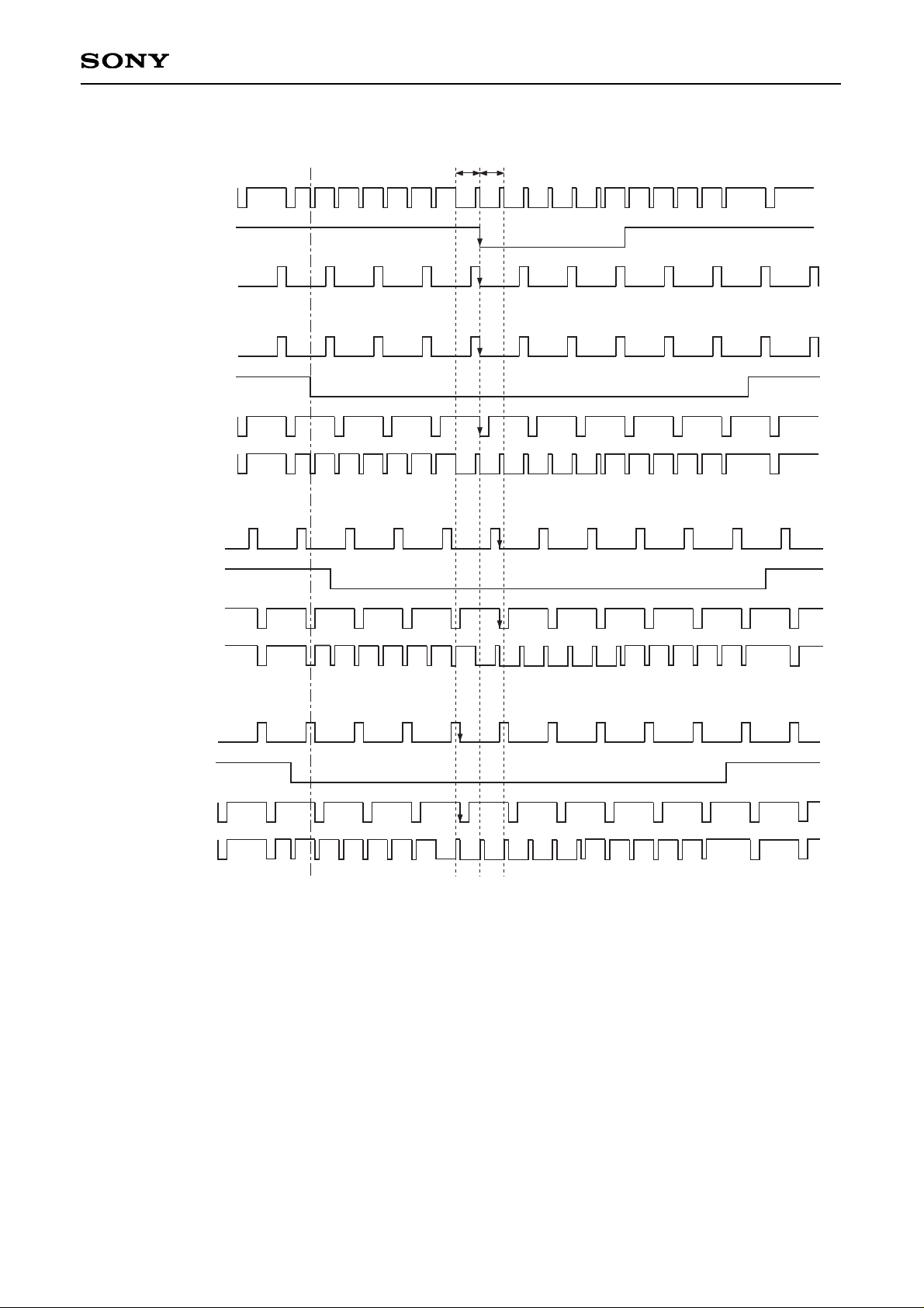
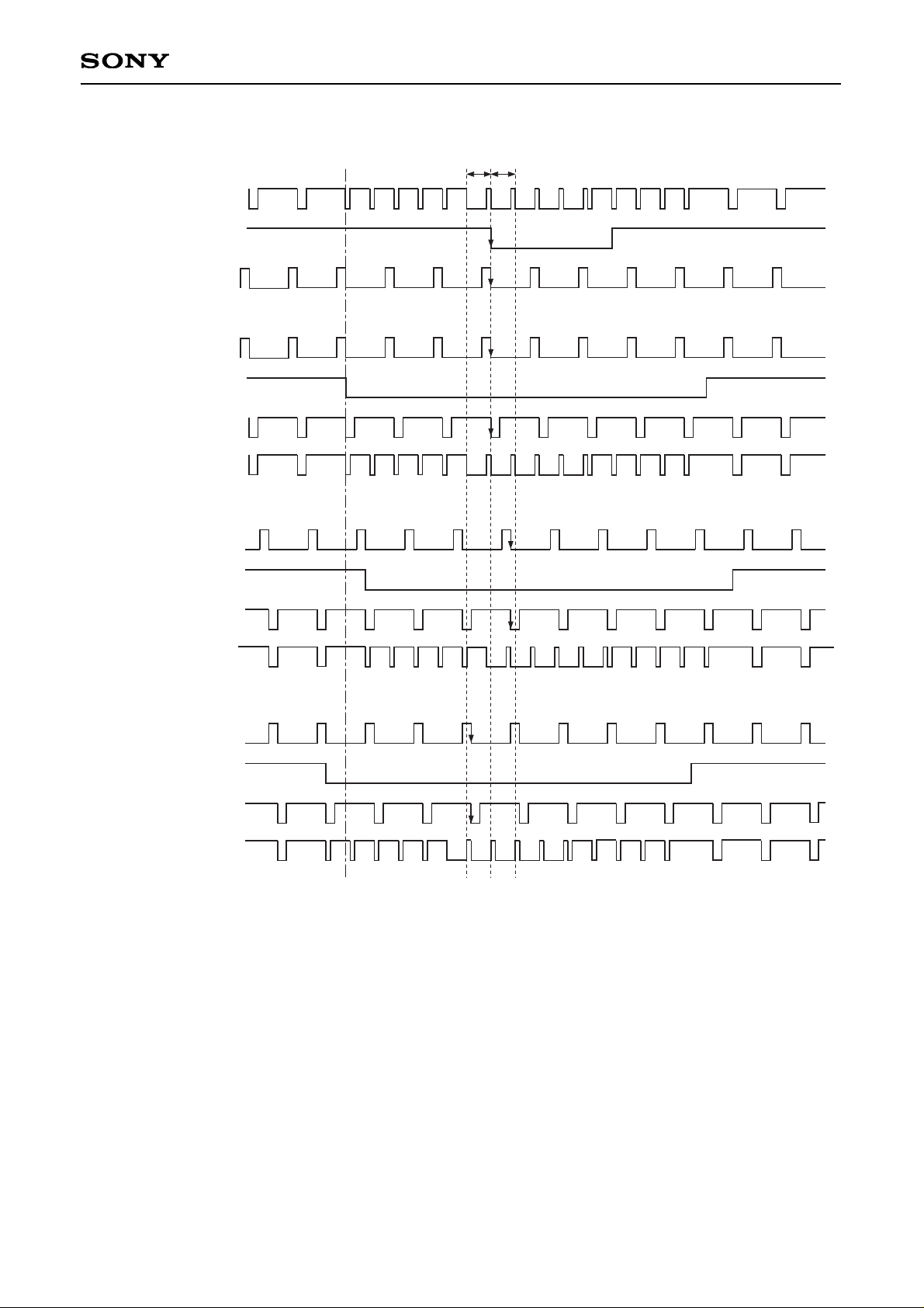
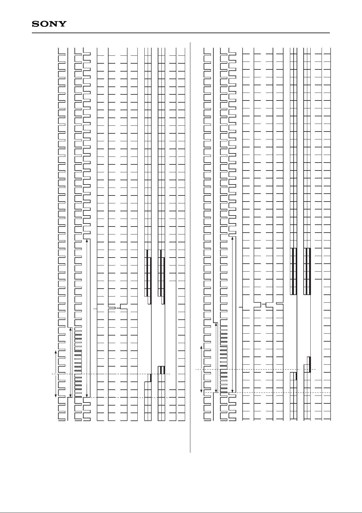
4) VReset + HPLL (SYNC Input) Mode
When the specified sync signal is externally input to EHD/SYNC (Pin 38), the EXT-HD separated from this
sync signal is output from HD (Pin 36). This signal is input through the shifter to EVD (Pin 37). At this time, the
CXD2463R sync signal is output as shown below based on the amount by which EXT-HD is shifted. (The
phase can be shifted up to ±1/2H with respect to the falling edge of EXT-HD.)
COMP (Pin 39) outputs the result of comparing the phase of the falling edge of the shifted EXT-HD (signal
input to Pin 37) and the falling edge of the CXD2463R internal HD. The polarity is compatible with the active
filter.
• EIA/ODD
EXT-HD
(Pin 36 output)
(1) Same phase
(2) Delayed phase
EXT-VD
(Generated inside
the CXD2463R)
HD
(Generated inside
the CXD2463R)
EXT-SYNC
(Pin 38 input)
∗
SFT-HD (1) to (3) are the signals after shifting EXT-HD.
1/2H 1/2H
VD
(Pin 35 output)
SFT-HD (1)
(Pin 37 input)
SFT-HD (2)
VD
HD
SYNC
(3) Advanced phase
SFT-HD (3)
VD
HD
SYNC
SYNC
(Pin 25 output)
Page 19
– 19 –
CXD2463R
• EIA/EVEN
EXT-HD
(Pin 36 output)
(1) Same phase
(2) Delayed phase
EXT-VD
(Generated inside
the CXD2463R)
HD
(Generated inside
the CXD2463R)
EXT-SYNC
(Pin 38 input)
1/2H 1/2H
VD
(Pin 35 output)
SFT-HD (1)
(Pin 37 input)
SFT-HD (2)
VD
HD
SYNC
(3) Advanced phase
SFT-HD (3)
VD
HD
SYNC
SYNC
(Pin 25 output)
Page 20

– 20 –
CXD2463R
• CCIR/ODD
EXT-HD
(Pin 36 output)
(1) Same phase
(2) Delayed phase
EXT-VD
(Generated inside
the CXD2463R)
HD
(Generated inside
the CXD2463R)
EXT-SYNC
(Pin 38 input)
1/2H 1/2H
VD
(Pin 35 output)
SFT-HD (1)
(Pin 37 input)
SFT-HD (2)
VD
HD
SYNC
(3) Advanced phase
SFT-HD (3)
VD
HD
SYNC
SYNC
(Pin 25 output)
Page 21
– 21 –
CXD2463R
• CCIR/EVEN
EXT-HD
(Pin 36 output)
(1) Same phase
(2) Delayed phase
EXT-VD
(Generated inside
the CXD2463R)
HD
(Generated inside
the CXD2463R)
EXT-SYNC
(Pin 38 input)
1/2H 1/2H
VD
(Pin 35 output)
SFT-HD (1)
(Pin 37 input)
SFT-HD (2)
VD
HD
SYNC
(3) Advanced phase
SFT-HD (3)
VD
HD
SYNC
SYNC
(Pin 25 output)
Page 22
– 22 –
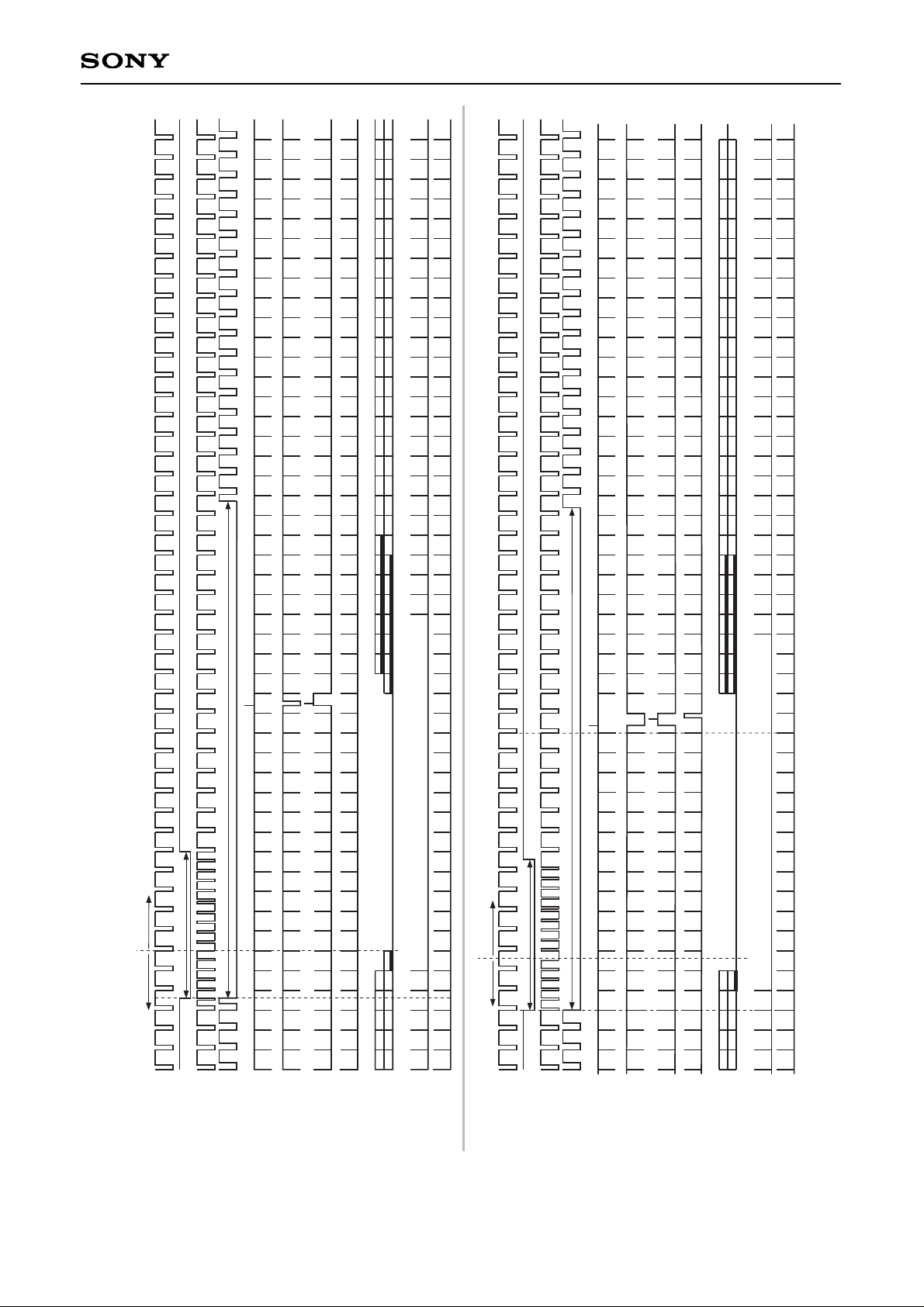
CXD2463R
HD
FIELD.O FIELD.E
VD
SYNC
BLK
V1
V2
V3
V4
510H
CCD OUT
760H
CCD OUT
CLP1
1324132
4
492
493
492
493
CLP2
9H
20H
494
HD
FIELD.E FIELD.O
VD
SYNC
BLK
V1
V2
V3
V4
510H
CCD OUT
760H
CCD OUT
CLP1
491
2
493
492
1 3
1 3
2
493
494
CLP2
9H
20H
Timing Generator + Sync Generator Block Timing Chart
Vertical Direction EIA (during 510H/760H CCD drive)
Page 23
– 23 –
CXD2463R
HD
FIELD.E FIELD.O
VD
SYNC
BLK
V1
V2
V3
V4
510H
CCD OUT
581
582
583
2
1 3
7.5H
25H
HD
FIELD.O FIELD.E
VD
SYNC
BLK
7.5H
25H
132
4
582
583
V1
V2
V3
V4
510H
CCD OUT
CLP1
CLP2
CLP1
CLP2
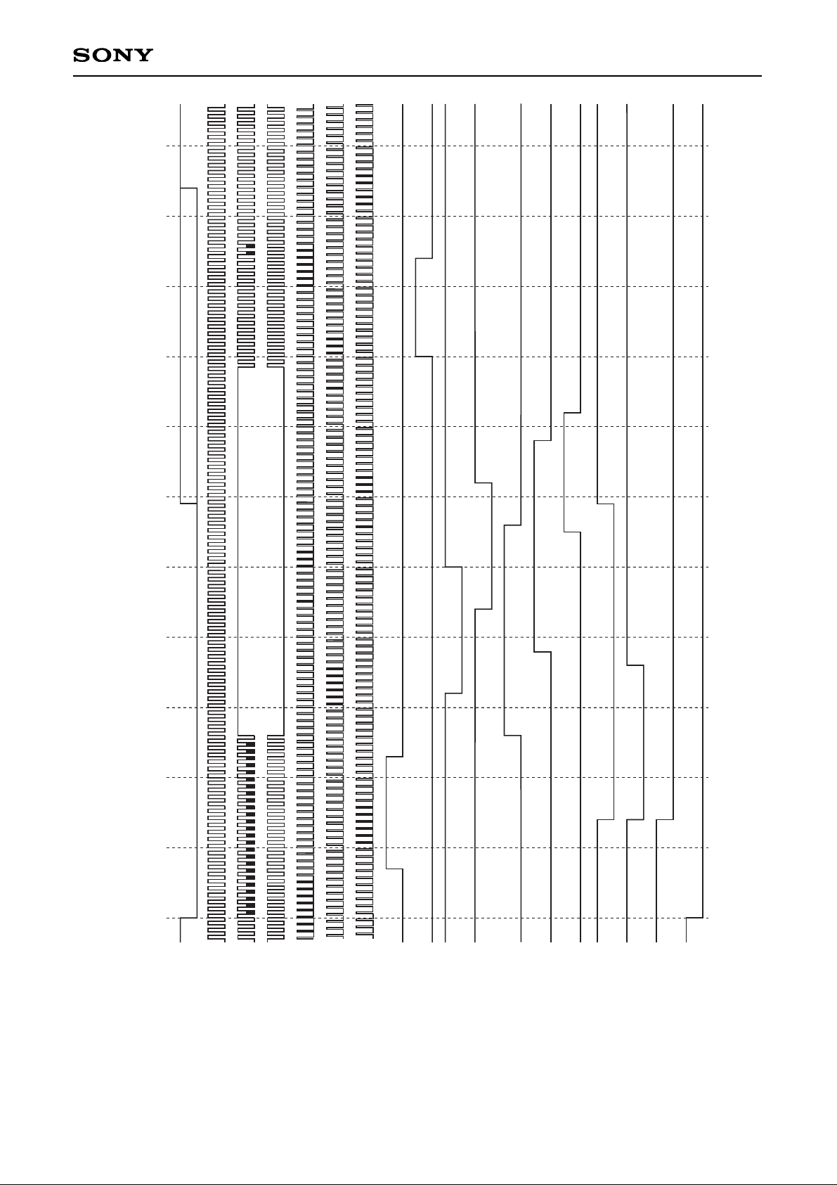
Timing Generator + Sync Generator Block Timing Chart
Vertical Direction CCIR (during 510H CCD drive)
Page 24

– 24 –
CXD2463R
HD
FIELD.E FIELD.O
VD
SYNC
BLK
V1
V2
V3
V4
760H
CCD OUT
581
582
583
2
1 3
7.5H
25H
HD
FIELD.O FIELD.E
VD
SYNC
BLK
7.5H
25H
1
2
582
583
V1
V2
V3
V4
760H
CCD OUT
CLP1
CLP2
CLP1
CLP2
Timing Generator + Sync Generator Block Timing Chart
Vertical Direction CCIR (during 760H CCD drive)
Page 25
– 25 –
CXD2463R
HD/BLK
MCK
(Internal clock)
H1
H2
RG
SHP
SHD
V1
V2
V3
V4
SUB
HSYNC
EQ
VSYNC
VD
CLP1
CLP2
0 10 20 30 40 50 60 70 80 90 100 110
104
MCK = 104.88ns
59
7926
80 94
5032
62 44
56 26
68 38
72 55
5914
3614
14
237
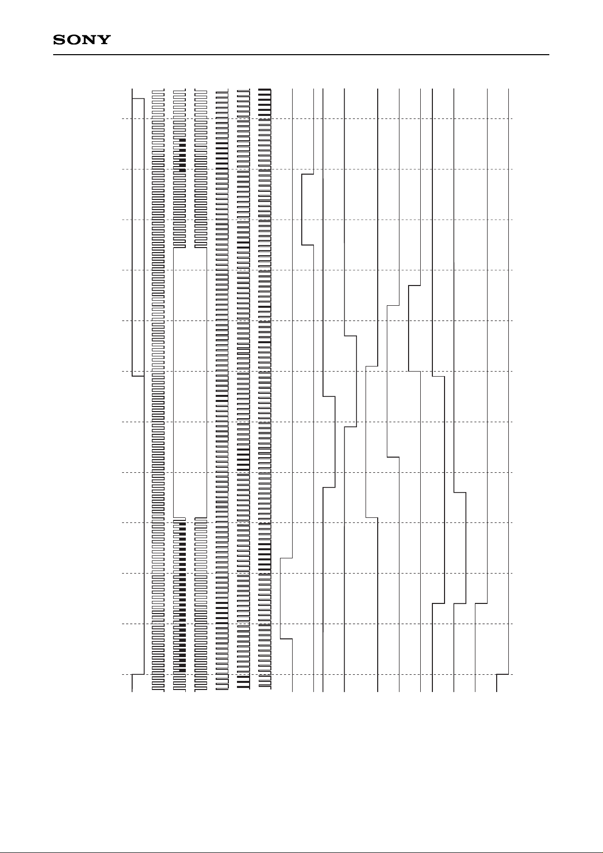
Timing Generator + Sync Generator Block Timing Chart
Horizontal Direction EIA (during 510H CCD drive)
Page 26
– 26 –
CXD2463R
HD/BLK
MCK
(Internal clock)
H1
H2
RG
SHP
SHD
V1
V2
V3
V4
SUB
HSYNC
EQ
VSYNC
VD
CLP1
CLP2
0 10 20 30 40 50 60 70 80 90 100 110
11459
8431
85 99
5537
6749
6131
7343
7760
5914
3614
14
237
MCK = 105.61ns
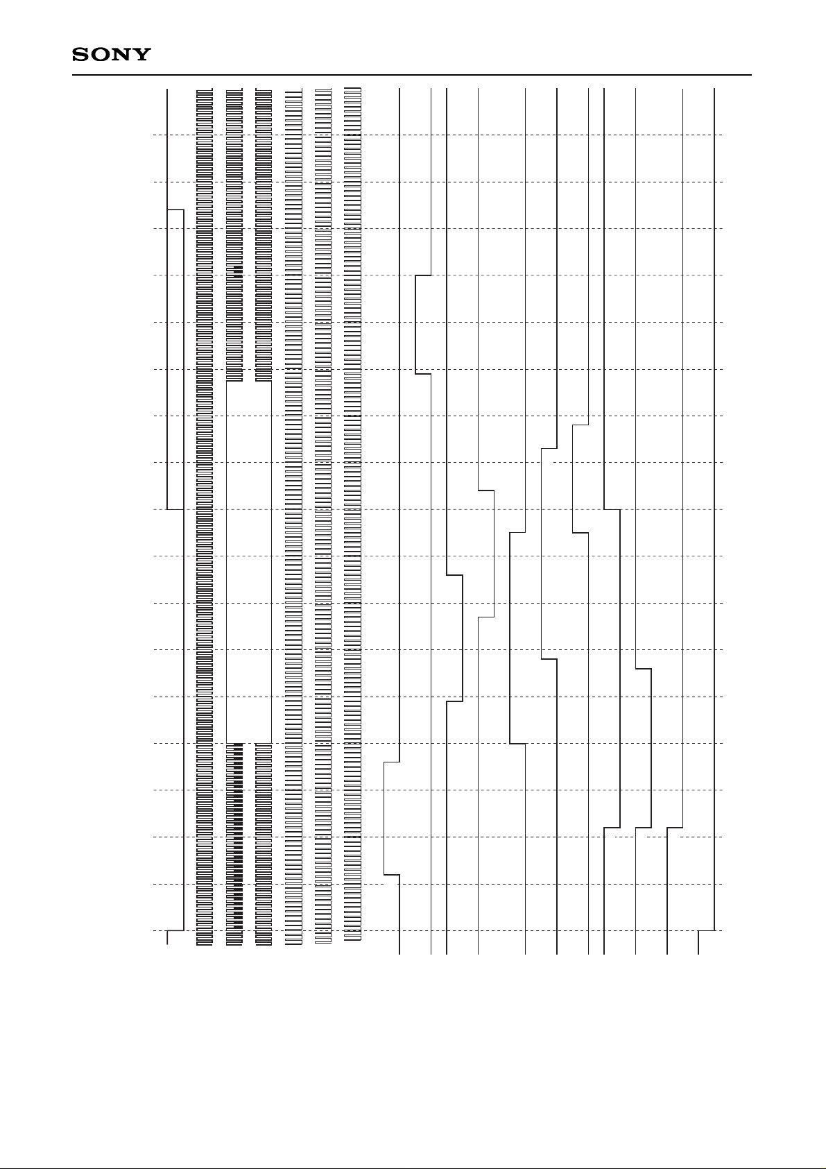
Timing Generator + Sync Generator Block Timing Chart
Horizontal Direction CCIR (during 510H CCD drive)
Page 27
– 27 –
CXD2463R
0 10 20 9080 140 150 160 17010060504030 70 110 120 130
15490
40
118
3612
140119
7649
9467
8540
10358
10885
9022
5622
22
HD/BLK
MCK
(Internal clock)
H1
H2
RG
SHP
SHD
V1
V2
V3
V4
SUB
HSYNC
EQ
VSYNC
VD
CLP1
CLP2
MCK = 69.84ns
Timing Generator + Sync Generator Block Timing Chart
Horizontal Direction EIA (during 760H CCD drive)
Page 28
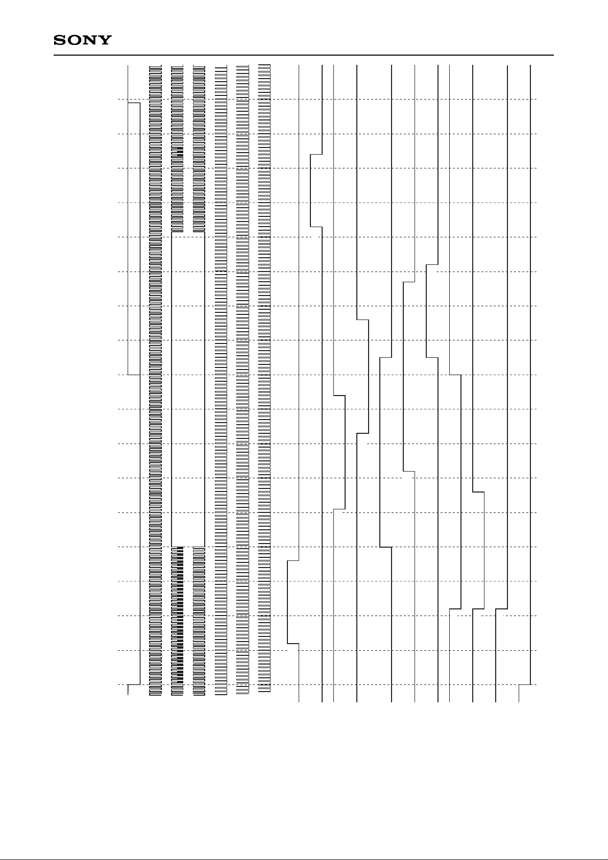
– 28 –
CXD2463R
0 10 20 9080 140 150 160 17010060504030 70 110 120 130
16990
40
132
3612
154
8451
10673
9540
11762
12295
9022
5622
22
HD/BLK
MCK
(Internal clock)
H1
H2
RG
SHP
SHD
V1
V2
V3
V4
SUB
HSYNC
EQ
VSYNC
VD
CLP1
CLP2
MCK = 70.48ns
133
Timing Generator + Sync Generator Block Timing Chart
Horizontal Direction CCIR (during 760H CCD drive)
Page 29
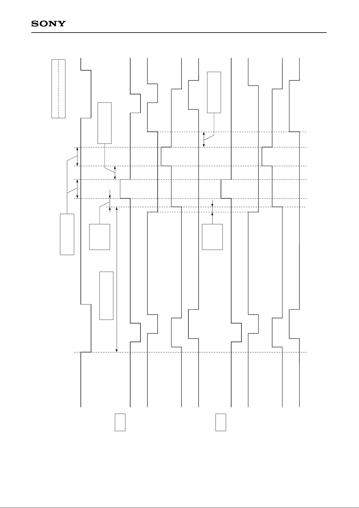
– 29 –
CXD2463R
HD
E: 2.51µs
C: 2.53µs
(24CK)
V1
ODD
V2
V3
V4
V1
EVEN
V2
V3
V4
E: 1.57µs
C: 1.58µs
(15CK)
E: 1.99µs
C: 2.00µs
(19CK)
E: EIA 1CK = 104.88ns
C: CCIR 1CK = 105.61ns
E: 38.38µs
C: 38.65µs
(366CK)
(12CK)
E: 1.26µs
C: 1.27µs
(3CK)
E: 0.32µs
C: 0.32µs
Timing Generator + Sync Generator Block Timing Chart
Charge Readout Timing
Field Accumulation (during 510H CCD drive)
Page 30
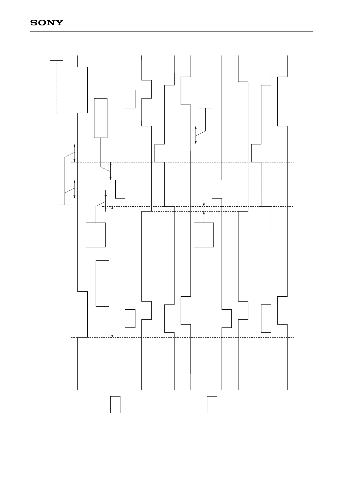
– 30 –
CXD2463R
HD
E: 2.51µs
C: 2.54µs
(36CK)
V1
ODD
V2
V3
V4
V1
EVEN
V2
V3
V4
E: 2.51µs
C: 2.54µs
(36CK)
E: 2.51µs
C: 2.54µs
(36CK)
E: EIA 1CK = 69.84ns
C: CCIR 1CK = 70.48ns
E: 40.56µs
C: 40.95µs
(581CK)
(23CK)
E: 1.61µs
C: 1.62µs
(3CK)
E: 0.21µs
C: 0.21µs
Timing Generator + Sync Generator Block Timing Chart
Charge Readout Timing
Field Accumulation (during 760H CCD drive)
Page 31
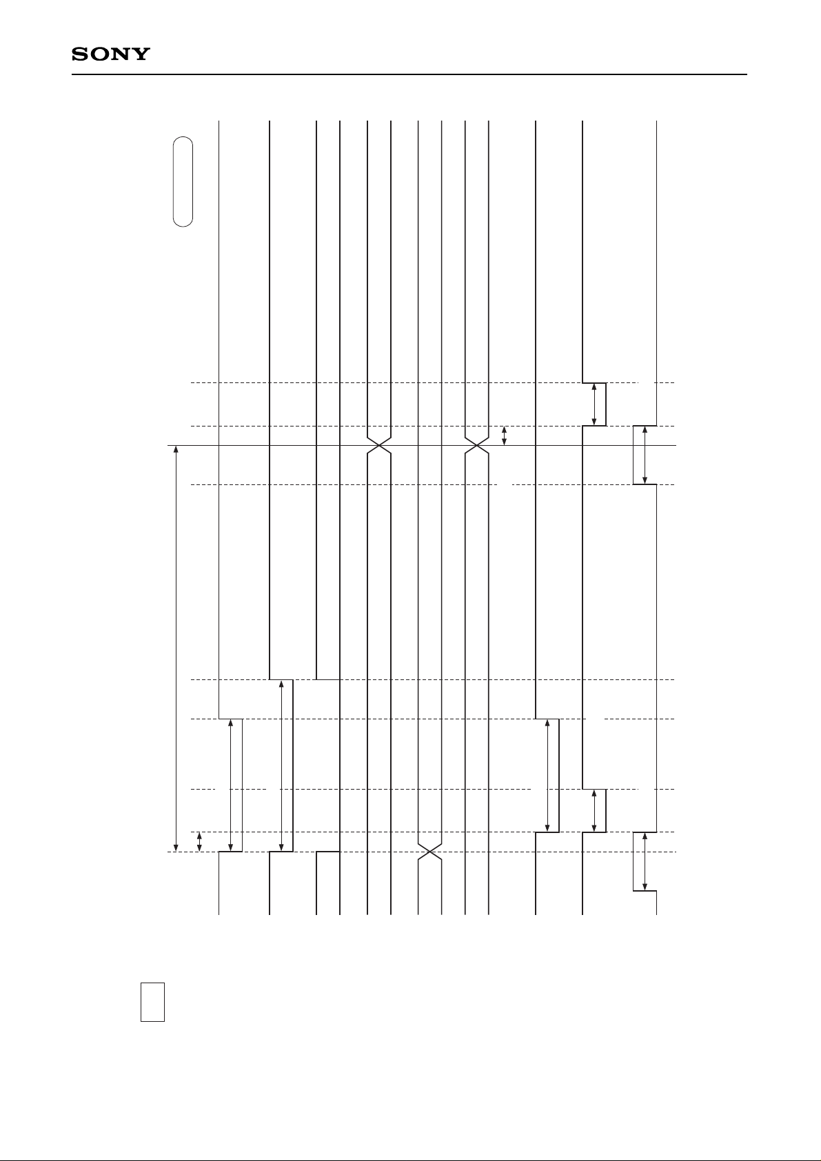
– 31 –
CXD2463R
HD
31.78µs (303CK)
1.47µs (14CK)
1/2H
EIA
HSYNC
EQ
VSYNC
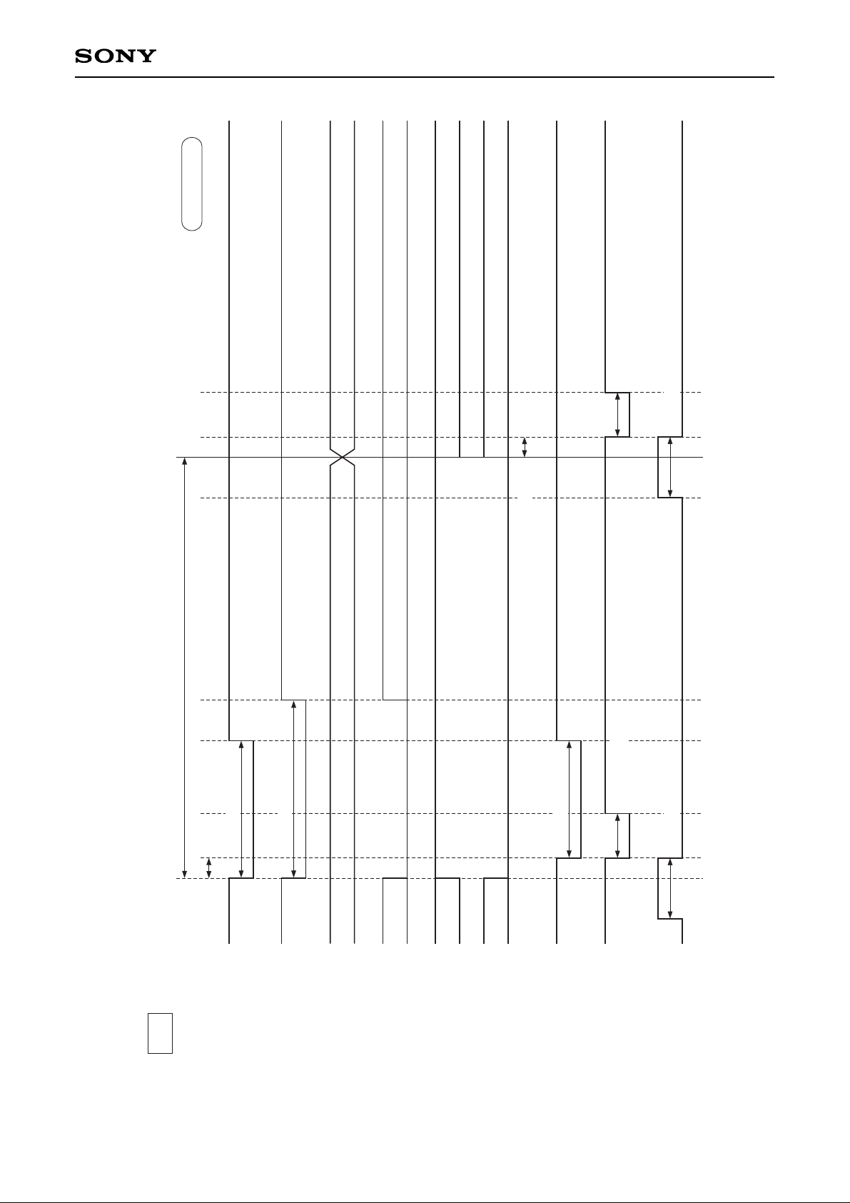
BLK (HD)
BLK (ODD)
BLK (EVEN)
VD (EVEN)
VD (ODD)
6.19µs (59CK)
4.72µs (45CK)
2.30µs (22CK)
4.72µs (45CK)
2.30µs (22CK)
1.47µs (14CK)
1CK = 104.88ns
4.72µs (45CK)
10.90µs (104CK)
Timing Generator + Sync Generator Block Timing Chart
Effective Horizontal Period (during 510H CCD drive)
Page 32
– 32 –
CXD2463R
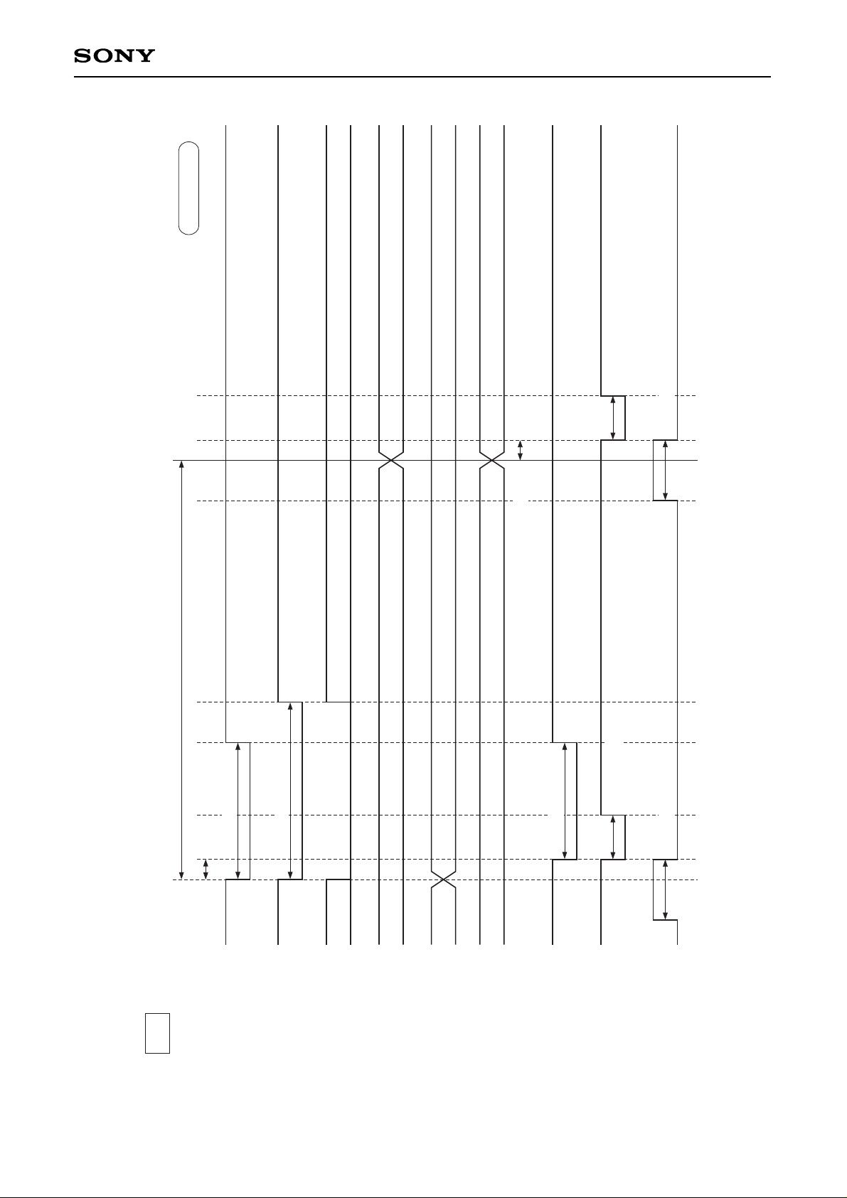
HD
32.00µs (303CK)
1.48µs (14CK)
1/2H
CCIR
HSYNC
EQ
VSYNC
BLK (HD)
BLK (ODD)
VD (EVEN)
VD (ODD)
BLK (EVEN)
6.23µs (59CK)
4.75µs (45CK)
2.30µs (22CK)
4.75µs (45CK)
2.30µs (22CK)
1.48µs (14CK)
1CK = 105.61ns
4.75µs (45CK)
12.04µs (114CK)
Timing Generator + Sync Generator Block Timing Chart
Effective Horizontal Period (during 510H CCD drive)
Page 33
– 33 –
CXD2463R
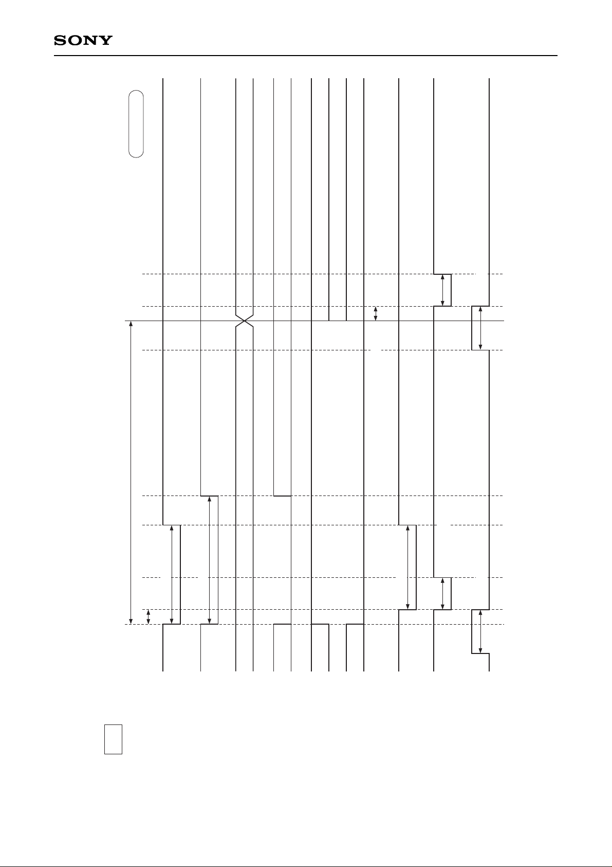
HD
31.78µs (455CK)
1.54µs (22CK)
1/2H
EIA
HSYNC
EQ
VSYNC
BLK (HD)
BLK (ODD)
BLK (EVEN)
VD (EVEN)
VD (ODD)
6.29µs (90CK)
4.75µs (68CK)
2.37µs (34CK)
4.75µs (68CK)
2.37µs (34CK)
1.54µs (22CK)
1CK = 69.84ns
4.75µs (68CK)
10.76µs (154CK)
Timing Generator + Sync Generator Block Timing Chart
Effective Horizontal Period (during 760H CCD drive)
Page 34
– 34 –
CXD2463R
HD
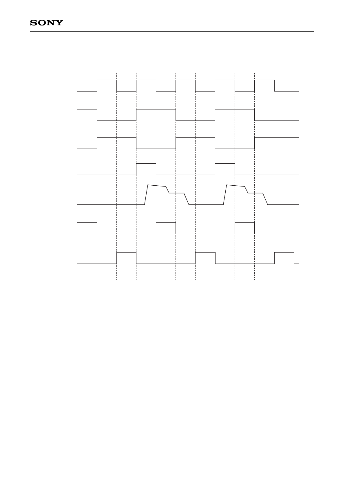
32.00µs (454CK)
1.55µs (22CK)
1/2H
CCIR
HSYNC
EQ
VSYNC
BLK (HD)
BLK (ODD)
VD (EVEN)
VD (ODD)
BLK (EVEN)
6.34µs (90CK)
4.79µs (68CK)
2.40µs (34CK)
4.79µs (68CK)
2.40µs (34CK)
1.55µs (22CK)
1CK = 70.48ns
4.79µs (68CK)
11.91µs (169CK)
Timing Generator + Sync Generator Block Timing Chart
Effective Horizontal Period (during 760H CCD drive)
Page 35
– 35 –
CXD2463R
H1
H2
RG
CCD OUT
MCK
(Internal clock)
SHP
SHD
High-Speed Phase Timing Chart for the Timing Generator Block
Page 36

– 36 –
CXD2463R
VSUB ADJ
36k 50k 50k
10k
3.9k
100
+5V
100
10k
10µ
VIDEO OUT
CCD OUT
10µ
100k
10k
–9.0 to –8.0V
+14.55 to +15.45V
Reset circuit
H shifter
RG ADJ
1000p
10p
10k
10k
10k100k
1000p
1M
0.01µ
SYNC IN
0.1µ
1M
1p
39k
CXA1310AQ
CXD2463R
13
14
15
16
17
18
19
20
21
22
23
24
252627282930313233343536
37
38
39
40
41
42
43
44
45
46
47
48
1 2
3 4 5 6 7 8 9 10
11 12
25
30
27
242021294
510H/760H black-and-white CCD
Application Circuit
• SYNC input external synchronization
• Electronic iris mode
Application circuits shown are typical examples illustrating the operation of the devices. Sony cannot assume responsibility for
any problems arising out of the use of these circuits or for any infringement of third party patent and other right due to same.
Page 37
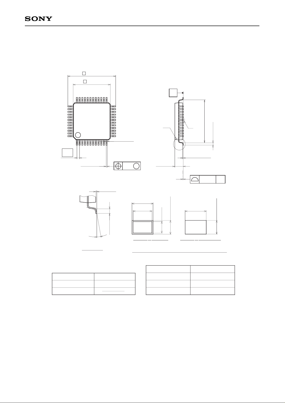
– 37 –
CXD2463R
SONY CODE
EIAJ CODE
JEDEC CODE
PACKAGE MATERIAL
LEAD TREATMENT
LEAD MATERIAL
PACKAGE MASS
EPOXY RESIN
PLATING
42/COPPER ALLOY
PACKAGE STRUCTURE
48PIN LQFP (PLASTIC)
9.0 ± 0.2
∗ 7.0 ± 0.1
1
12
13
24
25
36
37
48
(0.22)
0.18 – 0.03
+ 0.08
0.2g
LQFP-48P-L01
LQFP048-P-0707
(8.0)
0.5 ± 0.2
0.127 – 0.02
+ 0.05
A
1.5 – 0.1
+ 0.2
0.1
SOLDER/PALLADIUM
NOTE: Dimension “∗” does not include mold protrusion.
0.1 ± 0.1
0.5 ± 0.2
0° to 10°
DETAIL A
0.13
M
0.5
S
S
B
DETAIL B:SOLDER
(0.18)
(0.127)
DETAIL B:PALLADIUM
0.127 ± 0.04
0.18 – 0.03
+ 0.08
0.127 – 0.02
+0.05
0.18 ± 0.03
Package Outline Unit: mm
 Loading...