

Page 1

Timing Generator for Progressive Scan CCD Image Sensor
Description
The CXD2457R is an IC developed to generate the
timing pulses required by Progressive Scan CCD
image sensors as well as signal processing circuits.
Features
• Electronic shutter function
• Supports non-interlaced operation
• Base oscillation frequency 30.0MHz
• Horizontal drive frequency switchable between
15/10/5MHz
• Switchable between FINE (Progressive Scan) mode
or DRAFT (high-frame rate readout) mode
• Vertical driver
Applications
Progressive Scan CCD cameras
Structure
Silicon gate CMOS IC
Applicable CCD Image Sensor
ICX204AK
Absolute Maximum Ratings
• Supply voltage VDDa, VDDb, VDDc, VDDd
Vss – 0.5 to Vss + 7.0 V
• Supply voltage VSS VL – 0.5 to VL + 10.0 V
• Supply voltage VH VL – 0.5 to VL + 26.0 V
• Supply voltage VM VL – 0.5 to VL + 26.0 V
• Input voltage VI Vss – 0.5 to VDD + 0.5 V
• Output voltage VO Vss – 0.5 to VDD + 0.5 V
• Operating temperature
Topr –20 to +75 °C
• Storage temperature
Tstg –55 to +150 °C
Recommended Operating Conditions
• Supply voltage 1 VDDa, VDDb, VDDc
3.0 to 3.6 V
• Supply voltage 2 VDDd 3.0 to 3.6 V
• Supply voltage 3 VH 14.25 to 15.75 V
• Supply voltage 4 VL –9.0 to –5.0 V
• Supply voltage 5 VM 0 V
• Operating temperature
Topr –20 to +75 °C
– 1 –
E98113A86-PS
Sony reserves the right to change products and specifications without prior notice. This information does not convey any license by
any implication or otherwise under any patents or other right. Application circuits shown, if any, are typical examples illustrating the
operation of the devices. Sony cannot assume responsibility for any problems arising out of the use of these circuits.
CXD2457R
48 pin LQFP (Plastic)
Page 2

– 2 –
CXD2457R
Block Diagram
1
2
3
4
5
6
7
8
9
10
11
12
13
14
15
16
17
18
19
20
21
22
23
24
25
26
27
28
29
30
31
32
33
34
35
36
37
38
39
40
41
42
43
44
45
46
47
48
XSGA and XSGB are readout pulses that use V2A and V2B, respectively, as the VH value.
H2
AVD1
XCPDM
V-Driver
AVD2
XSHP
XSHD
XRS
VSS3
PBLK
XCPOB
ADCLK
RST
MCK
VDD1
2MCK
TEST2
SEN
SSK
SSI
Register
Pulse Generator
ID
EXP
HRO
FRO
VSS4
H1
VSS2
V
SS1
RG
AVD0
TEST1
VDD0
OSCI
1/3
OSCO
CKI
V
SS0
CKO
PS
DSGAT
VL
SUB
V2B
VH
V2A
V3
V1
XV2
XV3
XV1
XSUB
XSGB
XSGA
VM
FRI
HRI
1/2
1/1270
SSG
1/3
1/792 1/264
Page 3
– 3 –
CXD2457R
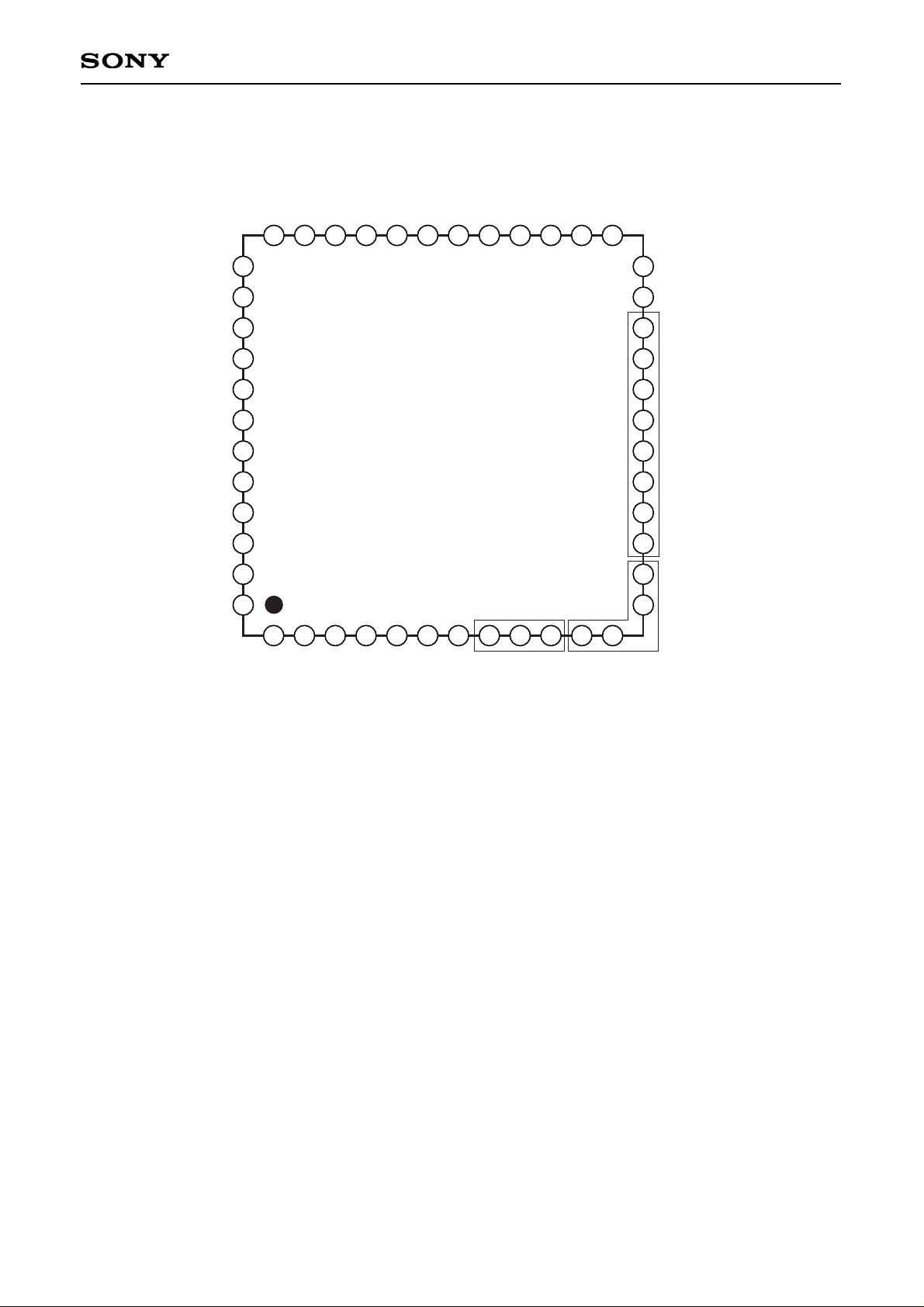
Pin Configuration (Top View)
1 2 3 4 5 6 7 8 9 10 11 12
13
14
15
16
17
18
19
20
21
22
23
24
2526272829
30
313233343536
37
38
39
40
41
42
43
44
45
46
47
48
The enclosed pins use separate power supplies.
H2
AVD1
XCPDM
AVD2
XSHP
XSHD
XRS
V
SS3
PBLK
XCPOB
ADCLK
RST
MCK
VDD1
2MCK
TEST2
SEN
SSK
SSI
ID
EXP
HRO
FRO
V
SS4
H1
V
SS2
V
SS1
RG
AVD0
TEST1
V
DD0
OSCI
OSCO
CKI
V
SS0
CKO
PS
DSGAT
VL
SUB
V2B
VH
V2A
V3
V1
VM
FRI
HRI
Page 4
– 4 –
CXD2457R
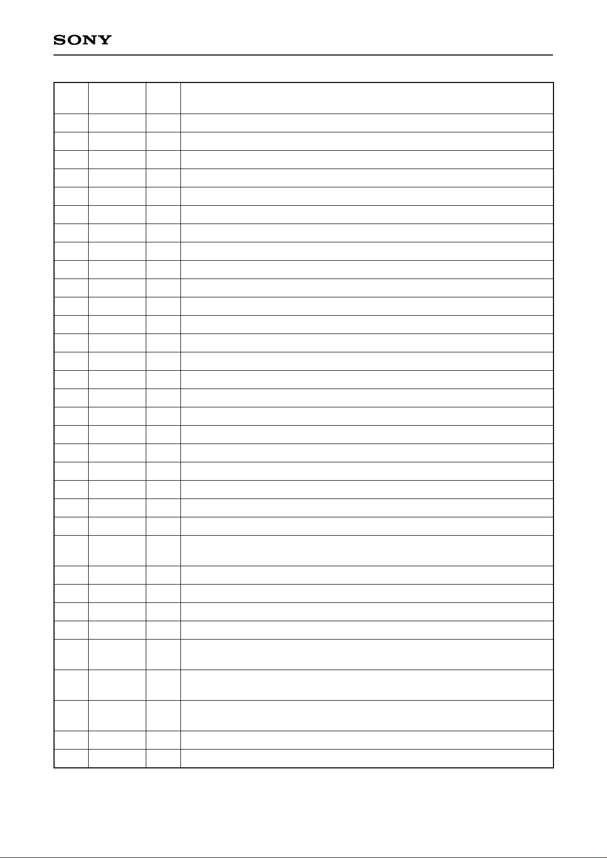
Pin Description
Pin
No.
1
2
3
4
5
6
7
8
9
10
11
12
13
14
15
16
17
18
19
20
21
22
23
24
25
26
27
28
29
30
31
32
33
CKO
Vss0
CKI
OSCO
OSCI
VDD0
TEST1
AVD0
RG
Vss1
Vss2
H1
H2
AVD1
XCPDM
AVD2
XSHP
XSHD
XRS
VSS3
PBLK
XCPOB
ADCLK
RST
MCK
VDD1
2MCK
TEST2
SEN
SSK
SSI
ID
EXP
O
—
I
O
I
—
I
—
O
—
—
O
O
—
O
—
O
O
O
—
O
O
O
I
O
—
O
I
I
I
I
O
O
Oscillator output. (30.0MHz)
GND
Oscillator input. (30.0MHz)
Inverter output for oscillation. (30.0MHz)
Inverter input for oscillation. (30.0MHz)
Power supply.
Test. With pull-down resistor. Fix to low.
Power supply.
Reset gate pulse output.
GND
GND
Clock output for horizontal CCD drive.
Clock output for horizontal CCD drive.
Power supply.
Clamp pulse.
Power supply.
Sample-and-hold pulse.
Sample-and-hold pulse.
Sample-and-hold pulse.
GND
Blanking cleaning pulse.
Clamp pulse.
Clock output for AD conversion.
Reset (Low: Reset, High: Normal operation).
Always input one reset pulse during power-on.
Clock output for digital circuit.
Power supply.
Clock output for digital circuit.
Test. Fix to high.
PS = High: Drive frequency setting input.
PS = Low: Serial setting strobe input.
PS = High: Readout method setting input.
PS = Low: Serial setting clock input.
PS = High: Shutter speed setting input.
PS = Low: Serial setting data input.
Line identification signal output write enable pulse output or XSUB output.
Pulse output indicating exposure is underway or checksum result output.
Symbol I/O Description
Page 5
– 5 –
CXD2457R
Pin
No.
34
35
36
37
38
39
40
41
42
43
44
45
46
47
48
HRO
FRO
VSS4
HRI
FRI
VM
V1
V3
V2A
VH
V2B
SUB
VL
DSGAT
PS
O
O
—
I
I
—
O
O
O
—
O
O
—
I
I
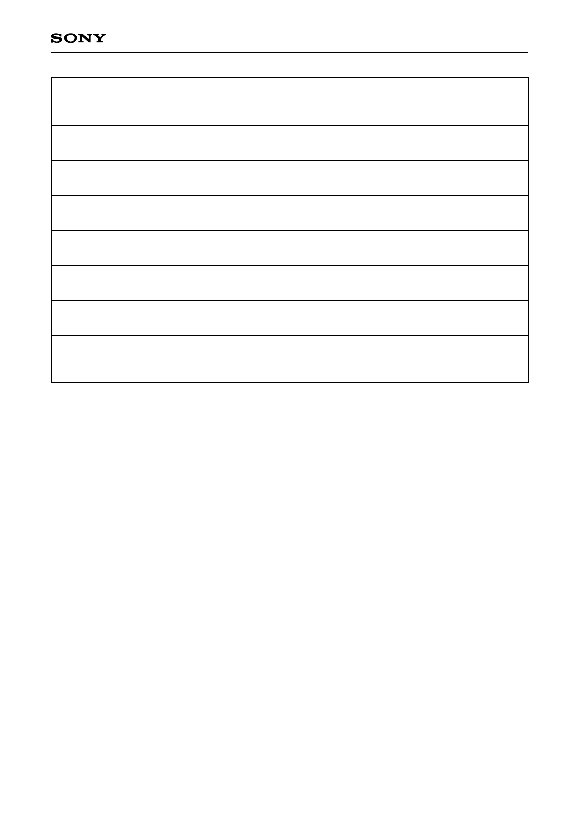
Horizontal sync signal (HR) output or XSGB output.
Vertical sync signal (FR) output or XSGA output.
GND
Horizontal sync signal (HR) input.
Vertical sync signal (FR) input.
GND (vertical clock driver GND).
Clock output for vertical CCD drive.
Clock output for vertical CCD drive.
Clock output for vertical CCD drive.
15V power supply (vertical clock driver power supply).
Clock output for vertical CCD drive.
CCD electric charge sweep pulse output.
–7.5V power supply (vertical clock driver power supply).
Output stop (Same operation control as SLP when low).
Parallel/serial switching for mode setting input method.
(High: Parallel, Low: Serial) With pull-down resistor.
Symbol I/O Description
Page 6
– 6 –
CXD2457R
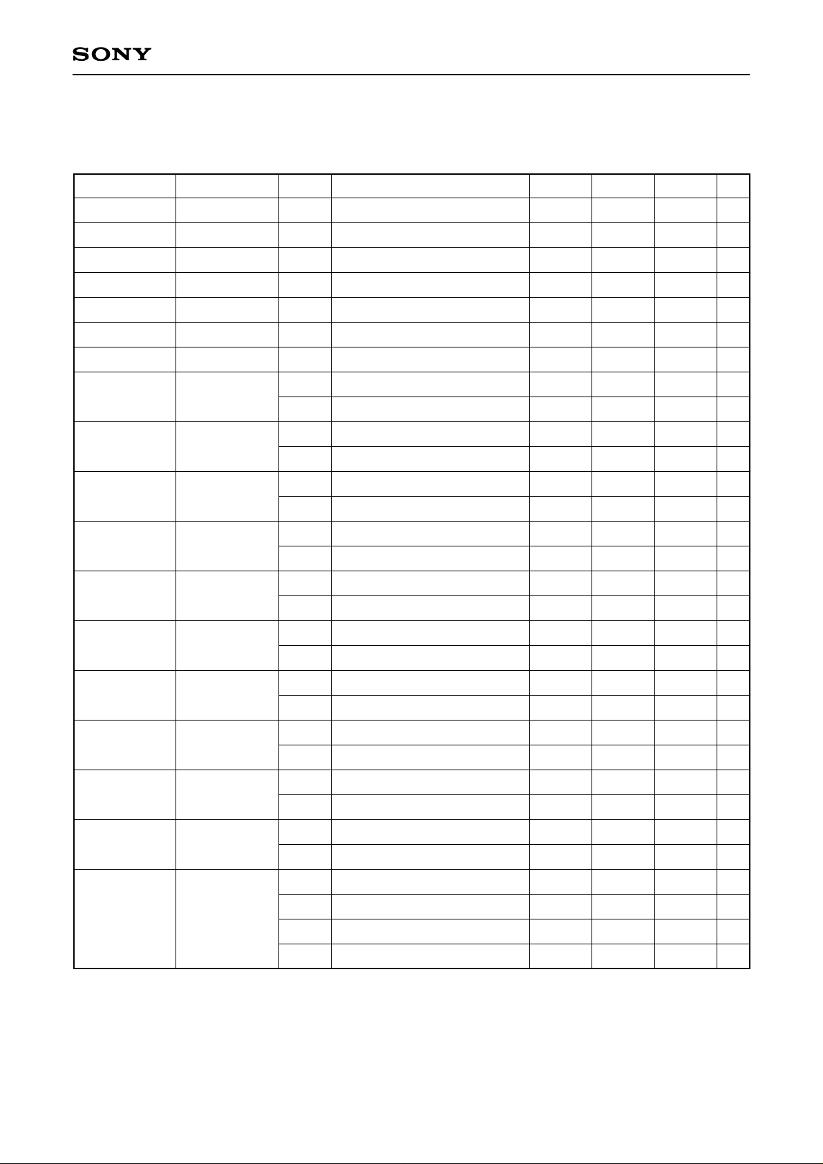
Electrical Characteristics
DC Characteristics
(Within the recommended operating conditions)
Item
Supply voltage 1
Supply voltage 2
Supply voltage 3
Supply voltage 4
Supply voltage 5
Supply voltage 6
Supply voltage 7
Input voltage 1
Input voltage 2
Input voltage 3
Output voltage 1
Output voltage 2
Output voltage 3
Output voltage 4
Output voltage 5
Output voltage 6
Output voltage 7
Output voltage 8
VDD0, VDD1,
AVD0
AVD1
AVD2
VH
VM
VL
CKI
TEST1, PS
RST, TEST2,
SEN, SSK, SSI,
HRI, FRI, DSGAT
CKO, MCK,
2MCK
RG
H1, H2
XCPDM, XSHP,
XSHD, XRS,
PBLK, XCPOB
ID, EXP, HRO,
FRO
SUB
V1, V3
V2A, V2B
VDDa
VDDb
VDDc
VDDd
VH
VM
VL
VIH1
VIL1
VIH2
VIL2
Vt + 1
Vt – 1
VOH1
VOL1
VOH2
VOL2
VOH3
VOL3
VOH4
VOL4
VOH5
VOL5
VOH6
VOL6
VOM7
VOL7
VOM101
VOM102
VOL8
VOL8
3.0
3.0
3.0
3.0
14.5
—
–9.0
0.7VDDa
0.7VDDb
0.8VDDa
VDDa – 0.8
VDDb – 0.8
VDDc – 0.8
VDDd – 0.8
VDDa – 0.8
VH– 0.25
VM– 0.25
VH– 0.25
VM– 0.25
3.3
3.3
3.3
3.3
15.5
0.0
3.6
3.6
3.6
3.6
15.5
—
–5.0
0.3VDDa
0.3VDDa
0.2VDDa
0.4
0.4
0.4
0.4
0.4
VL + 0.25
VL + 0.25
VM + 0.25
VL + 0.25
V
V
V
V
V
V
V
V
V
V
V
V
V
V
V
V
V
V
V
V
V
V
V
V
V
V
V
V
V
V
V
Feed current where IOH = –10.0mA
Pull-in current where IOL = 7.2mA
Feed current where IOH = –3.3mA
Pull-in current where IOL = 2.4mA
Feed current where IOH = –22.0mA
Pull-in current where IOL = 14.4mA
Feed current where IOH = –3.3mA
Pull-in current where IOL = 2.4mA
Feed current where IOH = –2.4mA
Pull-in current where IOL = 4.8mA
Feed current where IOH = –4.0mA
Pull-in current where IOL = 5.4mA
Feed current where IOH = –5.0mA
Pull-in current where IOL = 10.0mA
Feed current where IOH = –7.2mA
Pull-in current where IOL = 5.0mA
Feed current where IOH = –5.0mA
Pull-in current where IOL = 10.0mA
Pins Symbol Conditions Min. Typ. Max. Unit
Page 7

– 7 –
CXD2457R
Inverter I/O Characteristics for Oscillation
(Within the recommended operating conditions)
Item
Logical Vth
Input voltage
Output voltage
Feedback resistor
Oscillator frequency
OSCI
OSCI
OSCO
OSCI, OSCO
OSCI, OSCO
LVth
VIH
VIL
VOH
VOL
RFB
f
0.7VDDd
VDDa/2
500k
20
VDDa/2
2M
0.3VDDa
VDDa/2
5M
50
V
V
V
V
V
Ω
MHz
Feed current where IOH = –6.0mA
Pull-in current where IOL = 6.0mA
VIN = VDDd or Vss
Pins
Symbol
Conditions Min. Typ. Max. Unit
Base Oscillation Clock Input Characteristics (Within the recommended operating conditions)
Item
Logical Vth
Input voltage
Input amplification
CKI
LVth
VIH
VIL
VIN
0.7VDDa
0.3
VDDa/2
0.3VDDa
V
V
V
Vp-p
fmax 50MHz sine wave
Pins
Symbol
Conditions Min. Typ. Max.
Unit
∗1
Input voltage is the input voltage characteristics for direct input from an external source. Input amplification
is the input amplification characteristics for input through capacitor.
Switching Characteristics (VH = 15.0V, VM = GND, VL = –8.5V)
Item
Rise time
TTLM
TTMH
TTLH
350
450
50
250
300
50
550
700
80
400
450
80
1.0
1.0
1.0
1.0
ns
ns
ns
VL to VM
VM to VH
VL to VH
Fall time
TTML
TTHM
TTHL
ns
ns
ns
VM to VL
VH to VM
VH to VL
Output noise
voltage
VCLH
VCLL
VCMH
VCML
V
V
V
V
Symbol Conditions Min. Typ. Max.
Unit
∗1
The MOS structure of this IC has a low tolerance for static electricity, so full care should be given for
measures to prevent electrostatic discharge.
∗2
For noise and latch-up countermeasures, be sure to connect a bypass capacitor (0.1µF or more) between
each power supply pin (VH, VL) and GND.
Page 8

– 8 –
CXD2457R
Switching Waveforms
VH
VM
VL
TTMH
90%
10%
90%
10%
VM
VL
VH
VL
TTLH
90%
10%
TTLM
90%
10%
TTML
90%
10%
V2A (V2B)
TTLM
90%
10%
TTML
90%
10%
V1 (V3)
VSUB
TTHM
90%
10%
TTHL
Waveform Noise
VH
VL
VCLH
VCLL
VCMH
VCML
Measurement Circuit
R2
C1
C1
C2C2
C2C2
C1C1
R1
R1
R1
R1
V1
R1: 27Ω
R2: 5Ω
C1: 1500pF
C2: 3300pF
V3
V2A
V2B
Page 9

– 9 –
CXD2457R
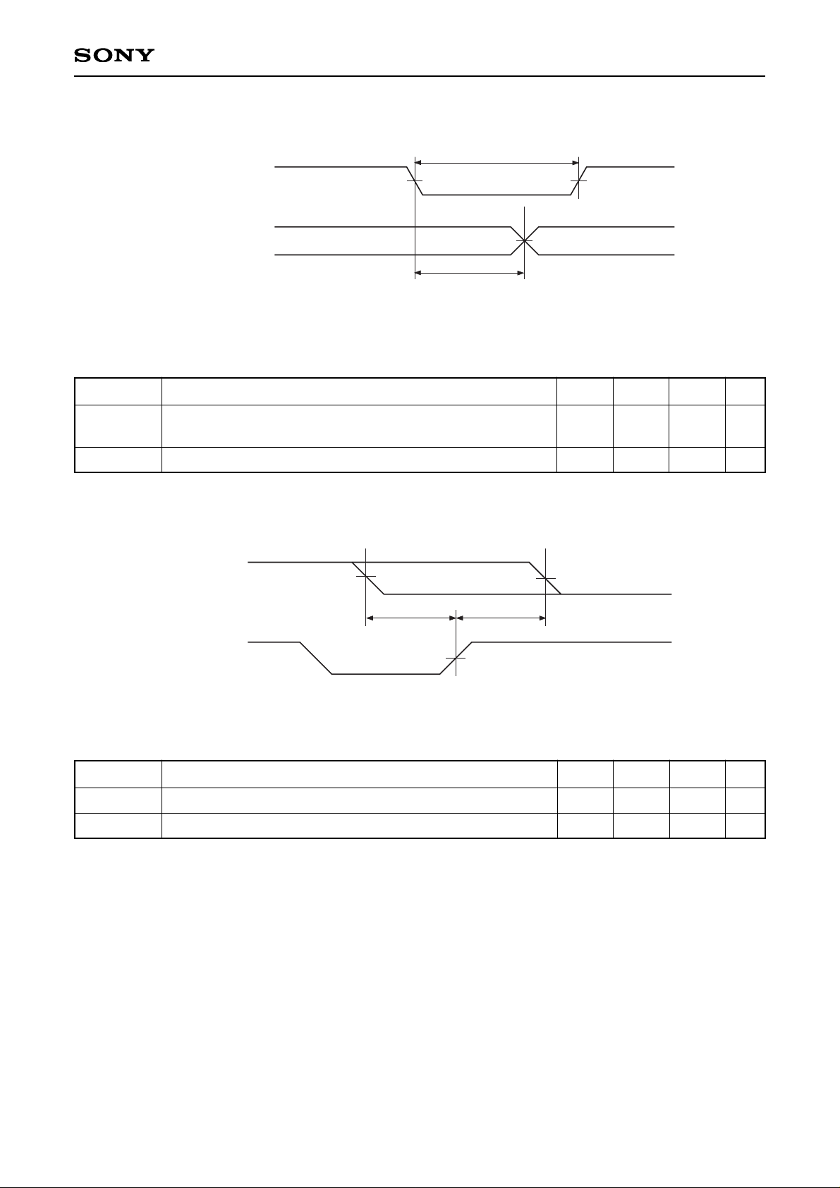
2) Serial interface clock internal loading characteristics
V2A
HRI
300ns
0.5V
DDa
0.5V
DDa
300ns
Do not rise the SEN level in this time
(300ns after the fall of HRI just before XSGA pulse generation
to 300ns after the fall of HRI just after XSGA pulse generation)
(Within the recommended operating conditions)
AC Characteristics
1) AC characteristics between the serial interface clocks
SSI
SSK
SEN
SEN
ts2
0.8V
DDa
0.8VDDa
0.2V
DDa
0.8V
DDa
0.2V
DDa
0.2V
DDa
th2
ts1
th1
ts3
Symbol
ts1
th1
ts2
th2
ts3
fk
SSI setup time, activated by the rising edge of SSK
SSI hold time, activated by the rising edge of SSK
SSK setup time, activated by the rising edge of SEN
SSK hold time, activated by the rising edge of SEN
SEN setup time, activated by the rising edge of SSK
SSK frequency
20
20
20
20
20
7.5
ns
ns
ns
ns
ns
MHZ
Definition Min. Typ. Max. Unit
Page 10
– 10 –
CXD2457R
4) FRI and HRI loading characteristics
tsSYNC thSYNC
0.5VDDa
0.5VDDa
0.5V
DDa
FRI, HRI
MCK
MCK load capacitance = 10pF (Within the recommended operating conditions)
Symbol
tsSYNC
thSYNC
FRI and HRI setup time, activated by the rising edge of MCK
FRI and HRI hold time, activated by the rising edge of MCK
5
5
ns
ns
Definition Min. Typ. Max. Unit
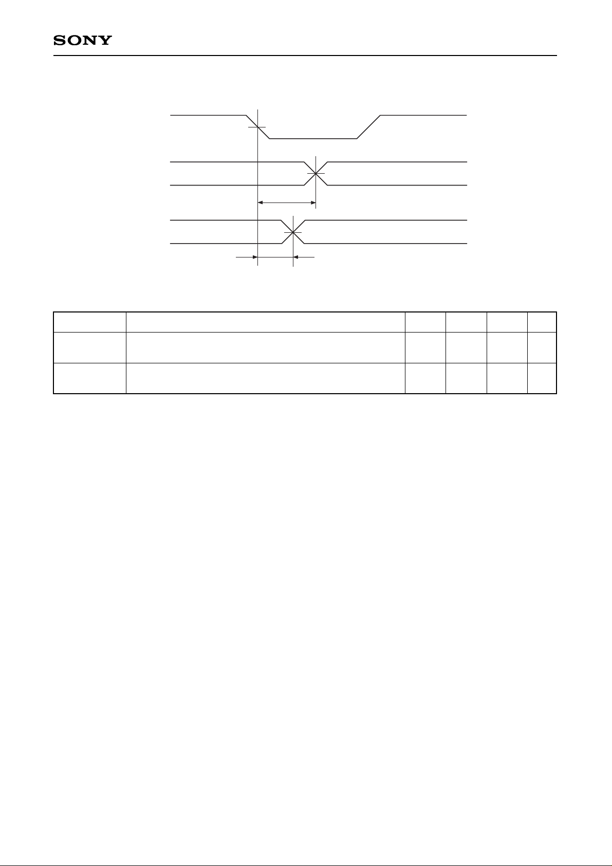
3) Output timing characteristics using DSGAT and RST
DSGAT, RST
EXP, XCPDM, XCPOB
PBLK, XSHP, XSHD, XRS,
RG, H1, H2
tpRST
twRST
0.5V
DDa
0.5VDDa
0.5VDDa, b, c, d
H1 and H2 load capacitance = 180pF
EXP, XCPDM, PBLK, XSHP, XSHD, XRS and RG load capacitance = 10pF
(Within the recommended operating conditions)
Symbol
tpRST
twRST
Time until the above outputs reach the specified value after
the fall of DSGAT and RST
RST and DSGAT pulse width
10
75 ns
ns
Definition
Min. Typ.
Max. Unit
Page 11
– 11 –
CXD2457R
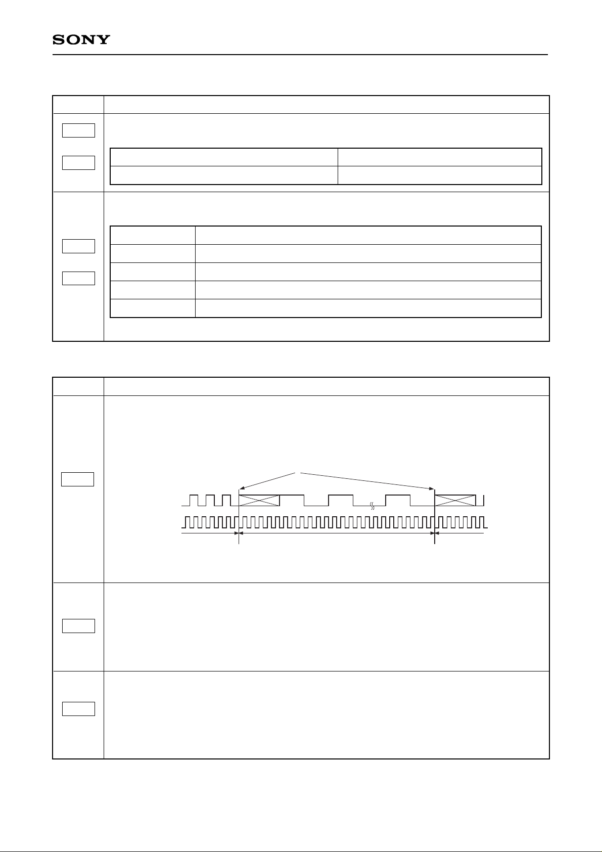
5) Output variation characteristics of ID, WEN, EXP, FRO and HRO
tpdEXP
tpdSYNCO
0.5V
DDa
0.5VDDa
0.5V
DDaMCK
EXP, ID, WEN
FRO, HRO
EXP, ID and WEN load capacitance = 10pF (Within the recommended operating conditions)
Symbol
tpdEXP
tpdSYNCO
Time until the WEN, ID and EXP outputs change after the
fall of MCK
Time until the FRO and HRO outputs change after the fall
of MCK
0.5
1.0
8.5
11.5nsns
Definition Min. Typ. Max. Unit
Page 12

– 12 –
CXD2457R
Data
D00
to
D07
CHIP
Chip switching
See D00 to D07
CHIP.
All 0
D08
to
D10
CTGRY
Category switching
See D08 to D10
CTGRY.
All 0
D11
to
D31
DATA
Control data for each category
The meaning of this CTGRY control data
differs according to the category set by D08 to
D10.
See D11 to D31
DATA.
All 0
D32
to
D39
Checksum bits
Checksum bits
See D32 to D39
CHKSUM.
All 0
Symbol
Function
When reset
Description of Operation
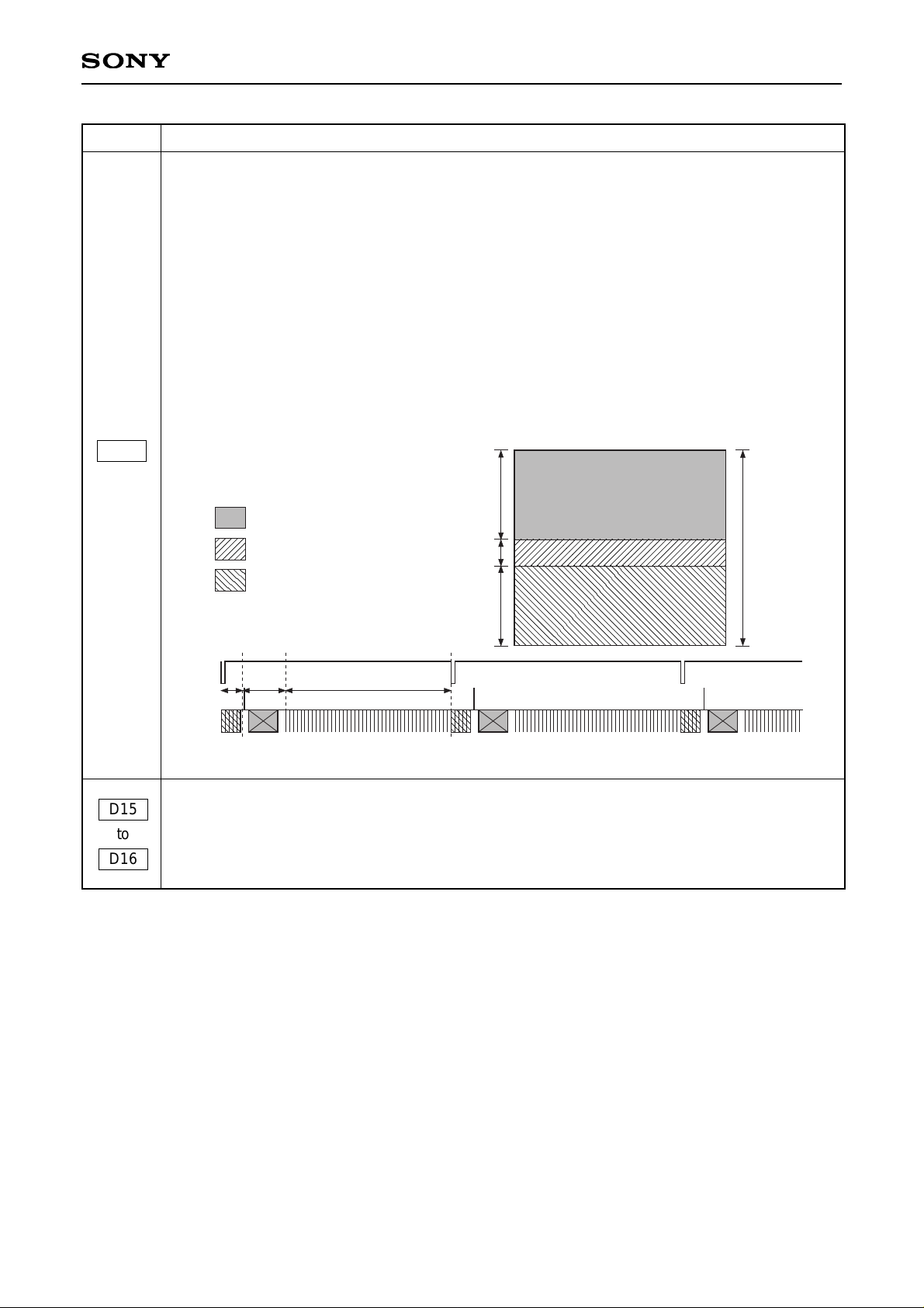
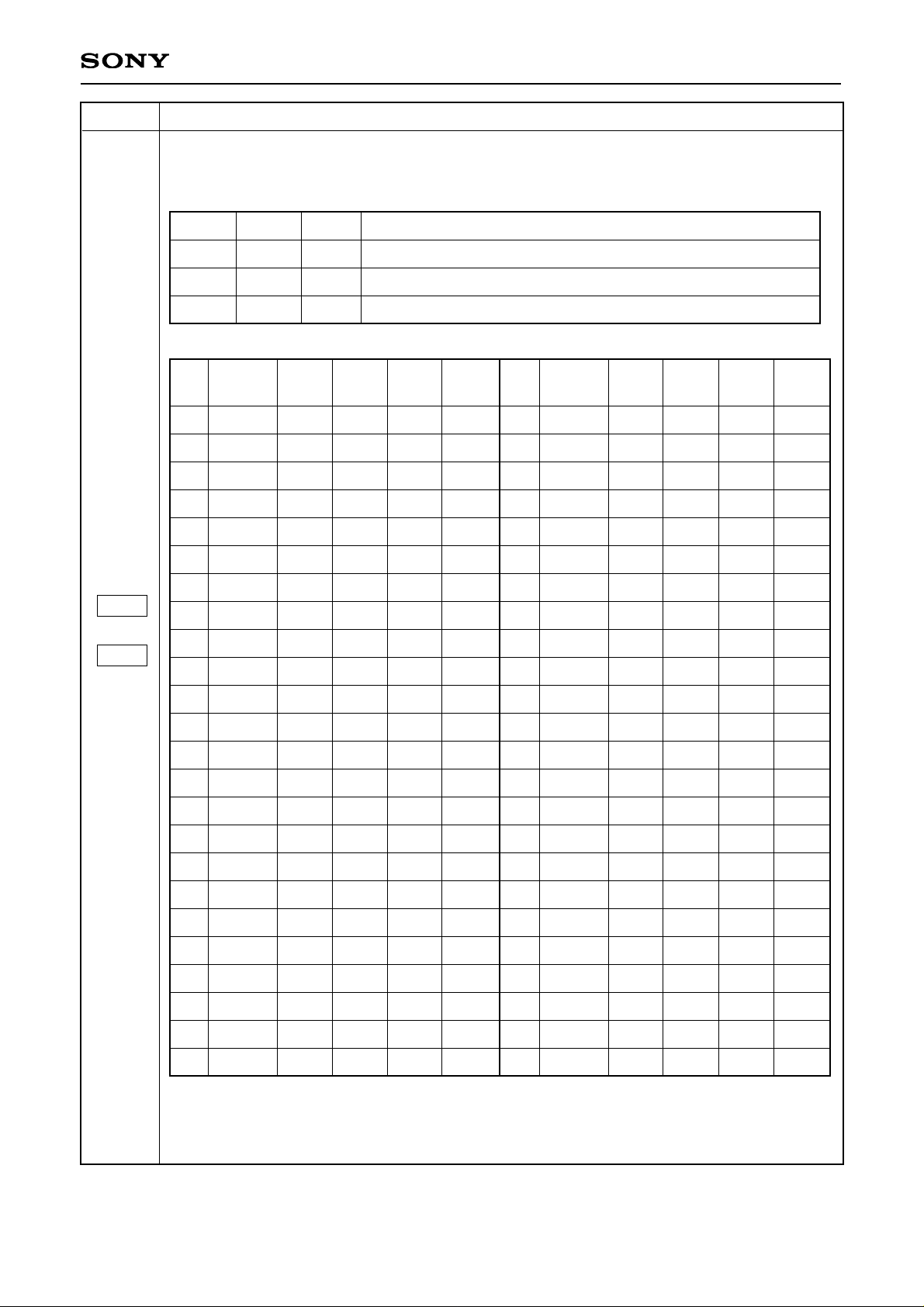
1. Progressive Scan CCD drive pulse generation
• Combining this IC with a crystal oscillator generates a fundamental frequency of 30.0MHz.
• CCD drive pulse generation is synchronized with HRI and FRI.
• The CCD drive method can be changed to various modes by inputting serial data or parallel data to the
CXD2457R.
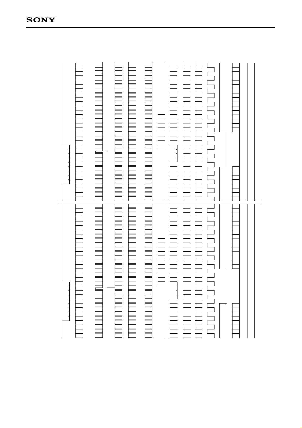
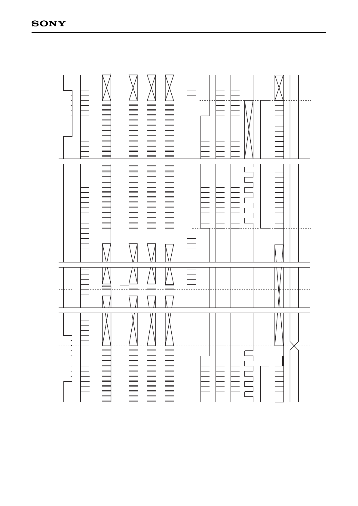
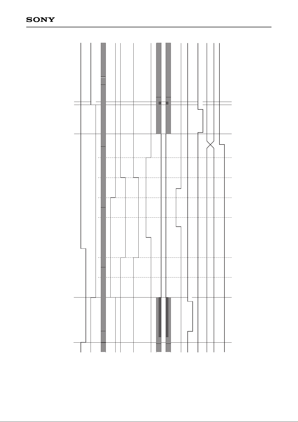
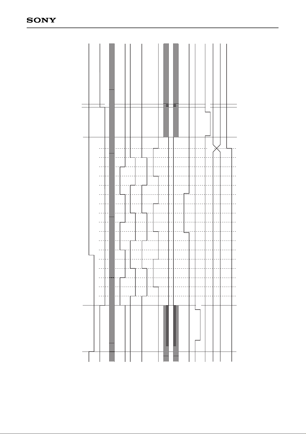
• The various drive methods possessed by the CXD2457R are shown in the Timing Charts A-1 to 4 (V rate)
and B-1 to 6 (H rate).
2. Serial data input method
• All CXD2457R operations can be controlled via the serial interface. The serial data format is as follows.
00SSI
SSK
SEN
01 02 03 04 05 06 33 34 35 36 37 38 39
Serial data format
Serial data
Page 13
– 13 –
CXD2457R
D00
to
D07
CHIP
3. Serial data and description of functions
Detailed description
The serial interface data is loaded to the CXD2457R when D00 and D07 are 1. However, this
assumes that D32 to D39 CHKSUM is satisfied.
D07 D06 D05 D04 D03 D02 D01 D00
1 0 0 0 0 0 0 1
Function
Loading to the CXD2457R
D08
to
D10
CTGRY
This CTGRY data indicates the functions that the serial interface data controls.
D10 D09 D08
0 0 0
0 1 0
0 1 1
1 0 0
Function
Mode control data
Electronic shutter control data
High-speed phase adjustment data (Set all of D11 to D31 to 0.)
System setting data
Input of values other than those listed above is prohibited.
D11
FHIGH
CTGRY: Mode control data
Detailed description
0: Power saving drive mode
1: High-speed drive mode
When FHIGH = 0, the clock input to CKI is immediately frequency divided by 1/3 and loaded
internally.
The high-speed phases of H1, H2, RG, XSHP, XSHD, XRS, ADCLK and other pulses are always
logically the same phase with respect to MCK.
0: DRAFT mode
1: FINE mode
In FINE mode, image data is taken by the normal Progressive Scan method.
In DRAFT mode, image data is taken by pulse elimination readout. This enables a frame rate
three times that during FINE mode. The mode is switched at the fall of HRI just before XSGA.
Note that the FRO output is also switched accordingly. (DRAFT mode: 264H, FINE mode: 792H)
0: Normal operation
1: Readout prohibited mode
In readout prohibited mode, a readout pulse is not added to V2A and V2B (V2A or V2B takes a
VH value). (V1, V2 and V3 are not modulated.)
The mode is normally switched at the fall of HRI just before the position where the readout pulse
is added.
D12
FINE
D13
NSG
MCK
CKI
Mode switching timing
(5 clocks after the fall of HRI just before XSG is generated)
Unstable
FHIGH = 1 FHIGH = 0 FHIGH = 1
Unstable
Page 14
– 14 –
CXD2457R
D14
FS
Detailed description
0: Normal operation
1: FS mode
In order to increase the frame rate, a certain portion of the captured image of CCD can be cut out
by performing high-speed sweep.
In FS mode, high-speed sweep is performed for the V registers of the entire image (period Z)
after FRI input. Next, high-speed sweep is performed again for only the desired period (period X)
after generating the XSGA pulse. Then, after performing normal V transfer and outputting the
effective signal (period Y), high-speed sweep is performed for the entire image again by inputting
FRI at the desired timing. This makes it possible to take only the desired portion in the V
direction, thus effectively increasing the frame rate.
Operation is fixed during period Z, with 22 lines swept every 1H and repeating over a 36H period.
During period X, first XSGA is generated, then sweep operation starts. This period is set in serial
data FVFS (system setting data: D21 to D26) in HRI units.
Be sure to set FINE = 0 in this mode.
Set to 0.
,
,
,
,
,
,
,
D15
to
D16
• When the frame rate is increased as the
vertical effective signal Y line (example)
Sweep variable period (period X)
X
Timing chart
FRI
V2A
Effective signal period (period Y)
Sweep fixed period (period Z)
Z X
Set by FVFS
36H
(Fix)
Reset by FRI after
normal transfer
Y
Y
1068
Z
,
Page 15
– 15 –
CXD2457R
Detailed description
Operation control settings
The operating mode control bits are loaded to the CXD2457R at the rise timing of the SEN input,
and control is applied immediately.
D17
to
D18
STB
D18 D17 Symbol Control mode
0 0 CAM Normal operation mode
0 1 SLP
Sleep mode (mode for the status where CCD drive is not required)
1 X STN Standby mode
Pin
No.
Symbol
CAM SLP
STN
RST
∗
Pin
No.
Symbol
CAM SLP
STN
RST
∗
1
CKO
ACT ACT
ACT ACT
25
MCK
ACT
ACT
ACT ACT
2
VSS0
— —
— —
26
VDD1
—
—
— —
3
CKI
ACT ACT
ACT ACT
27
2MCK
ACT
ACT
ACT ACT
4
OSCO
ACT ACT
ACT ACT
28
TEST2
—
—
— —
5
OSCI
ACT ACT
ACT ACT
29
SEN
ACT
ACT
— —
6
VDD0
—
—
—
—
—
—
—
—
—
—
—
—
30
SSK
ACT
ACT
— —
7
TEST1
31
SSI
ACT
ACT
— —
8
AVD0
32
ID
ACT
L
L L
9
RG
ACT L
L L
33
EXP
ACT
L
L L
10
VSS1
— —
— —
34
HRO
ACT
ACT
L L
11
VSS2
— —
— —
35
FRO
ACT
ACT
L L
12
H1
ACT L
L L
36
VSS4
—
—
— —
13
H2
ACT L
L L
37
HRI
ACT
ACT
— —
14
AVD1
— —
— —
38
FRI
ACT
ACT
— —
15
XCPDM
ACT L
L L
39
VM
—
—
— —
16
AVD2
— —
— —
40
V1
ACT
VM
VM VM
17
XSHP
ACT L
L L
L
L L
L
L L
41
V3
ACT
VM
VM VM
18
XSHD
ACT
42
V2A
ACT
VH
VH VH
19
XRS
ACT
43
VH
—
—
— —
20
VSS3
— —
— —
44
V2B
ACT
VH
VH VH
21
PBLK
ACT L
L L
L
L L
L
L L
45
SUB
ACT
VH
VH VH
22
XCPOB
ACT
46
VL
—
—
— —
23
ADCLK
ACT
47
DSGAT
ACT
ACT
L L
24
RST
ACT ACT
ACT ACT
48 PS
ACT
ACT
ACT ACT
Pin status during operation control
∗
See "6. RST pulse" for a detailed description of RST.
Note) ACT indicates circuit operation, and L indicates "low" output level in the controlled status.
For sleep mode or standby mode, stop supplying VH and VL power supplies with CCD
image sensor.
Page 16

– 16 –
CXD2457R
D19
EXPXEN
Detailed description
0: The EXP pulse indicating the exposure period is generated.
1: The EXP pulse indicating the exposure period is not generated, and is constantly fixed to low.
This bit is invalid when STATUS = 1.
Note that the STB setting has priority.
The data is reflected at the rise of XSGA.
Invalid data
Low-speed electronic shutter setting.
The value set here is the number of FR during which readout operation is not performed even if
there is input. The setting range is from 0 to 31. When set to 0, readout operation is performed at
the first VR.
When FS = 1, this bit is invalid.
D20
3MCK
0: 2MCK clock system
1: 3MCK clock system
This bit switches how MCK is comprised from the clock selected by FHIGH. Note that the
waveform is unstable for 5 clocks before and after switching.
D21
to
D23
Invalid data
D29
to
D31
D24
to
D28
VSHUT
MSB LSB
D28 D27 D26 D25 D24
Function
Number of FR during which readout operation is not performed
CXD2457R clock system
When using a 30MHz crystal
Mode1
Mode2
Mode3
Mode4
Mode5
1
1
0
1
1
FHIGH
0
1
0
0
1
3MCK
1
0
0
0
1
FINE
15MHz
10MHz
5MHz
15MHz
10MHz
30MHz
15MHz
10MHz
30MHz
15MHz
15Frame/s
30Frame/s
15Frame/s
45Frame/s
10Frame/s
MCK frequency
2MCK pin output
Frame rate
Note) Combinations of FHIGH, 3MCK and FINE other than those listed above are prohibited.
Page 17

– 17 –
CXD2457R
Detailed description
High-speed electronic shutter setting.
The value set here is the number of SUB pulses from FR to the next FR.
Input 0.
D21
to
D31
D11
to
D20
HSHUT
MSB LSB
D20 D19 D18 D17 D16 D15 D14 D13 D12 D11
Function
Number of SUB pulses setting
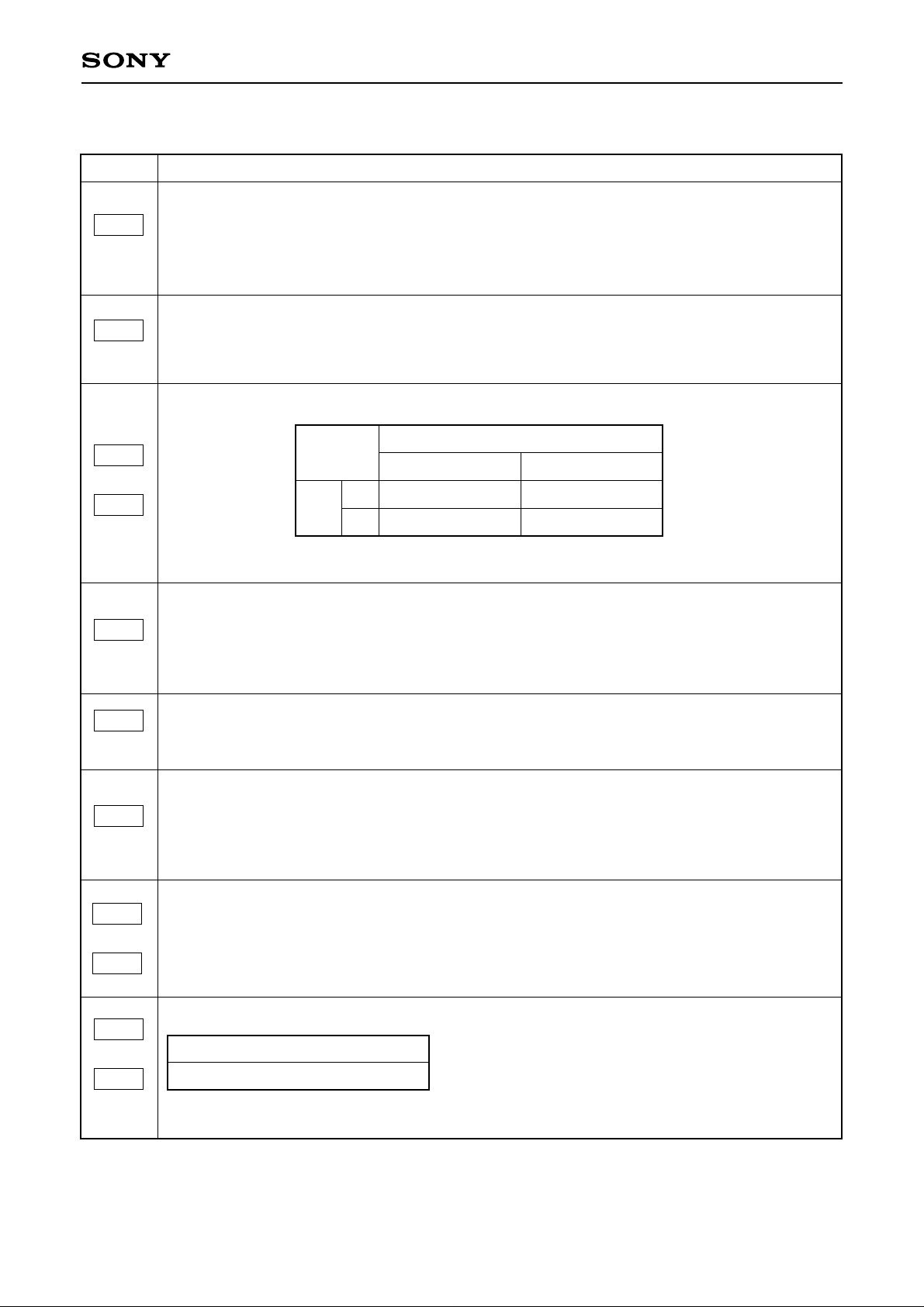
High-speed and low-speed electronic shutter can be used together. Therefore, the exposure time is as follows:
FR cycle × VSHUT + (fv – HSHUT) × HR cycle + 745/MCK frequency [Hz] = Exposure time [s]
(fv: Number of HR in 1FR)
CTGRY: Electronic shutter control data
Page 18
Detailed description
– 18 –
D13
to
D14
IDSEL
D21
to
D26
FVFS
D11
SGXEN
0: Normal operation
1: XSGA and XSGB are output from the FRO and HRO pins.
Note that the amplitude of the output pulses are VSS to VDDa.
These bits select the pulse output from the ID pin.
XSUB: Inverted SUB pulse output at the amplitude of VSS to VDDa
D12
EXSG
0: VT (readout clock) is added to V2A, V2B and V3 as normal.
1: VT is not added to V2A, V2B and V3.
During readout, only the modulation necessary for readout is performed.
Note that this setting has priority over mode control data NSG (D13).
D15
VTXEN
0: Checksum is not performed and the checksum data is invalid. (However, dummy data must be
set in the CHKSUM register.)
1: Checksum is performed. This data is reflected even if the checksum results are NG.
D16
CHKSUM
0: The EXP pulse is output from the EXP pin.
1: High is indicated if the checksum results are OK, and low if the results are NG.
This pulse is output at the rise of SEN, and reset high at the fall of SEN. This pulse has priority
over mode control data EXP.
D17
STATUS
D13
0
1
D14
0
ID pulse output
XSUB pulse output
1
WEN pulse output
ID pulse output
Input 0.
These bits set the high-speed sweep period (unit: H) in FS mode.
The high-speed sweep is performed 22 times every 1H.
D18
to
D20
MSB LSB
D26 D25 D24 D23 D22 D21
CXD2457R
CTGRY: System setting data
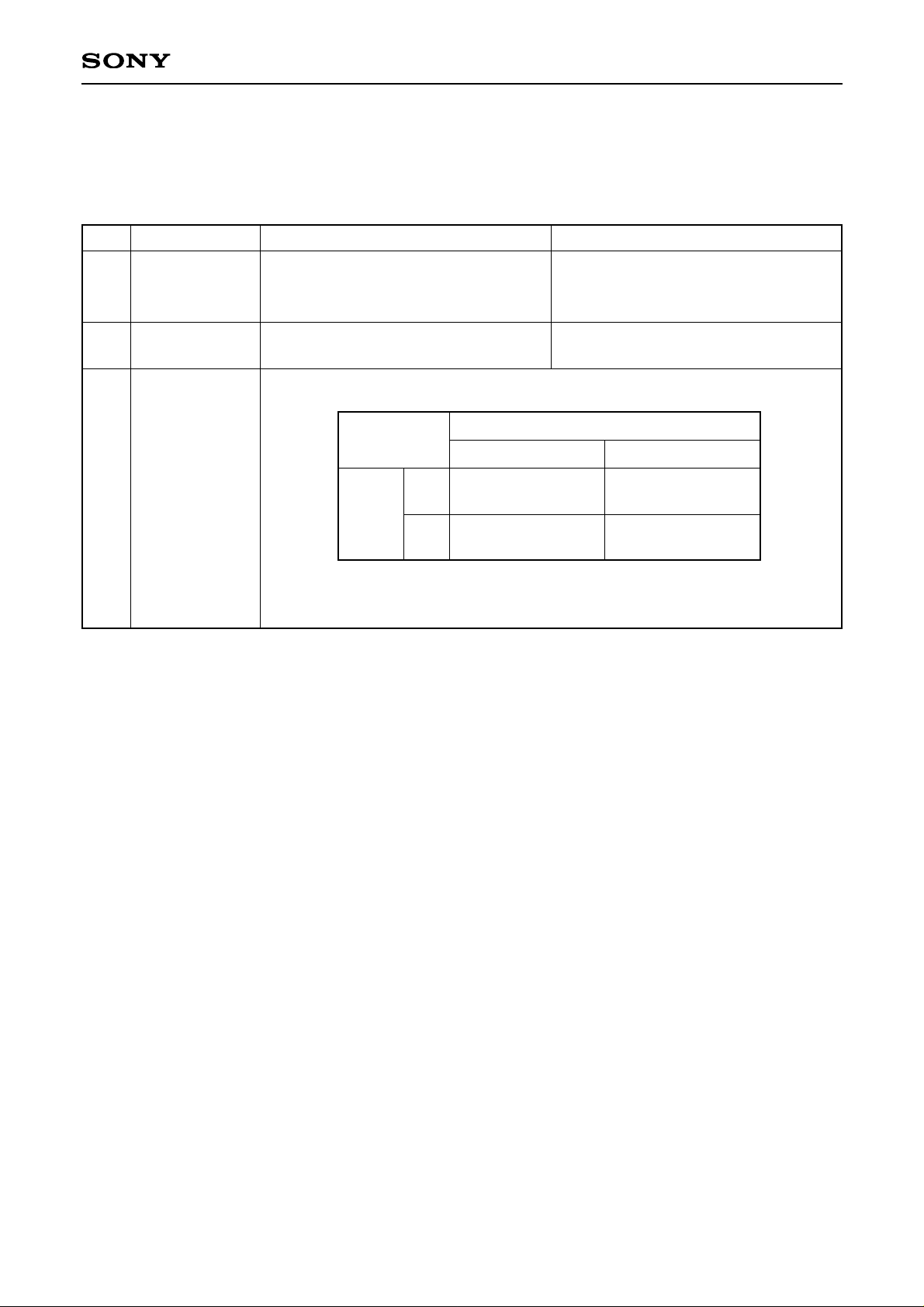
0: Internal SSG (Sync Signal Generator) functions operate to generate FRO and HRO.
1: Internal SSG functions are stopped, and the FRO and HRO pulses are fixed to low.
Note that the STB setting has priority. When the sync signal is input from external CXD2457R,
use it at SGXEN = 1.
Page 19

– 19 –
CXD2457R
Detailed description
0: Normal operation
1: V1, V2 and V3 are inverted and output as XV1, XV2 and XV3. The amplitude is from VL to VM.
D27
XVCK
Invalid data
D28
to
D31
Detailed description
D32
to
D39
These are the checksum bits.
MSB LSB
D07 D06 D05 D04 D03 D02 D01 D00
D15 D14 D13 D12 D11 D10 D09 D08
D23 D22 D21 D20 D19 D18 D17 D16
D31 D30 D29 D28 D27 D26 D25 D24
+) D39 D38 D37 D36 D35 D34 D33 D32 → CHKSUM
If the total = 0, the checksum results are OK.
Serial data is loaded to the internal registers only when checksum is OK.
Data is not reflected to the registers if checksum is NG.
Also, when CHKSUM = 0, the checksum results are always OK and the data is reflected to the
registers.
CHKSUM
Page 20
Serial register FINE = 1 and the
CXD2457R operates in FINE mode.
– 20 –
CXD2457R
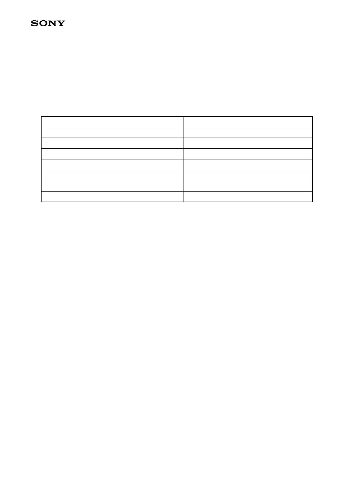
4. Shutter speed setting specifications when PS = H
When PS = H, the CXD2457R can be controlled without inputting serial data by using the SEN, SSK and SSI
pins.
Other registers hold the value input when PS = L, and assume the status indicated by STB when the RST
pulse is input.
Pin When H
SEN
When L
Serial registers FHIGH and 3MCK = 0.
Serial registers FHIGH = 1 and
3MCK = 0.
FHIGH
(horizontal CCD
drive frequency)
SSK
Serial register FINE = 0 and the
CXD2457R operates in DRAFT mode.
FINE
(readout method)
SSI
Number of SUB pulses when PS = H
HSHUT,
VSHUT
(exposure time)
SEN
L
H
SSK
L H
249
199
777
727
217
68
745
596
Upper number: When SSI = H (1/250)
Lower number: When SSI = L (1/60)
Page 21
– 21 –
CXD2457R
5. Reflective position of each data
Each serial data is reflected at the timing shown in the table below. The reflection position is the same when
PS = H. When using the low-speed electronic shutter, the data is not reflected at FR where XSGA is not
generated (a readout pulse is not added to V2A).
Data Reflection position
Mode control data (STB)
Mode control data (EXPXEN)
Mode control data (other than STB and EXPXEN)
Electronic shutter control data
High-speed phase adjustment data
System setting data (SGXEN)
System setting data (other than SGXEN)
SEN rise
XSGA pulse rise
HRI∗1fall just before XSGA pulse generation
HRI∗2fall just after XSGA pulse generation
HRI∗1fall just before XSGA pulse generation
SEN rise
HRI∗1fall just before XSGA pulse generation
6. RST pulse
Setting Pin 30 to low resets the system. The serial data values after reset are as shown in the "Serial data"
table.
Also, some internal circuits stop operating when RST = L. For a description of the pin status when RST = L,
see the "Pin status during operation control" table given in the detailed description of STB under "3. Serial data
and description of functions".
7. DSGAT
DSGAT is ON when low and the CXD2457R is set to sleep mode as with SLP of STB.
Note that control is applied when either or both of DSGAT and SLP are ON. Also, when STN is ON, the
CXD2457R is set to standby mode regardless of the DSGAT status.
8. EXP pulse
The EXP pulse indicates the exposure period.
The details are shown on the following pages.
Table 5-1. Serial data reflection timing
∗1
For FS mode, 7HRI later from FRI fall
∗2
For FS mode, 8HRI later from FRI fall
Page 22
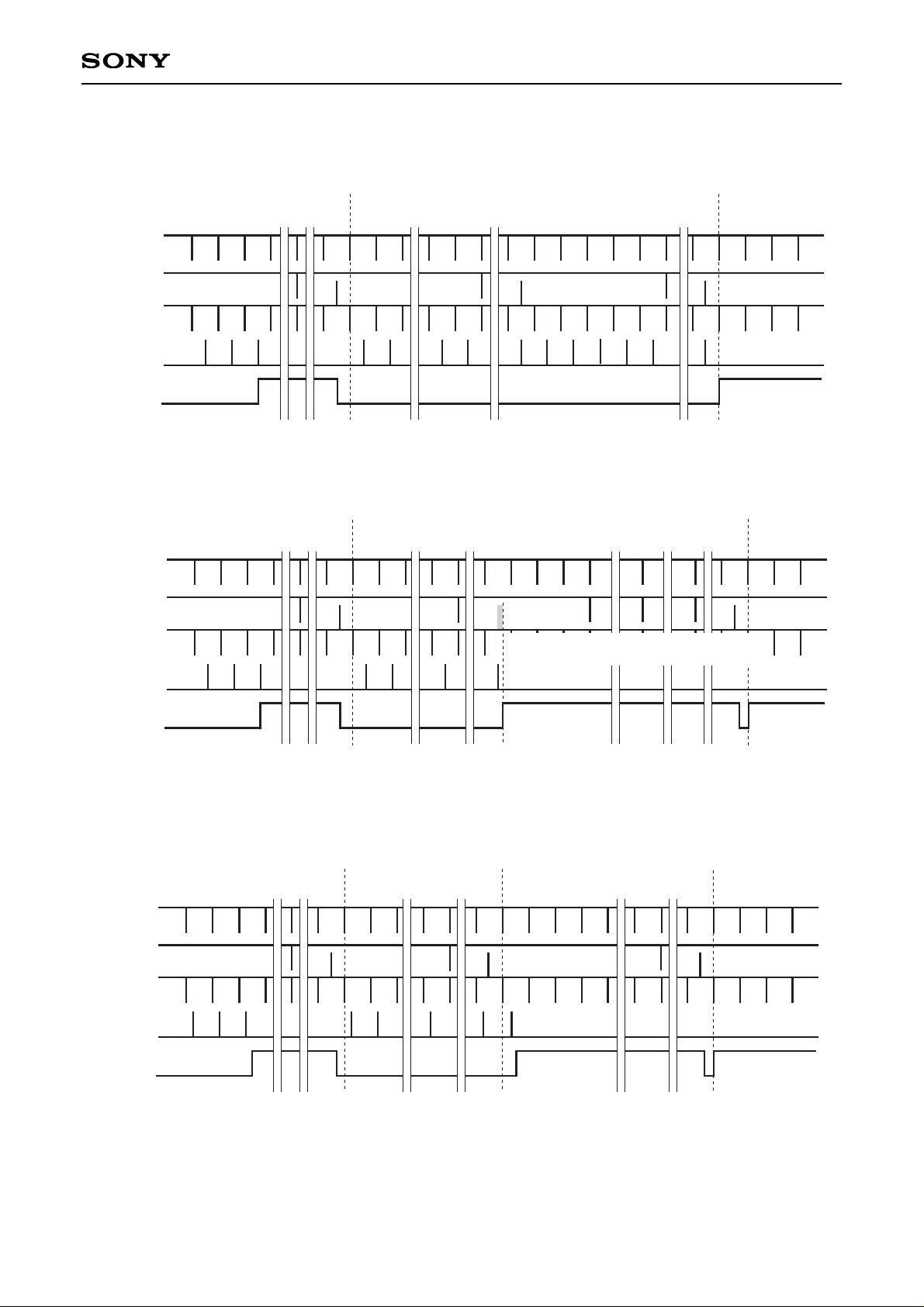
– 22 –
CXD2457R
HRI
MAX 1 to MAX
0 0 08 (42) 8 (42) 8 (42)
0
FRI
V2A
SUB
EXP
value of
HSHUT
(1) HSHUT ≥ MAX
HRI
MAX1 to MAX
0 0 08 (42) 8 (42) 8 (42)
0
FRI
V2A
SUB
EXP
Location where XSG is normally generated.
(However, this pulse is not actually generated.)
value of
HSHUT
(2)HSHUT ≥ MAX (with low-speed erectronic shutter)
HRI
MAX 1 to MAX1 to MAX
0 0 08 (42) 8 (42) 8 (42)
0
FRI
V2A
SUB
EXP
value of
HSHUT
(3) 1 ≤ HSHUT < MAX
Numbers in parentheses are for FS mode.
Page 23
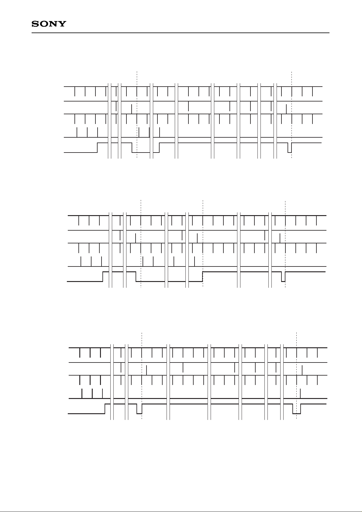
– 23 –
CXD2457R
HRI
1 to MAX (with low-speed erectronic shutter)1 to MAX
0 08 (42) 8 (42)
0
FRI
V2A
SUB
EXP
value of
HSHUT
(4) 1 ≤ HSHUT < MAX (with low-speed erectronic shutter)
HRI
MAX1 to MAX
0 0 08 (42) 8 (42) 8 (42)
00
FRI
V2A
SUB
EXP
value of
HSHUT
(5) HSHUT = 0
HRI
1 to MAX
0 08 (42) 8 (42)
FRI
V2A
SUB
EXP
value of
HSHUT
0 (with low-speed erectronic shutter)
(6) HSHUT = 0 (with low-speed erecyronic shutter)
Numbers in parentheses are for FS mode.
Page 24

– 24 –
CXD2457R
FRI
HRI
V2A
V2B
V3
SUB
PBLK
XCPOB
XCPDM
ID
WEN
OUT
Mode
V1
FINE mode
779 1 2 3 1779 2 34 5 6 7 1 2 3 4
792
1
8
9
1
792
790
788
(Chart B-3) (Chart B-1)
Chart A-1. FINE Mode (Vertical synchronization)
Page 25
– 25 –
CXD2457R
264
1
5
(Chart B-4) (Chart B-2)
10
15
20
262
264
1
5
10
15
20
HRI
V1
V2A
V2B
V3
SUB
PBLK
XCPOB
XCPDM
ID
WEN
OUT
Mode
DRAFT mode
757
760
763
766
769
772
251
252
253
254
255
256
7
10
13
16
19
22
1
2
3
4
5
6
25
28
31
7
8
9
7
10
13
16
19
22
1
2
3
4
5
6
25
28
31
7
8
9
757
760
763
251
252
253
766
769
772
254
255
256
FRI
Chart A-2. DRAFT Mode (Vertical synchronization)
Page 26
– 26 –
CXD2457R
FRI
HRI
V1
V2A
V2B
V3
SUB
PBLK
XCPOB
XCPDM
ID
WEN
OUT
Mode
DRAFT mode FS mode
The mode is switched at the point where XSG is normally generated.
The number of XSUB pulses is
specified by the serial data.
43
1
The number of sweeps is
specified by the serial data.
(Charts B-5/6) (Charts B-5/6) (Charts B-1/2)
1
7
8
9
The number of sweeps is fixed (792).
(Chart B-4)
Chart A-3. FS Mode (Vertical synchronization)
Page 27
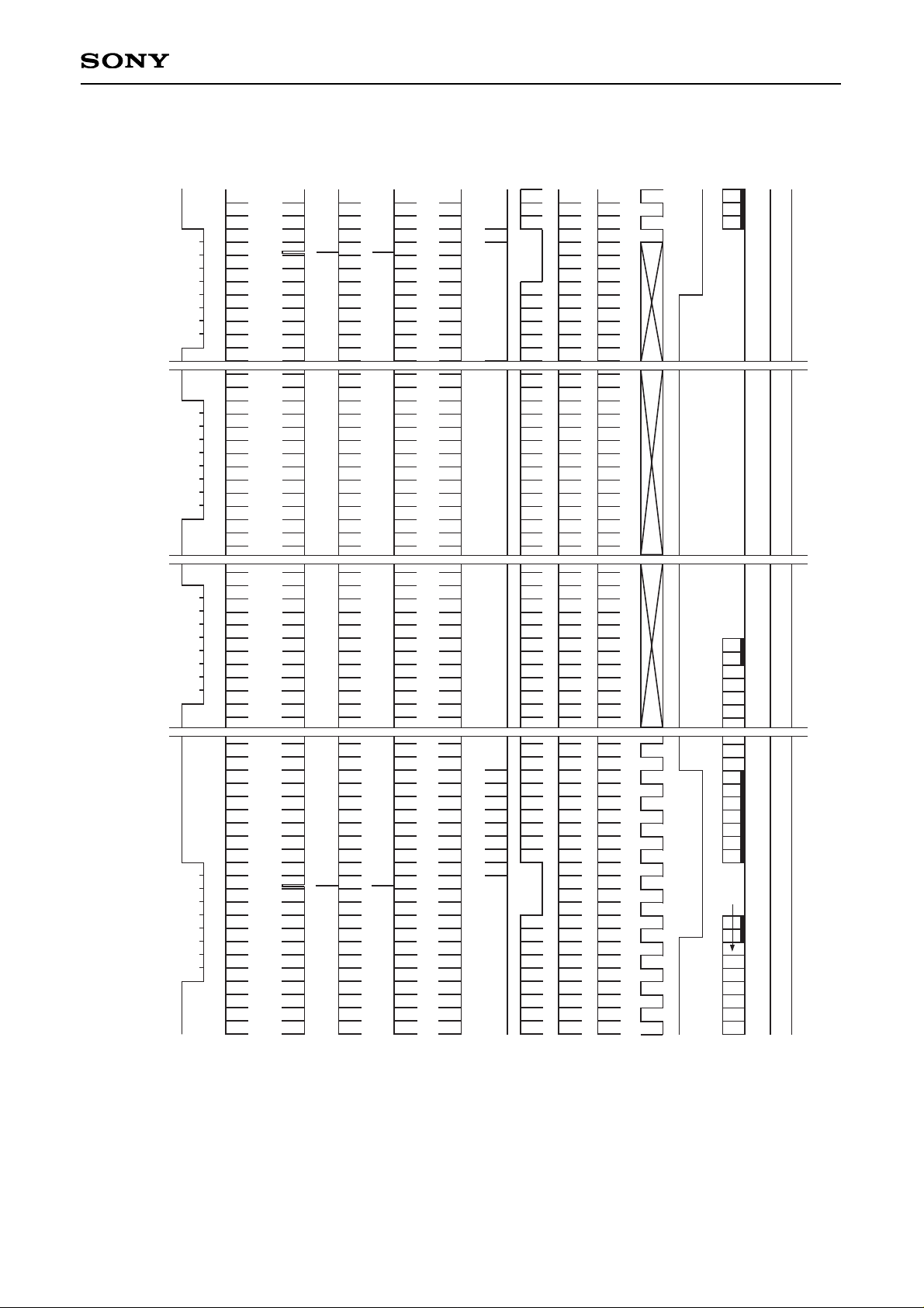
– 27 –
CXD2457R
FRI
HRI
V1
V2A
V2B
V3
SUB
PBLK
XCPOB
XCPDM
ID
WEN
OUT
779 1 2 3 1 2 34 5 6 7 1 2
Mode
FINE mode FINE mode FINE mode FINE mode
792
(Chart B-3) (Chart B-1)
1
8
9
1
Chart A-4. FINE Mode (Vertical synchronization) Low-speed electronic shutter
Page 28
– 28 –
CXD2457R
MCK
PBLK
HRI
9494
45
45
45
0/1270
0
0
V1
V2A
V2B
V3
H1
H2
SUB
XCPOB
XCPDM
ID/WEN
EXP
241
85
145
165
105
185
116
154
198
211
198
209
11 41
234
238
Chart B-1. FINE Mode (Horizontal synchronization)
Page 29
– 29 –
CXD2457R
MCK
PBLK
HRI
0/1270
0
45
94
45 72 99 126 153 180
54 81 108 135 162 189
54 81 108 135 162 189
63 90 117 144
116 154
171 198
V1
V2A
V2B
V3
H1
H2
SUB
XCPOB
XCPDM
ID/WEN
EXP
209
241
211
198
11
198
238
234
41
Chart B-2. DRAFT Mode (Horizontal synchronization)
Page 30
– 30 –
CXD2457R
HRI
0 94
45 145 245
85 165
105 185
51 bits
848 bits
51 bits
2 bits
XV1
V2A/V2B
XV3
XSGA
XSGB
V1
V2A/V2B
V3
EXP
850
900
899
848
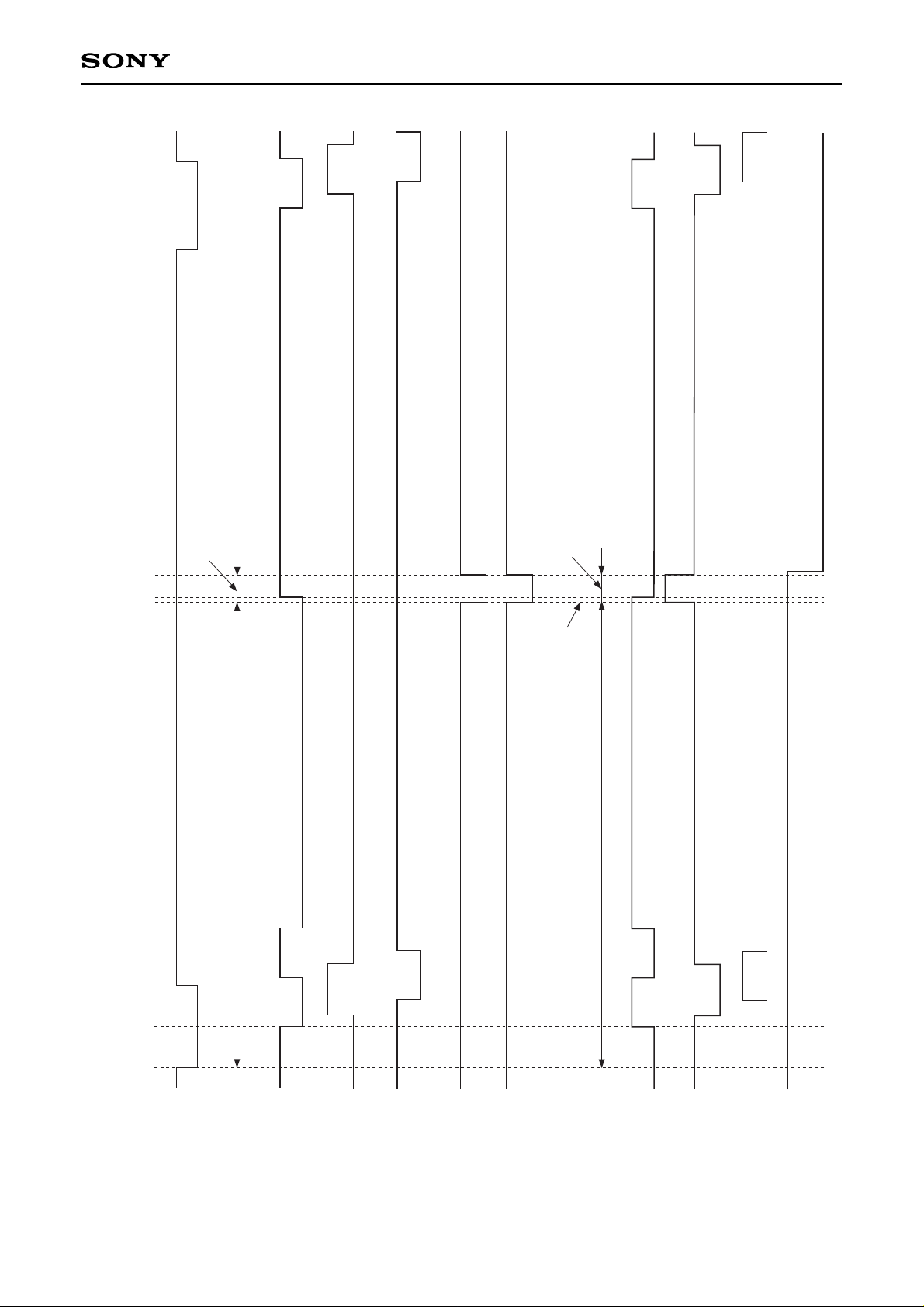
Chart B-3. Readout Timing (FINE mode)
Page 31

– 31 –
CXD2457R
HRI
0 94
848 bits
2 bits
54 bits
45 72 99 126 153 188
54 81 108 135 162 189
63 90 117 144 171 198
215
XV1
XV2A/B
XV3
XSGA
XSGB
V1
V2A
V2B
V3
EXP
9 99
9 99
848 899
100 bits
850 1001 1028
1046
1008 1037
1017
900
51 bits
Chart B-4. Readout Timing (DRAFT mode)
Page 32
– 32 –
CXD2457R
HRI
MCK
V1
V2A
V2B
V3
H1
H2
SUB
XCPOB
XCPDM
ID
WEN
EXP
PBLK
1
45
45
54
54
63 90 117 144 171
81 108 135 162
81 108 135 162
72 99 126 153
198
189
189
180
0
3 4 52
154
11
198
241
0/1270
94
116
209 238
234211
41
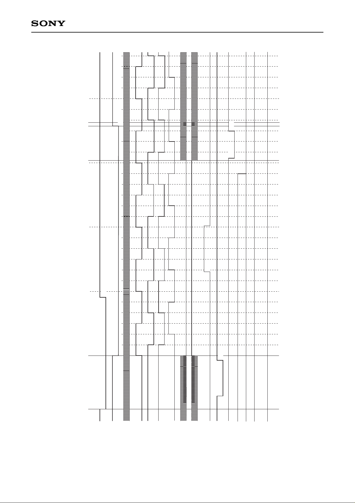
Chart B-5. FS Mode: V clock continuous drive start (Horizontal synchronization)
Page 33

– 33 –
CXD2457R
HRI
MCK
V1
V2A
V2B
V3
H1
H2
SUB
XCPOB
XCPDM
ID
WEN
EXP
PBLK
20 21 22
11
45
45 72
54 81
54 81
63
1233
0/1270
41
Chart B-6. FS Mode: V clock continuous drive end (Horizontal synchronization)
Page 34

– 34 –
CXD2457R
2MCK
MCK
H1
H2
RG
XSHP
XSHD
XRS
ADCLK
(3MCK = 0)
Logical Phase
Page 35
– 35 –
CXD2457R
XSHP
CDS/AGC
CXA2006Q
CCD Image
Sensor
ICX204AK
A/D
CXD2311AR
Signal Processor
Block
Controller
XSHD
XRS
2MCK
ADCLK
D0 to D9
MCK
ID
HRO
FRO
HRI
FRI
SEN
SSK
SSI
RST
EXP
V1
V2A
V2B
RG
CCDOUT
H1
H2
V3
SUB
XCPOB
DRVOUT
VRT
VRB
OSCO
CKI
OSCI
TEST1
TEST2
PS
+3.3V
XCPDM
PBLK
Timing Generator
CXD2457R
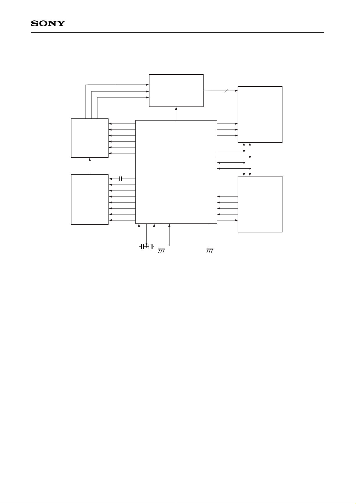
Application Circuit
For making FR and HR outside the CXD2457R, configure a circuit that counts MCK. (Using 2MCK, CKO, etc.
is not recommended.) Also, set system setting data, SGXEN (D11) to "1" and stop a built-in SSG.
Use crystal oscillator (fundamental wave) as base oscillation. Be sure to input duty 50% pulse when crystal
oscillator is used.
Application circuits shown are typical examples illustrating the operation of the devices. Sony cannot assume responsibility for
any problems arising out of the use of these circuits or for any infringement of third party patent and other right due to same.
Page 36
– 36 –
CXD2457R
Notes on Turning Power ON
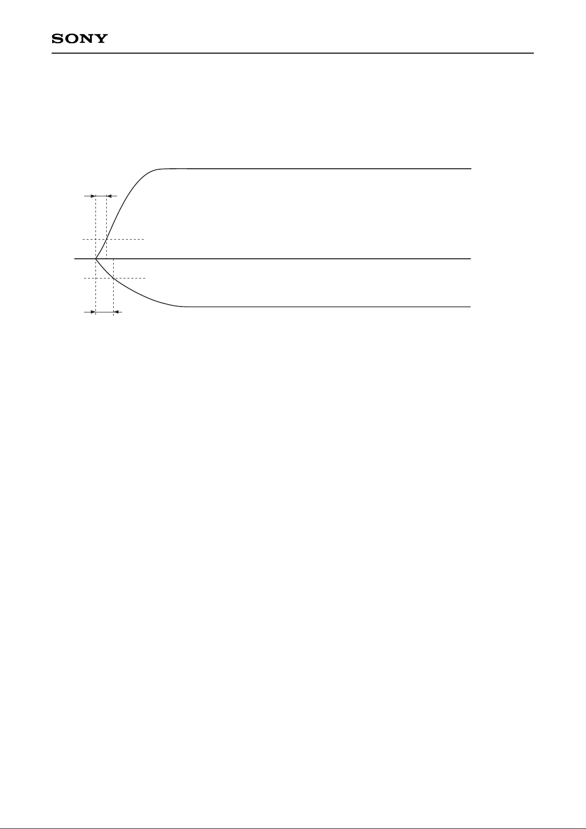
To avoid setting VSUB pin of the CCD image sensor negative potential, the former two power supplies should
be raised by the following order among three power supplies, –7.5V, +15.0V and +3.3V.
15.0V
20%
20%
t1
0V
–7.5V
t2
t2 ≥ t1
Page 37
– 37 –
CXD2457R
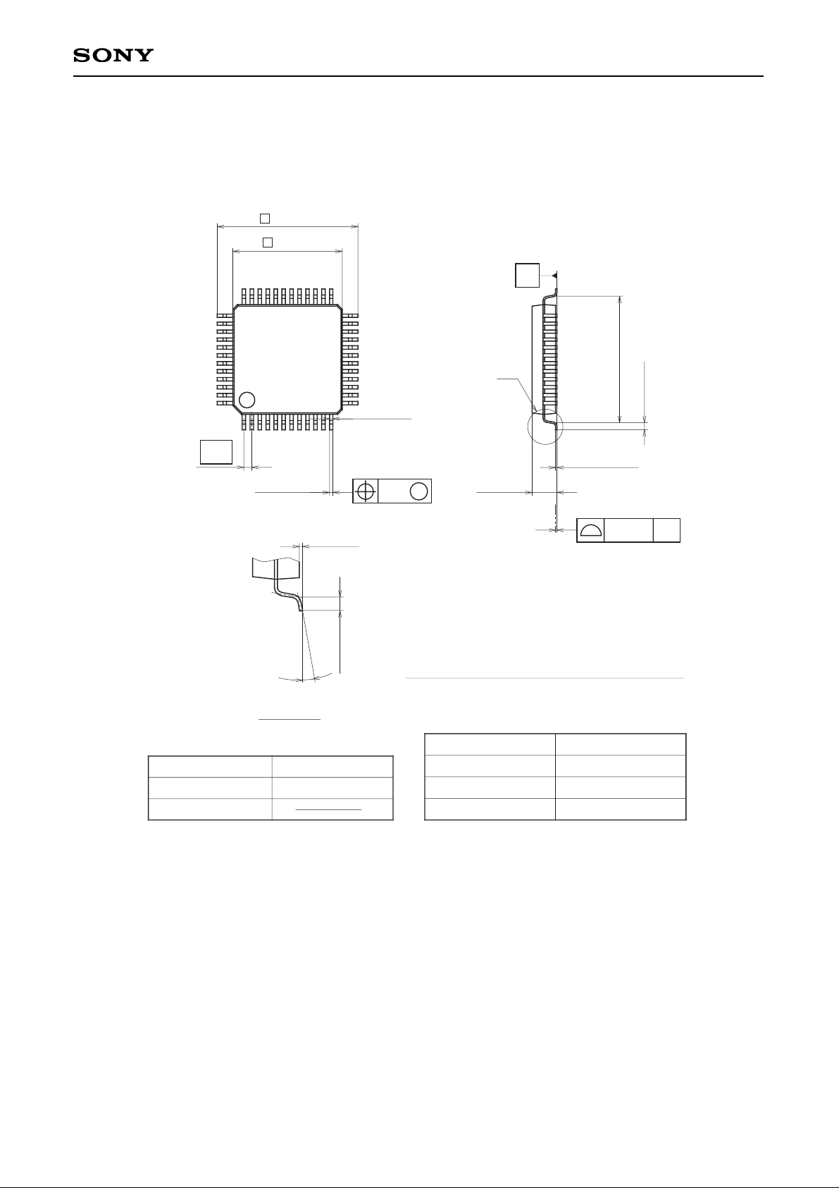
Package Outline Unit: mm
SONY CODE
EIAJ CODE
JEDEC CODE
PACKAGE MATERIAL
LEAD TREATMENT
LEAD MATERIAL
PACKAGE MASS
EPOXY RESIN
PLATING
42/COPPER ALLOY
PACKAGE STRUCTURE
48PIN LQFP (PLASTIC)
9.0 ± 0.2
∗ 7.0 ± 0.1
1
12
13
24
25
36
37
48
(0.22)
0.18 – 0.03
+ 0.08
0.2g
LQFP-48P-L01
LQFP048-P-0707
(8.0)
0.5 ± 0.2
0.127 – 0.02
+ 0.05
A
1.5 – 0.1
+ 0.2
0.1
SOLDER/PALLADIUM
NOTE: Dimension “∗” does not include mold protrusion.
0.1 ± 0.1
0.5 ± 0.2
0° to 10°
DETAIL A
0.13
M
0.5
S
S
 Loading...