

Page 1

Timing Generator for LCD Panels
Description
The CXD2443Q is a timing generator for the LCD
panel LCX011 and LCX019 driver. This chip has a
built-in serial interface circuit which allows various
settings to be performed through external control
from a microcomputer, etc.
Features
• Generates the LCD panel LCX011/LCX019 drive
pulse
• Supports NTSC/PAL
(PAL supported by scanning line conversion of
video signal to 525H or pulse eliminate.)
• Supports WIDE mode (when driving the LCX011)
• Supports HD mode (when driving the LCX011)
• Supports up/down and/or right/left inversion
• Supports 3-panel projectors
• Generates timing signal of external sample-and-
hold circuit
• Generates line inversion and field inversion signals
• AC drive of LCD panels during no signal
• Line double-speed display realized with a built-in
double-speed controller (NTSC/PAL) (4:3 mode only)
(Line memory µPD485505: NEC)
CXD2443Q
100 pin QFP (Plastic)
Absolute Maximum Ratings (Ta = 25°C, VSS = 0V)
• Supply voltage VDD VSS – 0.5 to +7.0 V
• Input voltage VI VSS – 0.5 to VDD + 0.5 V
• Output voltage VO VSS – 0.5 to VDD + 0.5 V
• Operating temperature
Topr –20 to +75 °C
• Storage temperature Tstg –55 to +150 °C
Recommended Operating Conditions
• Supply voltage VDD 4.5 to 5.5 V
• Operating temperature
Topr –20 to +75 °C
Applications
LCD projectors, etc.
Structure
Silicon CMOS IC
Sony reserves the right to change products and specifications without prior notice. This information does not convey any license by
any implication or otherwise under any patents or other right. Application circuits shown, if any, are typical examples illustrating the
operation of the devices. Sony cannot assume responsibility for any problems arising out of the use of these circuits.
– 1 –
E96X31-PS
Page 2

Block Diagram
CXD2443Q
RPD1
RPD2
RPD3
FPD1
FPD2
FPD3
HSYNC
VSYNC
VST
FLDO
VWA
VWB
SCTR
SCLK
SDAT
PRE
RPD4
FPD4
TC4
87
93
84
96
13
14
30
16
17
18
19
76
77
82
34
21
TC1
TC3
TC2
83
5
97
9
6
2
PHASE
COMPARATOR
H-SYNC DETECTOR
V-SYNC SEPARATOR
V-CONTROL COUNTER
V-POSITION COUNTER
PULSE ELIMINATOR
H-SYNC DETECTOR
PHASE
COMPARATOR
PLL COUNTER2
DECODER
71
70
98
DECODER
&
V-TIMING PULSE
GENERATOR
SERIAL I/F
72
73
CKI3
CKI5
CKSL
99
92
MASTER CLOCK
75
CKI2
CKO3
89
91
16 : 9 4 : 3HD
DOUBLE SCAN
CONVERTER
CLOCK2
74
CKI1
CKO2
88
11
PLL COUNTER
DECODER
FIELD & LINE
CONTROLLER
H-POSITION COUNTER
DECODER
H-TIMING PULSE
GENERATOR
LOOP
FILTER
81
80
44
10
&
CKO1
45
32
LOOP
FILTER
DIRECT
CLEAR
PWM1
8
86
PWM2
95
PWM3
PEO1
7
85
PEO2
94
PEO3
100
HDR
43
HSTA
HCK1A
38
37
HCK2A
ENB
36
35
VCK
49
FRP
50
XFRP
PCG1
31
XCLP1
47
48
XCLP2
46
PCG2
SH1A
51
SH2A
52
55
SH3A
56
SH4A
57
SH5A
58
SH6A
59
SH7A
HSTB
42
HCK1B
41
HCK2B
39
SH1B
61
62
SH2B
63
SH3B
64
SH4B
66
SH5B
67
SH6B
68
SH7B
1
RCK
WCK
RSTR
RSTW
TEST:12, 20, 22, 23, 24, 25, 26, 27, 33, 60, 69
DD: 3, 28, 53, 78
V
VSS: 4, 15, 29, 40, 54, 65, 79, 90
CKI4
CKO4
– 2 –
PEO4
PWM4
RGT
DWN
XRGT
XCLR
Page 3

Pin Description
CXD2443Q
Pin
No.
1
2
3
4
5
6
7
8
9
10
11
12
13
14
15
Symbol
XCLR
VWB
VDD
VSS
TC1
FPD1
PEO1
PWM1
RPD1
CKO1
CKI1
TEST2
HSYNC
VSYNC
VSS
I/O Description
I
System clear (Low: All clear)
O
V window pulse B output
—
Power supply
—
GND
I/O
FPD1 output pulse width adjustment (NTSC/PAL 4:3)
O
Phase comparator 1 output (NTSC/PAL 4:3)
I/O
Loop filter integrator 1 output (NTSC/PAL 4:3)
O
Loop filter integrator 1 input (NTSC/PAL 4:3)
O
Phase comparator 1 output (NTSC/PAL 4:3)
I/O
Oscillation cell 1 output (NTSC/PAL 4:3)
I
Oscillation cell 1 input (NTSC/PAL 4:3)
I
Test (Not connected.)
I
Horizontal sync signal input (Polarity set by serial data HPOL.)
I
Vertical sync signal input (Polarity set by serial data VPOL.)
—
GND
Input pin for
open status
H
—
—
—
—
—
—
—
—
—
—
—
—
—
—
16
17
18
19
20
21
22
23
24
25
26
27
28
29
30
31
32
SCTR
SCLK
SDAT
PRE
TEST11
FLDO
TEST1
TEST3
TEST4
TEST5
TEST6
TEST7
VDD
VSS
VWA
PCG1
DWN
I
Chip select input (serial transfer block)
I
Serial clock input (serial transfer block)
I
Serial data input (serial transfer block)
I
Preset setting (Set to NTSC 4:3 mode when Low.)
—
Test (Not connected.)
O
Field discrimination signal output
—
Test (Not connected.)
—
Test (Not connected.)
—
Test (Not connected.)
—
Test (Not connected.)
—
Test (Not connected.)
—
Test (Connect to GND.)
—
Power supply
—
GND
O
V window pulse A output
O
PCG1 pulse output (positive polarity)
O
Up/down inversion identification signal output (High: Down, Low: Up)
—
—
—
H
—
—
—
—
—
—
—
—
—
—
—
—
—
33
34
35
TEST8
VST
VCK
—
Test (Not connected.)
O
V start pulse output (positive polarity)
O
V clock pulse output
—
—
—
– 3 –
Page 4

CXD2443Q
Pin
No.
36
37
38
39
40
41
42
43
44
45
46
47
48
49
50
Symbol
ENB
HCK2A
HCK1A
HCK2B
VSS
HCK1B
HSTB
HSTA
RGT
XRGT
PCG2
XCLP1
XCLP2
FRP
XFRP
I/O Description
O
ENB pulse output (negative polarity)
O
H clock 2A pulse output
O
H clock 1A pulse output
O
H clock 2B pulse output
—
GND
O
H clock 1B pulse output
O
H start B pulse output (positive polarity)
O
H start A pulse output (positive polarity)
O
Right/left inversion identification signal output (High: Right, Low: Left)
O
Right/left inversion identification signal output (Low: Left, High: Right)
O
PCG2 pulse output (positive polarity)
O
Pedestal clamp pulse 1 output (negative polarity)
O
Pedestal clamp pulse 2 output (negative polarity)
O
AC drive inversion timing output
O
AC drive inversion timing output (reverse polarity of FRP)
Input pin for
open status
—
—
—
—
—
—
—
—
—
—
—
—
—
—
—
51
52
53
54
55
56
57
58
59
60
61
62
63
64
65
66
67
SH1A
SH2A
VDD
VSS
SH3A
SH4A
SH5A
SH6A
SH7A
TEST9
SH1B
SH2B
SH3B
SH4B
VSS
SH5B
SH6B
O
Sample-and-hold pulse 1A output (positive polarity)
O
Sample-and-hold pulse 2A output (positive polarity)
—
Power supply
—
GND
O
Sample-and-hold pulse 3A output (positive polarity)
O
Sample-and-hold pulse 4A output (positive polarity)
O
Sample-and-hold pulse 5A output (positive polarity)
O
Sample-and-hold pulse 6A output (positive polarity)
O
Sample-and-hold pulse 7A output (positive polarity)
—
Test (Not connected.)
O
Sample-and-hold pulse 1B output (positive polarity)
O
Sample-and-hold pulse 2B output (positive polarity)
O
Sample-and-hold pulse 3B output (positive polarity)
O
Sample-and-hold pulse 4B output (positive polarity)
—
GND
O
Sample-and-hold pulse 5B output (positive polarity)
O
Sample-and-hold pulse 6B output (positive polarity)
—
—
—
—
—
—
—
—
—
—
—
—
—
—
—
—
—
68
69
70
SH7B
TEST10
RCK
O
Sample-and-hold pulse 7B output (positive polarity)
—
Test (Not connected.)
O
Read clock output (for line buffer)
– 4 –
—
—
—
Page 5

CXD2443Q
Pin
No.
71
72
73
74
75
76
77
78
79
80
81
82
83
84
85
Symbol
RSTR
WCK
RSTW
CKO4
CKI4
RPD4
FPD4
VDD
VSS
PEO4
PWM4
TC4
TC2
FPD2
PEO2
I/O Description
O
Read reset output (for line buffer, negative polarity)
O
Write clock output (for line buffer)
O
Write reset output (for line buffer, negative polarity)
I/O
Oscillation cell 4 output (line double-speed controller)
I
Oscillation cell 4 input (line double-speed controller)
O
Phase comparator 4 output (line double-speed controller)
O
Phase comparator 4 output (line double-speed controller)
—
Power supply
—
GND
I/O
Loop filter integrator 4 output (line double-speed controller)
O
Loop filter integrator 4 input (line double-speed controller)
I/O
FPD4 output pulse width adjustment (line double-speed controller)
I/O
FPD2 output pulse width adjustment (NTSC/PAL 16:9)
O
Phase comparator 2 output (NTSC/PAL 16:9)
I/O
Loop filter integrator 2 output (NTSC/PAL 16:9)
Input pin for
open status
—
—
—
—
—
—
—
—
—
—
—
—
—
—
—
86
87
88
89
90
91
92
93
94
95
96
97
98
99
100
PWM2
RPD2
CKO2
CKI2
VSS
CKO3
CKI3
RPD3
PEO3
PWM3
FPD3
TC3
CKSL
CKI5
HDR
O
Loop filter integrator 2 input (NTSC/PAL 16:9)
O
Phase comparator 2 output (NTSC/PAL 16:9)
I/O
Oscillation cell 2 output (NTSC/PAL 16:9)
I
Oscillation cell 2 input (NTSC/PAL 16:9)
—
GND
I/O
Oscillation cell 3 output (HD)
I
Oscillation cell 3 input (HD)
O
Phase comparator 3 output (HD)
I/O
Loop filter integrator 3 output (HD)
O
Loop filter integrator 3 input (HD)
O
Phase comparator 3 output (HD)
I/O
FPD3 output pulse width adjustment (HD)
I
PLL system switching (High: Built-in PLL, Low: External PLL)
I
External clock input (for external phase comparison)
O
Phase comparator output (for external phase comparison)
—
—
—
—
—
—
—
—
—
—
—
—
H
—
—
∗
H: Pull up, L: Pull down
– 5 –
Page 6

CXD2443Q
Electrical Characteristics
1. DC characteristics (VDD = 5.0 ± 0.5V, VSS = 0V, Topr = –20 to +75°C)
Item
Supply voltage
Input, output voltages
Input voltage 1
Input voltage 2
Input voltage 3
Output voltage 1
Output voltage 2
Output voltage 3
Output voltage 4
Output voltage 5
Input leak current
Output leak current
Current consumption
∗1
XCLR, PRE, CKSL, CKI1, CKI2, CKI3, CKI4, CKI5, CKO1, CKO2, CKO3, CKO4, PWM1, PWM2, PWM3,
Symbol
VDD
VI, Vo
VIH
VIL
Vt+
Vt–
Vt+ – Vt–
Vt+
Vt–
Vt+ – Vt–
VOH
VOL
VOH
VOL
VOH
VOL
VOH
VOL
VOH
VOL
II
IIL
II
IOZ
IDD
CMOS input
TTL Schmitt
trigger input
CMOS Schmitt
trigger input
IOH = –2mA
IOL = 4mA
IOH = –4mA
IOL = 8mA
IOH = –4mA
IOL = 6mA
IOH = –3mA
IOL = 3mA
IOH = –12mA
IOL = 12mA
∗4
∗6
∗8
∗10
∗12
Min.
4.5
Vss
0.7VDD
2.2
0.8VDD
VDD – 0.8
VDD – 0.8
VDD – 0.8
VDD/2
VDD/2
–10
–40
–40
–40
Typ. Max. UnitConditions
5.0
0.4
0.6
–100
5.5
VDD
0.3VDD
0.8
0.2VDD
0.4
0.4
0.4
VDD/2
VDD/2
10
–240
40
40
110
V
V
V
V
V
V
V
V
V
V
µA
µA
mA
Applicable pins
∗1
HSYNC, SCTR,
VSYNC, SCLK,
SDAT
TC1, TC2, TC3,
TC4
∗2
∗3
RCK, WCK
PEO1, PEO2, PEO3,
PEO4, CKO4
CKO1, CKO2,
CKO3
∗5
∗7
∗9
∗11
At a 30pF load
PWM4, PEO1, PEO2, PEO3, PEO4
∗2
HDR, ENB, PCG1, PCG2, XCLP1, XCLP2, VST, FRP, XFRP, VCK, DWN, FLDO, RGT, XRGT, VWA,
VWB, RPD1, RPD2, RPD3, RPD4, FPD1, FPD2, FPD3, FPD4, TC1, TC2, TC3, TC4, RSTR, RSTW
∗3
HSTA, HCK1A, HCK2A, SH1A, SH2A, SH3A, SH4A, SH5A, SH6A, SH7A, HSTB, HCK1B, HCK2B, SH1B,
SH2B, SH3B, SH4B, SH5B, SH6B, SH7B
∗4
Normal input pins (VIN = VSS or VDD)
∗5
HSYNC, VSYNC, SCLK, SDAT, SCTR, CKI5
∗6
Pins with pull-up resistors (VIN = VSS)
∗7
PRE, XCLR, CKSL
∗8
Bidirectional pins (input status, VIN = VSS or VDD)
∗9
CKO1, CKO2, CKO3, CKO4, PEO1, PEO2, PEO3, PEO4, TC1, TC2, TC3, TC4
∗10
At high impedance (VIN = VSS or VDD)
∗11
RPD1, RPD2, RPD3, RPD4, FPD1, FPD2, FPD3, FPD4
∗12
fclk = 67MHz, VDD = 5.5V
∗13
HSTA, HSTB, HCK1A, HCK2A, HCK1B, HCK2B, SH1A, SH2A, SH3A, SH4A, SH5A, SH6A, SH7A, SH1B,
SH2B, SH3B, SH4B, SH5B, SH6B, SH7B, VCK, ENB, FRP, PCG1, PCG2, XCLP1, XCLP2, RGT, DWN
∗13
– 6 –
Page 7

CXD2443Q
2. AC characteristics (VDD = 5.0 ± 0.5V, Vss = 0V, Topr = –20 to +75°C)
Item
Clock input cycle
Output rise time
Output fall time
Cross-point time difference
Output rise delay time
Output fall delay time
HCK1 Duty
HCK2 Duty
∗1
HCK1A, 2A HCK1B, 2B
Symbol
tr
tf
∆t
tpr
tpf
tH/(tH + tL)
tL/(tH + tL)
Applicable pins
CKI1
CKI2
CKI3
CKI4
CKI5
All outputs
All outputs
∗1
All outputs
All outputs
HCK1A, HCK1B
HCK2A, HCK2B
Min. Typ.
21.3
16.0
15
28.2
15
–10
48
48
max. UnitConditions
20
20
10
15
15
52
52
CL = 30pF
CL = 30pF
CL = 30pF
CL = 30pF
CL = 30pF
CL = 30pF
CL = 30pF
ns
%
3. Serial transfer AC characteristics (VDD = 5.0 ± 0.5V, Vss = 0V, Topr = –20 to +75°C)
Symbol
ts0
ts1
th0
th1
tw1L
tw1H
tw2
tw3
Item
SCTR setup time, activated by rise of SCLK
SDAT setup time, activated by rise of SCLK
SCTR hold time, activated by rise of SCLK
SDAT hold time, activated by rise of SCLK
SCLK pulse width
SCLK pulse width
Min.
4T
2T
4T
2T
2T
2T
5T
5T
Typ. Max.
T: Master clock cycle (ns)
Unit
ns
– 7 –
Page 8

4. Timing definitions
AC characteristics
CXD2443Q
CKI1, CKI2
CKI3, CKI4
Output
Output
100%
HCK1A
HCK1B
HCK2A
HCK2B
tpr
10%
90%
tr
tf
90%
10%
tpf
50%
50% 50%
∆t∆t
50%
V
0V
V
0V
DD
DD
V
0V
V
0V
DD
DD
V
0V
DD
HCK1A
HCK1B
Note) HCK2 is the reverse phase of HCK1.
Serial transfer AC characteristics
ts0
SCTR 50%
tw1L tw1H
50%SCLK
ts1 th1 ts1 th1
SDAT
50%
D15 D8 D0
50%50% 50%
tw2
D14 D9 D7
tLtH
th0 tw3
50%
50%
D15
Note) See "Serial transfer timing" on P. 17 for the timing relationship between D15 to D0 and each pulse.
– 8 –
Page 9

B2
B2
B2
R2
R2
G2
G2
G2
B2
B2
R2
R2
R2
G2
G2
B1
B1
DR2
GATE SW
ODD = 13 dots
EVEN = 13 dots
DR1
GATE SW
• • • •
267
GATE SW
• • • •
ODD = 200 dots
EVEN = 200 dots
• • • •
GATE SW
234
GATE SW
• • • •
ODD = 1200 dots
EVEN = 1199 dots
ODD = 1626 dots
EVEN = 1626 dots
(effective 23.7501mm)
GATE SW
34
GATE SW
• • • •
2
GATE SW
ODD = 200 dots
EVEN = 200 dots
1
GATE SW
DL2
GATE SW
ODD = 13 dots
EVEN = 14 dots
DL1
GATE SW
LCX011 Dot Arrangement (1) (4:3 display)
The dot arrangement is a delta arrangement. Also, the shaded region in the diagram is not displayed.
R1 corresponds to SIG2, G1 to SIG1, B1 to SIG3, R2 to SIG5, G2 to SIG4 and B2 to SIG6.
G1
R1
B2
G2
R2
B1
G1
R1
B2
G2
R2
B1
G1
R1
B1
G1
R1
B2
G2
R2
B1
G1
R1
B2
G2
R2
B1
G1
R1
B2
G2
R2
B1
G1
R1
B2
G2
R2
B1
G1
R1
B2
G2
R2
B1
G1
R1
B2
G2
R2
B1
G1
R1
B2
G2
R2
B1
G1
R1
B2
G2
R2
B1
G1
R1
R1
B1
G1
R2
B2
G2
R1
B1
G1
R2
B2
G2
R1
B1
G1
R1
B1
G1
R2
B2
G2
R1
B1
G1
R2
B2
G2
R1
B1
G1
R2
B2
G2
R1
B1
G1
R2
B2
G2
R1
B1
G1
R2
B2
G2
R1
B1
G1
R2
B2
G2
R1
B1
G1
R2
B2
G2
R1
B1
G1
R2
B2
G2
R1
B1
G1
2 dots
R1
G1
B1
R1
G1
B2
R2
G2
B2
R2
G2
B1
R1
G1
B1
R1
G1
B2
R2
G2
B2
R2
G2
B1
R1
G1
B1
R1
G1
B1
R1
G1
B1
R1
G1
B2
R2
G2
B2
R2
G2
B1
R1
G1
B1
R1
G1
B2
R2
G2
B2
R2
G2
B1
R1
G1
B1
R1
G1
B2
R2
G2
B2
R2
G2
B1
R1
G1
B1
R1
G1
B2
R2
G2
B2
R2
G2
B1
R1
G1
B1
R1
G1
B2
R2
G2
B2
R2
G2
B1
R1
G1
B1
R1
G1
B2
R2
G2
B2
R2
G2
B1
R1
G1
B1
R1
G1
B2
R2
G2
B2
R2
G2
B1
R1
G1
B1
R1
G1
B2
R2
G2
B2
R2
G2
B1
R1
G1
B1
R1
G1
123
B1
G1
R1 G1 B1 R2 G2 B2
R1 G1 B1 R2 G2 B2
R1 G1 B1 R2 G2 B2
R1 G1 B1 R2 G2 B2
R1 G1 B1 R2 G2 B2
R1 G1 B1 R2 G2 B2
R1
G1 B1 R1 G2 B2 R2
G1 B1 R1 G2 B2 R2
G1 B1 R1 G2 B2 R2
G1 B1 R1 G2 B2 R2
B2
G2
R2
B1
G1
R1 G1 B1 R2 G2 B2
R1
B2
G2
R2
B1
G1
R1
B1
G1
R1
B2
G2
R2
B1
G1
R1
B2
G2
R2
B1
G1
R1
B2
G2
R2
B1
G1
R1
B2
G2
R2
B1
G1
R1
B2
G2
R2
B1
G1
R1
B2
G2
R2
B1
G1
R1
B2
G2
R2
B1
G1
R1
B2
G2
R2
B1
G1
R1
R1 G1 B1 R2 G2 B2
G1 B1 R1 G2 B2 R2
G1 B1 R1 G2 B2 R2
G1 B1 R1 G2 B2 R2
R1 G1 B1 R2 G2 B2
R1 G1 B1 R2 G2 B2
G1 B1 R1 G2 B2 R2
G1 B1 R1 G2 B2 R2
G1 B1 R1 G2 B2 R2
R1 G1 B1
R1 G1 B1
G1 B1 R1
G1 B1 R1
G1 B1 R1
R1 G1 B1 R2 G2 B2
R1 G1 B1 R2 G2 B2
G1 B1 R1 G2 B2 R2
G1 B1 R1 G2 B2 R2
G1 B1 R1 G2 B2 R2
R1 G1 B1 R2 G2 B2
R1 G1 B1 R2 G2 B2
G1 B1 R1 G2 B2 R2
G1 B1 R1 G2 B2 R2
G1 B1 R1 G2 B2 R2
R1 G1 B1 R2 G2 B2
R1 G1 B1 R2 G2 B2
G1 B1 R1 G2 B2 R2
G1 B1 R1 G2 B2 R2
G1 B1 R1 G2 B2 R2
R1 G1 B1 R2 G2 B2
R1 G1 B1 R2 G2 B2
G1 B1 R1 G2 B2 R2
G1 B1 R1 G2 B2 R2
G1 B1 R1 G2 B2 R2
R1 G1 B1 R2 G2 B2
R1 G1 B1 R2 G2 B2
G1 B1 R1 G2 B2 R2
G1 B1 R1 G2 B2 R2
G1 B1 R1 G2 B2 R2
R1 G1 B1 R2 G2 B2
R1 G1 B1 R2 G2 B2
G1 B1 R1 G2 B2 R2
G1 B1 R1 G2 B2 R2
G1 B1 R1 G2 B2 R2
R1 G1 B1 R2 G2 B2
R1 G1 B1 R2 G2 B2
G1 B1 R1 G2 B2 R2
G1 B1 R1 G2 B2 R2
G1 B1 R1 G2 B2 R2
R1 G1 B1 R2 G2 B2
R1 G1 B1 R2 G2 B2
G1 B1 R1 G2 B2 R2
G1 B1 R1 G2 B2 R2
G1 B1 R1 G2 B2 R2
G1 B1 R1 G2 B2 R2
R1 G1 B1 R2 G2 B2
R1 G1 B1 R2 G2 B2
R1 G1 B1 R2 G2 B2
G1 B1 R1 G2 B2 R2
G1 B1 R1 G2 B2 R2
R1 G1 B1 R2 G2 B2
R1 G1 B1 R2 G2 B2
R1 G1 B1 R2 G2 B2
G1 B1 R1 G2 B2 R2
G1 B1 R1 G2 B2 R2
R1 G1 B1
R1 G1 B1
R1 G1 B1
G1 B1 R1
G1 B1 R1
R1 G1 B1 R2 G2 B2
R1 G1 B1 R2 G2 B2
R1 G1 B1 R2 G2 B2
R1 G1 B1 R2 G2 B2
R1 G1 B1 R2 G2 B2
R1 G1 B1 R2 G2 B2
R1 G1 B1 R2 G2 B2
R1 G1 B1 R2 G2 B2
R1 G1 B1 R2 G2 B2
R1 G1 B1 R2 G2 B2
G1 B1 R1 G2 B2 R2
G1 B1 R1 G2 B2 R2
R1 G1 B1 R2 G2 B2
R1 G1 B1 R2 G2 B2
G1 B1 R1 G2 B2 R2
G1 B1 R1 G2 B2 R2
R1 G1 B1 R2 G2 B2
R1 G1 B1 R2 G2 B2
G1 B1 R1 G2 B2 R2
G1 B1 R1 G2 B2 R2
R1 G1 B1 R2 G2 B2
R1 G1 B1 R2 G2 B2
G1 B1 R1 G2 B2 R2
G1 B1 R1 G2 B2 R2
R1 G1 B1 R2 G2 B2
R1 G1 B1 R2 G2 B2
G1 B1 R1 G2 B2 R2
G1 B1 R1 G2 B2 R2
R1 G1 B1 R2 G2 B2
R1 G1 B1 R2 G2 B2
G1 B1 R1 G2 B2 R2
G1 B1 R1 G2 B2 R2
R1 G1 B1 R2 G2 B2
R1 G1 B1 R2 G2 B2
G1 B1 R1 G2 B2 R2
G1 B1 R1 G2 B2 R2
R1 G1 B1 R2 G2 B2
R1 G1 B1 R2 G2 B2
G1 B1 R1 G2 B2 R2
G1 B1 R1 G2 B2 R2
4
(effective 31.6701mm)
480 dots
R1 G1 B1 R2 G2 B2
G1 B1 R1 G2 B2 R2
G1 B1 R1 G2 B2 R2
G1 B1 R1 G2 B2 R2
R1 G1 B1 R2 G2 B2
R1 G1 B1 R2 G2 B2
G1 B1 R1 G2 B2 R2
G1 B1 R1 G2 B2 R2
G1 B1 R1 G2 B2 R2
R1 G1 B1 R2 G2 B2
R1 G1 B1 R2 G2 B2
G1 B1 R1 G2 B2 R2
G1 B1 R1 G2 B2 R2
G1 B1 R1 G2 B2 R2
R1 G1 B1
R1 G1 B1
G1 B1 R1
G1 B1 R1
G1 B1 R1
R1 G1 B1 R2 G2 B2
R1 G1 B1 R2 G2 B2
G1 B1 R1 G2 B2 R2
G1 B1 R1 G2 B2 R2
G1 B1 R1 G2 B2 R2
R1 G1 B1 R2 G2 B2
R1 G1 B1 R2 G2 B2
G1 B1 R1 G2 B2 R2
G1 B1 R1 G2 B2 R2
G1 B1 R1 G2 B2 R2
R1 G1 B1 R2 G2 B2
R1 G1 B1 R2 G2 B2
G1 B1 R1 G2 B2 R2
G1 B1 R1 G2 B2 R2
G1 B1 R1 G2 B2 R2
R1 G1 B1 R2 G2 B2
R1 G1 B1 R2 G2 B2
G1 B1 R1 G2 B2 R2
G1 B1 R1 G2 B2 R2
G1 B1 R1 G2 B2 R2
R1 G1 B1 R2 G2 B2
R1 G1 B1 R2 G2 B2
G1 B1 R1 G2 B2 R2
G1 B1 R1 G2 B2 R2
G1 B1 R1 G2 B2 R2
R1 G1 B1 R2 G2 B2
R1 G1 B1 R2 G2 B2
G1 B1 R1 G2 B2 R2
G1 B1 R1 G2 B2 R2
G1 B1 R1 G2 B2 R2
R1 G1 B1 R2 G2 B2
R1 G1 B1 R2 G2 B2
G1 B1 R1 G2 B2 R2
G1 B1 R1 G2 B2 R2
G1 B1 R1 G2 B2 R2
R1 G1 B1 R2 G2 B2
R1 G1 B1 R2 G2 B2
G1 B1 R1 G2 B2 R2
G1 B1 R1 G2 B2 R2
G1 B1 R1 G2 B2 R2
479
480
2 dots
SID
PC
VDD
PCX
CXD2443Q
WD
VSS
WDX
JTN
JTP
– 9 –
Page 10

B2
B2
B2
R2
R2
G2
G2
G2
B2
B2
R2
R2
R2
G2
G2
B1
B1
DR2
GATE SW
ODD = 13 dots
EVEN = 13 dots
DR1
GATE SW
• • • •
267
GATE SW
• • • •
• • • •
GATE SW
234
GATE SW
• • • •
ODD = 1600 dots
EVEN = 1599 dots
ODD = 1626 dots
EVEN = 1626 dots
(effective 31.6701mm)
GATE SW
34
GATE SW
• • • •
2
GATE SW
1
GATE SW
DL2
GATE SW
ODD = 13 dots
EVEN = 14 dots
DL1
GATE SW
LCX011 Dot Arrangement (2) (16:9 display)
The dot arrangement is a delta arrangement. Also, the shaded region in the diagram is not displayed.
R1 corresponds to SIG2, G1 to SIG1, B1 to SIG3, R2 to SIG5, G2 to SIG4 and B2 to SIG6.
G1
R1
B2
G2
R2
B1
G1
R1
B2
G2
R2
B1
G1
R1
B1
G1
R1
B2
G2
R2
B1
G1
R1
B2
G2
R2
B1
G1
R1
B2
G2
R2
B1
G1
R1
B2
G2
R2
B1
G1
R1
B2
G2
R2
B1
G1
R1
B2
G2
R2
B1
G1
R1
B2
G2
R2
B1
G1
R1
B2
G2
R2
B1
G1
R1
R1
B1
G1
R2
B2
G2
R1
B1
G1
R2
B2
G2
R1
B1
G1
R1
B1
G1
R2
B2
G2
R1
B1
G1
R2
B2
G2
R1
B1
G1
R2
B2
G2
R1
B1
G1
R2
B2
G2
R1
B1
G1
R2
B2
G2
R1
B1
G1
R2
B2
G2
R1
B1
G1
R2
B2
G2
R1
B1
G1
R2
B2
G2
R1
B1
G1
2 dots
R1
G1
B1
R1
G1
B2
R2
G2
B2
R2
G2
B1
R1
G1
B1
R1
G1
B2
R2
G2
B2
R2
G2
B1
R1
G1
B1
R1
G1
B1
R1
G1
B1
R1
G1
B2
R2
G2
B2
R2
G2
B1
R1
G1
B1
R1
G1
B2
R2
G2
B2
R2
G2
B1
R1
G1
B1
R1
G1
B2
R2
G2
B2
R2
G2
B1
R1
G1
B1
R1
G1
B2
R2
G2
B2
R2
G2
B1
R1
G1
B1
R1
G1
B2
R2
G2
B2
R2
G2
B1
R1
G1
B1
R1
G1
B2
R2
G2
B2
R2
G2
B1
R1
G1
B1
R1
G1
B2
R2
G2
B2
R2
G2
B1
R1
G1
B1
R1
G1
B2
R2
G2
B2
R2
G2
B1
R1
G1
B1
R1
G1
123
B1
G1
R1 G1 B1 R2 G2 B2
R1 G1 B1 R2 G2 B2
R1 G1 B1 R2 G2 B2
R1 G1 B1 R2 G2 B2
R1 G1 B1 R2 G2 B2
R1 G1 B1 R2 G2 B2
R1
G1 B1 R1 G2 B2 R2
G1 B1 R1 G2 B2 R2
G1 B1 R1 G2 B2 R2
G1 B1 R1 G2 B2 R2
B2
G2
R2
B1
G1
R1 G1 B1 R2 G2 B2
R1
B2
G2
R2
B1
G1
R1
B1
G1
R1
B2
G2
R2
B1
G1
R1
B2
G2
R2
B1
G1
R1
B2
G2
R2
B1
G1
R1
B2
G2
R2
B1
G1
R1
B2
G2
R2
B1
G1
R1
B2
G2
R2
B1
G1
R1
B2
G2
R2
B1
G1
R1
B2
G2
R2
B1
G1
R1
R1 G1 B1 R2 G2 B2
G1 B1 R1 G2 B2 R2
G1 B1 R1 G2 B2 R2
G1 B1 R1 G2 B2 R2
R1 G1 B1 R2 G2 B2
R1 G1 B1 R2 G2 B2
G1 B1 R1 G2 B2 R2
G1 B1 R1 G2 B2 R2
G1 B1 R1 G2 B2 R2
R1 G1 B1
R1 G1 B1
G1 B1 R1
G1 B1 R1
G1 B1 R1
R1 G1 B1 R2 G2 B2
R1 G1 B1 R2 G2 B2
G1 B1 R1 G2 B2 R2
G1 B1 R1 G2 B2 R2
G1 B1 R1 G2 B2 R2
R1 G1 B1 R2 G2 B2
R1 G1 B1 R2 G2 B2
G1 B1 R1 G2 B2 R2
G1 B1 R1 G2 B2 R2
G1 B1 R1 G2 B2 R2
R1 G1 B1 R2 G2 B2
R1 G1 B1 R2 G2 B2
G1 B1 R1 G2 B2 R2
G1 B1 R1 G2 B2 R2
G1 B1 R1 G2 B2 R2
R1 G1 B1 R2 G2 B2
R1 G1 B1 R2 G2 B2
G1 B1 R1 G2 B2 R2
G1 B1 R1 G2 B2 R2
G1 B1 R1 G2 B2 R2
R1 G1 B1 R2 G2 B2
R1 G1 B1 R2 G2 B2
G1 B1 R1 G2 B2 R2
G1 B1 R1 G2 B2 R2
G1 B1 R1 G2 B2 R2
R1 G1 B1 R2 G2 B2
R1 G1 B1 R2 G2 B2
G1 B1 R1 G2 B2 R2
G1 B1 R1 G2 B2 R2
G1 B1 R1 G2 B2 R2
R1 G1 B1 R2 G2 B2
R1 G1 B1 R2 G2 B2
G1 B1 R1 G2 B2 R2
G1 B1 R1 G2 B2 R2
G1 B1 R1 G2 B2 R2
R1 G1 B1 R2 G2 B2
R1 G1 B1 R2 G2 B2
G1 B1 R1 G2 B2 R2
G1 B1 R1 G2 B2 R2
G1 B1 R1 G2 B2 R2
G1 B1 R1 G2 B2 R2
R1 G1 B1 R2 G2 B2
R1 G1 B1 R2 G2 B2
R1 G1 B1 R2 G2 B2
G1 B1 R1 G2 B2 R2
G1 B1 R1 G2 B2 R2
R1 G1 B1 R2 G2 B2
R1 G1 B1 R2 G2 B2
R1 G1 B1 R2 G2 B2
G1 B1 R1 G2 B2 R2
G1 B1 R1 G2 B2 R2
R1 G1 B1
R1 G1 B1
R1 G1 B1
G1 B1 R1
G1 B1 R1
R1 G1 B1 R2 G2 B2
R1 G1 B1 R2 G2 B2
R1 G1 B1 R2 G2 B2
G1 B1 R1 G2 B2 R2
G1 B1 R1 G2 B2 R2
R1 G1 B1 R2 G2 B2
R1 G1 B1 R2 G2 B2
R1 G1 B1 R2 G2 B2
G1 B1 R1 G2 B2 R2
G1 B1 R1 G2 B2 R2
R1 G1 B1 R2 G2 B2
R1 G1 B1 R2 G2 B2
R1 G1 B1 R2 G2 B2
G1 B1 R1 G2 B2 R2
G1 B1 R1 G2 B2 R2
R1 G1 B1 R2 G2 B2
R1 G1 B1 R2 G2 B2
R1 G1 B1 R2 G2 B2
G1 B1 R1 G2 B2 R2
G1 B1 R1 G2 B2 R2
R1 G1 B1 R2 G2 B2
R1 G1 B1 R2 G2 B2
R1 G1 B1 R2 G2 B2
G1 B1 R1 G2 B2 R2
G1 B1 R1 G2 B2 R2
R1 G1 B1 R2 G2 B2
R1 G1 B1 R2 G2 B2
R1 G1 B1 R2 G2 B2
R1 G1 B1 R2 G2 B2
R1 G1 B1 R2 G2 B2
G1 B1 R1 G2 B2 R2
G1 B1 R1 G2 B2 R2
R1 G1 B1 R2 G2 B2
R1 G1 B1 R2 G2 B2
G1 B1 R1 G2 B2 R2
G1 B1 R1 G2 B2 R2
R1 G1 B1 R2 G2 B2
R1 G1 B1 R2 G2 B2
G1 B1 R1 G2 B2 R2
G1 B1 R1 G2 B2 R2
4
(effective 31.6701mm)
480 dots
R1 G1 B1 R2 G2 B2
G1 B1 R1 G2 B2 R2
G1 B1 R1 G2 B2 R2
G1 B1 R1 G2 B2 R2
R1 G1 B1 R2 G2 B2
R1 G1 B1 R2 G2 B2
G1 B1 R1 G2 B2 R2
G1 B1 R1 G2 B2 R2
G1 B1 R1 G2 B2 R2
R1 G1 B1 R2 G2 B2
R1 G1 B1 R2 G2 B2
G1 B1 R1 G2 B2 R2
G1 B1 R1 G2 B2 R2
G1 B1 R1 G2 B2 R2
R1 G1 B1
R1 G1 B1
G1 B1 R1
G1 B1 R1
G1 B1 R1
R1 G1 B1 R2 G2 B2
R1 G1 B1 R2 G2 B2
G1 B1 R1 G2 B2 R2
G1 B1 R1 G2 B2 R2
G1 B1 R1 G2 B2 R2
R1 G1 B1 R2 G2 B2
R1 G1 B1 R2 G2 B2
G1 B1 R1 G2 B2 R2
G1 B1 R1 G2 B2 R2
G1 B1 R1 G2 B2 R2
R1 G1 B1 R2 G2 B2
R1 G1 B1 R2 G2 B2
G1 B1 R1 G2 B2 R2
G1 B1 R1 G2 B2 R2
G1 B1 R1 G2 B2 R2
R1 G1 B1 R2 G2 B2
R1 G1 B1 R2 G2 B2
G1 B1 R1 G2 B2 R2
G1 B1 R1 G2 B2 R2
G1 B1 R1 G2 B2 R2
R1 G1 B1 R2 G2 B2
R1 G1 B1 R2 G2 B2
G1 B1 R1 G2 B2 R2
G1 B1 R1 G2 B2 R2
G1 B1 R1 G2 B2 R2
R1 G1 B1 R2 G2 B2
R1 G1 B1 R2 G2 B2
G1 B1 R1 G2 B2 R2
G1 B1 R1 G2 B2 R2
G1 B1 R1 G2 B2 R2
R1 G1 B1 R2 G2 B2
R1 G1 B1 R2 G2 B2
G1 B1 R1 G2 B2 R2
G1 B1 R1 G2 B2 R2
G1 B1 R1 G2 B2 R2
R1 G1 B1 R2 G2 B2
R1 G1 B1 R2 G2 B2
G1 B1 R1 G2 B2 R2
G1 B1 R1 G2 B2 R2
G1 B1 R1 G2 B2 R2
479
480
2 dots
SID
PC
VDD
PCX
– 10 –
CXD2443Q
WD
VSS
WDX
JTN
JTP
Page 11

DR1
GATE SW
CXD2443Q
ODD = 1200 dots
EVEN = 1199 dots
DL2
GATE SW
201
GATE SW
GATE SW
1
GATE SW
RGBRGBRGB
RGBRGBRGB
RGBRGBRGBRGB
GB
R
RGB
RGBRGBRGBRGB
RGBRGBRGBRGB
GB
RGBRGBRGB
RGBRGBRGBRGB
GB
R
RGB
RGBRGBRGBRGB
RGBRGBRGBRGB
GB
RGBRGBRGB
RGBRGBRGB
RGBRGBRGB
RGBRGBRGB
RGBRGBRGBRGB
GB
R
RGB
RGBRGBRGBRGB
RGBRGBRGBRGB
GB
RGBRGBRGB
RGBRGBRGBRGB
GB
R
RGB
RGBRGBRGBRGB
RGBRGBRGBRGB
GB
RGBRGBRGBRGB
GB
R
RGB
RGBRGBRGBRGB
RGBRGBRGBRGB
GB
RGBRGBRGB
RGBRGBRGBRGB
RGBRGBRGBRGB
RGBRGBRGBRGB
RGB
RGBRGBRGBRGB
RGBRGBRGBRGB
GB
R
RGB
RGBRGBRGBRGB
RGBRGBRGBRGB
GB
RGBRGBRGBRGB
RGB
RGBRGBRGBRGB
RGBRRGBRRGBRRGBRRGBRRGBRRGBRRGBRRGBRRGB
GB
R
RGB
RGBRGBRGBRGB
RGBRGBRGBRGB
GB
GB
R
RGB
RGBRGBRGBRGB
RGBRGBRGBRGB
GB
GB
R
RGBRGBRGBRGB
GB
RGBRGBRGB
GB
R
RGBRGBRGBRGB
GB
R
DR2
GATE SW
DR1
RGBRGBRGBRGB
RGBRGBRGBRGB
RGBRGBRGBRGB
RGBRGBRGBRGB
RGBRGBRGBRGB
RGBRGBRGBRGB
RGBRGBRGBRGB
RGBRGBRGBRGB
RGBRGBRGBRGB
RGBRGBRGBRGB
GATE SW
RGBRGBRGBRGB
RGBRGBRGBRGB
RGBRGBRGBRGB
RGBRGBRGBRGB
RGBRGBRGBRGB
RGBRGBRGBRGB
RGBRGBRGBRGB
RGBRGBRGBRGB
RGBRGBRGBRGB
479
RGBRGBRGBRGB
GB
R
480
GB
R
2 dots
GB
GB
GB
GB
GB
GB
GB
GB
R
R
R
R
R
R
R
R
1
2
3
4
2 dots
LCX019 Dot Arrangement
The dot arrangement is a delta arrangement. Also, the shaded region in the diagram is not displayed.
R1 corresponds to SIG2, G1 to SIG1, B1 to SIG3, R2 to SIG5, G2 to SIG4 and B2 to SIG6.
480 dots
– 11 –
PSIG
PC
PCX
Page 12

CXD2443Q
Input Signal Protocol
1. Horizontal sync signal
• A double-speed HSYNC or standard HSYNC (or CSYNC) should be input for NTSC and PAL display modes.
Double-speed HSYNC and standard HSYNC input switching is set by the serial data (SNSL).
Note) The double-speed HSYNC should have a cycle and width 1/2 that of the standard HSYNC.
• The signal obtained by cutting off only the bottom of the ternary SYNC should be input for HD display mode.
• The input sync signal polarity is not fixed, and is set by the serial data (HPOL).
• When using the built-in line double-speed controller, set serial data SNSL to Low. The built-in line double-
speed controller supports only the standard HSYNC (or CSYNC).
2. Vertical sync signal
• A normal-speed VSYNC (or CSYNC) should be input for NTSC and PAL display modes.
• A VSYNC that has been sync separated by SYNC SEP. should be input for HD display mode.
• The input sync signal polarity is not fixed, and is set by the serial data (VPOL).
• The phase relationship between HSYNC and VSYNC is specified as follows for the CXD2443Q.
(1) Double-speed NTSC
Double-speed HSYNC
(2) Double-speed PAL
Double-speed HSYNC
(3) NTSC (CSYNC input)
ODD FIELD
CSYNC
EVEN FIELD
CSYNC
(4) PAL (CSYNC input)
ODD FIELD
CSYNC
EVEN FIELD
CSYNC
VSYNC
VSYNC
Sync signal phase
reference
Sync signal phase
reference
Sync signal phase reference
Sync signal phase reference
(5) HD
ODD FIELD
HSYNC
VSYNC
EVEN FIELD
HSYNC
VSYNC
Sync signal phase
reference
Sync signal phase
reference
– 12 –
Page 13

Description of Operation
Clock input
The CXD2443Q supports two types of PLL circuits.
PLL switching is performed by CKSL (Pin 98). (High: Built-in PLL, Low: External PLL)
Note) The built-in line double-speed controller PLL is supported only by the built-in PLL.
(1) Built-in PLL (CKI1, CKI2, CKI3, CKI4)
A PLL circuit is comprised by the built-in phase comparator and an external VCO circuit. There are four
clock inputs which support the following modes.
CKI1: NTSC/PAL 4:3 CKI2: NTSC/PAL 16:9
CKI3: HD CKI4: For built-in line double-speed controller
The PLL lock for this system is adjusted by setting the RPD and FPD transition points so that they fall at
the center of the windows as shown in the diagram below. (See the Application Circuit.)
aa
HSYNC
CXD2443Q
RPD
FPD
bb
Output waveform during PLL lock
800ns
(2) External PLL (CKI5)
The CKI5 pin is the clock input pin when using an external PLL IC. The 1/N frequency divider output is
output from the HDR pin (frequency division ratio N/2) for the PLL IC. Set CKSL (Pin 98) to Low to switch to
the external PLL.
H
N f
HSYNC
HDR
N/2 fH
AC driving of LCD panels for no signal
The following measures have been adopted to allow AC driving of LCD panels even when there is no signal.
• Horizontal direction pulse
The PLL is set to free running status. The frequency of the horizontal direction pulse at this time is dependent
on the PLL free running frequency.
• Vertical direction pulse
The number of lines is counted by an internal counter and the vertical direction pulses (VST, FRP) are output
at a specified cycle. For the CXD2443Q, no signal (free running) status is judged if there is no VSYNC input
for longer than the following (free running detection) periods.
Mode
NTSC
PAL
HD
V cycle for no signal
544H (272H)
640H (320H)
576H
Free running detection
1024H (512H)
Note) Numbers in parentheses are for when using the built-in line double-speed controller.
– 13 –
Page 14

CXD2443Q
Right/left and/or up/down inversion
In delta arrangement LCD panels, the same signal lines are separated by 1.5 dots for each horizontal line.
Therefore, a 1.5 dot offset is added between lines to the LCD's horizontal direction start pulses HST and HCK
and sample-and-hold pulse (SH).
When driving an LCD panel with right and left inversed, the dot arrangement is asymmetrical so an offset is
attached to HST, HCK and SH. When driving with up and down inversed, the relationship between the panel's
odd and even line offsets is reversed.
Right scan Left scan
H SCANNER
Down scan
Effective display area
V SCANNER
MCK
HST
Up scan
1.5fH
1.5fH
Down scan, odd line
Up scan, even line
Right and down scan, even line
Right and up scan, odd line
Left and down scan, even line
Left and up scan, odd line
– 14 –
Page 15

CXD2443Q
When using three LCD panels
B outputs (HSTB, HCK1B, HCK2B, SH1B to 7B) are provided for driving three LCD panels with and without
right/left inversion at the same time. These B outputs are the right/left inversed timings of the A outputs (HSTA,
HCK1A, HCK2A, SH1A to 7A).
XRGT (RGT inversed output) is also provided for right/left inversion scanning.
Application circuit (driving three LCD panels)
TG
Right scan
(A outputs)
Left scan
(B outputs)
SH1A
SH2A
SH3A
SH4A
SH5A
SH6A
SH7A
HSTA
HCK1A
HCK2A
RGT
SH1B
SH2B
SH3B
SH4B
SH5B
SH6B
SH7B
HSTB
HCK1B
HCK2B
XRGT
51
52
55
56
57
58
59
43
38
37
44
61
62
63
64
66
67
68
42
41
39
45
SIGNAL DRIVER
SIGNAL DRIVER
SIGNAL DRIVER
Panel 1
(right scan)
Panel 2
(right scan)
Panel 3
(left scan)
Common
DWN
PCG1
or
PCG2
ENB
VCK
VST
32
36
35
31
46
34
Note) All three panels face the same direction.
– 15 –
Page 16

CXD2443Q
Built-in line double-speed controller
This controller is designed to use the µPD485505 (NEC/high-speed line buffer) as the system line memory IC,
and generates the double-speed processing pulses RSTW (reset write), WCK (write clock), RSTR (reset read)
and RCK (read clock).
Operation is as follows. Write operation is started at the RSTW timing, and this memory information is read
twice at double speed at the RSTR timing which is delayed by 1/2H and 1H from the RSTW timing. The write
and read clock frequencies at this time are generated by the built-in PLL (CKI4).
See the specifications for a detailed description of µPD485505 operation.
R, G, B IN
HSYNC
RSTW
WCK
RSTR
RCK
ADC DAC
RSTW
WCK
HSYNC
VSYNC
CSYNC
Double-speed display system block
LINE Mem.
µPD485505
RSTR
RCK
CXD2443Q
MCK : f
f/2
f
HSYNC
RSTW
RSTR
Note) See the timing charts for details.
Double-speed display timing
– 16 –
Page 17

CXD2443Q
XCLR pin
The CXD2443Q should be forcibly reset during power on in order to initialize the serial transfer block and other
internal circuits.
Serial transfer operation
1. Control method
The CXD2443Q operation timing is controlled by serial data.
The control data is comprised of an 8-bit address and 8-bit data, and the individual data is fetched at the rise
of SCLK. This fetching operation starts from the fall of SCTR and is completed at the next rise of SCTR.
Serial transfer timing
SCTR
SCLK
D15 D14 D13 D12 D11 D10 D9 D8 D7 D6 D5 D4 D3 D2 D1 D0SDAT
Address Data
2. Control data
When using the CXD2443Q, set the control data corresponding to each signal source according to the formats
in the table below.
Address
Data
Function
D15
D14D13
0
0
0
0
0
0
0
0
0
0
0
0
0
0
0
0
0
0
D12
D11D10
0
0
0
0
0
0
0
0
0
0
0
0
0
0
0
0
0
0
0
0
0
0
0
0
0
0
1
D9 D8 D7 D6 D5 D4 D3 D2 D1 D0
0
0
0
HP8
HP7
0
0
1
—
0
1
0
—
0
1
1
—
1
0
0
—
1
0
1
—
1
1
0
VM7J
1
1
1
0
0
0
VM7K
VM6J
—
VM6K
—
—
—
—
—
—
HP6
—
—
—
—
—
VM5J
—
VM5K
HP5
—
—
—
—
—
VM4J
—
VM4K
HP4
VP4
SLSH4
—
—
—
VM3J
—
VM3K
HP3
VP3
SLSH3
—
—
—
VM2J
—
VM2K
HP2
VP2
SLSH2
CP2
PCGW2
VM9J
VM1J
VM9K
VM1K
HP1
VP1
SLSH1
CP1
PCGW1
VM8J
VM0J
VM8K
VM0K
(A) H-POSITION
(B) V-POSITION
(C) SH-POSITION
(D) XCLP-POSITION
(E) PCG-POSITION
(F) VWA-POSITION
(VWA pulse)
0
0
0
0
1
0
0
1
—
0
0
0
0
1
0
1
0
—
0
0
0
0
1
0
1
1
—
0
0
0
0
1
1
0
0
—
0
0
0
0
1
1
0
1
—
0
0
0
0
1
1
1
0
—
—
—
—
—
—
—
—
—
—
TEST4
—
—
—
—
—
TEST3
—
—
—
—
—
SL3B
—
SNSL
Note) 1. Set "High" as the TEST1, TEST2, TEST3 and TEST4 data.
2. "—" indicates not set.
– 17 –
—
—
—
VPOL
—
XHD
TEST1
MA
DWN
HPOL
SLVWB
XWID
SLBA
TEST2
RGT
SLFR
SLEG
NT-PAL
(G) Double-speed
setting
(H) Double-speed
PAL pulse eliminate
(I) Right/left and/or
up/down inversion
(J) Various settings
(K) Mode settings
Page 18

CXD2443Q
Serial settings during power on
The CXD2443Q should be forcibly reset during power on using the XCLR pin. After being forcibly reset, the
master clock for the CXD2443Q is supplied from CKI3. The initial serial data after power on is loaded to the
CXD2443Q using the clock from CKI3.
Serial settings during PLL free running
When the PLL is in free running status, the serial clock cycle (F ns) may be less than F ≥ 2T with respect to the
master clock cycle (T ns). Take care that the serial clock cycle setting is such that F ≥ 2T during PLL free
running.
Each control data is described in detail below.
(A) H-POSITION
(HP1, HP2, HP3, HP4, HP5, HP6, HP7, HP8)
These bits set the horizontal display start position. The minimum adjustment width is 1 dot, and adjustment of
up to ±128 dots is possible with respect to the design center value. (data: 8 bits)
Design center value HP1 HP2 HP3 HP4 HP5 HP6 HP7 HP8
LLLLLLLH
MODE Variable time (±128fH)
NTSC (4:3)
NTSC (16:9)
PAL (4:3)
PAL (16:9)
HD
±2.8µs
±2.1µs
±2.7µs
±2.0µs
±1.9µs
(B) V-POSITION
(VP1, VP2, VP3, VP4)
These bits set the vertical display start position. The minimum adjustment width is 1H, and adjustment of up to
±8H is possible with respect to the design center value. (data: 4 bits)
Design center value VP1 VP2 VP3 VP4
LLLH
– 18 –
Page 19
CXD2443Q
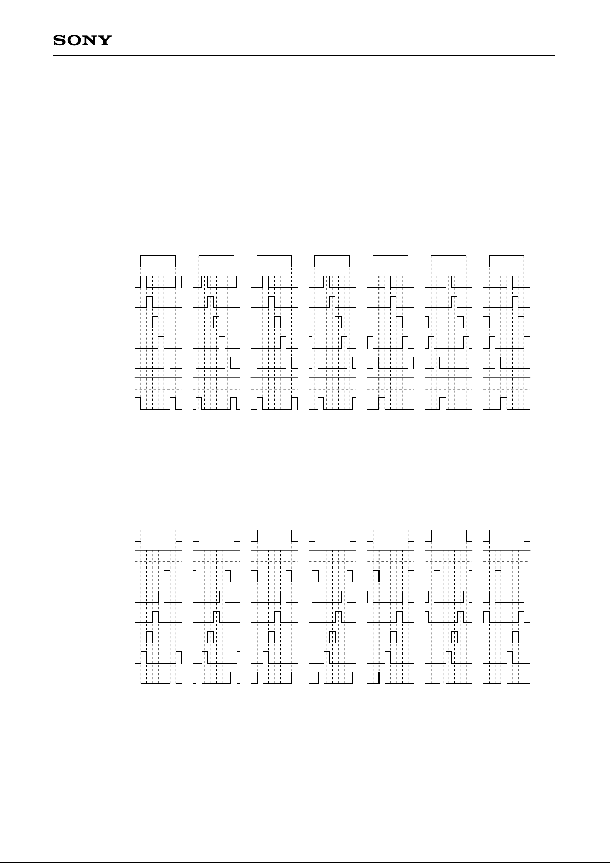
(C) SH-POSITION
(SLSH1, SLSH2, SLSH3, SLSH4)
These bits control the phase relationship between HCK1, HCK2 and SH1, 2, 3, 4, 5, 6 and 7. The minimum
adjustment width is 0.5 dots, and adjustment of up to 6 dots is possible. (data: 4 bits)
RGT = High: A output
RGT = Low: B output
SLSH1, 2, 3, 4 LLLL (0) HLLL (1) LHLL (2) HHLL (3) LLHL (4) HLHL (5) LHHL (6)
HCKn
SH1
SH2
SH3
SH4
SH5
SH6
SH7
RGT = Low: A output
RGT = High: B output
HCKn
SH1
SH2
SH3
SH4
SH5
SH6
SH7
– 19 –
Page 20
RGT = High: A output
RGT = Low: B output
CXD2443Q
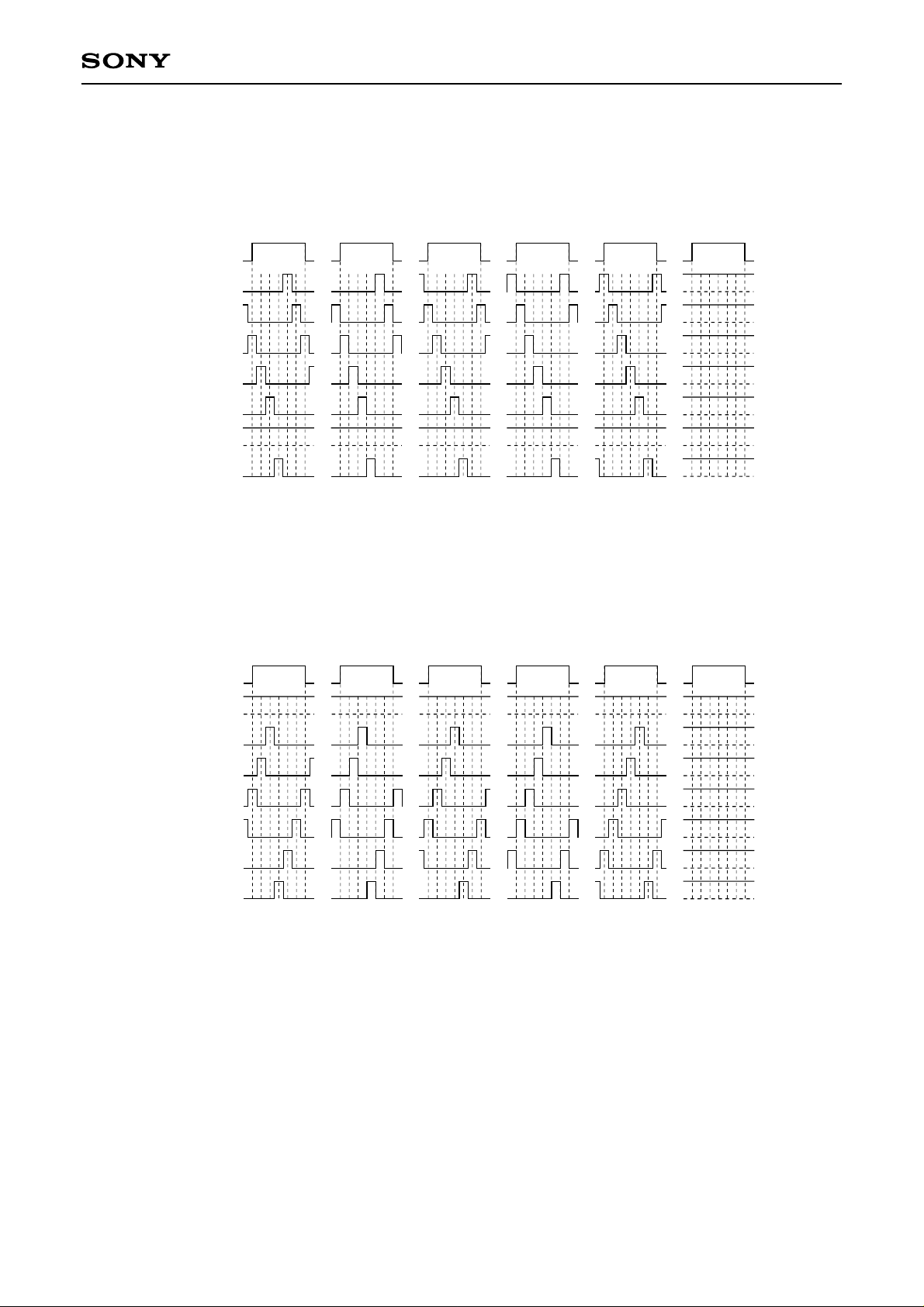
SLSH1, 2, 3, 4 HHHL (7) LLLH (8) HLLH (9) LHLH (A) HHLH (B)
HCKn
SH1
SH2
SH3
SH4
SH5
SH6
SH7
RGT = Low: A output
RGT = High: B output
∗∗HH (C, D, E, F)
HCKn
SH1
SH2
SH3
SH4
SH5
SH6
SH7
– 20 –
Page 21
CXD2443Q
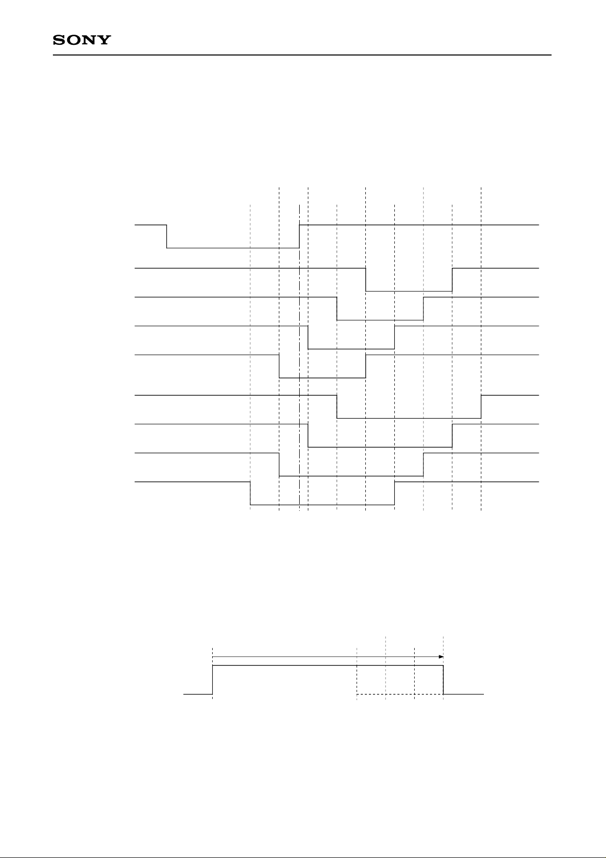
(D) XCLP-POSITION
(CP1, CP2)
These bits control the phase relationship between pedestal clamp pulses XCLP1 and XCLP2 and HSYNC. The
phase can be adjusted in 400ns units to four levels. (data: 2 bits)
–250ns0150ns 950ns 1750ns 2550ns
HSYNC
XCLP1
CP1 = H, CP2 = H
CP1 = L, CP2 = H (design center value)
CP1 = H, CP2 = L
CP1 = L, CP2 = L
XCLP2
CP1 = H, CP2 = H
CP1 = L, CP2 = H (design center value)
CP1 = H, CP2 = L
CP1 = L, CP2 = L
–650ns
550ns 1350ns 2150ns
(E) PCG-POSITION
(PCGW1, PCGW2)
These bits control the PCG1 pulse width (falling edge). The width can be adjusted in 200ns units to four levels.
(data: 2 bits)
PCG pulse
Fixed
1.4µs
1.2µs
LL HL LHPCGW1, 2 = HH
1.8µs
1.6µs
– 21 –
Page 22
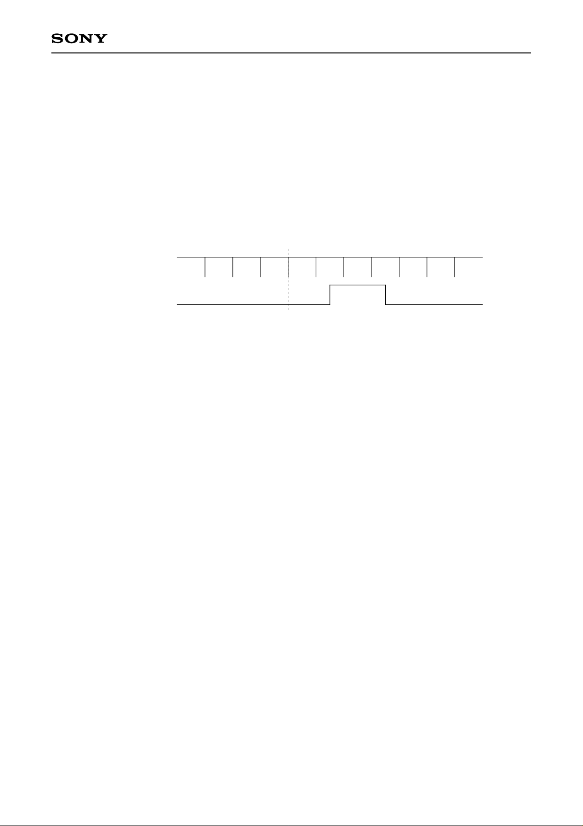
(F) VWA-POSITION
(VM0J, VM1J, VM2J, VM3J, VM4J, VM5J, VM6J, VM7J, VM8J, VM9J, VM0K, VM1K, VM2K, VM3K,
VM4K, VM5K, VM6K, VM7K, VM8K, VM9K)
The VWA pulse rise and fall can be varied in 1H units in the vertical direction.
Rise position: VW0J to 9J (10 bits)
Fall position: VW0K to 9K (10 bits)
Rise, fall transition points: ENB pulse fall position
Reference (0): 1.5H before the VST output position
Reference (0)
Double-speed HSYNC
VST
CXD2443Q
(G) Double-speed setting
(SLBA)
• This bit sets the built-in line double-speed controller.
SLBA
High: Line double-speed controller off
Low: Line double-speed controller on
• The loop counter is an N multiple of the following.
NTSC PAL
910fH 1135fH
Notes on operation
The built-in line double-speed controller is supported only when driving a single LCD panel in NTSC/PAL 4:3
mode. When using the CXD2443Q in other modes (NTSC/PAL 16:9 mode, HD mode, 3-panel mode), be sure
to set the line double-speed controller to off (SLBA = High).
– 22 –
Page 23
CXD2443Q
(H) Double-speed PAL pulse eliminate
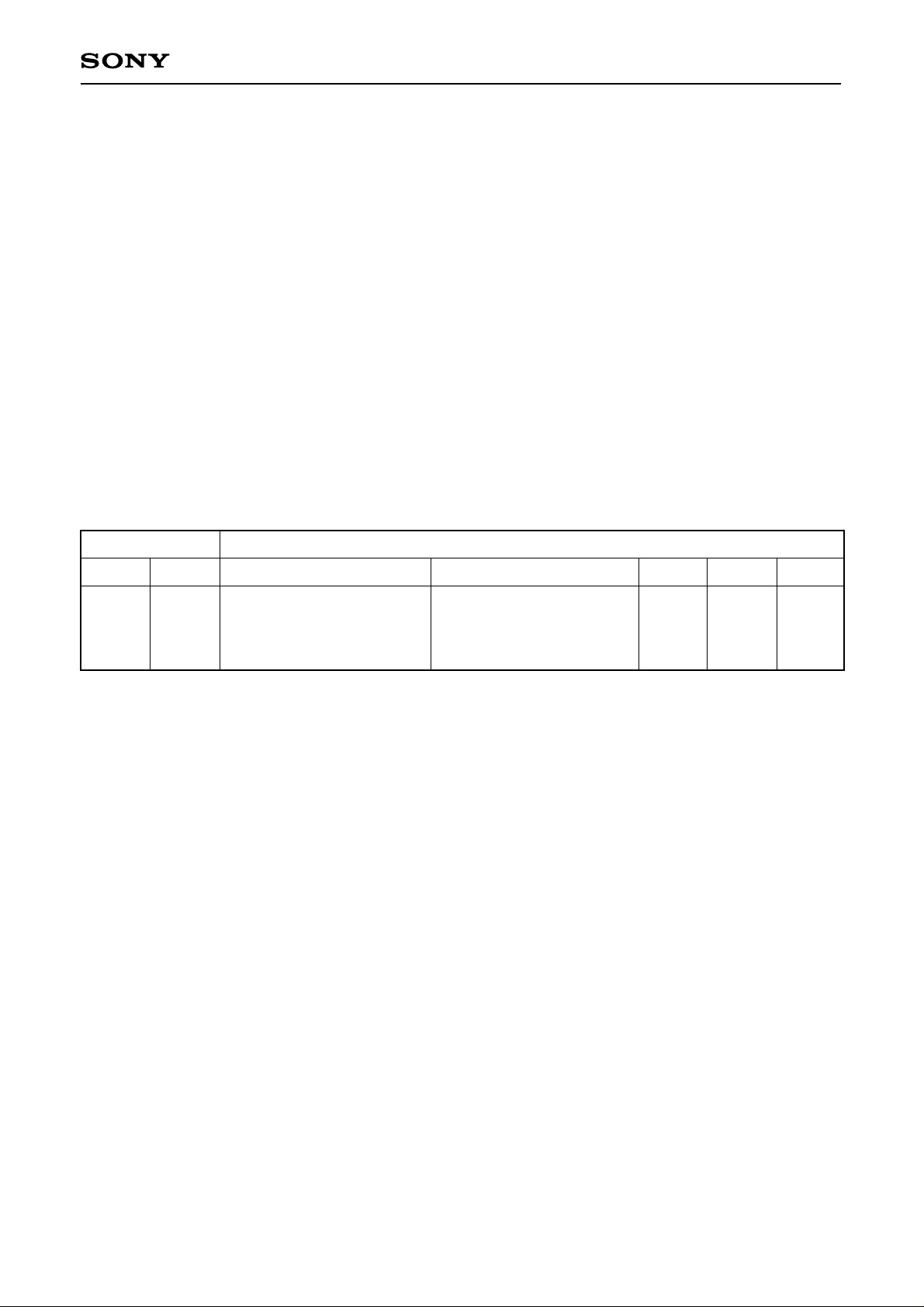
(MA)
This bit sets the double-speed PAL pulse eliminate (conversion from 575 to 480 vertical lines by 6, 7 pulse
eliminate). The setting is as follows.
MA
High: Pulse eliminate off
Low: Pulse eliminate on
The 2N + 1 field pulse eliminate position is shifted 1H (line) to the rear with respect to the 2N field pulse
eliminate position.
(I) Right/left and/or up/down inversion
(RGT, DWN)
These bits switch the right/left inversion and/or up/down inversion timing for the LCD panel.
Output
B outputs
RGT
H
L
H
L
XRGT
L
H
L
H
DWN
H
H
L
L
RGT
H
L
H
L
Setting
DWN
H
H
L
L
A outputs
Right scan, down scan
Left scan, down scan
Right scan, up scan
Left scan, up scan
Left scan, down scan
Right scan, down scan
Left scan, up scan
Right scan, up scan
Note) The B outputs (HSTB, HCKnB, SHnB) are the outputs for 3-panel projectors, and are output at the
right/left inversed timing of the A outputs.
(J) Various settings
SLFR
This bit sets the cycle of the LCD AC drive signals FRP and XFRP.
High: 1H (line) inversion
Low: 1F (field) inversion
VPOL, HPOL
These bits set the input SYNC polarity.
High: Negative polarity
Low: Positive polarity
– 23 –
Page 24

SL3B
This bit sets the 3-panel projector output (B outputs) switching.
The HSTB, HCKnB, and SHnB outputs can be switched on and off.
High: B outputs off
Low: B outputs on
Note) When driving a single LCD panel, set the B outputs to off (SL3B = High).
SLVWB
This bit sets the VWB output.
High: VWB off
Low: VWB on
SLEG
This bit sets the VWB transition timing.
High: HSYNC front edge
Low: HSYNC rear edge
Note) VWB is the equalizing pulse masking pulse.
The rise position is counted from the VD inside the previous field. Therefore, when the number of
lines within one field differs from the standard protocol, the phase between the next field's VSYNC
and the VWB rise position changes.
The phase also changes when a value other than the default value is used as the V-POSITION
setting.
CXD2443Q
(K) Mode settings
SNSL
This bit sets the double-speed HSYNC and standard HSYNC (or CSYNC) input switching.
High: Double-speed HSYNC input
Low: Standard HSYNC (CSYNC) input
Note) When using the built-in line double-speed controller, only the standard HSYNC is supported.
Set SNSL to standard HSYNC input (SNSL = Low).
NT-PAL, XWID, HD
These bits set the various display modes.
NT-PAL XWID XHD
NTSC (4:3) H H H
NTSC (16:9) H L H
PAL (4:3) L H H
PAL (16:9) L L H
HD ∗∗L
Note) Test mode
Serial data TEST1, TEST2, TEST3 and TEST4 are test mode data. Care should be taken as these bits
are not used, and must be set to High.
– 24 –
Page 25

Master Clock 46.07MHz
Loop counter 1464fH
CXD2443Q
H
12f
H
6f
1.2µs (55fH)
2.0µs (92fH)
4.38µs (202fH)
0.55µs (26fH)
0.15µs (7fH)
2.35µs (108fH)
1.2µs (55fH)
0.3µs (14fH)
0.4µs (18fH)
2.1µs (97fH)
1.8µs (83fH)
ODD LINE
1.0µs (46fH)
1444 0 20 40 60 80 100 120 140 160 180 200 220 240 260 280 300 320 340 360 380
HP1, 2, 3, 4, 5, 6, 7, 8: LLLLLLLH SLSH1, 2, 3, 4: LLLL CP1, 2: LH PCGW1, 2: HH RGT: H DWN: H
HPOL: H SLFR: H SNSL: H NT-PL: H XWID: H XHD: H
MCK
HSYNC
XCLP1
HSTA
XCLP2
HCK1A
SH1A
HCK2A
SH2A
SH3A
SH4A
SH5A
SH6A
SH7A
ENB
VCK
FRP
PCG1
PCG2
HDR
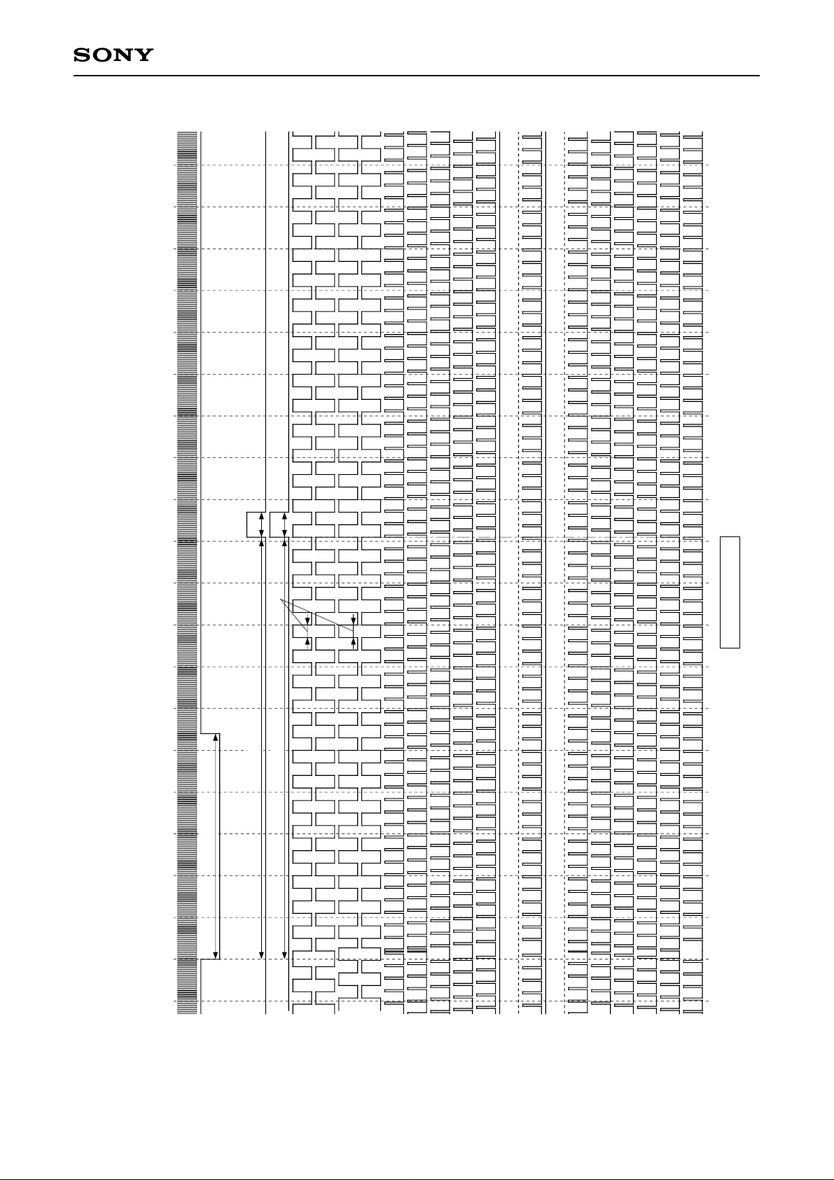
NTSC (4:3) Horizontal Direction Timing Chart
– 25 –
Note) The FRP polarity is not specified for each line and field.
Page 26
CXD2443Q
H
Master Clock 46.07MHz
Loop counter 1464f
3803603403203002802602402202001801601401201008060402001444
12fH
6fH
4.38µs (202fH)
4.38µs (202fH) 12fH
2.35µs (108fH)
ODD LINE
HP1, 2, 3, 4, 5, 6, 7, 8: LLLLLLLH SLSH1, 2, 3, 4: LLLL RGT: H DWN: H
HPOL: H SLFR: H SL3B: L SNSL: H NT-PL: H XWID: H XHD: H
MCK
HSYNC
HSTA
HSTB
HCK1A
HCK2A
HCK1B
HCK2B
SH1A
SH2A
SH3A
SH4A
SH5A
SH6A
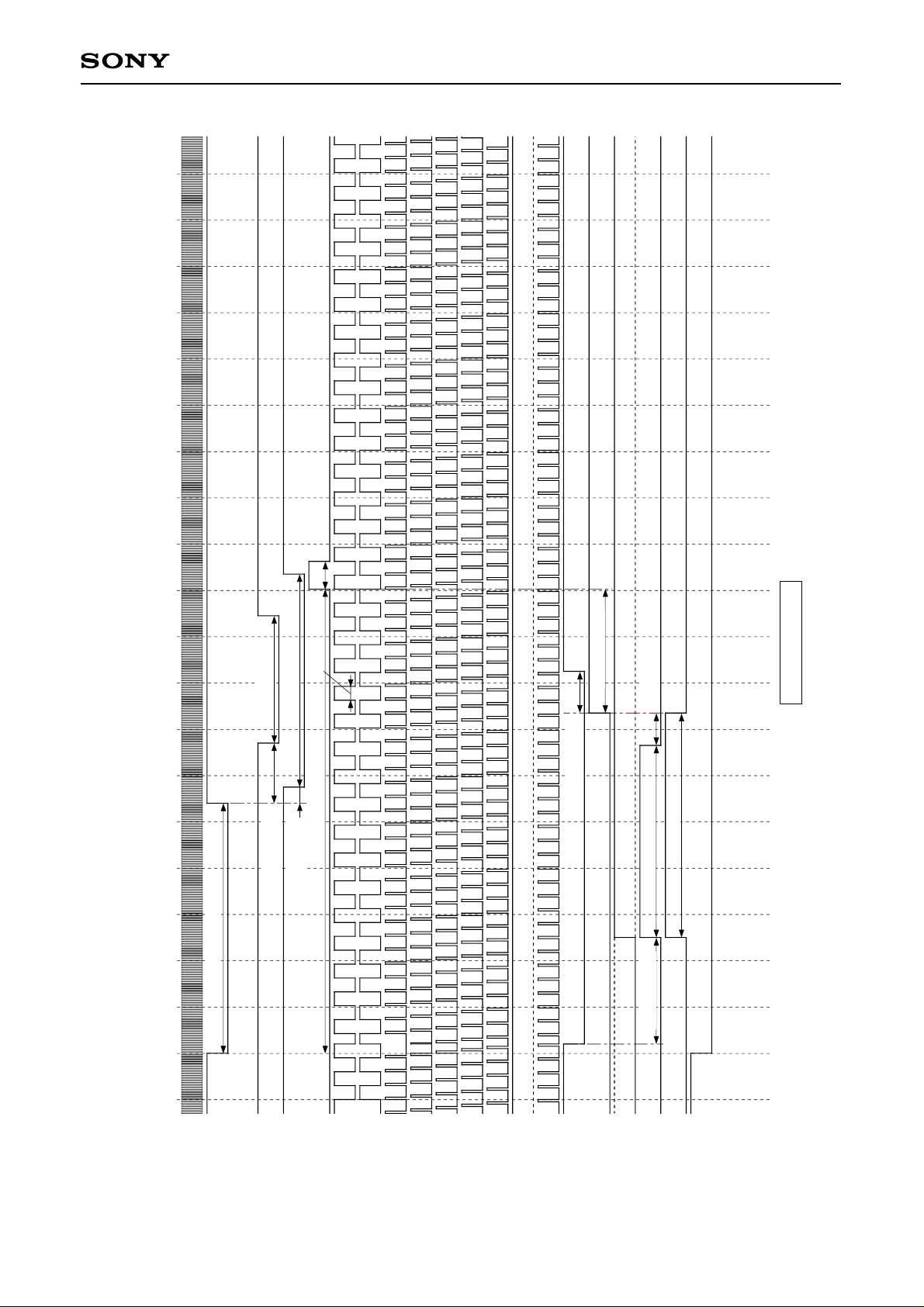
NTSC (4:3) Horizontal Direction Timing Chart (B outputs)
– 26 –
SH7A
SH1B
SH2B
SH3B
SH4B
SH5B
SH6B
SH7B
Page 27
H
Master Clock 46.07MHz
Loop counter 1464f
CXD2443Q
H
12f
6fH
1.16µs (53.5fH)
1.2µs (55fH)
2.0µs (92fH)
0.4µs (18fH)
4.35µs (200.5fH)
0.55µs (26fH)
0.15µs (7fH)
2.35µs (108fH)
0.3µs (14fH)
2.1µs (97fH)
1.8µs (83fH)
EVEN LINE
1.0µs (46fH)
1444 0 20 40 60 80 100 120 140 160 180 200 220 240 260 280 300 320 340 360 380
HP1, 2, 3, 4, 5, 6, 7, 8: LLLLLLLH SLSH1, 2, 3, 4: LLLL CP1, 2: LH PCGW1, 2: HH RGT: H DWN: H
HPOL: H SLFR: H SNSL: H NT-PL: H XWID: H XHD: H
MCK
HSYNC
XCLP1
HSTA
XCLP2
HCK1A
SH1A
HCK2A
SH2A
SH3A
SH4A
SH5A
SH6A
SH7A
ENB
VCK
FRP
PCG1
PCG2
HDR
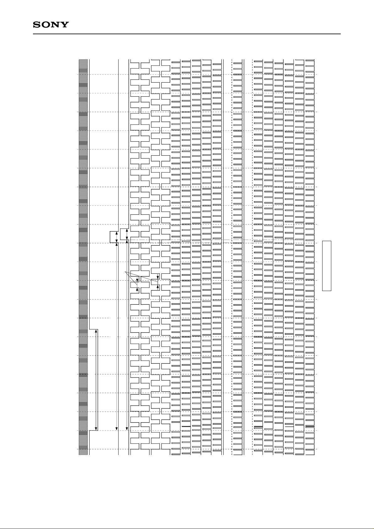
NTSC (4:3) Horizontal Direction Timing Chart
– 27 –
Note) The FRP polarity is not specified for each line and field.
Page 28
Master Clock 46.07MHz
Loop counter 1464fH
CXD2443Q
3803603403203002802602402202001801601401201008060402001444
12fH
12fH
6fH
H)
4.42µs (203.5f
4.35µs (200.5fH)
2.35µs (108fH)
EVEN LINE
HP1, 2, 3, 4, 5, 6, 7, 8: LLLLLLLH SLSH1, 2, 3, 4: LLLL RGT: H DWN: H
HPOL: H SLFR: H SL3B: L SNSL: H NT-PL: H XWID: H XHD: H
MCK
HSYNC
HSTA
HSTB
HCK1A
HCK2A
HCK1B
HCK2B
SH1A
SH2A
SH3A
SH4A
SH5A
SH6A
NTSC (4:3) Horizontal Direction Timing Chart (B outputs)
– 28 –
SH7A
SH1B
SH2B
SH3B
SH4B
SH5B
SH6B
SH7B
Page 29
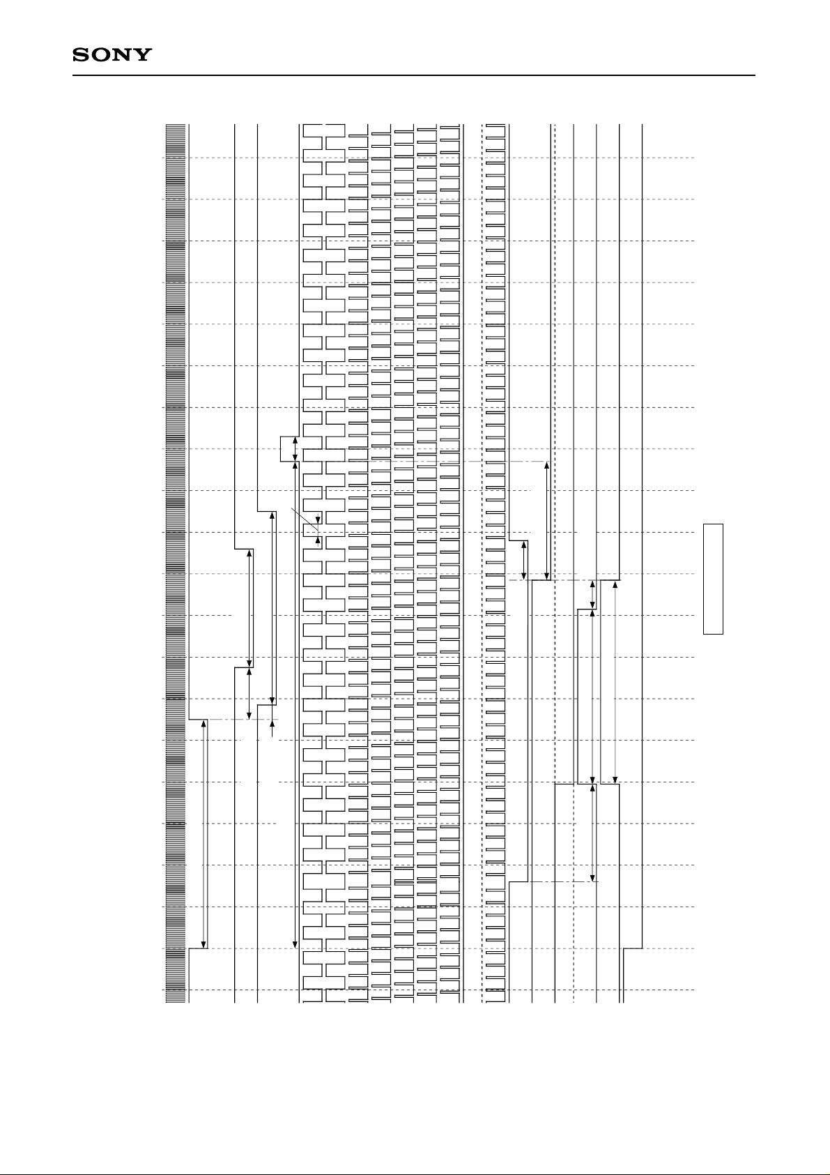
H
Loop counter 1500f
Master Clock 46.88MHz
CXD2443Q
12fH
H
6f
1.2µs (57fH)
0.3µs (14fH)
ODD LINE
1.2µs (57fH)
2.0µs (93fH)
0.55µs (25fH)
0.15µs (7fH)
4.99µs (234fH)
2.35µs (110fH)
0.4µs (19fH)
2.1µs (98fH)
1.8µs (84fH)
1.0µs (47fH)
1480 0 20 40 60 80 100 120 140 160 180 200 220 240 260 280 300 320 340 360 380
HP1, 2, 3, 4, 5, 6, 7, 8: LLLLLLLH SLSH1, 2, 3, 4: LLLL CP1, 2: LH PCGW1, 2: HH RGT: H DWN: H
HPOL: H SLFR: H SNSL: H NT-PL: L XWID: H XHD: H
MCK
HSYNC
XCLP1
HSTA
XCLP2
HCK1A
SH1A
HCK2A
SH2A
SH3A
SH4A
SH5A
SH6A
SH7A
ENB
VCK
FRP
PCG1
PCG2
HDR
PAL (4:3) Horizontal Direction Timing Chart
– 29 –
Note) The FRP polarity is not specified for each line and field.
Page 30
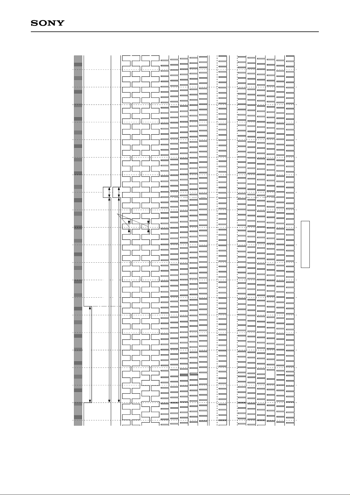
3803603403203002802602402202001801601401201008060402001480
Loop counter 1500fHMaster Clock 46.88MHz
CXD2443Q
12fH
12fH
6fH
ODD LINE
H)
4.99µs (234f
4.99µs (234fH)
2.35µs (110fH)
HP1, 2, 3, 4, 5, 6, 7, 8: LLLLLLLH SLSH1, 2, 3, 4: LLLL RGT: H DWN: H
HPOL: H SLFR: H SL3B: L SNSL: H NT-PL: L XWID: H XHD: H
MCK
HSYNC
HSTA
HSTB
HCK1A
HCK2A
HCK1B
HCK2B
SH1A
SH2A
SH3A
SH4A
SH5A
SH6A
PAL (4:3) Horizontal Direction Timing Chart (B outputs)
– 30 –
SH7A
SH1B
SH2B
SH3B
SH4B
SH5B
SH6B
SH7B
Page 31
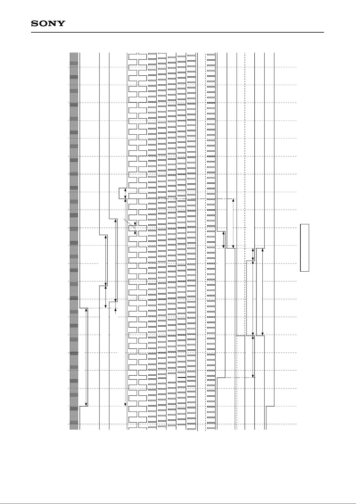
H
Master Clock 46.88MHz
Loop counter 1500f
CXD2443Q
12fH
H
6f
1.18µs (55.5fH)
0.3µs (14fH)
EVEN LINE
1.2µs (57fH)
2.0µs (93fH)
0.55µs (25fH)
0.15µs (7fH)
2.35µs (110fH)
4.96µs (232.5fH)
0.4µs (19fH)
2.1µs (98fH)
1.8µs (84fH)
1.0µs (47fH)
1480 0 20 40 60 80 100 120 140 160 180 200 220 240 260 280 300 320 340 360 380
HP1, 2, 3, 4, 5, 6, 7, 8: LLLLLLLH SLSH1, 2, 3, 4: LLLL CP1, 2: LH PCGW1, 2: HH RGT: H DWN: H
HPOL: H SLFR: H SNSL: H NT-PL: L XWID: H XHD: H
MCK
HSYNC
XCLP1
HSTA
XCLP2
HCK1A
SH1A
HCK2A
SH2A
SH3A
SH4A
SH5A
SH6A
SH7A
ENB
VCK
FRP
PCG1
PCG2
HDR
PAL (4:3) Horizontal Direction Timing Chart
– 31 –
Note) The FRP polarity is not specified for each line and field.
Page 32
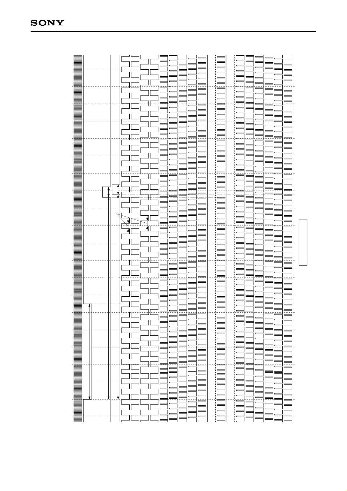
CXD2443Q
H
Loop counter 1500f
Master Clock 46.88MHz
3803603403203002802602402202001801601401201008060402001480
12fH
12fH
6fH
EVEN LINE
H)
5.02µs (235.5f
4.96µs (232.5fH)
2.35µs (110fH)
HP1, 2, 3, 4, 5, 6, 7, 8: LLLLLLLH SLSH1, 2, 3, 4: LLLL RGT: H DWN: H
HPOL: H SLFR: H SL3B: L SNSL: H NT-PL: L XWID: H XHD: H
MCK
HSYNC
HSTA
HSTB
HCK1A
HCK2A
HCK1B
HCK2B
SH1A
SH2A
SH3A
SH4A
SH5A
SH6A
PAL (4:3) Horizontal Direction Timing Chart (B outputs)
– 32 –
SH7A
SH1B
SH2B
SH3B
SH4B
SH5B
SH6B
SH7B
Page 33
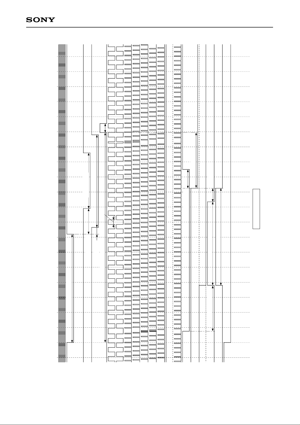
H
Loop counter 1952f
Master Clock 61.43MHz
CXD2443Q
12fH
1.2µs (74fH)
2.0µs (123fH)
1.2µs (74fH)
0.4µs (25fH)
6fH
0.55µs (34fH)
0.15µs (9fH)
4.54µs (279fH)
2.35µs (144fH)
0.3µs (18fH)
ODD LINE
2.1µs (129fH)
1.8µs (111fH)
1.0µs (61fH)
1932 0 20 40 60 80 100 120 140 160 180 200 220 240 260 280 300 320 340 360 380
HP1, 2, 3, 4, 5, 6, 7, 8: LLLLLLLH SLSH1, 2, 3, 4: LLLL CP1, 2: LH PCGW1, 2: HH RGT: H DWN: H
HPOL: H SLFR: H SNSL: H NT-PL: H XWID: L XHD: H
MCK
HSYNC
XCLP1
HSTA
XCLP2
HCK1A
SH1A
HCK2A
SH2A
SH3A
SH4A
SH5A
SH6A
SH7A
ENB
VCK
FRP
PCG1
PCG2
HDR
NTSC (16:9) Horizontal Direction Timing Chart
– 33 –
Note) The FRP polarity is not specified for each line and field.
Page 34
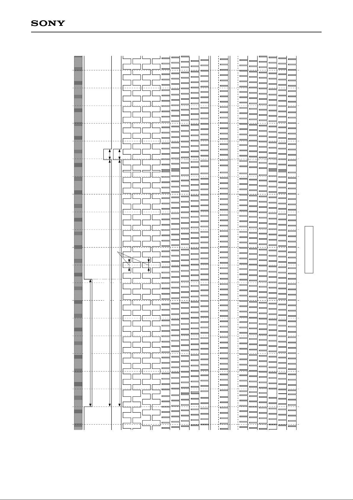
Master Clock 61.43MHz
Loop counter 1952fH
3803603403203002802602402202001801601401201008060402001932
CXD2443Q
12fH
12fH
6fH
H)
4.54µs (279f
4.54µs (279fH)
2.35µs (144fH)
ODD LINE
HP1, 2, 3, 4, 5, 6, 7, 8: LLLLLLLH SLSH1, 2, 3, 4: LLLL RGT: H DWN: H
HPOL: H SLFR: H SL3B: L SNSL: H NT-PL: H XWID: L XHD: H
MCK
HSYNC
HSTA
HSTB
HCK1A
HCK2A
HCK1B
HCK2B
SH1A
SH2A
SH3A
SH4A
SH5A
SH6A
NTSC (16:9) Horizontal Direction Timing Chart (B outputs)
– 34 –
SH7A
SH1B
SH2B
SH3B
SH4B
SH5B
SH6B
SH7B
Page 35
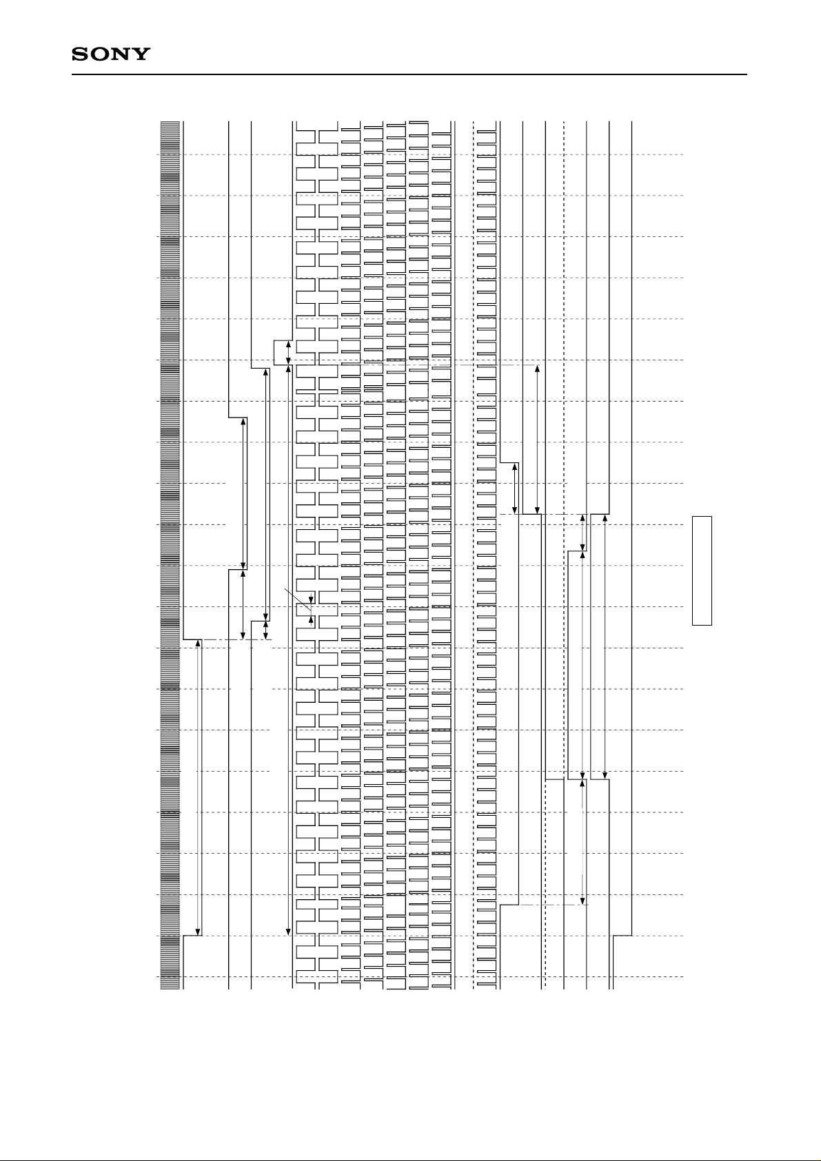
H
Master Clock 61.43MHz
Loop counter 1952f
CXD2443Q
12fH
1.18µs (72.5fH)
1.2µs (74fH)
2.0µs (123fH)
H
6f
0.15µs (9fH)
0.55µs (34fH)
4.52µs (277.5fH)
2.35µs (144fH)
0.4µs (25fH)
0.3µs (18fH)
EVEN LINE
2.1µs (129fH)
1.8µs (111fH)
1.0µs (61fH)
1932 0 20 40 60 80 100 120 140 160 180 200 220 240 260 280 300 320 340 360 380
HP1, 2, 3, 4, 5, 6, 7, 8: LLLLLLLH SLSH1, 2, 3, 4: LLLL CP1, 2: LH PCGW1, 2: HH RGT: H DWN: H
HPOL: H SLFR: H SNSL: H NT-PL: H XWID: L XHD: H
MCK
HSYNC
XCLP1
HSTA
XCLP2
HCK1A
SH1A
HCK2A
SH2A
SH3A
SH4A
SH5A
SH6A
SH7A
ENB
VCK
FRP
PCG1
PCG2
HDR
NTSC (16:9) Horizontal Direction Timing Chart
– 35 –
Note) The FRP polarity is not specified for each line and field.
Page 36
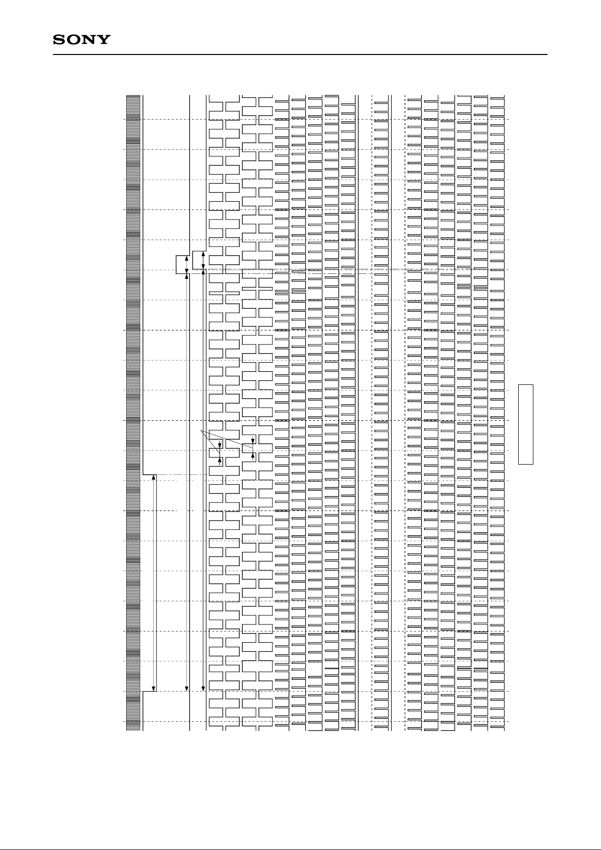
3803603403203002802602402202001801601401201008060402001932
Loop counter 1952fHMaster Clock 61.43MHz
CXD2443Q
12fH
12fH
6fH
H)
4.52µs (277.5fH)
4.57µs (280.5f
2.35µs (144fH)
EVEN LINE
HP1, 2, 3, 4, 5, 6, 7, 8: LLLLLLLH SLSH1, 2, 3, 4: LLLL RGT: H DWN: H
HPOL: H SLFR: H SL3B: L SNSL: H NT-PL: H XWID: L XHD: H
MCK
HSYNC
HSTA
HSTB
HCK1A
HCK2A
HCK1B
HCK2B
SH1A
SH2A
SH3A
SH4A
SH5A
SH6A
NTSC (16:9) Horizontal Direction Timing Chart (B outputs)
– 36 –
SH7A
SH1B
SH2B
SH3B
SH4B
SH5B
SH6B
SH7B
Page 37
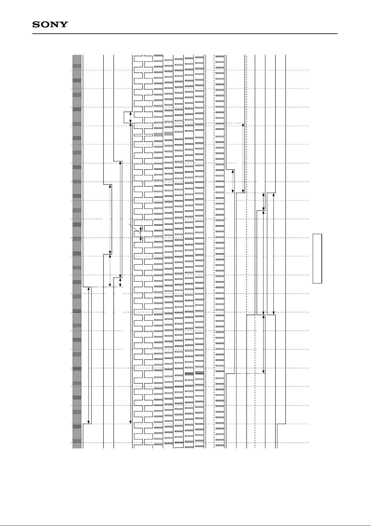
H
Loop counter 2000f
Master Clock 62.5MHz
CXD2443Q
H
12f
1.2µs (75fH)
0.3µs (19fH)
6fH
2.0µs (125fH)
1.2µs (75fH)
0.55µs (35fH)
0.15µs (10fH)
5.17µs (323fH)
2.35µs (147fH)
0.4µs (25fH)
1.8µs (112fH)
2.1µs (131fH)
1.0µs (63fH)
ODD LINE
1980 0 20 40 60 80 100 120 140 160 180 200 220 240 260 280 300 320 340 360 380
HP1, 2, 3, 4, 5, 6, 7, 8: LLLLLLLH SLSH1, 2, 3, 4: LLLL CP1, 2: LH PCGW1, 2: HH RGT: H DWN: H
HPOL: H SLFR: H SNSL: H NT-PL: L XWID: L XHD: H
MCK
HSYNC
XCLP1
HSTA
XCLP2
HCK1A
SH1A
HCK2A
SH2A
SH3A
SH4A
SH5A
SH6A
SH7A
ENB
VCK
FRP
PCG1
PCG2
HDR
PAL (16:9) Horizontal Direction Timing Chart
– 37 –
Note) The FRP polarity is not specified for each line and field.
Page 38

CXD2443Q
H
Loop counter 2000f
Master Clock 62.5MHz
3803603403203002802602402202001801601401201008060402001980
12fH
12fH
H
6f
H)
ODD LINE
5.17µs (323f
5.17µs (323fH)
2.35µs (147fH)
HP1, 2, 3, 4, 5, 6, 7, 8: LLLLLLLH SLSH1, 2, 3, 4: LLLL RGT: H DWN: H
HPOL: H SLFR: H SL3B: L SNSL: H NT-PL: L XWID: L XHD: H
MCK
HSYNC
HSTA
HSTB
HCK1A
HCK2A
HCK1B
HCK2B
SH1A
SH2A
SH3A
SH4A
SH5A
SH6A
PAL (16:9) Horizontal Direction Timing Chart (B outputs)
– 38 –
SH7A
SH1B
SH2B
SH3B
SH4B
SH5B
SH6B
SH7B
Page 39
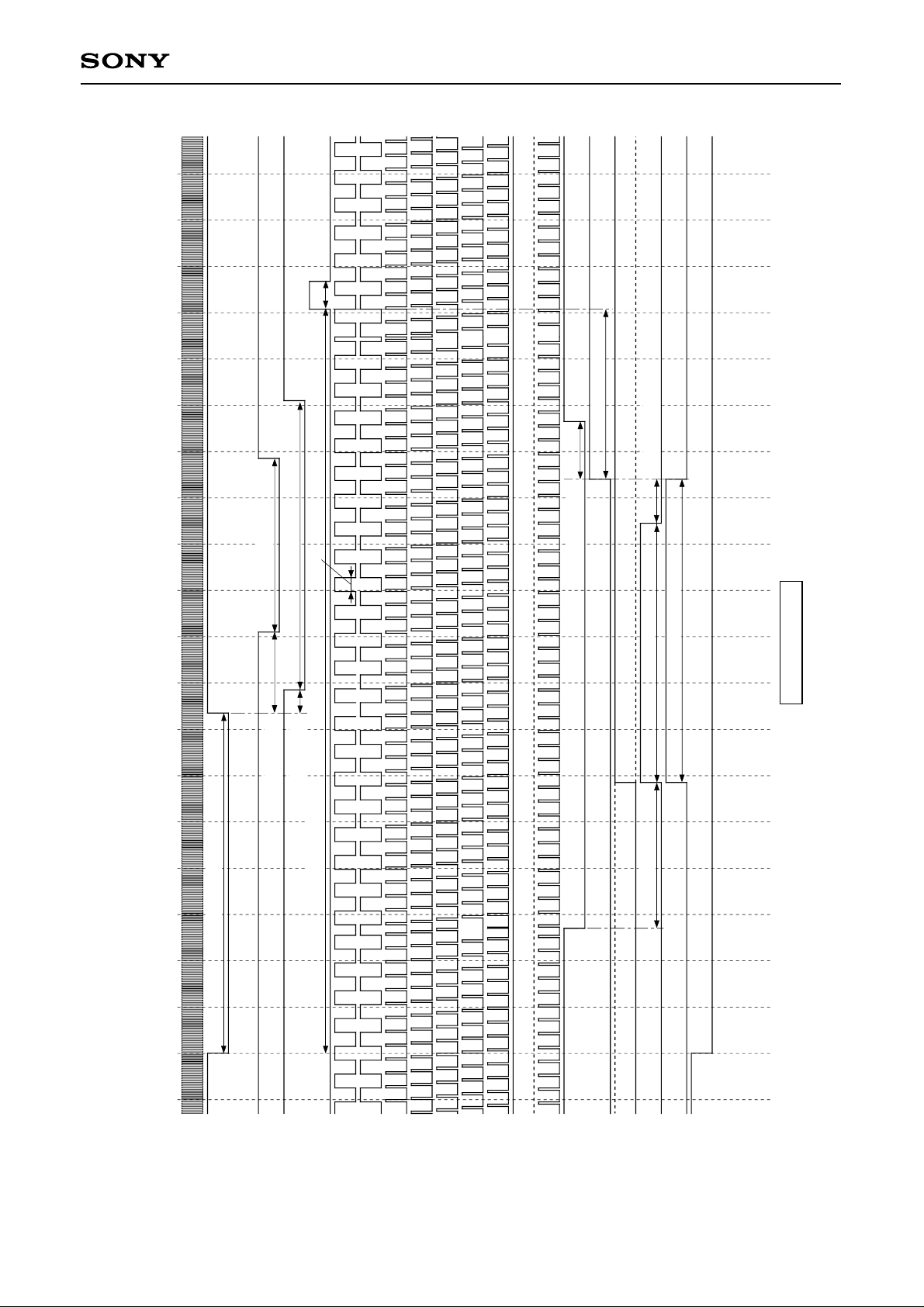
Master Clock 62.5MHz
Loop counter 2000fH
CXD2443Q
H
12f
1.18µs (73.5fH)
0.3µs (19fH)
0.4µs (25fH)
6fH
2.0µs (125fH)
1.2µs (75fH)
2.1µs (131fH)
1.8µs (112fH)
0.15µs (10fH)
0.55µs (35fH)
5.14µs (321.5fH)
1.0µs (63fH)
2.35µs (147fH)
EVEN LINE
1980 0 20 40 60 80 100 120 140 160 180 200 220 240 260 280 300 320 340 360 380
HP1, 2, 3, 4, 5, 6, 7, 8: LLLLLLLH SLSH1, 2, 3, 4: LLLL CP1, 2: LH PCGW1, 2: HH RGT: H DWN: H
HPOL: H SLFR: H SNSL: H NT-PL: L XWID: L XHD: H
MCK
HSYNC
XCLP1
HSTA
XCLP2
HCK1A
SH1A
HCK2A
SH2A
SH3A
SH4A
SH5A
SH6A
SH7A
ENB
VCK
FRP
PCG1
PCG2
HDR
PAL (16:9) Horizontal Direction Timing Chart
– 39 –
Note) The FRP polarity is not specified for each line and field.
Page 40
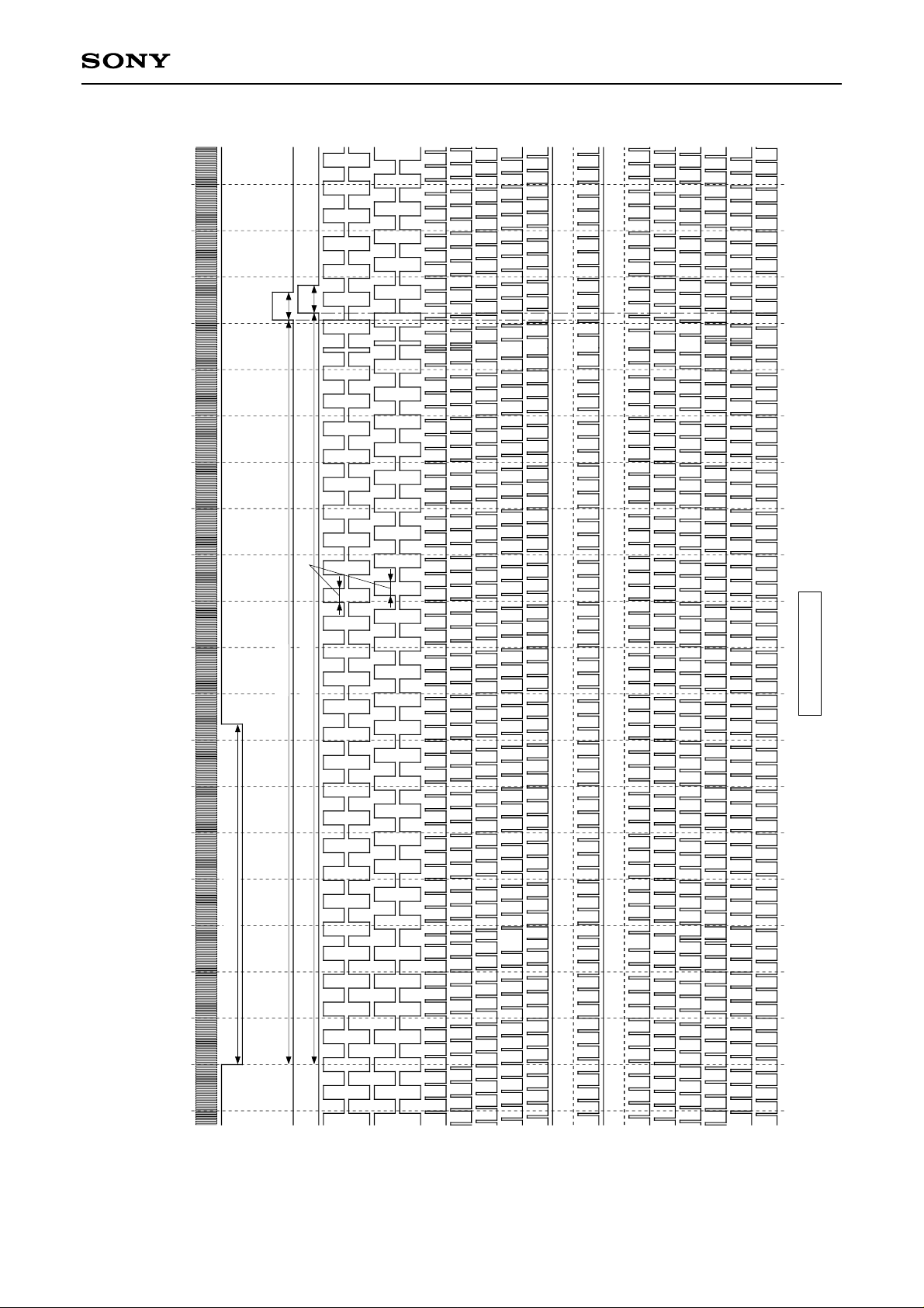
CXD2443Q
H
Loop counter 2000f
Master Clock 62.5MHz
3803603403203002802602402202001801601401201008060402001980
12fH
12fH
6fH
H)
H)
EVEN LINE
5.19µs (324.5f
5.14µs (321.5f
2.35µs (147fH)
HP1, 2, 3, 4, 5, 6, 7, 8: LLLLLLLH SLSH1, 2, 3, 4: LLLL RGT: H DWN: H
HPOL: H SLFR: H SL3B: L SNSL: H NT-PL: L XWID: L XHD: H
MCK
HSYNC
HSTA
HSTB
HCK1A
HCK2A
HCK1B
HCK2B
SH1A
SH2A
SH3A
SH4A
SH5A
SH6A
PAL (16:9) Horizontal Direction Timing Chart (B outputs)
– 40 –
SH7A
SH1B
SH2B
SH3B
SH4B
SH5B
SH6B
SH7B
Page 41
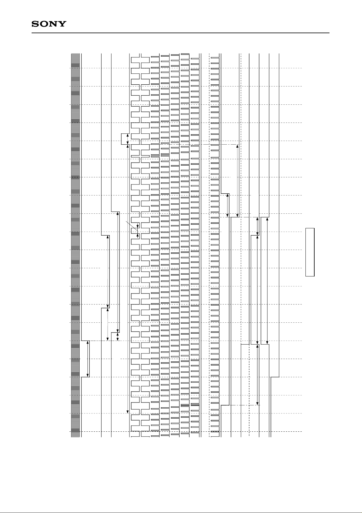
H
Loop counter 1976f
Master Clock 66.69MHz
CXD2443Q
12fH
1.2µs (80fH)
0.3µs (20fH)
6fH
0.4µs (26fH)
ODD LINE
1.2µs (80fH)
2.0µs (133fH)
2.1µs (140fH)
1.8µs (120fH)
3.84µs (256fH)
0.55µs (36fH)
0.59µs (40fH)
0.15µs (9fH)
1.0µs (67fH)
1936 1956
1916 0 20 40 60 80 100 120 140 160 180 200 220 240 260 280 300 320 340
HP1, 2, 3, 4, 5, 6, 7, 8: LLLLLLLH SLSH1, 2, 3, 4: LLLL CP1, 2: LH PCGW1, 2: HH RGT: H DWN: H
HPOL: H SLFR: H XHD: L
MCK
HSYNC
XCLP1
HSTA
XCLP2
HCK1A
SH1A
HCK2A
SH2A
SH3A
SH4A
SH5A
SH6A
SH7A
ENB
VCK
FRP
PCG1
PCG2
HDR
HD Horizontal Direction Timing Chart
– 41 –
Note) The FRP polarity is not specified for each line and field.
Page 42

CXD2443Q
H
Master Clock 66.69MHz
Loop counter 1976f
3406020 32030028026024022020018016014012010080400195619361916
12fH
12fH
6fH
ODD LINE
3.84µs (256fH)
3.84µs (256fH)
0.59µs (40fH)
HP1, 2, 3, 4, 5, 6, 7, 8: LLLLLLLH SLSH1, 2, 3, 4: LLLL RGT: H DWN: H
HPOL: H SLFR: H SL3B: L XHD: L
MCK
HSYNC
HSTA
HSTB
HCK1A
HCK2A
HCK1B
HCK2B
SH1A
SH2A
SH3A
SH4A
SH5A
SH6A
HD Horizontal Direction Timing Chart (B outputs)
– 42 –
SH7A
SH1B
SH2B
SH3B
SH4B
SH5B
SH6B
SH7B
Page 43

H
Loop counter 1976f
Master Clock 66.69MHz
CXD2443Q
12fH
1.18µs (78.5fH)
0.3µs (20fH)
6fH
0.4µs (26fH)
EVEN LINE
1.2µs (80fH)
2.0µs (133fH)
2.1µs (140fH)
1.8µs (120fH)
3.82µs (254.5fH)
0.55µs (36fH)
0.59µs (40fH)
0.15µs (9fH)
1.0µs (67fH)
1936 1956
1916 0 20 40 60 80 100 120 140 160 180 200 220 240 260 280 300 320 340
HP1, 2, 3, 4, 5, 6, 7, 8: LLLLLLLH SLSH1, 2, 3, 4: LLLL CP1, 2: LH PCGW1, 2: HH RGT: H DWN: H
HPOL: H SLFR: H XHD: L
MCK
HSYNC
XCLP1
HSTA
XCLP2
HCK1A
SH1A
HCK2A
SH2A
SH3A
SH4A
SH5A
SH6A
SH7A
ENB
VCK
FRP
PCG1
PCG2
HDR
HD Horizontal Direction Timing Chart
– 43 –
Note) The FRP polarity is not specified for each line and field.
Page 44
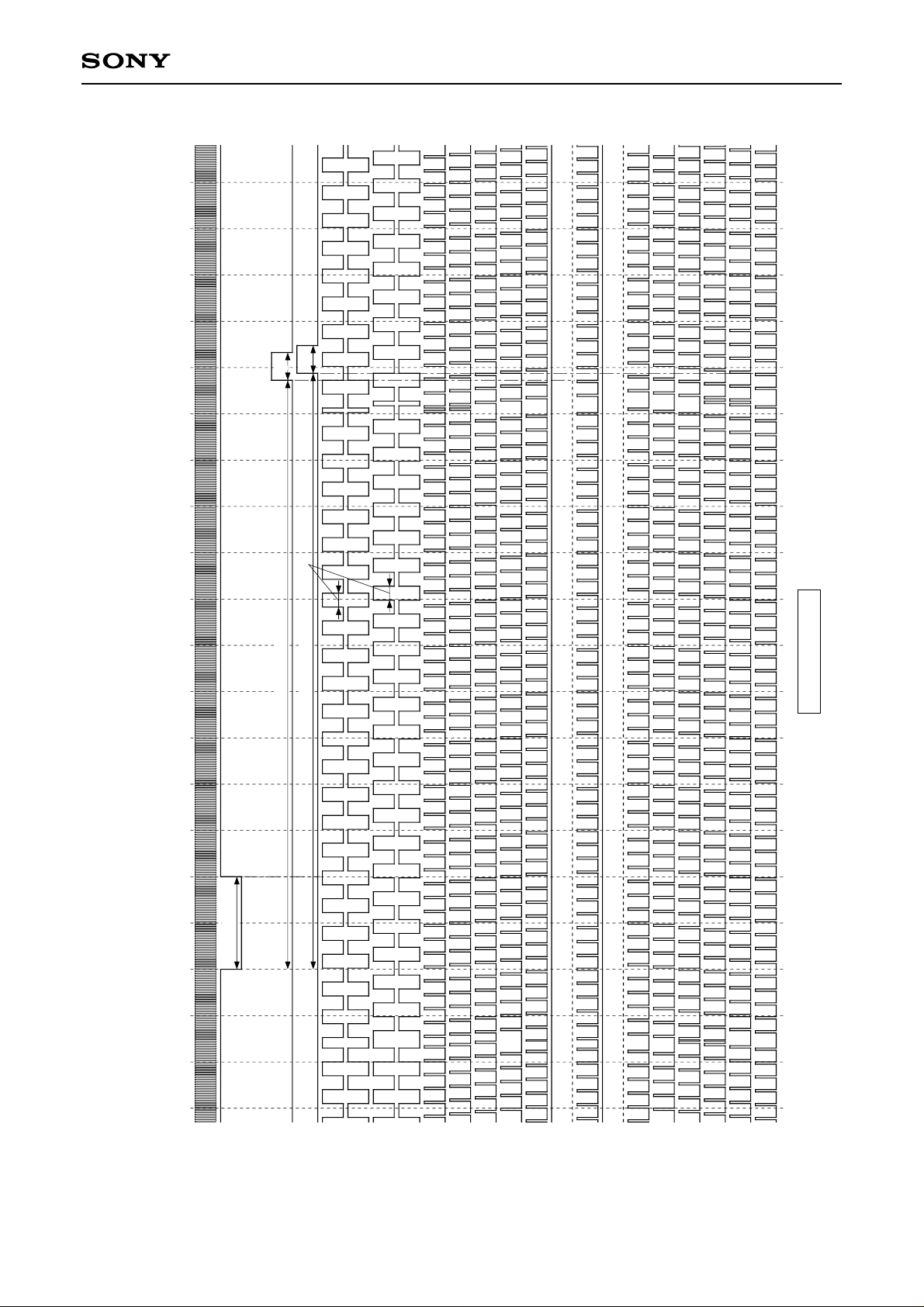
CXD2443Q
H
Master Clock 66.69MHz
Loop counter 1976f
3406020 32030028026024022020018016014012010080400195619361916
12fH
12fH
6fH
H)
EVEN LINE
3.86µs (257.5f
3.82µs (254.5fH)
0.59µs (40fH)
HP1, 2, 3, 4, 5, 6, 7, 8: LLLLLLLH SLSH1, 2, 3, 4: LLLL RGT: H DWN: H
HPOL: H SLFR: H SL3B: L XHD: L
MCK
HSYNC
HSTA
HSTB
HCK1A
HCK2A
HCK1B
HCK2B
SH1A
SH2A
SH3A
SH4A
SH5A
SH6A
HD Horizontal Direction Timing Chart (B outputs)
– 44 –
SH7A
SH1B
SH2B
SH3B
SH4B
SH5B
SH6B
SH7B
Page 45
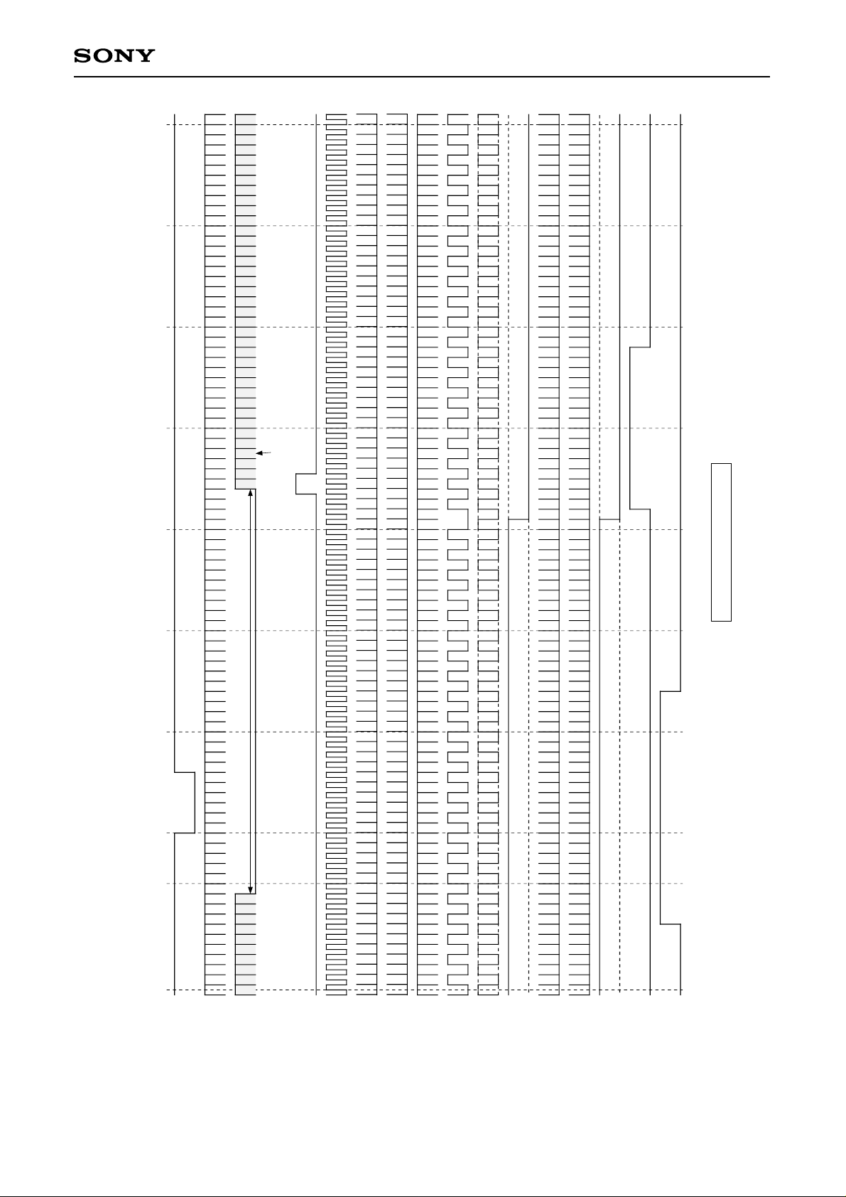
700 605040302010520510
CXD2443Q
123456789101112
21H
Display start
Double-speed HSYNC input
484
483 485
Note) The FRP polarity is not specified for each line and field.
(BLK) in the timing chart is a pulse indicated as a reference and is not a pulse output from pins.
VD
VP1, 2, 3, 4: LLLH VM0J, 1J, 2J, 3J, 4J, 5J, 6J, 7J, 8J, 9J: LLLLLLLLL VM0J, 1J, 2J, 3J, 4J, 5J, 6J, 7J, 8J, 9J: LLLLHLLLL
MA: H SL3B: L VPOL: H SNSL: H NT-PL: H XHD: H
HSYNC
(BLK)
NTSC (double-speed HSYNC input) Vertical Direction Timing Chart
VST
HDR
HSTA
HSTB
ENB
VCK
FRP (1H inversed)
PCG1
PCG2
FRP (1F inversed)
FLDO
VWA
VWB
– 45 –
Page 46
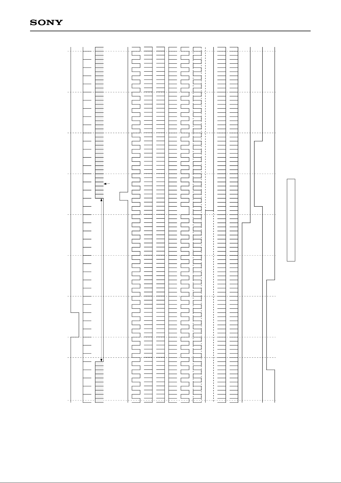
700 605040302010520510
CXD2443Q
123456789101112
21H
Display start
ODD FIELD (standard HSYNC input)
484
483 485
Note) The FRP polarity is not specified for each line and field.
(BLK) in the timing chart is a pulse indicated as a reference and is not a pulse output from pins.
VD
VP1, 2, 3, 4: LLLH VM0J, 1J, 2J, 3J, 4J, 5J, 6J, 7J, 8J, 9J: LLLLLLLLL VM0J, 1J, 2J, 3J, 4J, 5J, 6J, 7J, 8J, 9J: LLLLHLLLL
MA: H SL3B: L VPOL: H SNSL: L NT-PL: H XHD: H
HSYNC
(BLK)
NTSC (standard HSYNC input) Vertical Direction Timing Chart
VST
HDR
HSTA
HSTB
ENB
VCK
FRP (1H inversed)
PCG1
PCG2
FRP (1F inversed)
FLDO
VWA
VWB
– 46 –
Page 47

700 605040302010520510
CXD2443Q
123456789101112
21H
Display start
EVEN FIELD (standard HSYNC input)
484
483 485
Note) The FRP polarity is not specified for each line and field.
(BLK) in the timing chart is a pulse indicated as a reference and is not a pulse output from pins.
VD
VP1, 2, 3, 4: LLLH VM0J, 1J, 2J, 3J, 4J, 5J, 6J, 7J, 8J, 9J: LLLLLLLLL VM0J, 1J, 2J, 3J, 4J, 5J, 6J, 7J, 8J, 9J: LLLLHLLLL
MA: H SL3B: L VPOL: H SNSL: L NT-PL: H XHD: H
HSYNC
(BLK)
NTSC (standard HSYNC input) Vertical Direction Timing Chart
VST
HDR
HSTA
HSTB
ENB
VCK
FRP (1H inversed)
PCG1
PCG2
FRP (1F inversed)
FLDO
VWA
VWB
– 47 –
Page 48
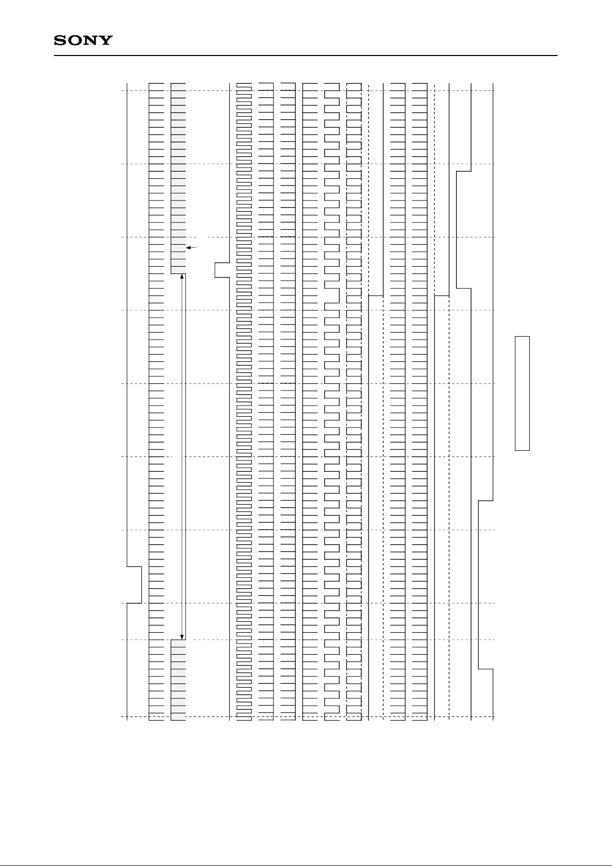
700 605040302010620610
123456789101112
CXD2443Q
Display start
25H
600
598
599
Double-speed HSYNC input
Note) The FRP polarity is not specified for each line and field.
(BLK) in the timing chart is a pulse indicated as a reference and is not a pulse output from pins.
VD
VP1, 2, 3, 4: LLLH VM0J, 1J, 2J, 3J, 4J, 5J, 6J, 7J, 8J, 9J: LLLLLLLLL VM0J, 1J, 2J, 3J, 4J, 5J, 6J, 7J, 8J, 9J: LLLLHLLLL
MA: H SL3B: L VPOL: H SNSL: H NT-PL: L XHD: H
HSYNC
(BLK)
PAL (double-speed HSYNC input) Vertical Direction Timing Chart
VST
HDR
HSTA
HSTB
ENB
VCK
FRP (1H inversed)
PCG1
PCG2
FRP (1F inversed)
FLDO
VWA
VWB
– 48 –
Page 49
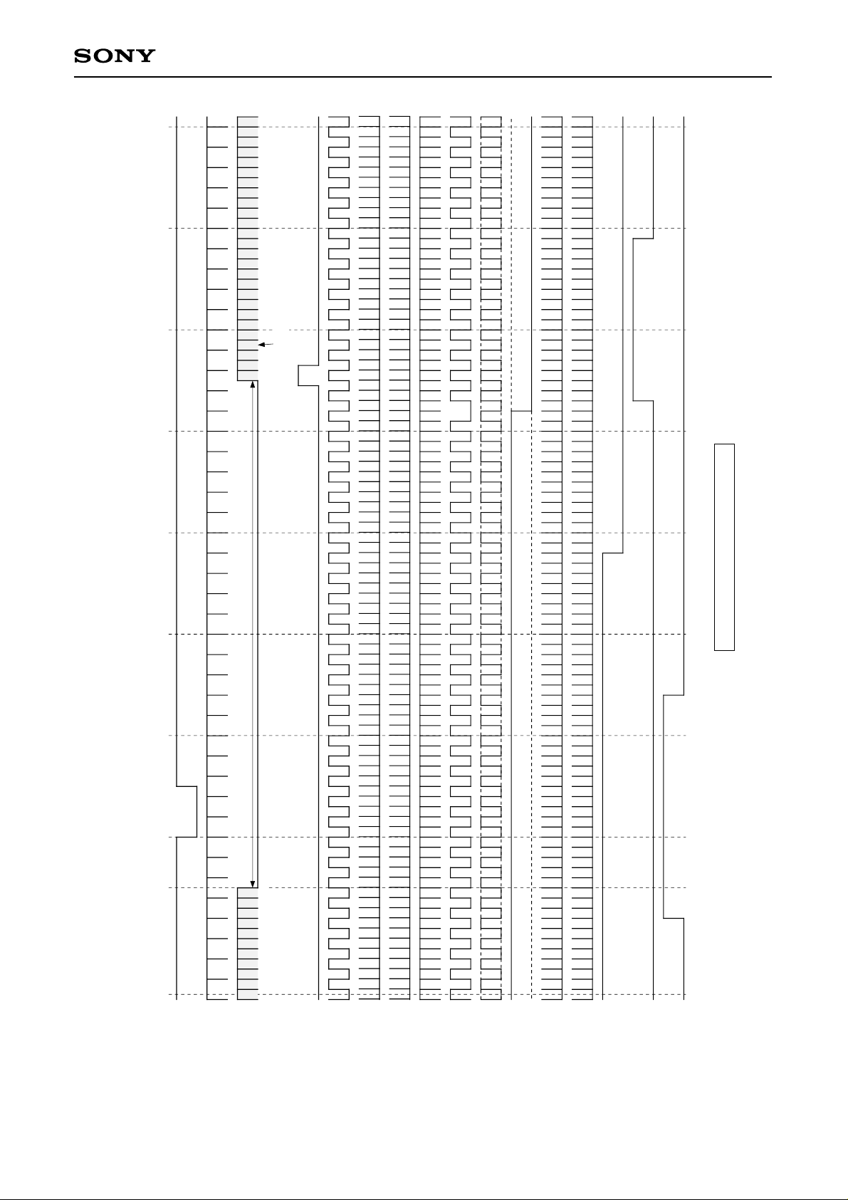
700 605040302010620610
CXD2443Q
123456789101112
Display start
25H
600
598
599
ODD FIELD (standard HSYNC input)
Note) The FRP polarity is not specified for each line and field.
(BLK) in the timing chart is a pulse indicated as a reference and is not a pulse output from pins.
VD
VP1, 2, 3, 4: LLLH VM0J, 1J, 2J, 3J, 4J, 5J, 6J, 7J, 8J, 9J: LLLLLLLLL VM0J, 1J, 2J, 3J, 4J, 5J, 6J, 7J, 8J, 9J: LLLLHLLLL
MA: H SL3B: L VPOL: H SNSL: L NT-PL: L XHD: H
HSYNC
(BLK)
PAL (standard HSYNC input) Vertical Direction Timing Chart
VST
HDR
HSTA
HSTB
ENB
VCK
FRP (1H inversed)
PCG1
PCG2
FRP (1F inversed)
FLDO
VWA
VWB
– 49 –
Page 50
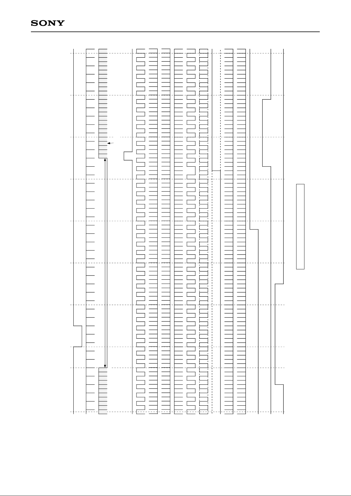
700 605040302010620610
123456789101112
CXD2443Q
Display start
25H
600
598
599
EVEN FIELD (standard HSYNC input)
Note) The FRP polarity is not specified for each line and field.
(BLK) in the timing chart is a pulse indicated as a reference and is not a pulse output from pins.
VD
VP1, 2, 3, 4: LLLH VM0J, 1J, 2J, 3J, 4J, 5J, 6J, 7J, 8J, 9J: LLLLLLLLL VM0J, 1J, 2J, 3J, 4J, 5J, 6J, 7J, 8J, 9J: LLLLHLLLL
MA: H SL3B: L VPOL: H SNSL: L NT-PL: L XHD: H
HSYNC
(BLK)
PAL (standard HSYNC input) Vertical Direction Timing Chart
VST
HDR
HSTA
HSTB
ENB
VCK
FRP (1H inversed)
PCG1
PCG2
FRP (1F inversed)
FLDO
VWA
VWB
– 50 –
Page 51
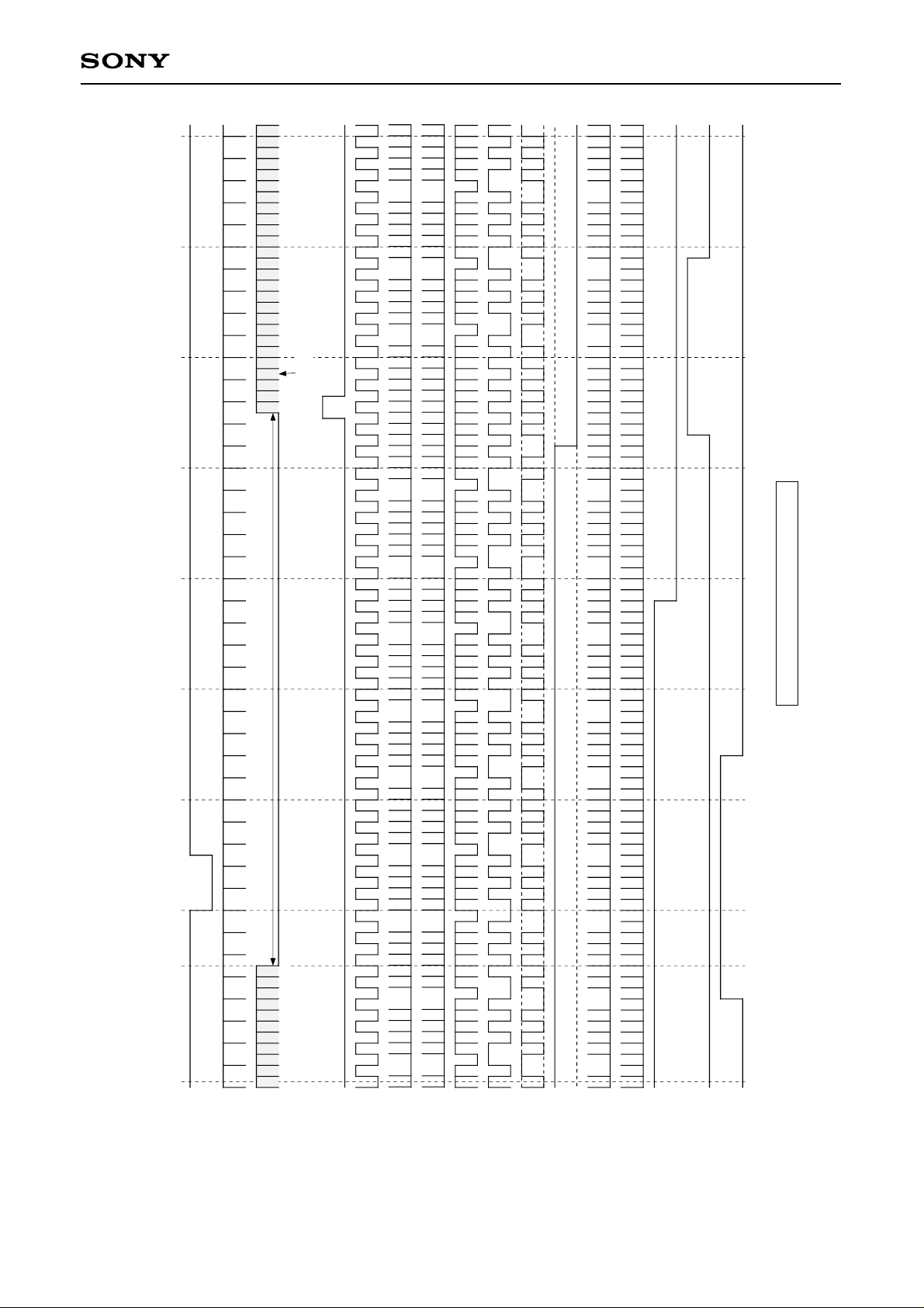
700 605040302010620610
1 2 3 4 5 6 7 8 9 10 1112
CXD2443Q
Display start
25H
600
598
599
ODD FIELD (standard HSYNC input)
Note) The FRP polarity is not specified for each line and field.
(BLK) in the timing chart is a pulse indicated as a reference and is not a pulse output from pins.
VD
VP1, 2, 3, 4: LLLH VM0J, 1J, 2J, 3J, 4J, 5J, 6J, 7J, 8J, 9J: LLLLLLLLL VM0J, 1J, 2J, 3J, 4J, 5J, 6J, 7J, 8J, 9J: LLLLHLLLL
MA: L SL3B: L VPOL: H SNSL: L NT-PL: L XHD: H
HSYNC
(BLK)
PAL (pulse eliminate display, standard HSYNC input) Vertical Direction Timing Chart
VST
HDR
HSTA
HSTB
ENB
VCK
FRP (1H inversed)
PCG1
PCG2
FRP (1F inversed)
FLDO
VWA
VWB
– 51 –
Page 52
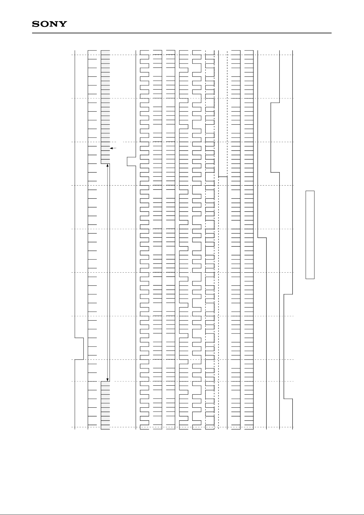
700 605040302010620610
123456789101112
CXD2443Q
Display start
25H
600
598
599
EVEN FIELD (standard HSYNC input)
Note) The FRP polarity is not specified for each line and field.
(BLK) in the timing chart is a pulse indicated as a reference and is not a pulse output from pins.
VD
VP1, 2, 3, 4: LLLH VM0J, 1J, 2J, 3J, 4J, 5J, 6J, 7J, 8J, 9J: LLLLLLLLL VM0J, 1J, 2J, 3J, 4J, 5J, 6J, 7J, 8J, 9J: LLLLHLLLL
MA: L SL3B: L VPOL: H SNSL: L NT-PL: L XHD: H
HSYNC
(BLK)
PAL (pulse eliminate display, standard HSYNC input) Vertical Direction Timing Chart
VST
HDR
HSTA
HSTB
ENB
VCK
FRP (1H inversed)
PCG1
PCG2
FRP (1F inversed)
FLDO
VWA
VWB
– 52 –
Page 53

700 60504030201011201110
CXD2443Q
Display start
1 2 3 4 5 6 7 8 9 10111213 1415 16 171819202122232425 26 2728
45H
1033 1035
ODD FIELD
1034
Note) The FRP polarity is not specified for each line and field.
(BLK) in the timing chart is a pulse indicated as a reference and is not a pulse output from pins.
VD
VP1, 2, 3, 4: LLLH VM0J, 1J, 2J, 3J, 4J, 5J, 6J, 7J, 8J, 9J: LLLLLLLLL VM0J, 1J, 2J, 3J, 4J, 5J, 6J, 7J, 8J, 9J: LLLLHLLLL
MA: H SL3B: L VPOL: H XHD: L
HSYNC
(BLK)
HD Vertical Direction Timing Chart
VST
HDR
HSTA
HSTB
ENB
VCK
FRP (1H inversed)
PCG1
PCG2
FRP (1F inversed)
FLDO
VWA
VWB
– 53 –
Page 54
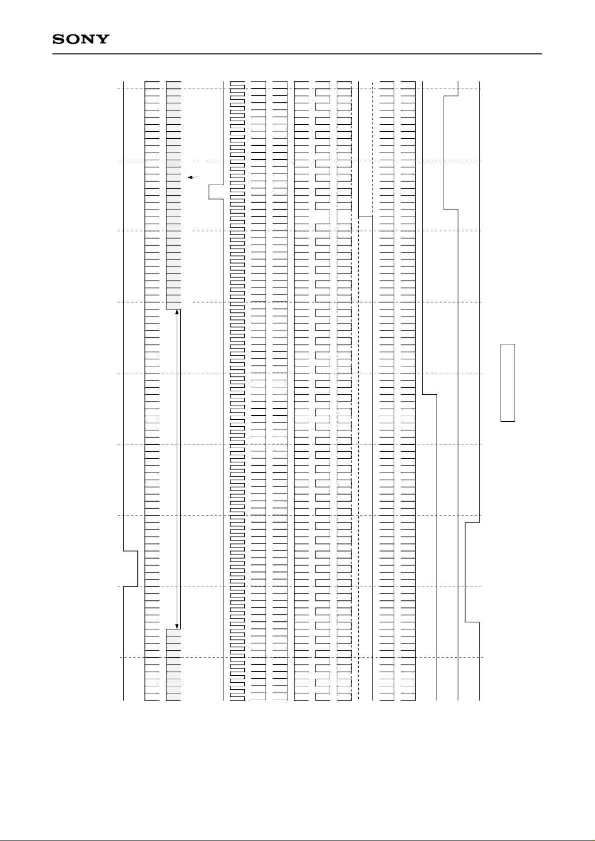
633563 623613603593583573
544
542
540
538
536
534
532
530
528
526
524
522
520
518
545
543
541
539
537
535
533
531
529
527
525
523
521
519
CXD2443Q
Display start
553
45H
515 517
EVEN FIELD
516
Note) The FRP polarity is not specified for each line and field.
VD
(BLK)
HSYNC
VP1, 2, 3, 4 : LLLH VM0J, 1J, 2J, 3J, 4J, 5J, 6J, 7J, 8J, 9J: LLLLLLLLL VM0J, 1J, 2J, 3J, 4J, 5J, 6J, 7J, 8J, 9J: LLLLHLLLL
MA: H SL3B: L VPOL: H XHD: L
HD Vertical Direction Timing Chart
VST
HDR
HSTA
HSTB
ENB
VCK
FRP (1H inversed)
PCG1
PCG2
FRP (1F inversed)
FLDO
VWA
VWB
– 54 –
(BLK) in the timing chart is a pulse indicated as a reference and is not a pulse output from pins.
Page 55
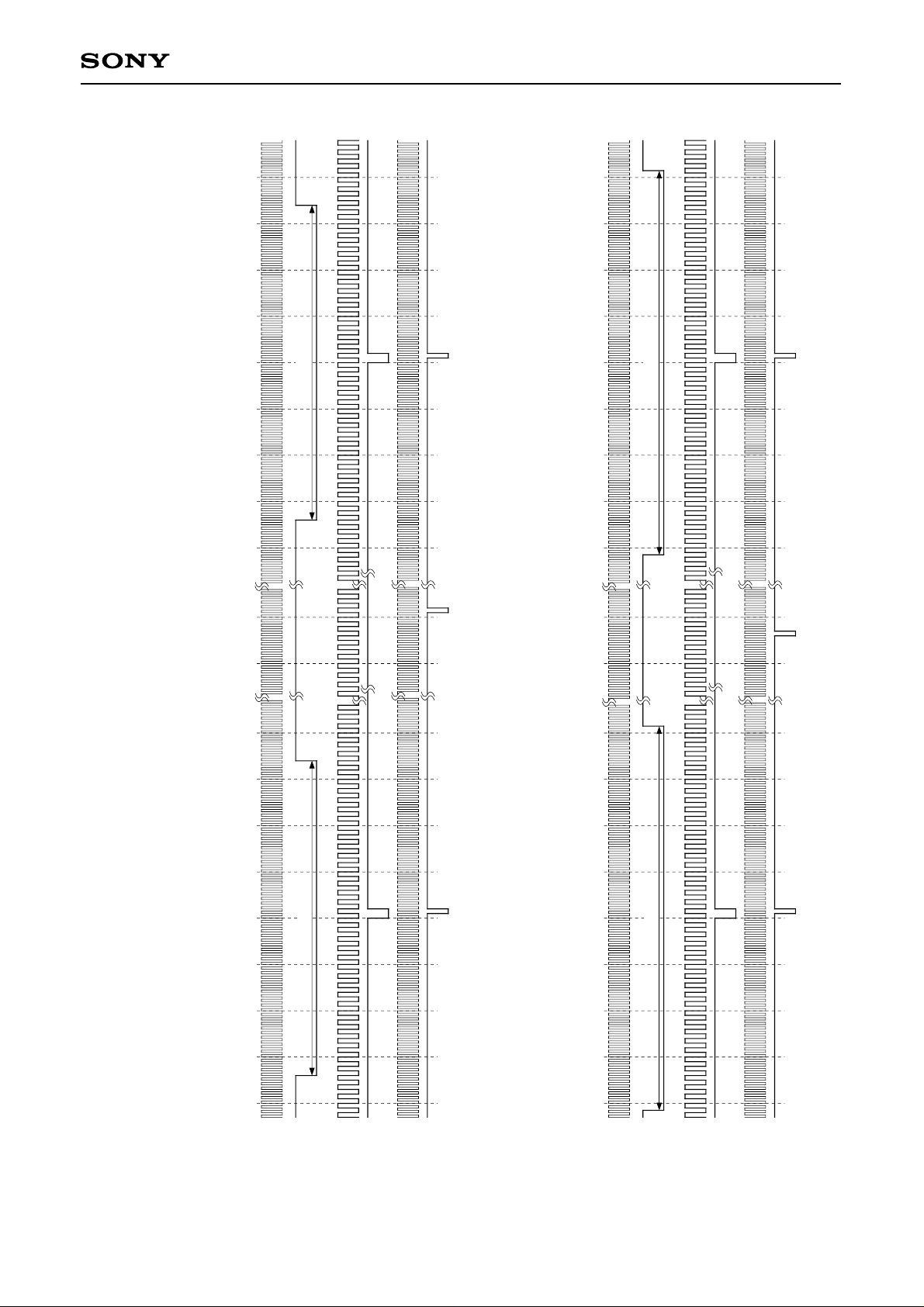
010203040
CXD2443Q
4.7µs (68fH)
4.7µs (83fH)
900 910 1780 1790 1800 1810
40 30 20 10 0 10 20 30 40
1130 1140 2230 2240 2250 2260
H, Master Clock 35.5MHz
4.7µs (68fH)
40 30 20 10 0 10 20 30 40 0 10 20 30 40
4.7µs (83fH)
NTSC Loop counter 910fH, Master Clock 28.6MHz
Line Double-Speed Timing Chart
SLBA = L
MCK
HSYNC
WCK
RSTW
RCK
RSTR
– 55 –
PAL Loop counter 1135f
MCK
HSYNC
WCK
RSTW
RCK
RSTR
Page 56

Application Circuit
RPD4 FPD4
0.01µ
1M
+13V
10k
3.3µ
10k
3.3µ
16V
16V
50k
33µ
25V
+5V
25V
25V
100p33µ
33µ
33µ
5.1k
0.1µ 33k
+13V
5.1k
0.1µ 33k
+13V
0.1µ
33k
50k
0.01µ
1k
0.01µ
RPD2 FPD2
1k
0.01µ
16V
FPD3RPD3
+5V
1M
680
0.01µ
10k
3.3µ
5.1k
16V
0.01µ
0.01µ
CXD2443Q
+5V
1M
1M
L : NTSC 1.8µH
1000p
PAL 1.2µH
33k
10k
50k
3.3k
1M
33k
10k
50k
3.3k
50k
0.01µ
16V
33k
1000p
D3
10k
3.3k
+5V
100p33µ
0.33µ
0.01µ
D4
0.01µ
1000p
D2
0.01µ
L
µPD485505
CKO4
PEO1
33k
3.3k
73
8
72
RSTW
PWM1
9
10k
WCK
RPD1
1000p
(NEC)
71
70
RCK
RSTR
CKI1
CKO1
10
11
0.68µ
D1
0.01µ
22p
+5V
1M
0.39µ
62p
+5V
47p
16V
50k
0.01µ
0.1µ 47µ
16V
SS
V
VWB
1M
+13V
75
78
3
74
7677
VDD
CKI4
FPD4
RPD4
DD
TC1
VSS
V
FPD1
6
5
4
7
0.1µ
33k
50k
33µ
0.01µ
25V
80
79
PEO4
81
PWM4
82
TC4
83
TC2
84
FPD2
85
PEO2
86
PWM2
87
RPD2
88
CKO2
89
CKI2
90
SS
V
91
CKO3
92
CKI3
93
RPD3
94
PEO3
95
PWM3
96
FPD3
TC3
97
98
CKSL
99
CKI5
HDR
100
XCLR
1
2
33k
47µ
1µ 0.1µ
16V
RPD1
+5V
1k
100p33µ
0.01µ
FPD1
1M
5.1k
10k
3.3µ
16V
69
TEST10
TEST2
12
50k
100p
68
SH7B
HSYNC
13
47p
67
14
33µ
16V
66
SH6B
VSYNC
15
+5V
65
SH5B
SS
V
16
0.01µ
0.1µ
64
SS
V
SCTR
17
63
SH4B
SCLK
18
62
SH3B
SDAT
19
SH2B
PRE
61
SH1B
TEST11
20
60
21
59
TEST9
FLDO
22
OFF
ON
PRE
0.1µ 47µ
55
57
58
56
54
SS
SH5A
TEST4
24
SH4A
TEST5
25
0.1µ
V
SH3A
TEST7
TEST6
26
27 282930
SH7A
TEST1
23
SH6A
TEST3
+5V
16V
53
52
51
VDD
SH1A
SH2A
50
XFRP
49
FRP
48
XCLP2
XCLP1
47
46
PCG2
45
XRGT
44
RGT
43
HSTA
HSTB
42
HCK1B
41
40
SS
V
HCK2B
39
38
HCK1A
37
HCK2A
ENB
36
35
VCK
VST
34
TEST8
33
32
DWN
PCG1
31
DD
SS
V
VWA
V
+5V
0.1µ 47µ
16V
Sync signal
Serial I/F
D1, D2, D3, D4 : 1T363A (Sony)
Application circuits shown are typical examples illustrating the operation of the devices. Sony cannot assume responsibility for
any problems arising out of the use of these circuits or for any infringement of third party patent and other right due to same.
– 56 –
Page 57
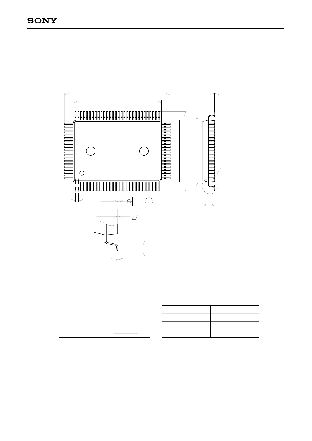
Package Outline Unit: mm
100PIN QFP (PLASTIC)
23.9 ± 0.4
+ 0.4
20.0 – 0.1
+ 0.4
17.9 ± 0.4
14.0 – 0.01
CXD2443Q
+ 0.1
0.15 – 0.05
15.8 ± 0.4
A
0.65
SONY CODE
EIAJ CODE
JEDEC CODE
0° to 15°
±0.12
DETAIL A
QFP-100P-L01
∗QFP100-P-1420-A
M
0.15
(16.3)
0.8 ± 0.2
2.75 – 0.15
PACKAGE STRUCTURE
PACKAGE MATERIAL
LEAD TREATMENT
LEAD MATERIAL
PACKAGE WEIGHT
EPOXY RESIN
SOLDER PLATING
COPPER / 42 ALLOY
1.4g
+ 0.35
– 57 –
 Loading...