

Page 1

Timing Generator for LCD Panels
For the availability of this product, please contact the sales office.
Description
The CXD2436Q is a timing signal generator for the
VGA LCD panel LCX012 driver. This chip has a
built-in serial interface circuit which allows the mode
to be switched with respect to various VGA signals
through direct control from an external
microcomputer, etc.
Features
• Generates the LCX012 drive pulse.
• Supports three-panel projectors.
• Built-in serial interface circuit
• Supports various VGA signals. (non-interlaced
mode)
• Built-in 2-line pair drive circuits
• Supports NTSC and PAL systems.
• Supports up/down and/or right/left inversion.
• Supports line inversion and field inversion.
• Generates timing signal of external sample-and-
hold circuit.
Applications
LCD projectors, etc.
CXD2436Q
100 pin QFP (Plastic)
Absolute Maximum Ratings (Ta=25 °C)
• Supply voltage VDD VSS–0.5 to +7.0 V
• Input voltage VI VSS–0.5 to VDD+0.5 V
• Output voltage VO VSS–0.5 to VDD+0.5 V
• Operating temperature
Topr –20 to +75 °C
• Storage temperature
Tstg –55 to +150 °C
Recommended Operating Conditions
• Supply voltage VDD +4.5 to +5.5 V
• Supply voltage VCC –20 to +75 °C
Structure
Silicon gate CMOS IC
Sony reserves the right to change products and specifications without prior notice. This information does not convey any license by
any implication or otherwise under any patents or other right. Application circuits shown, if any, are typical examples illustrating the
operation of the devices. Sony cannot assume responsibility for any problems arising out of the use of these circuits.
—1—
E95810-TE
Page 2

Block Diagram
CXD2436Q
EXT-CKI
CKI
CKO
HPOL
VPOL
CSYNC
HD2IN
VD2IN
HD1IN
VD1IN
TST1
TST2
TST3
TST4
TST5
TST6
TST7
TST8
TST9
TST10
VCK
VST1
VDO
SLDWN
SLMNB
DWN
PRG
XCLP1
XCLP2
HST
HCK1
HCK2
CLR
ENB
INT
PCG
SH1
SH2
SH3
SH4
SH5
SH6
SH7
30
34
33
16
17
14
20
21
23
24
25
26
27
37
50
92
93
72
11
19
71
75
76
77
84
85
86
87
88
89
91
94
95
96
97
98
99
100
283 53 78 4 15 29 40 42 45 46 47 48 49 51 52 54 65 79 90 22
SS
SS
SS
SS
SS
SS
SS
DD
DD
V
DD
V
V
SS
DD
V
V
SS
SS
V
V
SS
SS
V
V
V
V
V
V
V
V
V
MASTER CLOCK
6
7
PLL PHASE COMPARATOR
5
H-SYNC DETECTOR
H-SKEW DETECTOR
1
2
PLL COUNTER
V-SYNC SEPARATOR
V-RESET PULSE GENERATOR
SERIAL INTERFACE
V-RESET PULSE GENERATOR
V-POSITION COUNTER
V-TIMING PULSE
H-POSITION COUNTER
H-TIMING PULSE
GENERATOR
&
PULSE ELIMINATOR
FIELD & LINE CONTROLLER
AUX-VD COUNTER
SS
V
SS
SS
V
V
DIRECT CLEAR
GENERATOR
PWM
SS
NC
V
32
31
8
9
10
18
36
35
38
39
68
69
73
74
41
43
44
55
56
57
58
59
60
61
62
63
64
66
67
12
82
83
80
81
70
13
PEO
XCLR
PLNT
VGAV
SLSY
SLCKI
RPD
FPD
TC
HDN
XHDN
HDO
XHDO
SCK
SI
CS
PO0
PO1
PO2
PO3
PO4
PO5
PO6
PO7
PO8
PO9
PO10
PO11
SLRGT
RGT
XRGT
FRP
XFRP
FLD
SLFR
—2—
Page 3
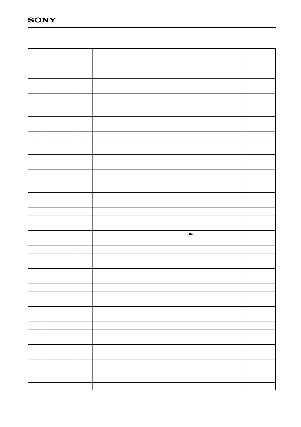
Pin Description
CXD2436Q
Pin
No.
1
2
3
4
5
6
7
8
9
10
11
12
13
14
15
16
17
18
19
20
21
22
23
24
25
26
27
28
29
30
31
32
33
34
35
36
37
38
Symbol
HD1IN
VD1IN
VDD
VSS
CSYNC
HPOL
VPOL
XCLR
PLNT
VGAV
SLDWN
SLRGT
SLFR
TST1
VSS
HD2IN
VD2IN
SLSY
SLMNB
TST2
TST3
N.C.
TST4
TST5
TST6
TST7
TST8
VDD
VSS
EXT-CKI
PEO
PWM
CKO
CKI
RPD
SLCKI
TST9
FPD
I/O
I
I
—
—
I
I
I
I
I
I
I
I
I
I
—
I
I
I
I
I
I
—
—
—
—
—
—
—
—
I
I/O
I
I/O
I
O
I
I
O
Description
Hsync input (VGA)
Vsync input (VGA)
Power supply
GND
Composite sync input (NTSC/PAL)
HD, CSYNC polarity identification input
(High: positive polarity, Low: negative polarity)
VD, CSYNC polarity identification input
(High: positive polarity, Low: negative polarity)
External clear (all clear when Low)
PAL/NTSC switching (High: NTSC, Low: PAL)
VGA (NTSC/PAL) switching (High: VGA, Low: NTSC/PAL)
Up/down inversion discrimination signal input
(High: Down, Low: Up)
Right/left inversion discrimination signal input
(High: Normal, Low: Reverse)
1H/1F inversion switching (High: 1H, Low: 1F)
Test pin (Not connected or High.)
GND
HD2 input (for NTSC/PAL separate-sync)
VD2 input (for NTSC/PAL separate-sync)
SYNC input switching (High: CSYNC, Low: HD2IN and VD2IN)
Switches mode (High: Nothing, Low: 400 480 line conversion)
Test pin (Not connected or High.)
Test pin (Connect to GND.)
N.C.
Test pin (Not connected or High.)
Test pin (Not connected or High.)
Test pin (Not connected or High.)
Test pin (Not connected.)
Test pin (Connect to GND.)
Power supply
GND
External clock input
Loop filter integrator output
Loop filter integrator input
Oscillation cell output (NTSC/PAL)
Oscillation cell input (NTSC/PAL)
Phase comparator output (NTSC/PAL)
Clock input selection (High: CKI, Low: EXT-CKI)
(NTSC/PAL mode only)
Test pin (Not connected or High.)
Phase comparator output (NTSC/PAL)
Input pin for
open status
—
—
—
—
—
H
H
H
H
H
H
H
H
H
—
—
—
H
H
H
H
—
—
—
—
—
—
—
—
—
—
—
—
—
—
H
H
—
—3—
Page 4
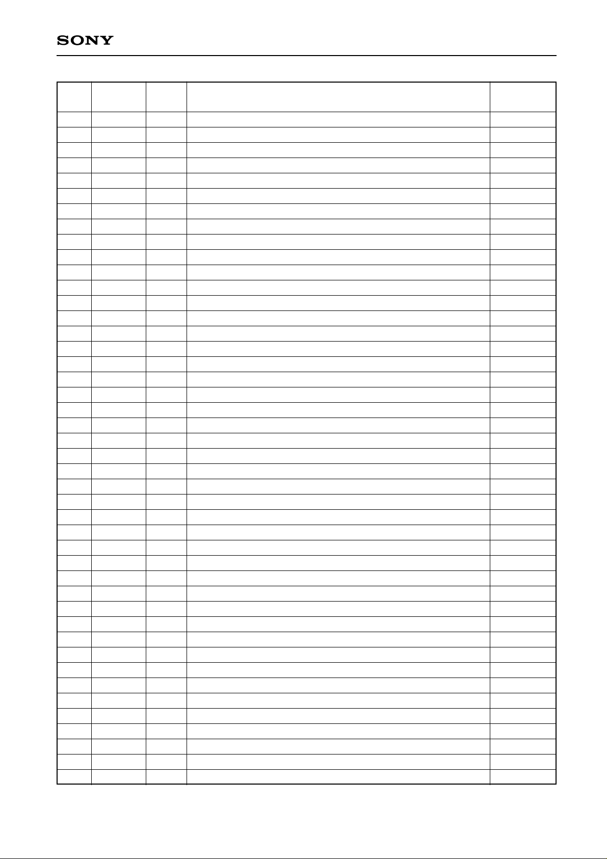
CXD2436Q
Pin
No.
39
40
41
42
43
44
45
46
47
48
49
50
51
52
53
54
55
56
57
58
59
60
61
62
63
64
65
66
67
68
69
70
71
72
73
74
75
76
77
78
79
80
81
82
Symbol
TC
VSS
SCK
VSS
SI
CS
VSS
VSS
VSS
VSS
VSS
TST10
VSS
VSS
VDD
VSS
PO0
PO1
PO2
PO3
PO4
PO5
PO6
PO7
PO8
PO9
VSS
PO10
PO11
HDN
XHDN
FLD
DWM
VDO
HDO
XHDO
PRG
XCLP1
XCLP2
VDD
VSS
FRP
XFRP
RGT
I/O
I/O
—
I
—
I
I
—
—
—
—
—
I
—
—
—
—
O
O
O
O
O
O
O
O
O
O
—
O
O
O
O
O
O
O
O
O
O
O
O
—
—
O
O
O
Description
FPD pin pulse width adjustment
GND
Serial interface clock input
GND
Serial interface data input
Serial interface chip select
GND
GND
GND
GND
GND
Test pin (Not connected or High.)
GND
GND
Power supply
GND
Serial I/O data output
Serial I/O data output
Serial I/O data output
Serial I/O data output
Serial I/O data output
Serial I/O data output
Serial I/O data output
Serial I/O data output
Serial I/O data output
Serial I/O data output
GND
Serial I/O data output
Serial I/O data output
Phase comparator output (positive polarity)
Phase comparator output (negative polarity)
Field discrimination signal output
Up/down inversion discrimination signal output
VD pulse output (positive polarity)
HD pulse output (positive polarity)
HD pulse output (negative polarity)
Precharge signal pulse (positive polarity)
Pedestal clamp pulse 1
Pedestal clamp pulse 2
Power supply
GND
AC drive inversion timing output
AC drive inversion timing output
Right/left inversion discrimination signal output
Input pin for
open status
—
—
H
—
L
H
—
—
—
—
—
H
—
—
—
—
—
—
—
—
—
—
—
—
—
—
—
—
—
—
—
—
—
—
—
—
—
—
—
—
—
—
—
—
—4—
Page 5
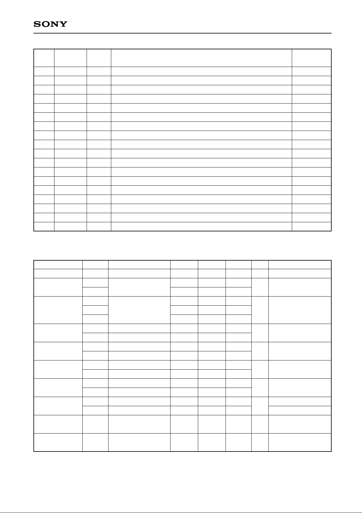
CXD2436Q
Pin
No.
83
84
85
86
87
88
89
90
91
92
93
94
95
96
97
98
99
100
Symbol
XRGT
HST
HCK1
HCK2
CLR
ENB
INT
VSS
PCG
VCK
VST1
SH1
SH2
SH3
SH4
SH5
SH6
SH7
I/O
O
O
O
O
O
O
O
O
O
O
O
O
O
O
O
O
O
O
Description
Right/left inversion discrimination signal output
H start pulse output (positive polarity)
H clock pulse 1 output
H clock pulse 2 output
CLR pin output
ENB pin output
INT pin output
GND
PCG pin output (positive polarity)
V clock pulse output
V start pulse output
Sample-and-hold pulse 1 (positive polarity)
Sample-and-hold pulse 2 (positive polarity)
Sample-and-hold pulse 3 (positive polarity)
Sample-and-hold pulse 4 (positive polarity)
Sample-and-hold pulse 5 (positive polarity)
Sample-and-hold pulse 6 (positive polarity)
Sample-and-hold pulse 7 (positive polarity)
Input pin for
open status
—
—
—
—
—
—
—
—
—
—
—
—
—
—
—
—
—
—
Electrical Characteristics
1. DC characteristics (Temperature = 25 °C, VSS = 0 V)
Item Symbol Conditions Min. Typ. Max. Unit Applicable pins
Supply voltage
Input voltage 1
Input voltage 2
Output voltage 1
Output voltage 2
Output voltage 3
Output voltage 4
Input leak
current
Output leak
current
Current
consumption
VDD
VIH1
VIL1
VIH2
VIL2
VT+ –VT+
VOH
VOL
VOH
VOL
VOH
VOL
VOH
VOL
IIL
IIH
ILZ
IDD
CMOS input cell
CMOS Schmitt
0.7 VDD
0.8 VDD
trigger input cell
IOH=–2 mA
VDD–0.8
IOL=4 mA
IOH=–4 mA
VDD–0.8
IOL=8 mA
IOH=–6 mA
VDD–0.8
IOL=12 mA
IOH=–3 mA
VDD/2
IOL=3 mA
Pull-up resistor connected
Pull-down resistor connected
High impedance
status
fclk=31 MHz
VDD=5.0 V
4.5
–40
40
–40
5.0
0.6
–100
100
55
5.5
0.3 VDD
0.2 VDD
0.4
0.4
0.4
VDD/2
–240
240
40
V
Input pins other than
V
those noted below
HDnIN, VDnIN, CSYNC,
CKI, PWM, TC, PEO,
V
CKO, SI, SCK, CS
Output pins other than
V
those noted below
VCK
V
HCKn, SHn, HST
V
CKO, PEO
V
∗1
µA
SI
RPD, FPD
µA
At no load
mA
∗1
Input pins with pull-up resistors
HPOL, VPOL, XCLR, PLNT, VGAV, SLDWN, SLRGT, SLFR, TST1, SLSY, TST2, TST3, SLCKI, TST9, SCK, CS
—5—
Page 6

CXD2436Q
2. AC characteristics (VDD=5.0 V±0.5 V, VSS=0 V)
Item Applicable pins Symbol Conditions Min. Typ. Max. Unit
Clock input cycle
Cross-point time difference
Output rise delay
Output fall delay
Output rise delay
Output fall delay
HCK1, SH1 delay
time difference
HCK2, SH1 delay
time difference
HCK1 duty
HCK2 duty
EXT-CKI, CKI
HCK1, 2
HCKn, SHn
HCKn, SHn
Other than
HCKn and SHn
Other than
HCKn and SHn
HCK1, SH1
HCK2, SH1
HCK1
HCK2
∆t
tpr
tpf
tpr
tpf
dt1
dt2
tH/tH+tL
tH/tH+tL
CL=30 pF
CL=30 pF
CL=30 pF
CL=30 pF
CL=30 pF
CL=30 pF
CL=30 pF
CL=30 pF
CL=30 pF
25
–10
48
48
50
50
10
20
20
30
30
10
10
52
52
ns
ns
ns
ns
ns
ns
ns
ns
%
%
EXT-CKI/CKI
Output
Output
HCK1
50%
tpr
tpf
90%
10%
50%
VDD
0V
V
0V
VDD
0V
VDD
0V
DD
HCK2
V
DD
50%
∆t
50%
0V
∆t
—6—
Page 7

EXT-CKI
/CKI
CXD2436Q
HCK1
HCK2
SH1
50% 50%
t1
tH
50%
dt1
3. Serial interface block AC characteristics
SCK
50%
tw1
t2
tL
50%
dt2
(SLRGT=H, SHP0/SHP1/SHP2/SHP3=L)
tw1
50%
50%
50%
50%
SI (DATA)
CS
50%
50%
ts0
ts1
th1
50%
50%
th0
(VDD=5.0 V±0.5 V, VSS=0 V, Topr=–20 to +75 °C
Symbol Item Min. Max.
ts1
th1
tw1
ts0
th0
th1
SI setup time with respect to rise of SCK
SI hold time with respect to rise of SCK
SCK pulse width
CS setup time with respect to rise of SCK
CS hold time with respect to rise of SCK
SCK high-level hold time with respect to rise of CS
200 ns
200 ns
200 ns
200 ns
200 ns
200 ns
2tw1
2tw1
th1
—7—
Page 8
CXD2436Q
A
A
A
A
A
A
A
A
A
A
A
A
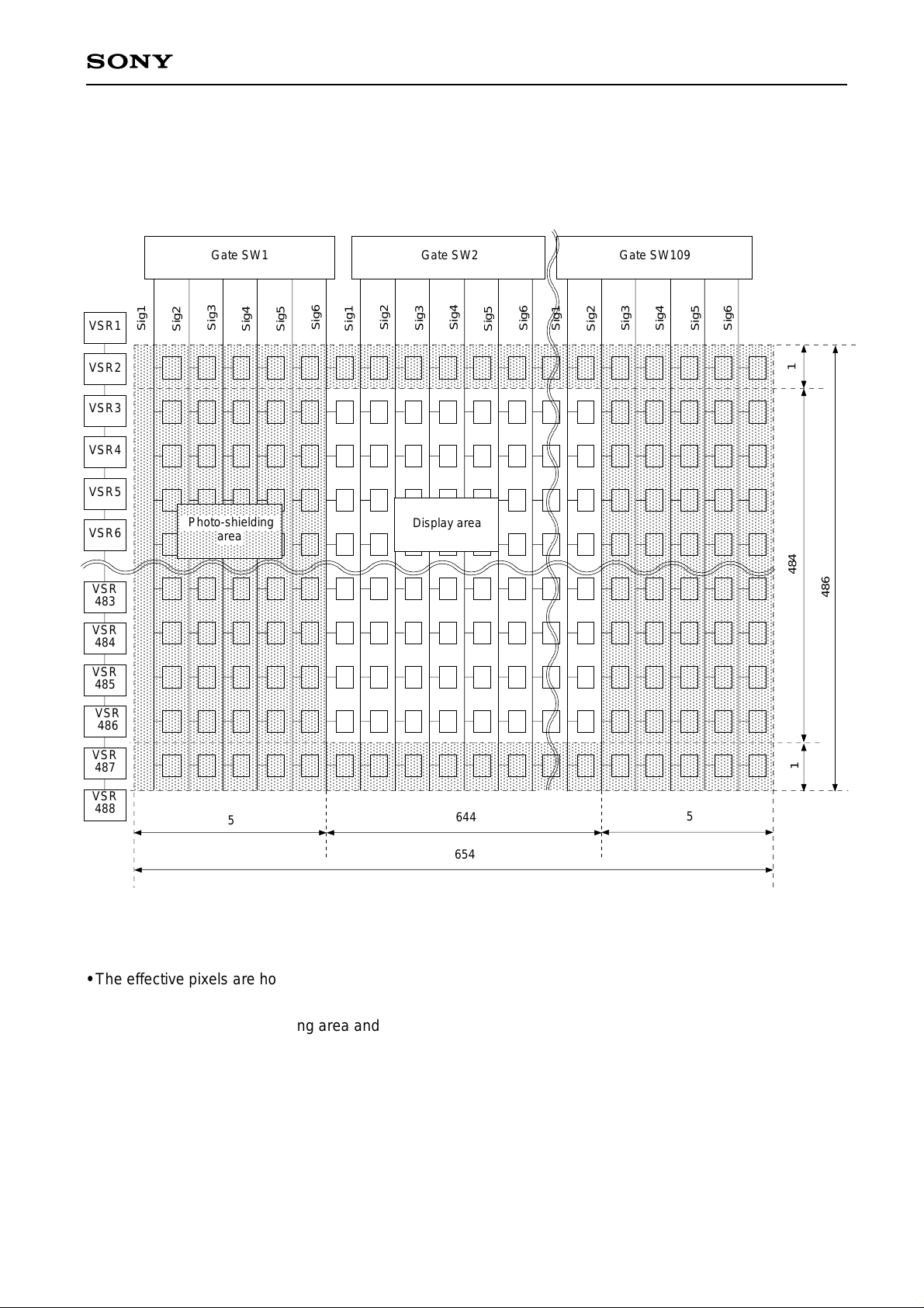
LCD Panel Structure
The structure of LCD panels (LCX012AL) driven by this IC is shown below.
The dot arrangement is a square arrangement, and the shaded region within the diagram is not displayed.
Gate SW1 Gate SW2 Gate SW109
VSR1
VSR2
VSR3
VSR4
VSR5
VSR6
VSR
483
VSR
484
VSR
485
VSR
486
VSR
487
VSR
488
Sig1
Sig2
Sig3
Sig4
Sig5
Sig6
Sig1
Sig2
Sig3
Sig4
Sig5
Sig6
Sig1
Sig2
Sig3
Sig4
Sig5
AAAAAAAAAAAAAAAA
AAAAAAAAAAAAAAAA
AAAAAAAAAAAAAAAA
AAAAAAAAAAAAAAAA
Photo-shielding
area
AAAAAAAAAAAAAAAA
AA
Display area
AAAAAAAAAAAAAAAA
AAAAAAAAAAAAAAAA
AAAAAAAAAAAAAAAA
AAAAAAAAAAAAAAAA
AAAAAAAAAAAAAAAA
AAAAAAAAAAAAAAAA
5
644
5
Sig6
1
484
486
1
654
• The effective pixels are horizontal: 644 pixels and vertical: 484 pixels.
• The horizontal pixel start position is from Sig6 of the first-stage scanner. (Sig1 to Sig5 of the first-stage
scanner are the photo-shielding area and are not displayed.)
• The vertical pixel start position is from the third-stage scanner.
• These relationships are the same even during up/down and/or right/left inversion. (The entire area within the
panel is inverted.)
—8—
Page 9
Description of Operation
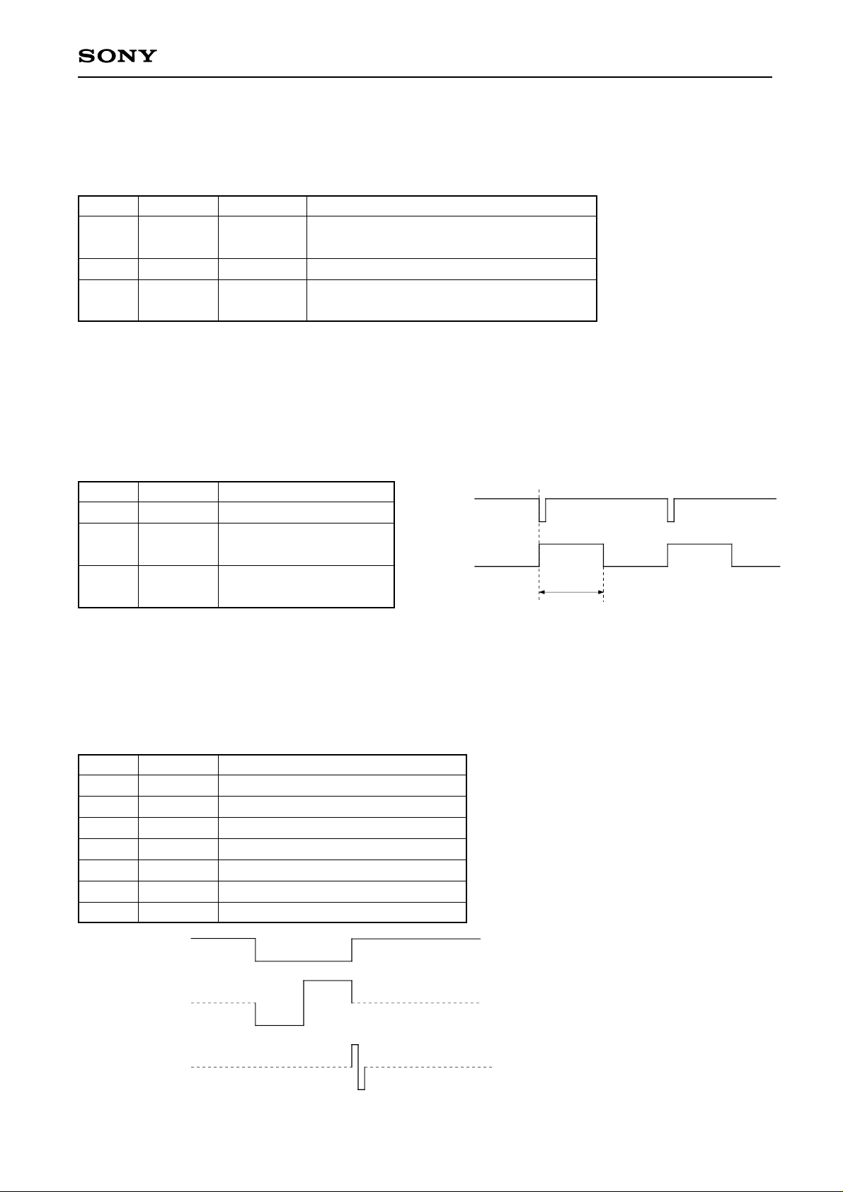
• Sync input pins
The CXD2436Q has three types of sync input pins.
Pin No. Symbol SLSY setting Application
HD1IN
16
17
1
VD1IN
2
CSYNC
5
HD2IN
VD2IN
—
H
SYNC input pins for VGA
CSYNC input pin for NTSC/PAL
L
Separate SYNC input pins for NTSC/PAL
• Clock input pins
The CXD2436Q has two clock input pin systems to support two types of PLL circuits.
1) When using EXT-CKI (using an external PLL IC)
The 1/N frequency divider output is output from the HDN and XHDN pins for the external PLL IC.
The used pins are shown in the following table. (SLCKI = Low)
CXD2436Q
Pin No. Symbol Application
30
68
69
EXT-CKI
HDN
XHDN
Clock input
Phase comparison output
(positive polarity)
Phase comparison output
(negative polarity)
HSYNC
HDN OUTPUT
400 clk
2) When using CKI
This system uses the built-in phase comparator and an externally attached VCO circuit (see the Application
Circuit).
This system is used during AV mode (NTSC/PAL).
The used pins are shown in the following table. (Effective when SLCKI is set to High.)
Pin No. Symbol Application
31
32
33
34
35
38
39
PEO
PWM
CKO
CKI
RPD
FPD
TC
Loop filter integrator output
Loop filter integrator input
Clock output (oscillation cell output)
Clock input (oscillation cell input)
Phase comparator output
Phase comparator output
FPD pin pulse width adjustment
HSYNC
RPD
FPD
An outline of the output waveforms during
PLL lock is shown in the figure to the left.
—9—
Page 10

CXD2436Q
• Connections supporting up/down and/or right/left inversion
The CXD2436Q is designed for use with three-panel projectors, and has a system configuration which
permits both normal and reverse scan. The RGT and XRGT output to the panel are switched according to
the SLRGT input, and the DWN output is switched according to the SLDWN input in the same manner.
SLRGT
SLDWN
12
11
Example of supporting a three-panel system
82
83
71
RGT
XRGT
DWN
LCX012
RGT
DWN
LCX012
RGT
DWN
LCX012
RGT
DWN
Normal scanning
panel
Normal scanning
panel
Reverse scanning
panel
• AC driving of LCD panels for no signal
The following measures have been adopted to allow AC driving of LCD panels even when there is no
signal.
• Horizontal direction pulse: The PLL is set to free running status. Therefore, the frequency of the
horizontal direction pulse is dependent on the PLL free running frequency.
• Vertical direction pulse: The number of lines is counted by an internal counter and VST and FRP
are output at a specified cycle.
• VST cycle for no signal • Free running detection timing
NTSC 269H
PAL 321H
VGA 526H
NTSC 291H
PAL 339H
VGA 873H
Free running operates at the following cycles.
(No signal is judged if there is no VSYNC input for longer than the following periods.)
• Description of the MODE selector switch
• VGA/AV (NTSC/PAL) switching is performed with two pins.
VGAV PLNT MODE
H H VGA
H L VGA
L H NTSC
L L PAL
• The HD1IN, HD2IN, VD1IN, VD2IN and CSYNC input polarities are supported by two pins.
HPOL VPOL
HD1IN VD1IN
HD2IN VD2IN
CSYNC
H H Positive polarity Positive polarity Positive polarity
H L Positive polarity Negative polarity —
L H Negative polarity Positive polarity —
L L Negative polarity Negative polarity Negative polarity
—10—
Page 11
CXD2436Q
• XCLR (External clear)
Reset should be performed during startup in order to initialize the serial interface. Performing external
clear sets all serial interface modes to Low.
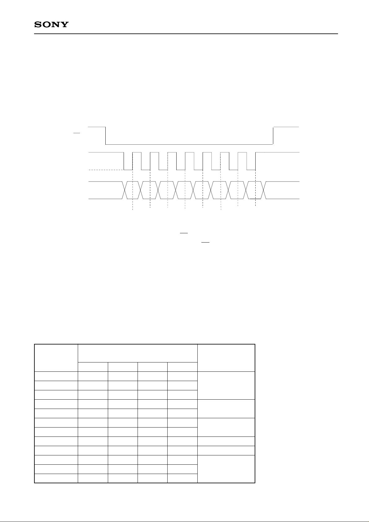
• Serial interface specifications
The CXD2436Q can set and switch the driving mode with the serial interface.
Set the corresponding timing data for each VGA signal according to the format in the diagram below. Be
sure to make the initial mode settings. (See the AC characteristics for detailed timing specifications.)
CS
SCK
SI
D0 D1 D2 D3 D4 D5 D6 D7
Fig. 1. Timing chart for the serial interface input block
Note) D0 to D7 internal transfer is completed by the CS signal switching from a Low to High pulse. Therefore,
the data should be transferred in 1-byte units with the CS signal reset each time.
• Description of mode switching settings using the serial interface
The CXD2436Q can set the following six modes.
(1) Frequency division ratio setting for the 1/N frequency divider of the master clock PLL circuit block.
(2) H screen center adjustment. The center changes by one dot with LSB.
(3) V screen center adjustment. The center changes by one line with LSB.
(4) Sample-and-hold circuit phase adjustment. The phase changes by a half-dot with LSB.
(See the Description of Sample-and-Hold Timing for details.)
(5) Clamp pulse timing adjustment (4-way)
(6) Data output (Serial data is held and output.)
Upper 4-bit
address value
D7 to D4
0H
1H
2H
3H
4H
5H
6H
7H
8H
9H
AH
BH
D3
PHP3
PHP7
—
HP3
—
VP3
—
SHP3
—
PO3
PO7
PO11
Lower 4-bit data
D2
PHP2
PHP6
PHP10
HP2
HP6
VP2
VP6
SHP2
—
PO2
PO6
PO10
D1
PHP1
PHP5
PHP9
HP1
HP5
VP1
VP5
SHP1
CLPP1
PO1
PO5
PO9
D0
PHP0
PHP4
PHP8
HP0
HP4
VP0
VP4
SHP0
CLPP0
PO0
PO4
PO8
Functions
PLL 1/N frequency
divisions
H screen center
adjustment
V screen center
adjustment
S/H timing
Clamp timing
Data output
∗ PHP0, HP0, VP0, SHP0, CLPP0
—11—
Page 12
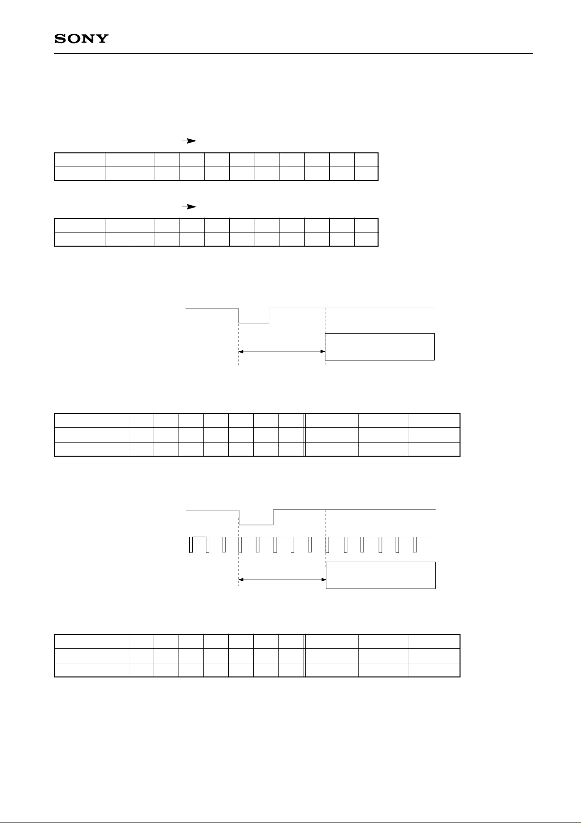
• PLL 1/N frequency division ratio setting
For the frequency division ratio setting during VGA mode, set the value of the number of dots for the
horizontal period –1 in PHP0-10.
(Example) When the horizontal period is set to 800 dots
PHP setting value = 800-1 799 (01100011111 LSB)
PHP 10 9 8 7 6 5 4 3 2 1 0
01100011111
Set the value of the number of dots fixed to 816 during NTSC/PAL.
PHP setting value = 816-1 815 (01100101111 LSB)
PHP 10 9 8 7 6 5 4 3 2 1 0
01100101111
• Horizontal position setting
The horizontal display start position setting can be changed one dot at a time by the HP0 to 6 setting.
HSYNC
CXD2436Q
Thp
644dots
Image display period
The maximum and minimum Thp values which can be set are shown in the following table.
HP 6543210
Minimum value 1111111
Maximum value 0000000
VGA NTSC PAL
110 dots 5.8 µs 5.8 µs
237 dots 15.7 µs 15.8 µs
• Vertical position setting
The vertical display start position setting can be changed one dot at a time by the VP0 to 6 setting.
VSYNC
HSYNC
Tvp
484 line
Image display period
The maximum and minimum Tvp values which can be set are shown in the following table.
VP 6543210
Minimum value 1111111
Maximum value 0000000
(This table shows the ODD field values for NTSC and PAL.)
—12—
VGA NTSC PAL
5 H 14 H 14 H
133 H 141 H 141 H
Page 13
CXD2436Q
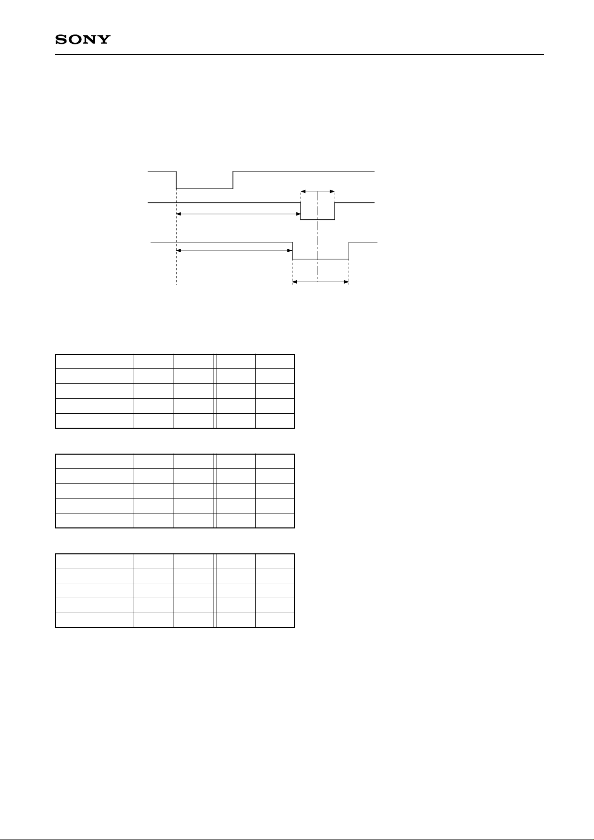
• CLP pulse position setting
The XCLP pulse position can be changed to four different positions. Each of these positions is shown
below.
The XCLP pulse is linked with the horizontal position setting, and is indicated with the HP (1000000 LSB)
setting.
HSYNC
Wclp1
XCLP1
tclp1
XCLP2
tclp2
• VGA mode
CLPP1 CLPP0 tclp1 Wclp1 tclp2 Wclp2
0 0 74 dot 40 dot 61 dot 67 dot
0 1 81 dot 40 dot 68 dot 67 dot
1 0 88 dot 40 dot 75 dot 67 dot
1 1 95 dot 40 dot 82 dot 67 dot
• NTSC mode
CLPP1 CLPP0 tclp1 Wclp1 tclp2 Wclp2
0 0 4.83 µs 1.17 µs 4.36 µs 2.18 µs
0 1 5.30 µs 1.17 µs 4.83 µs 2.18 µs
1 0 5.76 µs 1.17 µs 5.30 µs 2.18 µs
1 1 6.23 µs 1.17 µs 5.76 µs 2.18 µs
The centers of the XCLP1
and XCLP2 pulses match.
Wclp2
• PAL mode
CLPP1 CLPP0 tclp1 Wclp1 tclp2 Wclp2
0 0 4.87 µs 1.18 µs 4.39 µs 2.20 µs
0 1 5.33 µs 1.18 µs 4.86 µs 2.20 µs
1 0 5.80 µs 1.18 µs 5.33 µs 2.20 µs
1 1 6.27 µs 1.18 µs 5.80 µs 2.20 µs
—13—
Page 14
CXD2436Q
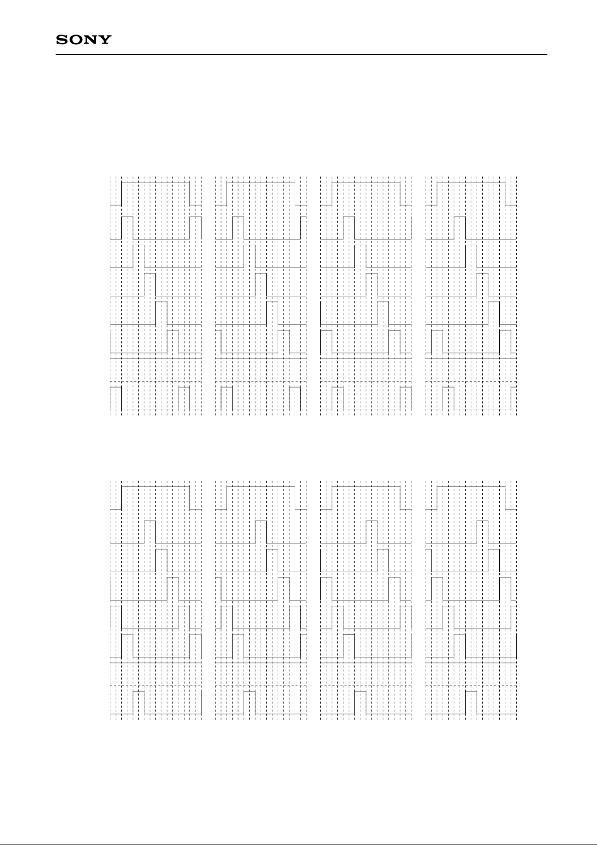
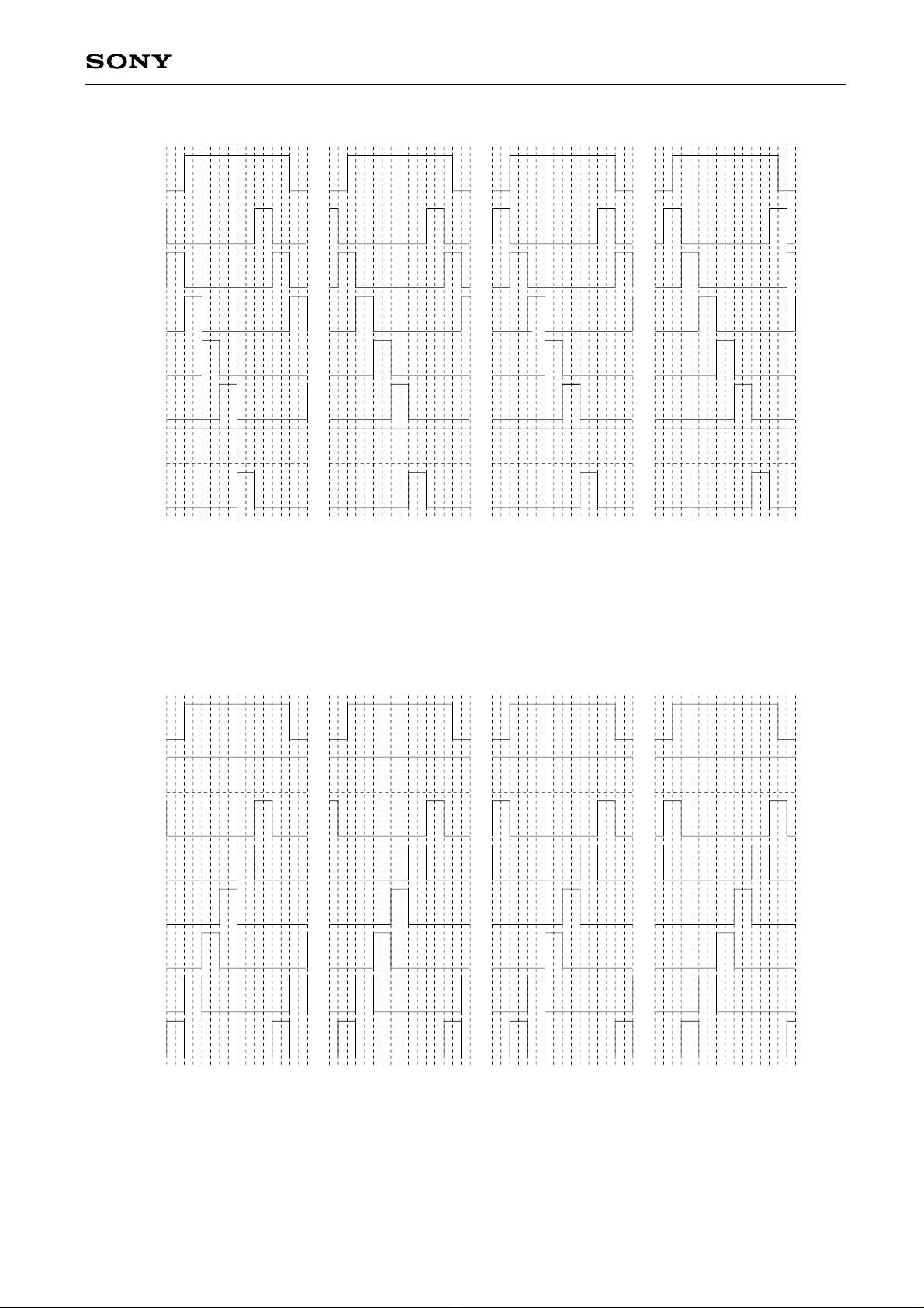
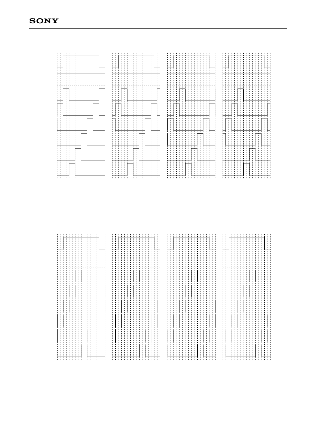
• Switching the SH pulse timing
The phase relationship between the sample-and-hold pulses and HCK can be switched in 12 different ways
with SHP0, SHP1, SHP2 and SHP3.
(This timing generator has a 0.5 DOT OFFSET function in order to ensure the phase margin.)
In addition, the timing differs according to the scanning direction (right/left scan).
Right scanning pulse (RGT = H)
HCK
SH1
SH2
SH3
SH4
SH5
SH6
SH7
HCK
SH1
SH2
SH3
SH4
SHP0=L
SHP1=L
SHP2=L
SHP3=L
SHP0=H
SHP1=L
SHP2=L
SHP3=L
SHP0=L
SHP1=H
SHP2=L
SHP3=L
SHP0=H
SHP1=H
SHP2=L
SHP3=L
SH5
SH6
SH7
SHP0=L
SHP1=L
SHP2=H
SHP3=L
SHP0=H
SHP1=L
SHP2=H
SHP3=L
—14—
SHP0=L
SHP1=H
SHP2=H
SHP3=L
SHP0=H
SHP1=H
SHP2=H
SHP3=L
Page 15
HCK
SH1
SH2
SH3
SH4
SH5
SH6
SH7
CXD2436Q
HCK
SH1
SH2
SH3
SH4
SH5
SHP0=L
SHP1=L
SHP2=L
SHP3=H
SHP0=H
SHP1=L
SHP2=L
SHP3=H
Left scanning pulse (RGT = L)
SHP0H=L
SHP1=H
SHP2=L
SHP3=H
SHP0=H
SHP1=H
SHP2=L
SHP3=H
SH6
SH7
SHP0=L
SHP1=L
SHP2=L
SHP3=L
SHP0=H
SHP1=L
SHP2=L
SHP3=L
—15—
SHP0=L
SHP1=H
SHP2=L
SHP3=L
SHP0=H
SHP1=H
SHP2=L
SHP3=L
Page 16
HCK
SH1
SH2
SH3
SH4
SH5
SH6
SH7
CXD2436Q
HCK
SH1
SH2
SH3
SH4
SH5
SH6
SHP0=L
SHP1=L
SHP2=H
SHP3=L
SHP0=H
SHP1=L
SHP2=H
SHP3=L
SHP0=L
SHP1=H
SHP2=H
SHP3=L
SHP0=H
SHP1=H
SHP2=H
SHP3=L
SH7
SHP0=L
SHP1=L
SHP2=L
SHP3=H
SHP0=H
SHP1=L
SHP2=L
SHP3=H
—16—
SHP0=L
SHP1=H
SHP2=L
SHP3=H
SHP0=H
SHP1=H
SHP2=L
SHP3=H
Page 17
34fh
CXD2436Q
40fh
100fh
55fh
67fh
42fh
76fh
76fh
15fh
40fh
36fh
30fh
24fh
1fh
770 780 790 0 10 20 30 40 50 60 70 80 90 100 110 120 130 140 150 160 170 180 189
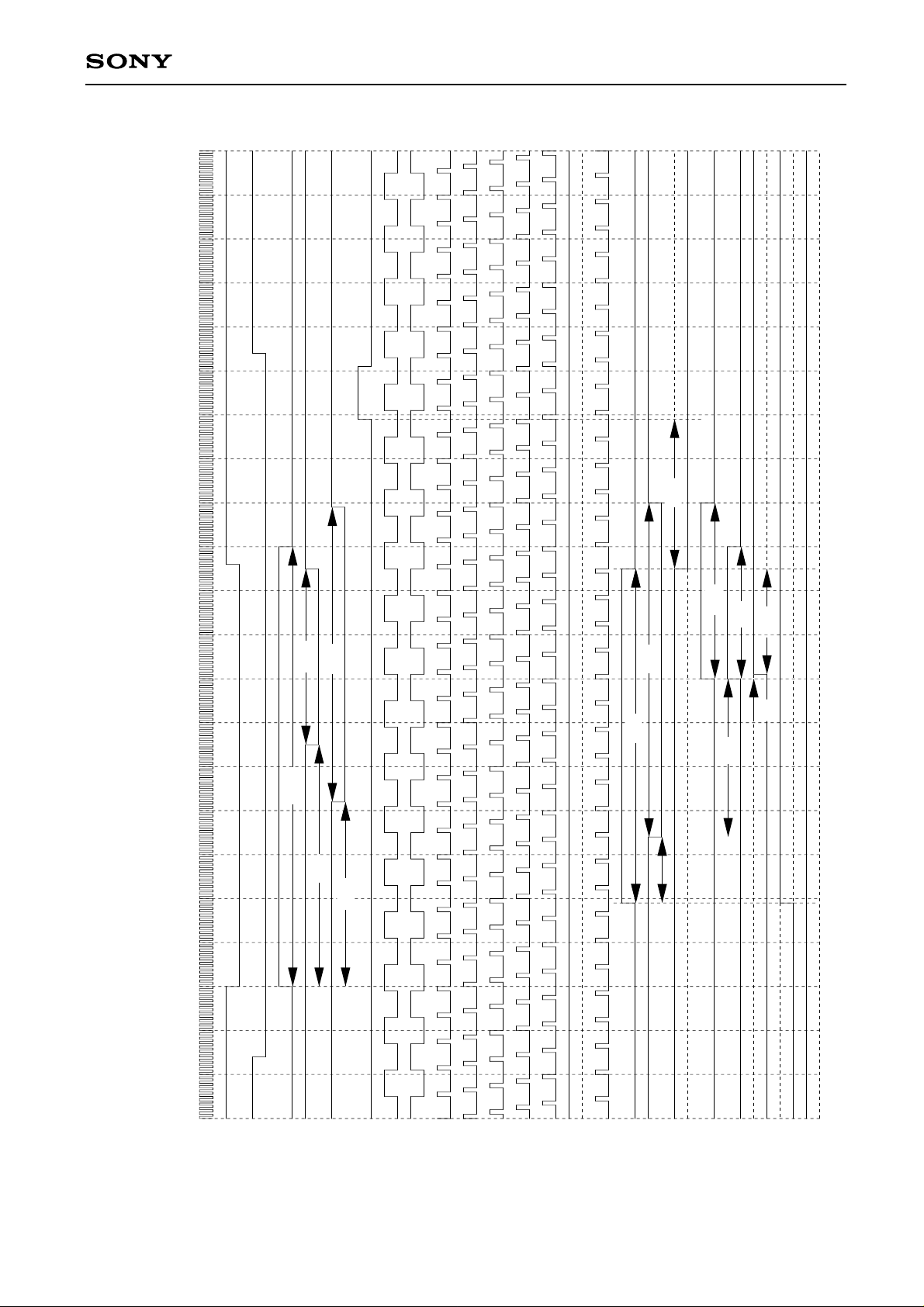
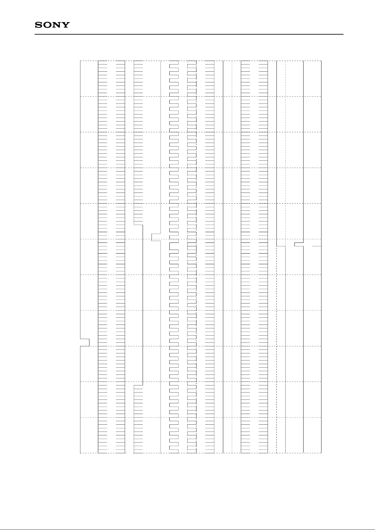
SLRGT: H (Normal scan)
HP: 1100001 LSB CLPP: 10 LSB SHP: 0000 LSB
SH2
MCK
Horizontal Direction Timing Chart (IBM-VGA 640 x 480)
CSYNC
(BLK)
/HD1IN
HDO
XCLP1
HST
XCLP2
HCK1
HCK2
SH1
—17—
SH3
SH4
SH5
SH6
SH7
CLR
ENB
VCK
PRG
PCG
FRP
VST1
INT
Page 18

34fh
CXD2436Q
40fh
100fh
55fh
67fh
42fh
76fh
76fh
15fh
40fh
36fh
30fh
24fh
1fh
770 780 790 0 10 20 30 40 50 60 70 80 90 100 110 120 130 140 150 160 170 180 189
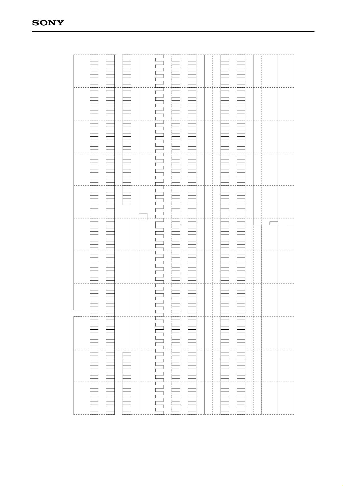
SLRGT: L (Reverse scan)
HP: 1100001 LSB CLPP: 10 LSB SHP: 0000 LSB
MCK
Horizontal Direction Timing Chart (IBM-VGA 640 x 480)
CSYNC
(BLK)
/HD1IN
HDO
XCLP1
HST
XCLP2
HCK1
HCK2
SH1
SH2
—18—
SH3
SH4
SH5
SH6
SH7
CLR
ENB
VCK
PRG
PCG
FRP
VST1
INT
Page 19
40 46
30
20
10
CXD2436Q
1
480
470
460
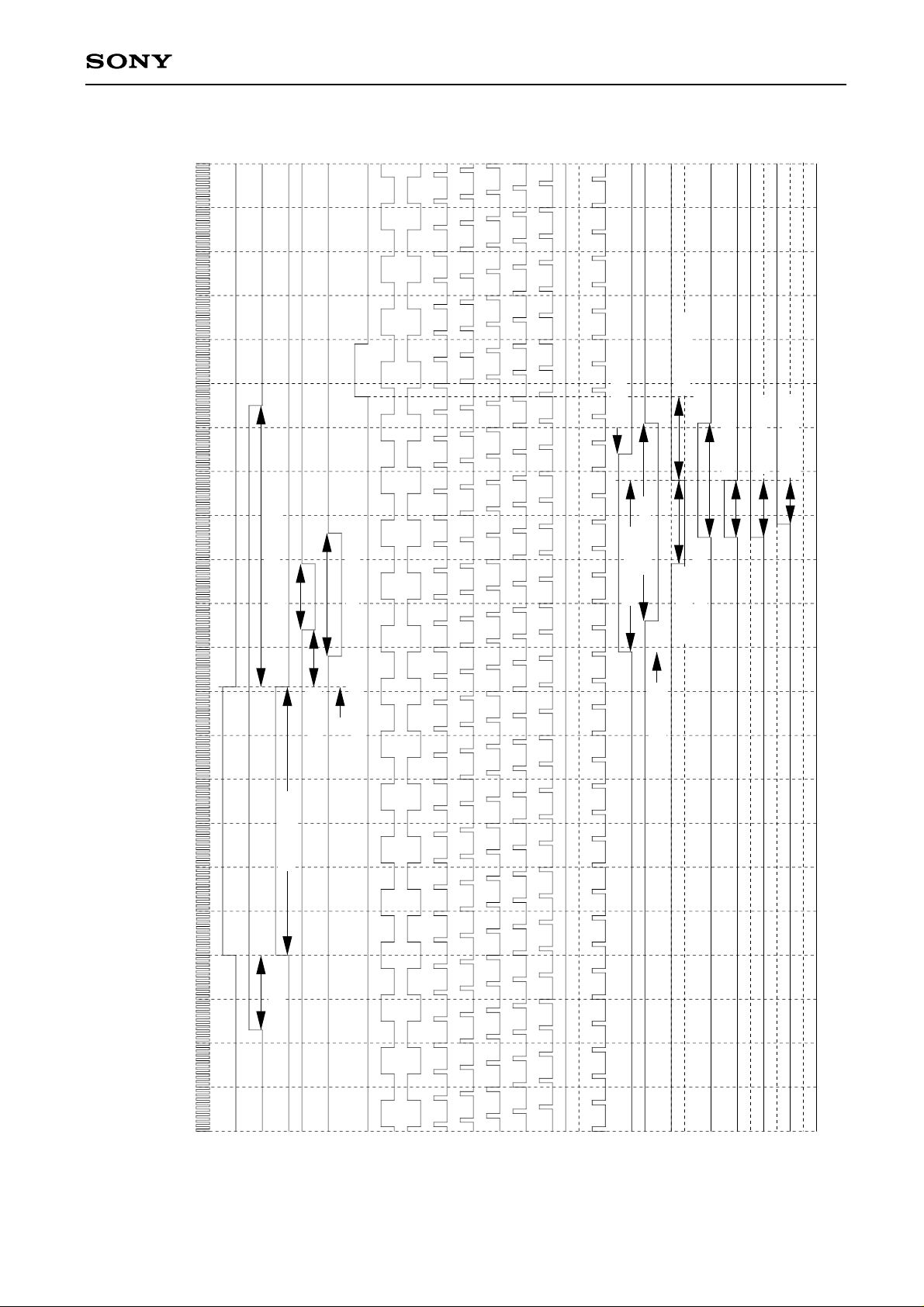
SLDWN: H (Down scan)
VP: 1100100 LSB
VD1IN
HD1IN
HDO
(BLK)
VST1
VCK
Vertical Direction Timing Chart (IBM-VGA 640 x 480)
—19—
FRP
(1H inversed)
HST
INT
ENB
CLR
FRP
(1F inversed)
VDO
(Internal reset)
VRST
Page 20
46
40
30
20
10
CXD2436Q
1
480
470
462
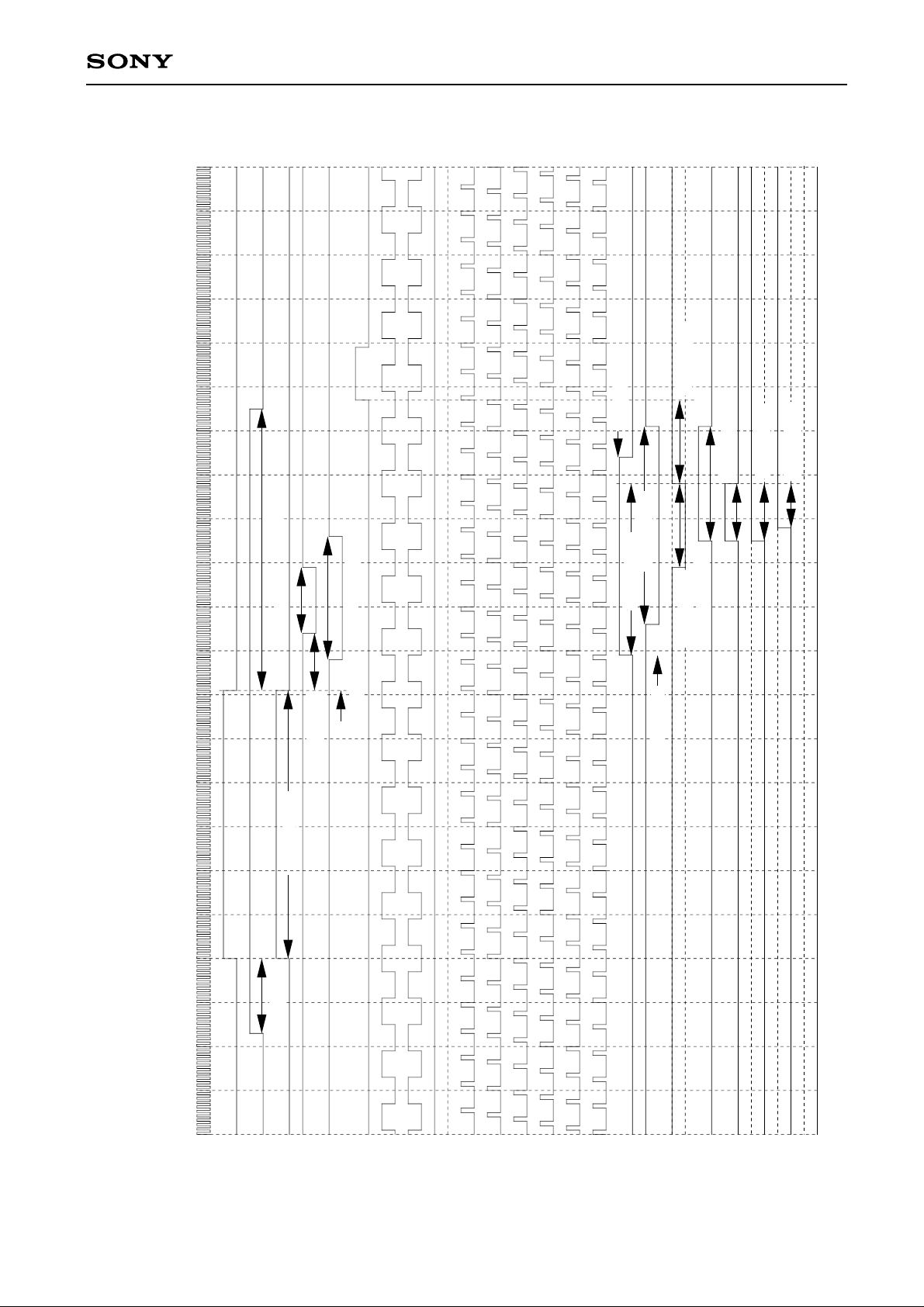
SLDWN: L (Up scan)
VP: 1100100 LSB
VD1IN
HD1IN
HDO
(BLK)
VST1
VCK
Vertical Direction Timing Chart (IBM-VGA 640 x 480)
—20—
(1H inversed)
FRP
HST
INT
ENB
CLR
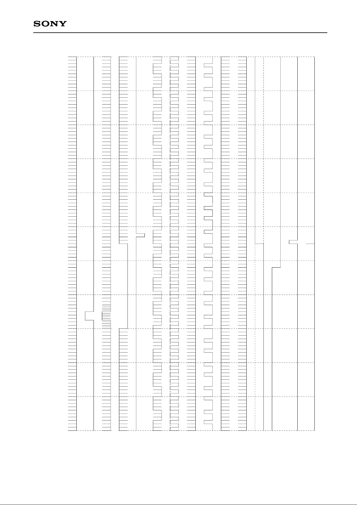
(1F inversed)
FRP
VDO
(Internal reset)
VRST
Page 21
MCK: 12.84 MHz (77.89 ns)
Loop Counter: 816 fh
µs (6fh)
0.47
µs (19fh)
1.48
µs (13fh)1.01
CXD2436Q
µs (10fh)
µs (13fh)1.01
0.78
µs (64fh)
4.98
µs (15fh)
1.17
µs (61fh)
4.75
µs (13fh)
1.01
µs (28fh)
2.18
µs (7fh)0.55
µs (45fh)
3.51
µs (39fh)
3.04
0.55µs (7fh)
µs (26fh)
2.03
µs (19fh)
1.48
µs (17fh)
1.32
776 786 796 806 0 10 20 30 40 50 60 70 80 90 100 110 120 130 140 150 160 170 180
RGT: H (Normal scan)
HP: 1000000 LSB CLPP: 10 LSB SHP: 0000 LSB
MCK
Horizontal Direction Timing Chart (NTSC)
CSYNC
(BLK)
/HD2IN
HDO
XCLP1
HST
XCLP2
HCK1
HCK2
SH2
SH1
—21—
SH3
SH4
SH5
SH6
SH7
CLR
ENB
VCK
PRG
PCG
FRP
VST1
INT
Page 22
MCK: 12.84 MHz (77.89 ns)
Loop Counter: 816 fh
0.47µs (6fh)
1.48µs (19fh)
1.01µs (13fh)
CXD2436Q
0.78µs (10fh)
1.01µs (13fh)
µs (64fh)
4.98
1.17µs (15fh)
4.75µs (61fh)
1.01µs (7fh)
2.18µs (28fh)
0.55µs (7fh)
3.51µs (45fh)
3.04µs (39fh)
0.55µs (7fh)
2.03µs (26fh)
1.48µs (19fh)
1.32µs (17fh)
RGT: L (Reverse scan)
Horizontal Direction Timing Chart (NTSC)
776 786 796 806 0 10 20 30 40 50 60 70 80 90 100 110 120 130 140 150 160 170 180
HP: 1000000 LSB CLPP: 10 LSB SHP: 0000 LSB
MCK
CSYNC
/HD2IN
(BLK)
HDO
XCLP1
HST
XCLP2
HCK1
HCK2
SH2
SH1
—22—
SH3
SH4
SH5
SH6
SH7
CLR
ENB
VCK
PRG
PCG
FRP
VST1
INT
Page 23
60
50
40
30
20
CXD2436Q
10
1
243
240
230
214 220
SLDWN: H (Down scan)
VP: 1111010 LSB
VCK
HD2IN
VD2IN
Vertical Direction Timing Chart (NTSC, odd field)
CSYNC
(BLK)
VST1
—23—
(1H inversed)
FRP
HST
INT
ENB
CLR
(1F inversed)
FRP
FLD
VDO
(Internal reset)
VRST
Page 24
60
50
40
30
20
CXD2436Q
10
1
243
240
230
220
213
SLDWN: H (Down scan)
VP: 1111010 LSB
VCK
CSYNC
(BLK)
VD2IN
Vertical Direction Timing Chart (NTSC, even field)
HD2IN
VST1
FRP
—24—
HST
(1H inversed)
INT
ENB
CLR
(1F inversed)
FRP
FLD
VDO
(Internal reset)
VRST
Page 25
60
50
40
30
20
CXD2436Q
10
1
243
240
230
214 220
SLDWN: L (Up scan)
VP: 1111010 LSB
HD2IN
Vertical Direction Timing Chart (NTSC, odd field)
VD2IN
CSYNC
(BLK)
VST1
VCK
—25—
(1H inversed)
FRP
HST
INT
ENB
CLR
(1F inversed)
FRP
FLD
VDO
(Internal reset)
VRST
Page 26
60
50
40
30
20
CXD2436Q
10
1
243
240
230
220
214
SLDWN: L (Up scan)
VP: 1111010 LSB
VCK
HD2IN
VD2IN
CSYNC
(BLK)
Vertical Direction Timing Chart (NTSC, even field)
VST1
FRP
—26—
HST
(1H inversed)
INT
ENB
CLR
(1F inversed)
FRP
FLD
VDO
(Internal reset)
VRST
Page 27
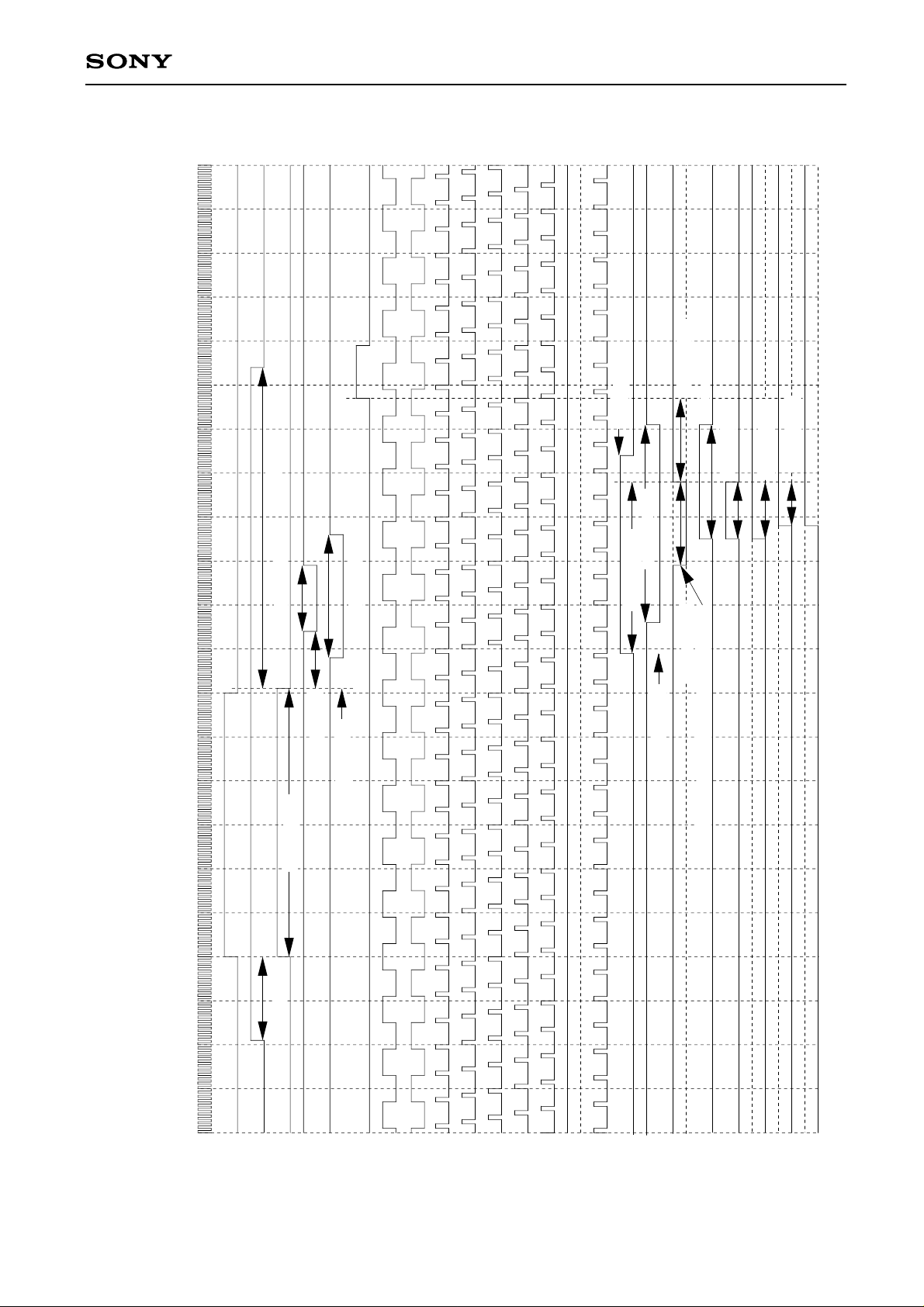
MCK: 12.75 MHz (78.43 ns)
Loop Counter: 816 fh
µs (73fh)
5.73
µs (6fh)
0.47
µs (45fh)
µs (19fh)
1.49
µs (26fh)
2.04
µs (13fh)
1.02
CXD2436Q
µs (10fh)
µs (13fh)1.02
0.78
µs (15fh)
1.18
µs (61fh)
4.78
µs (19fh)
1.49
µs (13fh)
1.02
µs (28fh)
2.20
µs (7fh)
0.55
3.53
µs (39fh)
3.06
µs (19fh)
1.49
µs (7fh)
0.55
VCK inversion timing for the decimation cycle
SLRGT: H (Normal scan)
HP: 1000000 LSB CLPP: 10 LSB SHP: 0000 LSB
Horizontal Direction Timing Chart (PAL)
776 786 796 806 0 10 20 30 40 50 60 70 80 90 100 110 120 130 140 150 160 170 180
MCK
/HD2IN
CSYNC
(BLK)
HDO
XCLP1
HST
XCLP2
HCK1
HCK2
SH2
SH1
—27—
SH3
SH4
SH5
SH6
SH7
CLR
ENB
VCK
PRG
PCG
FRP
VST1
INT
Page 28

MCK: 12.75 MHz (78.43 ns)
Loop Counter: 816fh
µs (73fh)
5.73
µs (15fh)
1.18
µs (28fh)
2.20
µs (6fh)
0.47
µs (39fh)
3.06
µs (45fh)
3.53
µs (19fh)
2.04
µs (26fh)
1.49
µs (19fh)
1.49
µs (13fh)1.02
CXD2436Q
µs (10fh)
µs (13fh)
0.78
1.02
µs (13fh)
µs (7fh)
1.02
0.55
µs (61fh)
4.78
0 10 20 30 40 50 60 70 80 90 100 110 120 130 140 150 160 170 180
µs (19fh)
1.49
SLRGT: L (Reverse scan)
Horizontal Direction Timing Chart (PAL)
776 786 796 806
HP: 1000000 LSB CLPP: 10 LSB SHP: 0000 LSB
MCK
SYNC
/HD2IN
(BLK)
HDO
XCLP1
HST
XCLP2
HCK1
HCK2
SH1
SH2
SH3
SH4
SH5
SH6
SH7
CLR
µs (7fh)
0.55
ENB
VCK inversion timing for the decimation cycle
VCK
PRG
PCG
FRP
VST1
INT
—28—
Page 29
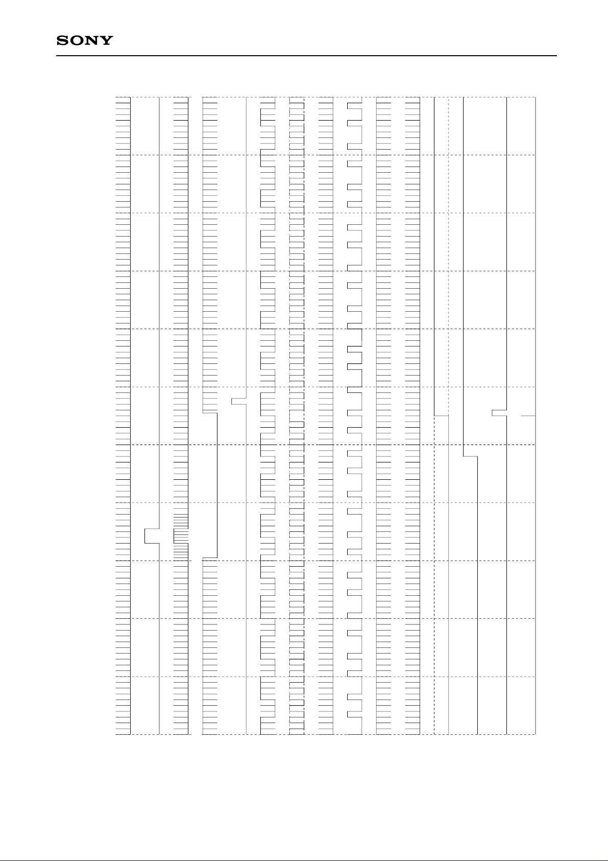
55
50
40
30
20
CXD2436Q
10
1
288
280
270
258260
SLDWN: H (Down scan)
VP: 1110010 LSB
VCK
HD2IN
VD2IN
CSYNC
(BLK)
VST1
Vertical Direction Timing Chart (PAL, odd field)
(1H inversed)
FRP
—29—
HST
INT
ENB
CLR
(1F inversed)
FRP
FLD
VDO
(Internal reset)
VRST
Page 30
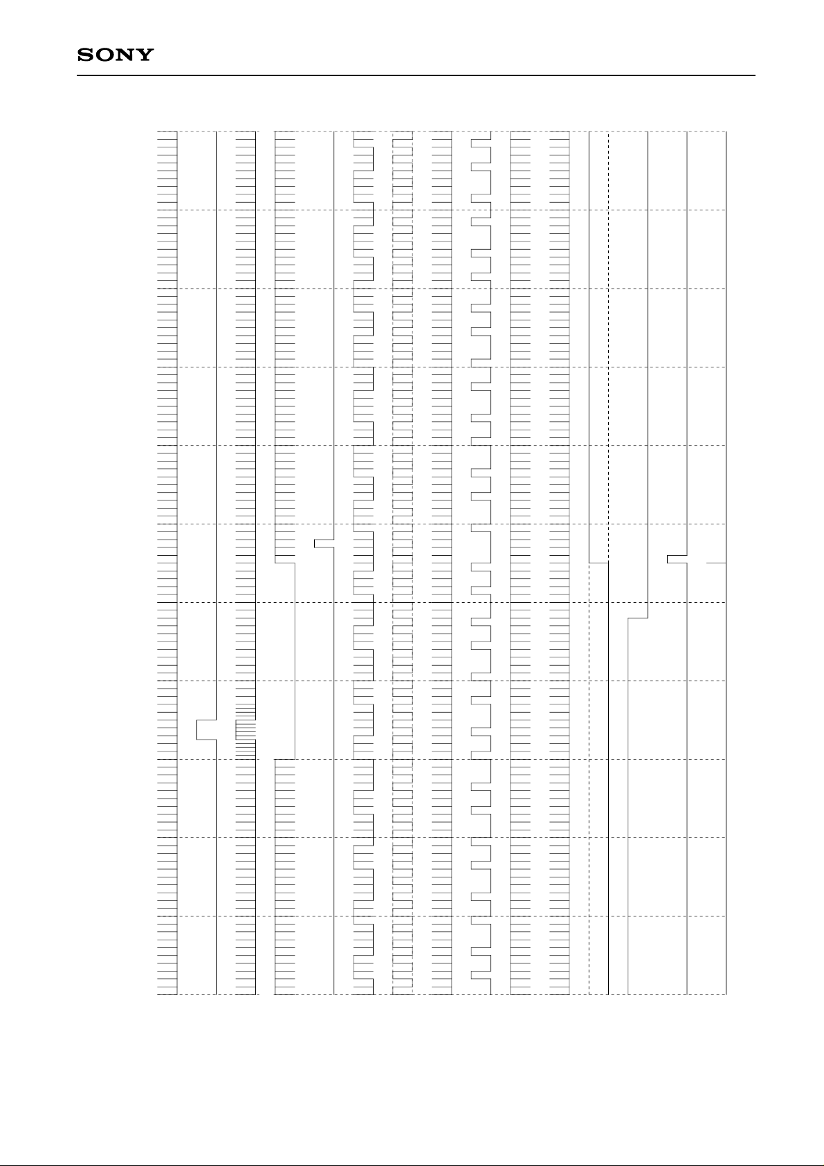
55
50
40
30
20
CXD2436Q
10
1
288
280
270
259
SLDWN: H (Down scan)
VP: 1110010 LSB
VCK
HD2IN
VD2IN
CSYNC
(BLK)
VST1
Vertical Direction Timing Chart (PAL, even field)
(1H inversed)
FRP
—30—
HST
INT
ENB
CLR
(1F inversed)
FRP
FLD
VDO
(Internal reset)
VRST
Page 31
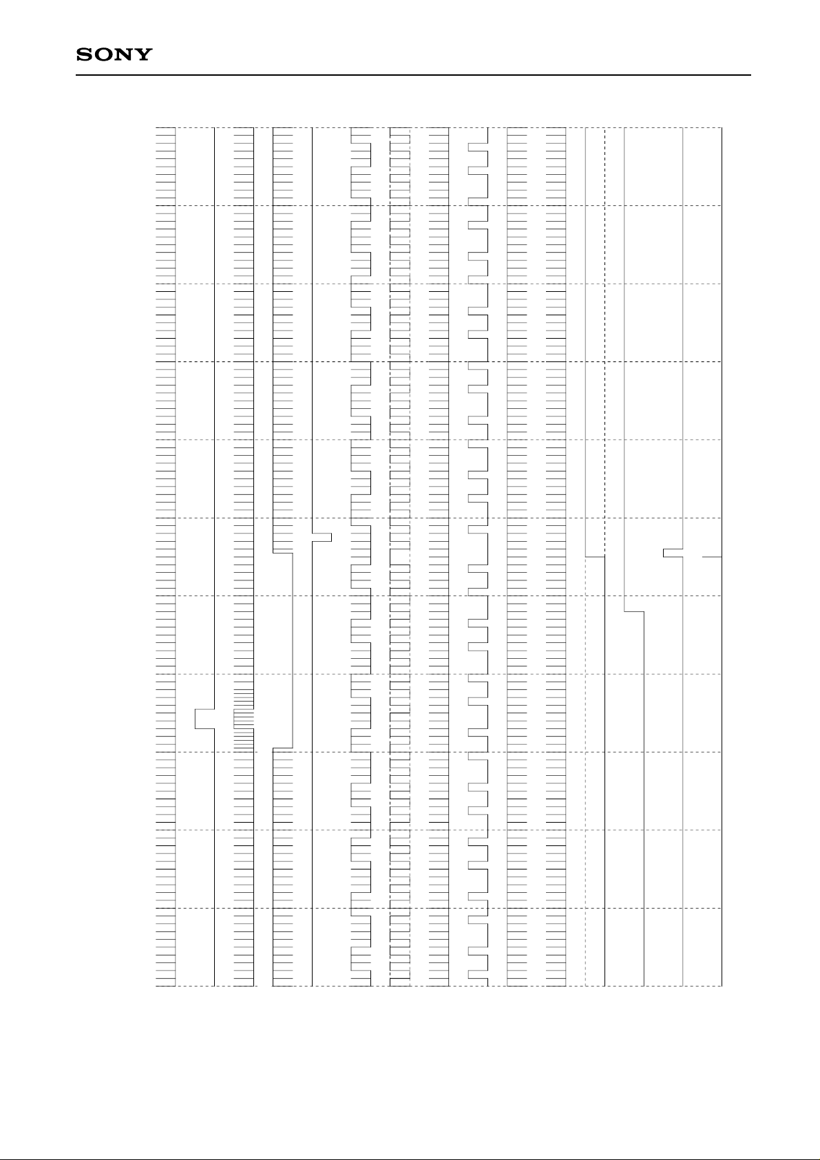
50
40
30
20
CXD2436Q
10
1
288
280
270
258
SLDWN: L (Up scan)
VP: 1110010 LSB
VCK
HD2IN
VD2IN
CSYNC
(BLK)
VST1
Vertical Direction Timing Chart (PAL, odd field)
(1H inversed)
FRP
—31—
HST
INT
ENB
CLR
(1F inversed)
FRP
FLD
VDO
(Internal reset)
VRST
Page 32
55
50
40
30
20
CXD2436Q
10
1
280
280
270
259
SLDWN: L (Up scan)
VP: 1110010 LSB
VCK
HD2IN
VD2IN
CSYNC
(BLK)
VST1
Vertical Direction Timing Chart (PAL, even field)
(1H inversed)
FRP
—32—
HST
INT
ENB
CLR
(1F inversed)
FRP
FLD
VDO
(Internal reset)
VRST
Page 33
CXD2436Q
1000p
0.1µ
31
PEO
SH7
100
33k
EXT-CKI
30
VSS
29
VDD
28
TST8
27
TST7
26
TST6
25
TST5
24
TST4
23
NC
22
TST3
TST2
SLMNB
SLSY
VD2IN
HD2IN
VSS
TST1
SLFR
SLRGT
SLDWN
VGAV
10 11 12 13 14 15 16 17 18 19 20 21
PLNT
XCLR
VPOL
HPOL
CSYNC
VSS
VDD
VD1IN
HD1IN
1 2 3 4 5 6 7 8 9
+5V
56p
1T363
0.01µ
10k
+12A
33k1k
33k
50k
3.3µ/
35V
0.01µ
3300p
3.3µ
/25V
10k
CKICSYNC
1HNOR
DOWNVGA
NT
POSI
POSI
GND
SLCKI
EXT-CKIHVD
SLSYSLFRSLRGTSLDWNVGAVPLNTHPOL VPOL
1FREV
UPAV
PAL
NEGA
NEGA
GND
0.1µ
47µ/16V
0.1µ
+5V
GND
GND GND
47µ
/16V
CLK
PLL IC
IN
FB IN
∗1. PLL IC
• Fall lock type
• VCO variable range: 20 to 35MHz
+5V
1µ
10k
+5V
0.01µ
6.8µ
47µ/16V
50k
100p
47
VSS
HST
84
GND
+5V
3-line serial input
45
46
VSS
VSS
HCK2
HCK1
86
85
CSSISCK
42
43
44
SI
CS
VSS
ENB
CLR
INT
89
88
87
1M
41
SCK
VSS
90
40
VSS
CXD2436QA
PCG
91
+5V
0.1µ
+5V
+5V
47µ/16V
0.1µ
47µ/16V
GND
48
49
50
VSS
VSS
TST10
VSS
5152535455565759 586061626364656667686970717273
VSS
VDD
VSS
PO0
PO1
PO2
PO3
PO4
PO5
PO6
PO7
PO8
PO9
VSS
PO10
PO11
HDN
XHDN
FLD
DWN
VDO
HDO
XHDO
74
PRG
75
XCLP1
7677787980
XCLP2
VDD
VSS
FRP
XFRP
RGT
XRGT
83
82
81
GND
39
TC
VCK
92
38
FP D
VST1
93
GND
1M
5.1k
32
33
34
35
36
37
CKI
CKO
RP D
SH3
96
SH4
97
SH5
98
PWM
SH6
99
TST 9
SH1
94
SL CKI
SH2
95
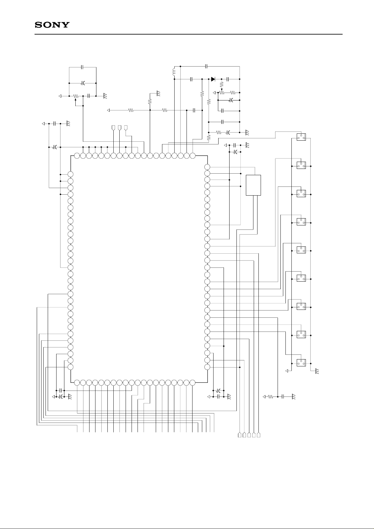
Application Circuit
to the panel
to the RGB driver
—33—
HD1 IN
VD1 IN
HD2 IN
CSYNC
VD2 IN
Application circuits shown are typical examples illustrating the operation of the devices. Sony cannot assume responsibility for
any problems arising out of the use of these circuits or for any infringement of third party and other right due to same.
Page 34
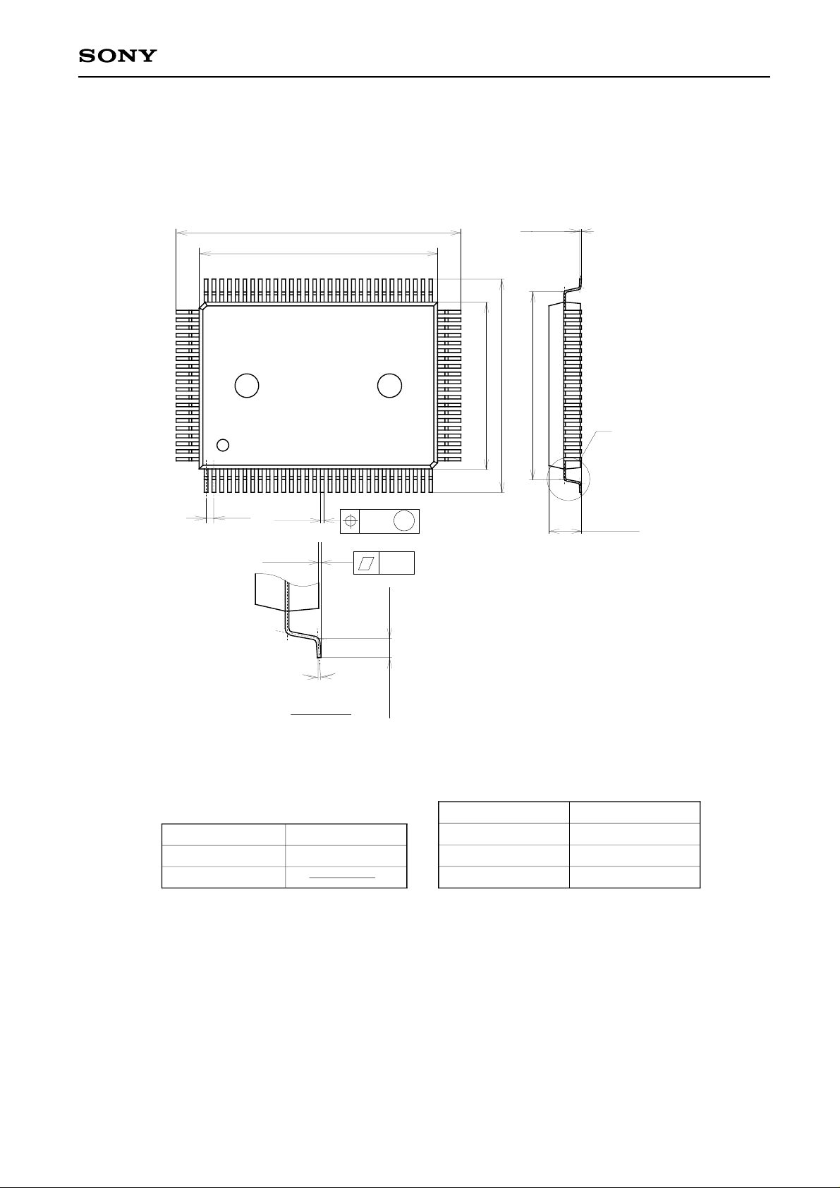
Package Outline Unit : mm
100PIN QFP (PLASTIC)
23.9 ± 0.4
+ 0.4
20.0 – 0.1
+ 0.4
17.9 ± 0.4
14.0 – 0.01
CXD2436Q
+ 0.1
0.15 – 0.05
15.8 ± 0.4
A
0.65
SONY CODE
EIAJ CODE
JEDEC CODE
0° to 15°
±0.12
DETAIL A
QFP-100P-L01
∗QFP100-P-1420-A
M
0.15
(16.3)
0.8 ± 0.2
2.75 – 0.15
PACKAGE STRUCTURE
PACKAGE MATERIAL
LEAD TREATMENT
LEAD MATERIAL
PACKAGE WEIGHT
EPOXY RESIN
SOLDER PLATING
COPPER / 42 ALLOY
1.4g
+ 0.35
—34—
 Loading...