

Page 1

—1—
E97841-TE
Sony reserves the right to change products and specifications without prior notice. This information does not convey any license by
any implication or otherwise under any patents or other right. Application circuits shown, if any, are typical examples illustrating the
operation of the devices. Sony cannot assume responsibility for any problems arising out of the use of these circuits.
Timing Generator for Progressive Scan CCD Image Sensor
48 pin TQFP (Plastic)
CXD2434ATQ
Absolute Maximum Ratings (Ta=25 °C)
• Supply voltage VDD VSS –0.5 to +7.0 V
• Input voltage VI VSS –0.5 to VDD +0.5 V
• Output voltage VO VSS –0.5 to VDD +0.5 V
• Operating temperature
Topr –20 to +75 °C
• Storage temperature
Tstg –55 to +150 °C
Recommended Operating Conditions
• Supply voltage VDD 4.75 to 5.25 V
• Operating temperature
Topr –20 to +75 °C
Description
The CXD2434ATQ is an IC developed to generate
the timing pulses required by the Progressive Scan
CCD image sensors as well as signal processing
circuits. The CXD2434ATQ adds EFS operation
when using the high-speed electronic shutter and
other changes to the CXD2434TQ specifications.
Features
• External trigger function
• Electronic shutter function
• Supports non-interlaced operation
• 30 frames/s
• Built-in driver for the horizontal (H) clock
• Base oscillation 1560 fH (24.5454 MHz)
Applications
Progressive Scan CCD cameras
Structure
Silicon gate CMOS IC
Applicable CCD Image Sensors
ICX084AK, ICX084AL
Page 2

—2—
CXD2434ATQ
TG
PULSE GENERATOR
10
13
14
21
18
22
23
17
16
19
38
39
40
REGISTER
PS
STRB
DCLK
DATA
SMD1
SMD2
XSUB
TEST1
TEST2
RESET
RG
H1
H2
XSHP
XSHD
XRS
XV1
XV2
XV3
XSG
CLD
CL
CKO
BUSY
WEN
ID
PBLK
XCPOB
XCPDM
VD
HD
STDBY
WM
SMDE
FSE
DECODE
COUNTER
GATE
41
48
28
11
9
8
7
5
4
3
252629424647313233343536
1 2
43 44 45
6
12 15 20 24 27 30 37
OSCO
OSCI
TRIG
ESG
EFS
V
SS
V
DD
V
SS
V
DD
V
SS
V
SS
V
DD
V
SS
1/2
1 2 3 4 5 6 7 8 9
10 11 12
13
14
15
16
17
18
19
20
21
22
23
24
35 34 33 32 31 30 29 28 27 252636
46
45
44
43
42
41
40
39
38
37
47
48
CXD2434ATQ
V
SS
CL
CLD
CKO
RESET
STDBY
TRIG
ESG
EFS
HD
VD
TEST2
V
SS
XRS
XSHD
XSHP
V
DD
XSG
XV1
XV2
XV3
V
SS
H2
H1
BUSY
WEN
ID
PBLK
XCPOB
SCPDM
V
DD
WM
TEST1
V
SS
SMDE
FSE
OSCO
OSCI
PS
STRB
DCLK
V
SS
DATA
SMD1
SMD2
RG
XSUB
V
DD
Block Diagram
Pin Configuration (Top View)
Page 3
—3—
CXD2434ATQ
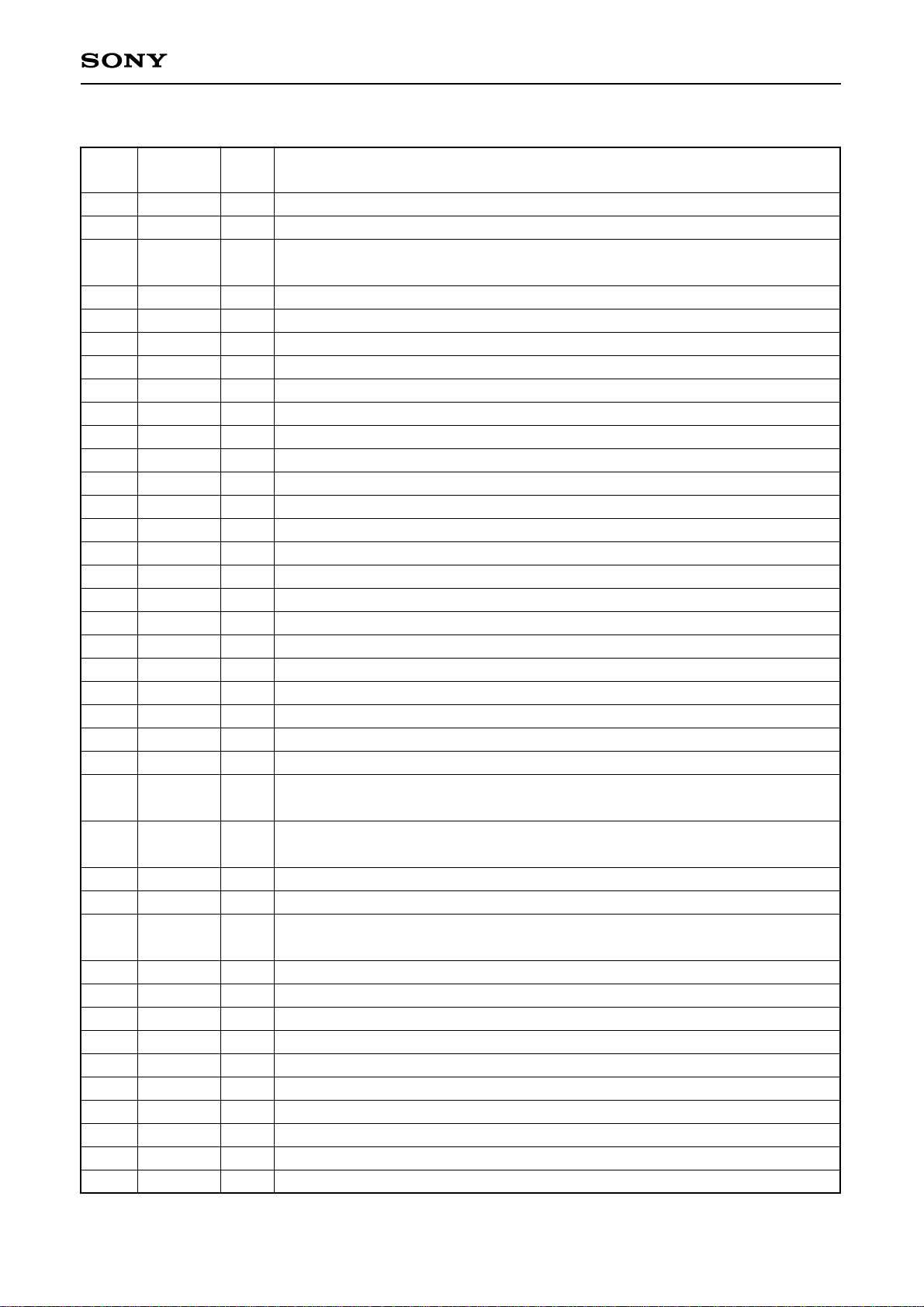
1
2
3
4
5
6
7
8
9
10
11
12
13
14
15
16
17
18
19
20
21
22
23
24
25
26
27
28
29
30
31
32
33
34
35
36
37
38
39
O
I
I
I
I
—
I
I
I
O
O
—
O
O
—
O
O
O
O
—
O
O
O
—
I
I
—
I
I
—
O
O
O
O
O
O
—
O
O
OSCO
OSCI
PS
STRB
DCLK
VSS
DATA
SMD1
SMD2
RG
XSUB
VDD
H1
H2
VSS
XV3
XV2
XV1
XSG
VDD
XSHP
XSHD
XRS
VSS
FSE
SMDE
VSS
TEST1
WM
VDD
XCPDM
XCPOB
PBLK
ID
WEN
BUSY
VSS
CL
CLD
Inverter output for oscillation.
Inverter input for oscillation.
Switching for electronic shutter speed input method. (With pull-up resistor)
Low: Serial input, High: Parallel input
Shutter speed setting. (With pull-up resistor)
Shutter speed setting. (With pull-up resistor)
GND
Shutter speed setting. (With pull-up resistor)
Shutter mode setting. (With pull-up resistor)
Shutter mode setting. (With pull-up resistor)
Reset gate pulse output.
CCD discharge pulse output.
Power supply.
Clock output for horizontal CCD drive.
Clock output for horizontal CCD drive.
GND
Clock output for vertical CCD drive.
Clock output for vertical CCD drive.
Clock output for vertical CCD drive.
Sensor charge readout pulse output.
Power supply.
Sample-and-hold pulse output.
Sample-and-hold pulse output.
Sample-and-hold pulse output.
GND
Switching for external trigger discharge operation. (With pull-up resistor)
Low: No high-speed discharge, High: High-speed discharge
Switching for readout timing. (With pull-up resistor)
Low: ESG input valid, High: ESG input invalid
GND
Test. (With pull-down resistor)
WEN mode setting. (With pull-down resistor)
Low: Effective line, High: XSG synchronization
Power supply.
Clamp pulse output.
Clamp pulse output.
Blanking cleaning pulse output.
Line identification output.
Write enable output.
Trigger mode flag output.
GND
780 fH clock output.
AD conversion pulse output.
Pin Description
Pin No. Symbol I/O Description
Page 4
—4—
CXD2434ATQ
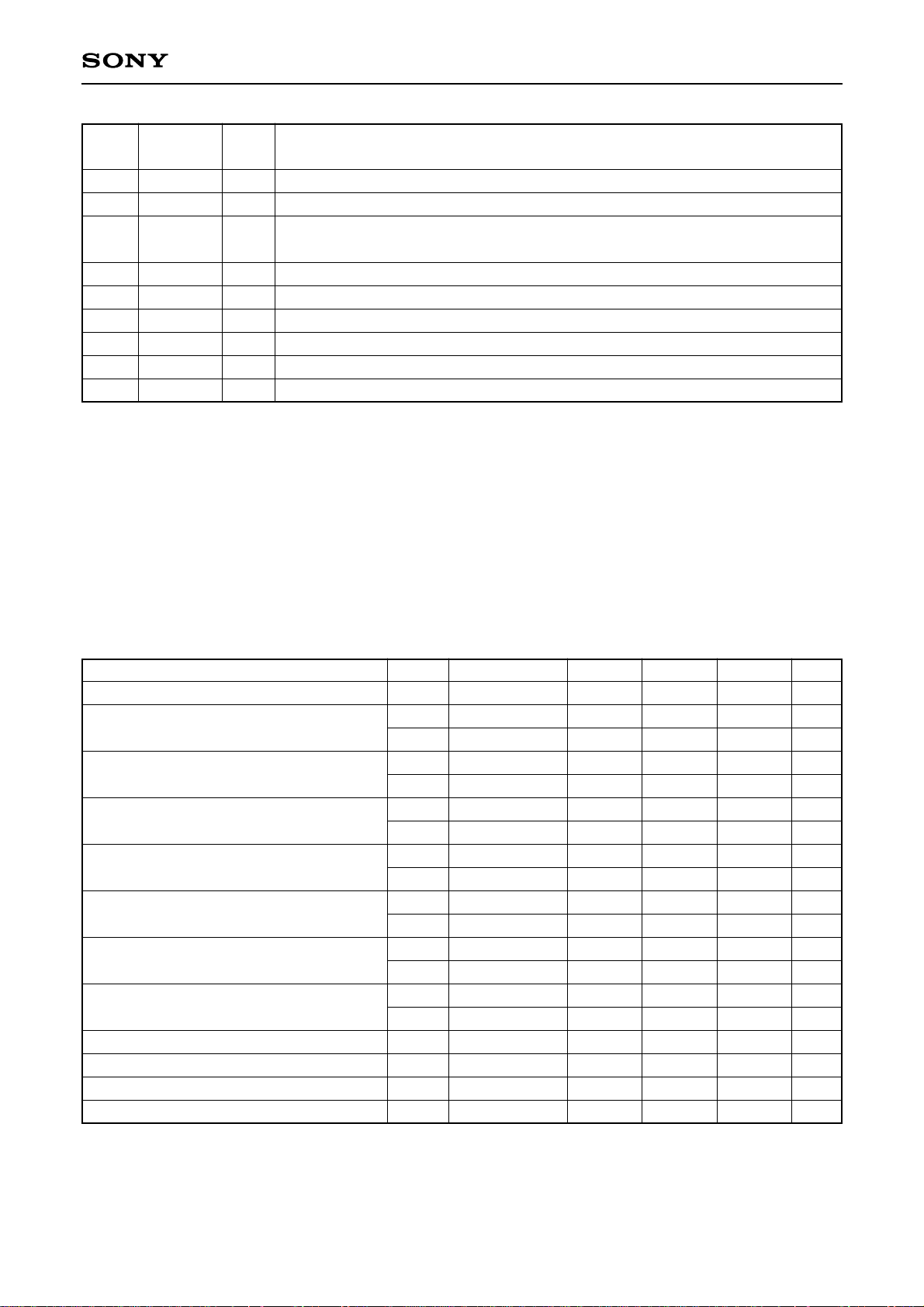
Pin No. Symbol I/O Description
40
41
42
43
44
45
46
47
48
CKO
RESET
STDBY
TRIG
ESG
EFS
HD
VD
TEST2
O
I
I
I
I
I
I
I
I
1560 fH clock output.
RESET. (With pull-up resistor) Low : Reset, High : Normal
Standby. (With pull-up resistor)
Low: Internal clock supply stopped, High: Normal
External trigger input. (With pull-up resistor)
External readout input. (With pull-up resistor)
Vertical CCD discharge input. (With pull-up resistor)
Horizontal sync signal input.
Vertical sync signal input.
Test. (With pull-up resistor)
Electrical Characteristics
1. DC Characteristics VDD=4.75 V to 5.25 V Topr= –20 to +75 °C
Item
Supply voltage
Input voltage 1
(Input pins other than those listed below)
Input voltage 2
(Pin 2)
Output voltage 1
(Output pins other than those listed below)
Output voltage 2
(Pins 21, 22, 23, 38, 39 and 40)
Output voltage 3
(Pin 10)
Output voltage 4
(Pins 13 and 14)
Output voltage 5
(Pin 1)
Feedback resistor
Pull-up resistor
Pull-down resistor
Current consumption
Symbol
VDD
VIH1
VIL1
VIH2
VIL2
VOH1
VOL1
VOH2
VOL2
VOH3
VOL3
VOH4
VOL4
VOH5
VOL5
RFB
RPU
RPD
IDD
Conditions
IOH=–2.5 mA
IOL=4.5 mA
IOH=–5.0 mA
IOL=9.0 mA
IOH=–7.5 mA
IOL=13.5 mA
IOH=–14.0 mA
IOL=24.0 mA
VIN=VSS or VDD
VIL=0 V
VIH=VDD
VDD=5 V
Min.
4.75
0.7 VDD
0.7 VDD
VDD–0.4
VDD–0.4
VDD–0.4
VDD–0.4
VDD/2
Typ.
5.0
1 M
50 k
50 k
40
Max.
5.25
0.3 VDD
0.3 VDD
0.4
0.4
0.4
0.4
VDD/2
100 k
100 k
Unit
V
V
V
V
V
V
V
V
V
V
V
V
V
V
V
Ω
Ω
Ω
mA
Page 5
—5—
CXD2434ATQ
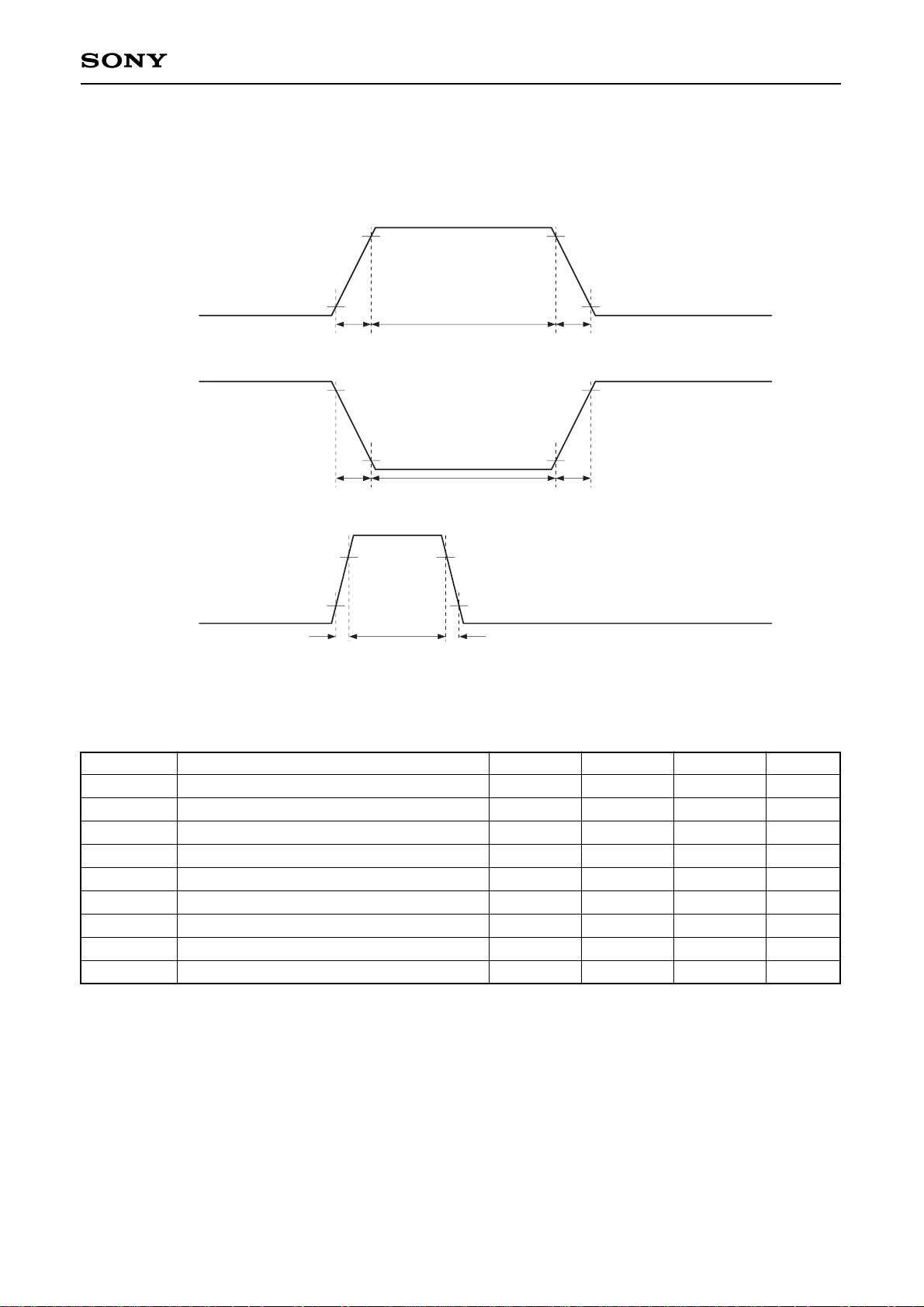
2. AC Characteristics
1) Waveform characteristics of H1, H2 and RG
tRH1 tWH1 tFH1
0.9VDD
0.1VDD
0.9VDD
0.1VDD
tFH2 tWH2 tRH2
tRRG tWRG tFRG
H1
H2
RG
0.9V
DD
0.1VDD
VDD=5.0 V, Topr=25 °C, load capacitance of H1 and H2=100 pF, load capacitance of RG=10 pF
Symbol
tRH1
tFH1
tWH1
tRH2
tFH2
tWH2
tRRG
tFRG
tWRG
Definition
H1 rise time
H1 fall time
H1 high level time
H2 rise time
H2 fall time
H2 low level time
RG rise time
RG fall time
RG high level time
Min.
25
25
10
Typ.
6
5
35
6
5
35
2
2
15
Max.
15
15
15
15
5
5
20
Unit
ns
ns
ns
ns
ns
ns
ns
ns
ns
Page 6

—6—
CXD2434ATQ
2) Phase characteristics of H1, H2, RG, XSHP, XSHD, XRS, CL, CLD and CKO
tH1
0.5VDD 0.5VDD 0.5VDD
tPD3 tPD1
0.5VDD 0.5VDD
tPD2
0.5VDD 0.5VDD
tPD4 tPD5
tW1
0.5VDD 0.5VDD
tW2 tPD6
0.5VDD 0.5VDD
0.5VDD
tPD7
0.5VDD
tPD8 tPD9
0.5VDD 0.5VDD
tW3tPD10
tW4
0.5VDD 0.5VDD
tW5
tW5
0.5VDD 0.5VDD
0.5VDD
0.5VDD
tPD11 tPD11
H1
H2
RG
XSHP
XSHD
XRS
CLD
CL
CLO
VDD=5.0 V, Topr=25 °C, load capacitance of CL and CKO=30 pF, load capacitance of CLD, XSHP, XSHD, XRS and RG=10 pF
Symbol
tH1
tPD1
tPD2
tPD3
tPD4
tPD5
tPD6
tPD7
tPD8
tPD9
tPD10
tPD11
tW1
tW2
tW3
tW4
tW5
Definition
H1 cycle
H2 rising delay, activated by the falling edge of H1
H2 falling delay, activated by the rising edge of H1
H1 rising delay, activated by the rising edge of RG
XSHP falling delay, activated by the falling edge of RG
H1 falling delay, activated by the rising edge of XSHP
H1 rising delay, activated by the rising edge of XSHD
CLD falling delay, activated by the falling edge of XSHD
CLD falling delay, activated by the rising edge of XRS
XRS falling delay, activated by the falling edge of CLD
CL falling delay, activated by the rising edge of H1
H1 rising (falling) delay, activated by the rising edge of CKO
XSHP pulse width
XSHD pulse width
CLD pulse width
CL pulse width
CKO pulse width
Min.
–5
–5
–5
–2
–7
–5
–5
17
0
–5
–5
13
15
17
38
17
Typ.
82
0
0
0
4
2
2
2
22
8
0
2
18
20
22
41
20
Max.
5
5
5
10
7
7
7
27
15
5
7
23
25
27
45
24
Unit
ns
ns
ns
ns
ns
ns
ns
ns
ns
ns
ns
ns
ns
ns
ns
ns
ns
Page 7
—7—
CXD2434ATQ
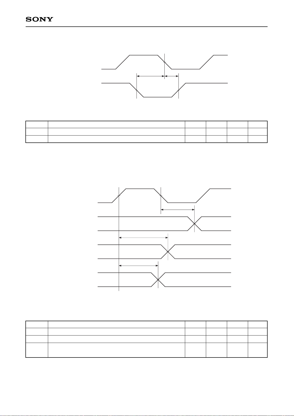
3) Phase conditions of HD, VD, TRIG, EFS and ESG
0.5VDD
tSETUP
tHOLD
0.5VDD 0.5VDD
CL
HD, VD, TRIG
EFS, ESG
VDD=5.0 V, Topr=25 °C, load capacitance of CL=30 pF
Symbol
tSETUP
tHOLD
Definition
HD, VD, TRIG, EFS and ESG setup time, activated by CL
HD, VD, TRIG, EFS and ESG hold time, activated by CL
Min.
20
5
Typ. Max. Unit
ns
ns
4) Phase characteristics of XV1, XV2, XV3, XSG, PBLK, XCPDM, XCPOB, BUSY, WEN and ID
0.5VDD 0.5VDD
tPDCL1
0.5VDD
tPDCL2
0.5VDD
tPDCL3
0.5VDD
CL
XV1, XV2, XV3
BUSY, WEN, ID
XSG, PBLK,
XCPDM, XCPOB
VDD=5.0 V, Topr=25 °C, load capacitance of CL=30 pF,
load capacitance of XV1, XV2, XV3, XSG, PBLK, XCPDM, XCPOB, BUSY, WEN and ID=10 pF
Symbol
tPDCL1
tPDCL2
tPDCL3
Definition
XV1, XV2 and XV3 delay, activated by the falling edge of CL
BUSY, WEN and ID delay, activated by the rising edge of CL
XSG, PBLK, XCPDM and XCPOB delay, activated by the
rising edge of CL
Min.
30
40
40
Typ. Max.
65
60
55
Unit
ns
ns
ns
Page 8
—8—
CXD2434ATQ
Description of Functions
1. Progressive Scan CCD drive pulse generation
• Combining this IC with a crystal oscillator generates a fundamental frequency of 24.5454 MHz.
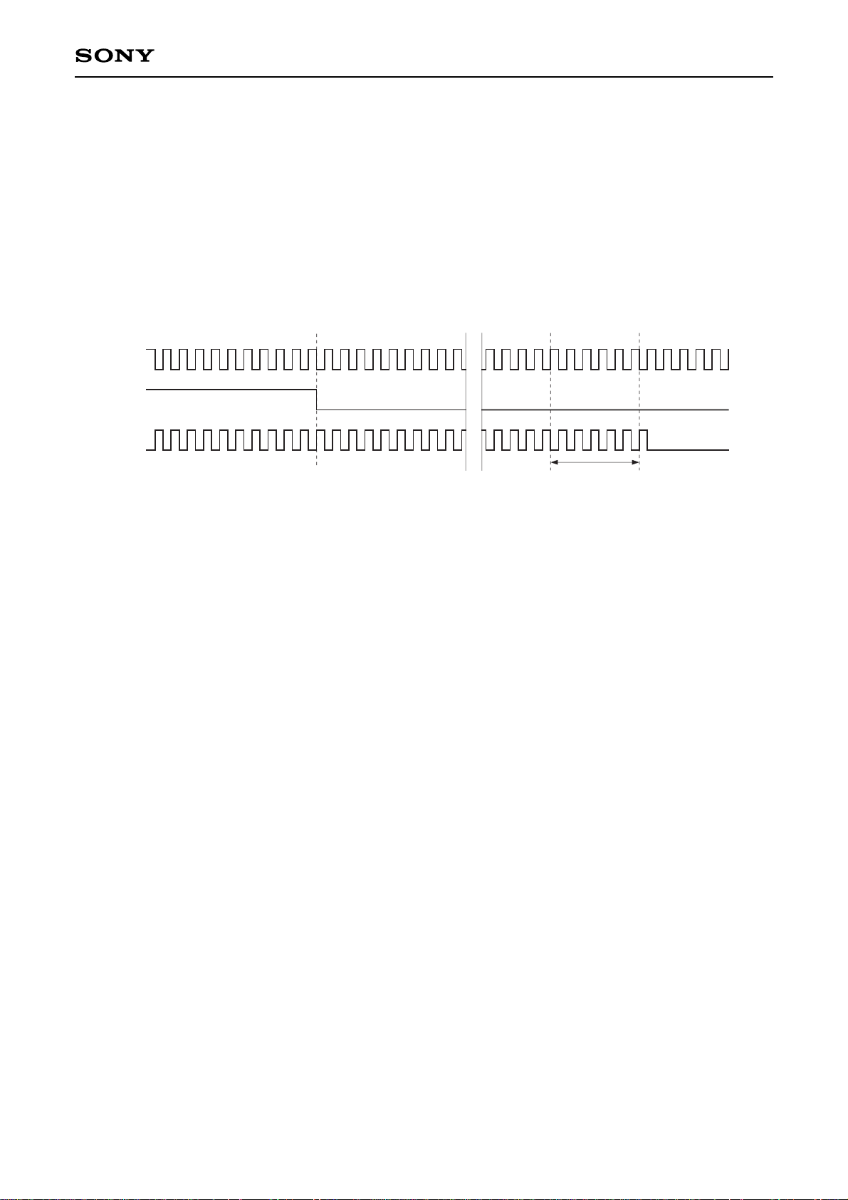
• CCD drive pulse generation is synchronized with the HD and VD inputs.
Set fCL to 780 fHD and fHD to 525 fVD.
• The various operations are performed by the TRIG, EFS and ESG inputs. (See the following items.)
<Detection timing for VD, TRIG, EFS and ESG>
35
T1
1
CL
HD
H1
Detection timing for VD,
TRIG, EFS and ESG
After HD input is detected, the status of VD, TRIG, ESG and EFS is detected during T1.
Do not change the status of VD, TRIG, ESG and EFS during T1.
When input is from a non-synchronized system, the low level period for each pulse should be set to 63.5 µs
or longer to prevent misoperation.
2. Reset
The internal register values are undetermined immediately after power-on, so perform one of the following
reset operations.
1. Reset by the RESET pin
Reset is performed by setting the RESET pin low for a period of 80 ns or more. Reset can also be
performed by setting the RESET pin low during power-on and then switching the RESET pin from low to
high when VDD rises to 4.75 V or higher. Note that when reset is performed by the RESET pin, the
electronic shutter settings made by serial input are also reset.
2. Reset by turning off the electronic shutter
Reset is performed by setting the shutter mode to electronic shutter off and inputting VD. Note that in
this case the TRIG, ESG and EFS pins should all be set high.
Page 9
—9—
CXD2434ATQ
3. Electronic shutter
<Shutter modes>
The electronic shutter has the following four shutter modes.
• Electronic shutter off : Exposure time is 1/30 s.
• High-speed electronic shutter : Exposure time is shorter than 1/30 s.
• Low-speed electronic shutter: Exposure time is longer than 1/30 s.
• Flickerless : Exposure time is 1/50 s. This is a special feature of the high-speed
electronic shutter, and reduces flicker from fluorescent lights, etc. in areas
with 50 Hz power supply
<Shutter mode and speed setting methods>
PS=Low : Serial input; set by the STRB, DCLK and DATA pins. The SMD1 and SMD2 pins are not used.
PS=High : Parallel input; set by the STRB, DCLK, DATA, SMD1 and SMD2 pins.
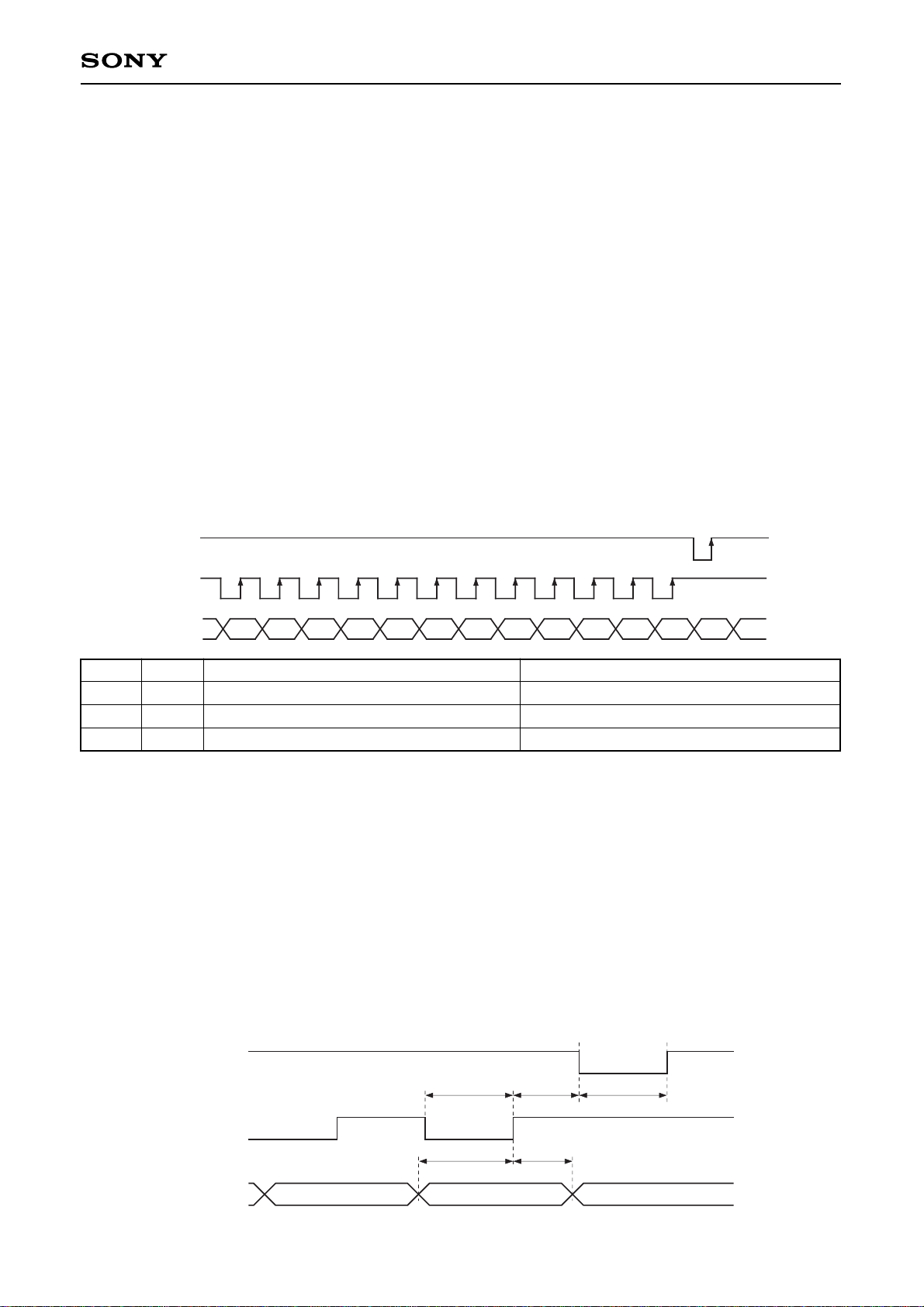
3-1. [Serial input]
Serial input is set by the STRB, DCLK and DATA pins. The electronic shutter mode and the meanings of the
numbers indicated by D0 to 9 vary according to the SMD1 and SMD2 setting of the internal register.
STRB
DCLK
DATA
SMD2 SMD1 D9 D8 D7 D6 D5 D4 D3 D2 D1 D0
SMD1
H
L
H
SMD2
H
H
L
Mode
Electronic shutter off (1/30 s accumulation)
High-speed electronic shutter
Low-speed electronic shutter
D0 to 9
—
Number of exposed lines (Note 1)
Number of exposed frames (Note 2)
Note 1) Relationship between the number of exposed lines and the exposure time
The relationship between the number of exposed lines and the exposure time is as follows.
(Exposure time)=(Number of exposed lines) × (One horizontal scan period) + (Accumulation time for
the readout lines)
In this formula, one horizontal scan period equals the HD falling interval, and the accumulation time for
the readout lines is the time from the rising edge of XSUB to the rising edge of XSG (456 bits). Also,
(Number of exposed lines) should be set to greater than 1 but less than 524.
Note 2) The number of exposed frames should be set to greater than 1 but less than 1023. However, when
the number of exposed frames is 1 and SMDE is set to high, external trigger mode does not function.
tWD tSDS tWS
tSDD tHDD
STRB
DCLK
DATA
Timing Chart (Serial input)
Page 10
—10—
CXD2434ATQ
AC characteristics for serial input
Symbol
tSDD
tHDD
tSDS
tWS
tWD
Definition
DATA setup time, activated by the rising edge of DCLK
DATA hold time, activated by the rising edge of DCLK
DCLK setup time, activated by the falling edge of STRB
STRB pulse width
DCLK pulse width
Min.
10 ns
10 ns
10 ns
82 ns
82 ns
Max.
—
—
—
—
—
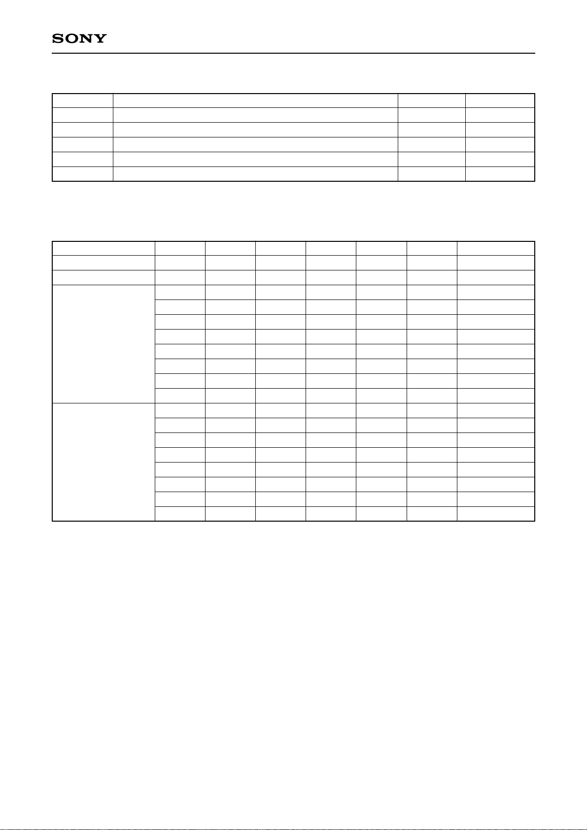
3-2. [Parallel input]
Mode
Electronic shutter off
Flickerless
High-speed shutter
Low-speed shutter
PS
H
H
H
H
H
H
H
H
H
H
H
H
H
H
H
H
H
H
SMD1
H
L
L
L
L
L
L
L
L
L
H
H
H
H
H
H
H
H
SMD2
H
L
H
H
H
H
H
H
H
H
L
L
L
L
L
L
L
L
STRB
X
X
H
L
H
L
H
L
H
L
H
L
H
L
H
L
H
L
DCLK
X
X
H
H
L
L
H
H
L
L
H
H
L
L
H
H
L
L
DATA
X
X
H
H
H
H
L
L
L
L
H
H
H
H
L
L
L
L
Exposure time
1/30 s
1/50 s
1/60 s
1/125 s
1/250 s
1/500 s
1/1000 s
1/2000 s
1/4000 s
1/10000 s
2 FRM
3 FRM
4 FRM
5 FRM
6 FRM
7 FRM
8 FRM
9 FRM
Page 11

—11—
CXD2434ATQ
4. External trigger mode
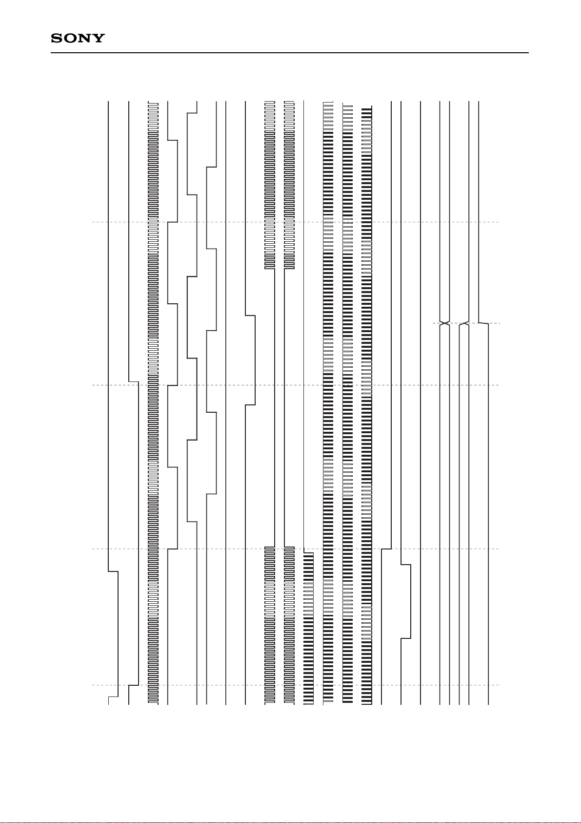
External trigger mode starts exposure in sync with the external trigger input. No special pins are required to
set this mode.
The IC prepares to shift to external trigger mode with the falling edge of the TRIG pin (Note). The timing to
shift to external trigger mode varies according to the mode setting. (See the table.) The BUSY pin
maintains high status during external trigger mode. Whether or not to discharge the vertical CCD charge is
set by FSE.
Note) See the detection timing for VD, TRIG, EFS and ESG.
Mode settings during external trigger (Note 1)
PS
L
H
H
X
X
SMD1
L
L
L
H
H
SMD2
X
H
L
L
H
Description of operation
The IC is shifted to external trigger mode by HD, exposure is finished after the set
time, and XSG is output. (Note 2) (Note 3)
The IC is shifted to external trigger mode by HD, exposure is finished 1/50 s later,
and XSG is output.
Do not set for external trigger.
Trigger input is not accepted.
Note 1) The SMD1 and SMD2 setting method varies according to the PS status. See “3. Electronic shutter”.
PS=Low : Set by serial input.
PS=High : Set by the SMD1 and SMD2 pins.
Note 2) The exposure time setting method is the same as the exposure time setting for the electronic shutter.
Note 3) When FSE=high, set the number of exposed lines from 1 to 522.
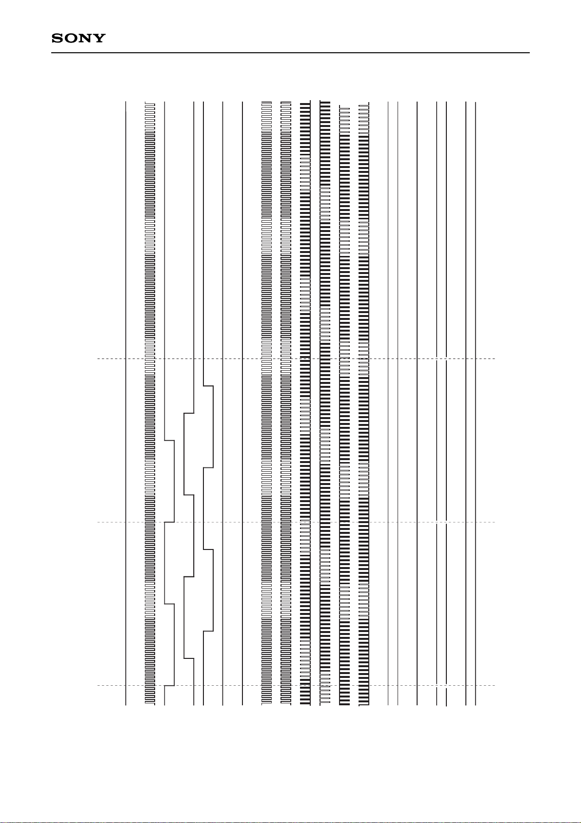
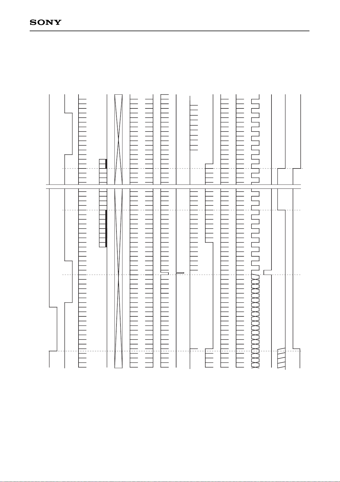
<FSE and discharge operation>
During external trigger mode, the previously exposed signal charge sometimes remains in the vertical CCD
when exposure finishes. In this case, the image shot with external trigger mode is output overlapped with
the previously shot image. Setting FSE to high performs discharge operation for signal charges remaining
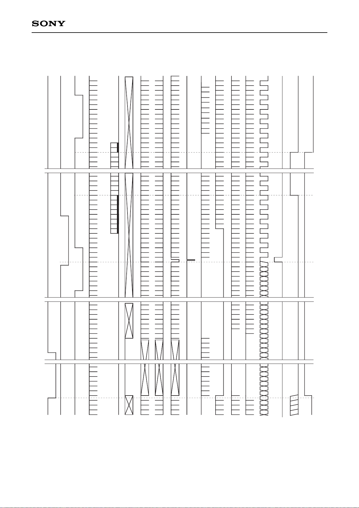
in the vertical CCD after trigger input. Discharge operation is not performed when FSE is low. This setting
is only valid when SMD1 is low.
<Finishing the exposure period with ESG>
During external trigger mode, exposure can be finished in sync with the falling edge of ESG (Note). If
SMDE is set to low, the XSG pulse is output regardless of the electronic shutter setting, when the falling
edge of ESG is detected. ESG should be fixed to high status at all times other than during external trigger
mode. Do not change SMDE while BUSY is high.
Note) See the detection timing for VD, TRIG, EFS and ESG.
<Signal after external trigger mode>
After high-speed external trigger mode is finished, the exposure time differs from that performed by the
electronic shutter setting. This is because the start and finish of external trigger mode are not synchronized
to VD input.
Page 12
—12—
CXD2434ATQ
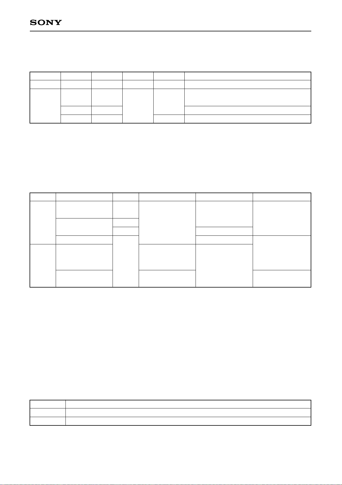
5. Discharge of the vertical CCD
During EFS is low, discharge of the vertical CCD is performed. During FSE is high in the external trigger
mode, the vertical control line by line is possible. That is different from discharge operation. The falling in
the effective interval of EFS is detected, discharge is not performed even if the low status is held until the
next effective period. For frames using EFS, set electronic shutter off or high-speed electronic shutter.
When EFS is used, WEN (WM=low) may not indicate the proper status.
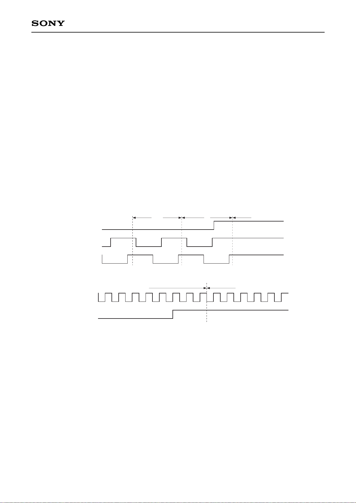
<Discharge start>
Vertical CCD discharge is started in sync with HD input after the falling edge of EFS (Note). Approximately
3420 ns (81.4 ns × 42 clock pulses) are required to transfer one line vertically.
Note) See the detection timing for VD, TRIG, EFS and ESG.
<Discharge finish>
Since the operation uses 42 clock pulses as one unit, when the rising edge of EFS is detected in interval
[n], discharge operation stops from interval [n+1]. The period from the rising edge of EFS to the falling
edge of VD must be longer than 2HD.
n–1 n n+1
EFS
XV1
XV3
Timing Chart 1
Timing Chart 2
CL
XV3
n n+1
<Maximum number of dischargeable lines>
The number of lines transferred by discharge transfer and normal transfer during the following period
should not exceed 4096 lines.
Period : The period from when the XSG pin becomes low until XSG becomes low again or the TRIG pin
becomes low.
6. Internal logic stop (standby mode)
When the STDBY pin is set to low, clock supply is stopped to a part of the internal logic. However, output
from the oscillation cell (OSCI and OSCO pins) as well as the CL and CKO pins does not stop. The status
of each output pin when STDBY is low is shown below.
High : XSUB, XSG
Low : RG, H1, H2, XV1, XV2, XV3, XSHP, XSHD, XRS, XCPOB, XCPDM, PBLK, ID, WEN,
BUSY, CLD
Not stopped : OSCO, CL, CKO
Page 13
—13—
CXD2434ATQ
7. Mode settings
7-1. VD input-related
Note 1) When PS is high, SMD1 and SMD2 indicate the status of the SMD1 and SMD2 pins, respectively.
When PS is low, these are the corresponding internal register values. See “3. Electronic shutter”.
Note 2) Operation when PS=high, SMD1=low and SMD2=low conforms to that when SMD1=low and
SMD2=high.
7-2. TRIG, ESG and EFS input-related
BUSY
H
L
SMDE
X
H
L
X
Discharge period
(Note 1)
Exposure period
Signal output period
Before TRIG input
After TRIG input
(Note 2) (Note 3)
TRIG
Prohibited
IC shifted to
external trigger
mode (Note 3)
Prohibited
ESG
Prohibited
Readout operation (Note 4)
Prohibited
Prohibited (Note 5)
EFS
Invalid
Discharge operation
(Note 6) (Note 7)
Prohibited
Note 1) Only when FSE is high.
Note 2) Valid only during low-speed shutter.
Note 3) See “4. External trigger mode”.
Note 4) ESG input is valid only one time after TRIG input. Do not input ESG two times or more.
Note 5) Fix ESG to high status when BUSY is low.
Note 6) When EFS is low, readout is not activated by VD input. See “7-1. VD input-related”.
Note 7) Use in electronic shutter off state.
Note 8) In case any two pins or more among TRIG, ESG, and EFS are falled at the same time, the operation is
not guaranteed.
7-3. WEN mode switching by WM
WM
L
H
Description of WEN operation
Lines for which the signal from the CCD is valid output high; all other lines output low.
Output is synchronized with XSG.
BUSY
H
L
SMD1
L
H
X
X
SMD2
H
L
H
X
SMDE
X
X
EFS
X
H
L
VD input
Invalid
Readout operation or the number of
accumulated frames is counted.
Readout operation is performed.
Invalid
Page 14

—14—
CXD2434ATQ
Application Circuit
+5V
CXD2434ATQ
CXD2311AR
CXA2006Q
ICX084AK/AL
CXD1267AN
+15V
100k
1000p
12
11
10
9
8
7
6
5
4
3
2
1
13
14
15
16
17
18
19
20
21
22
23
24
35
34
33
32
31
30
29
28
27
26
25
36
46
45
44
43
42
41
40
39
38
47
37
48
Reset Circuit
Application circuits shown are typical examples illustrating the operation of the devices. Sony cannot assume responsibility for
any problems arising out of the use of these circuits or for any infringement of third party patent and other right due to same.
Page 15
—15—
CXD2434ATQ
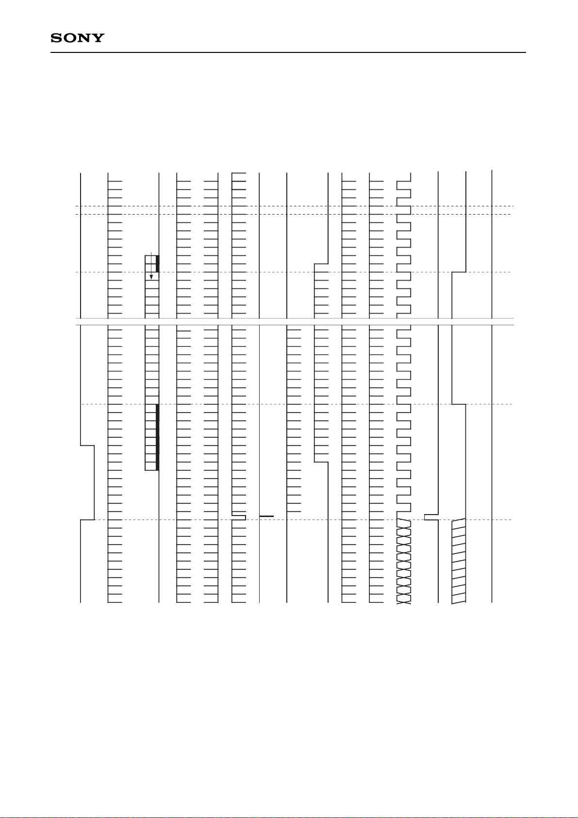
Normal Operation (vertical synchronization)
1
14
508
510
1 2 3 4 5 6 7 8 1 2 3 4
494
VD
HD
OUT
XV1
XV2
XV3
XSG
XSUB
PBLK
XCPOB
XCPDM
ID
WEN
(WM=High)
WEN
(WM=Low)
BUSY
Page 16
—16—
CXD2434ATQ
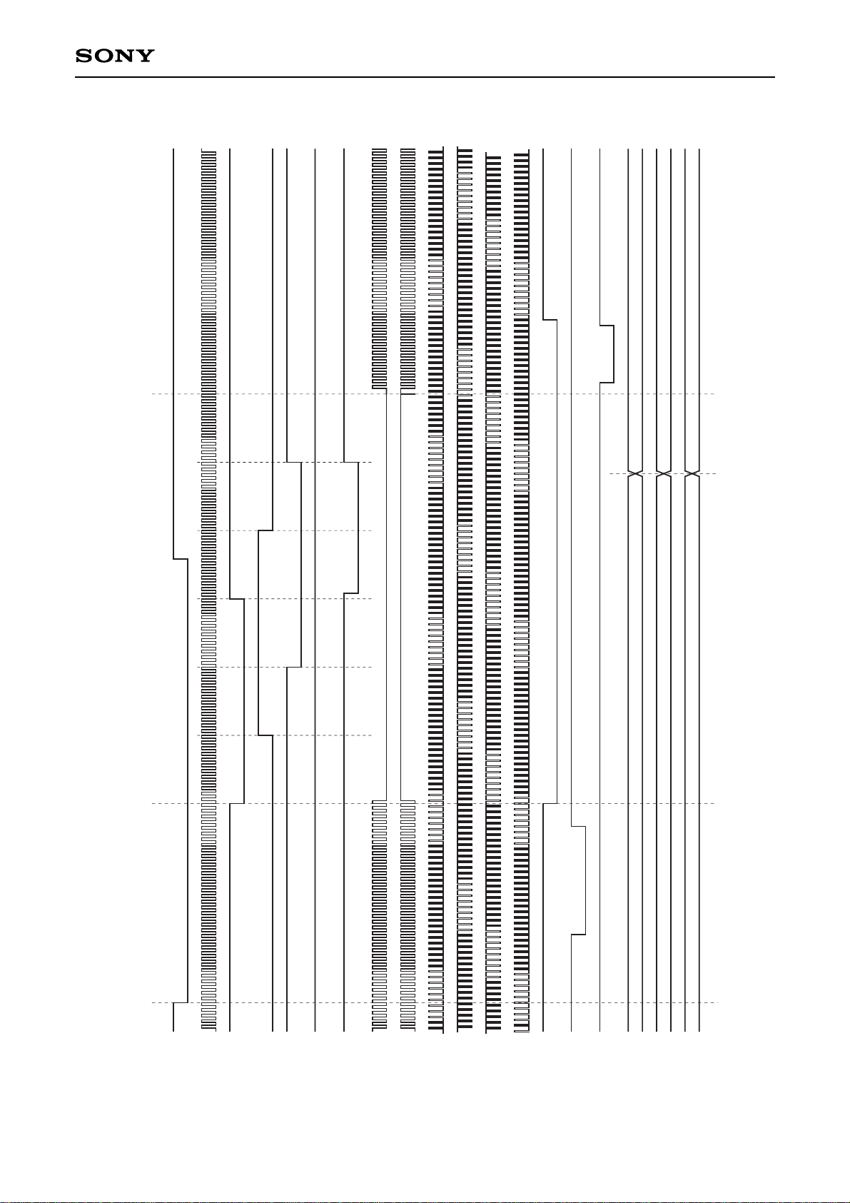
Normal Operation (horizontal synchronization)
780
1
1
35
35
78
107
47 59
71 83
95
72
95
35
12
31
120
109
93 119
HD
CL
XV1
XV2
XV3
XSG
(=High)
XSUB
H1
H2
RG
XSHP
XSHD
XRS
PBLK
XCPOB
XCPDM
ID
WEN
BUSY
XSUB may be kept high depending on the electronic shutter setting.
Page 17

—17—
CXD2434ATQ
780
1
1
35
35
78
107
47
59
71
83
520
551
576
12
31
93
109
119
HD
CL
XV1
XV2
XV3
XSG
XSUB
(=High)
H1
H2
RG
XSHP
XSHD
XRS
PBLK
(=Low)
XCPOB
XCPDM
ID
WEN
(=Low)
BUSY
=High(trig)
Low(others)
Normal Operation: readout timing (horizontal synchronization)
Page 18
—18—
CXD2434ATQ
1
27
1
14
508
1 2 3 4 5 6 7 8 1 2 3 4
TRIG
VD
HD
OUT
RG
XV1
XV2
XV3
XSG
XSUB
PBLK
XCPOB
XCPDM
ID
WEN
(WM=High)
WEN
(WM=Low)
BUSY
External Trigger Mode: high-speed electronic shutter, discharge (FSE=high, SMDE=high, SMD1=low, SMD2=high)
∗ See “3. Electronic Shutter” for the time from TRIG input to XSG.
∗ The fall of VD is invalid during the period while BUSY=high.
Page 19
—19—
CXD2434ATQ
External Trigger Mode: high-speed electronic shutter, when discharge starts (FSE=high, SMD1=low, SMD2=high)
1 2 3
780
1
35
35
42 49
56 63
77
70
72
95
12
35
31
93
TRIG
HD
CL
XV1
XV2
XV3
XSG
(=High)
XSUB
H1
H2
RG
XSHP
XSHD
XRS
PBLK
XCPOB
XCPDM
ID
WEN
BUSY
Page 20
—20—
CXD2434ATQ
499 500
HD
CL
XV1
XV2
XV3
XSG
(=High)
XSUB
H1
H2
RG
XSHP
XSHD
XRS
PBLK
=(Low)
XCPOB
(=High)
XCPDM
(=High)
ID
WEN
(=Low)
BUSY
(=High)
External Trigger Mode: high-speed electronic shutter, when discharge finishes (FSE=high, SMD1=low, SMD2=high)
Page 21
—21—
CXD2434ATQ
1
14
508
1 2 3 4 5 6 7 8 1 2 3 4
TRIG
VD
HD
OUT
RG
XV1
XV2
XV3
XSG
XSUB
PBLK
XCPOB
XCPDM
ID
WEN
(WM=High)
WEN
(WM=Low)
BUSY
External Trigger Mode: high-speed electronic shutter, no discharge (FSE=low, SMDE=high, SMD1=low, SMD2=X)
∗ See “3. Electronic Shutter” for the time from TRIG input to XSG.
∗ The fall of VD is invalid during the period while BUSY=high.
Page 22
—22—
CXD2434ATQ
1 2 3 4 5 6 7 8 1 2 3 4
1
27
1
14
508
TRIG
ESG
VD
HD
OUT
RG
XV1
XV2
XV3
XSG
XSUB
PBLK
XCPOB
XCPDM
ID
WEN
(WM=High)
WEN
(WM=Low)
BUSY
Example during ESG Input (FSE=high, SMDE=low, SMD1=low, SMD2=X)
The fall of VD is invalid during the period while BUSY=high.
Page 23
—23—
CXD2434ATQ
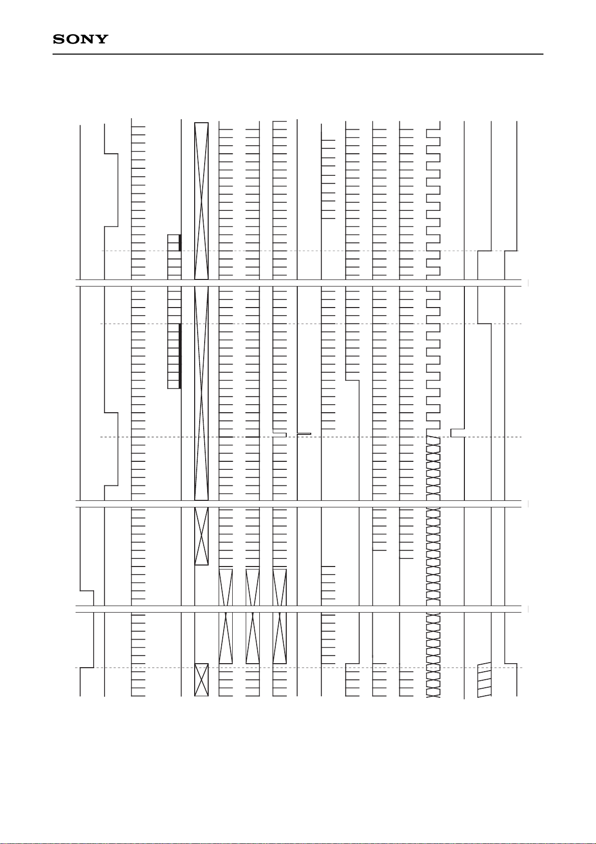
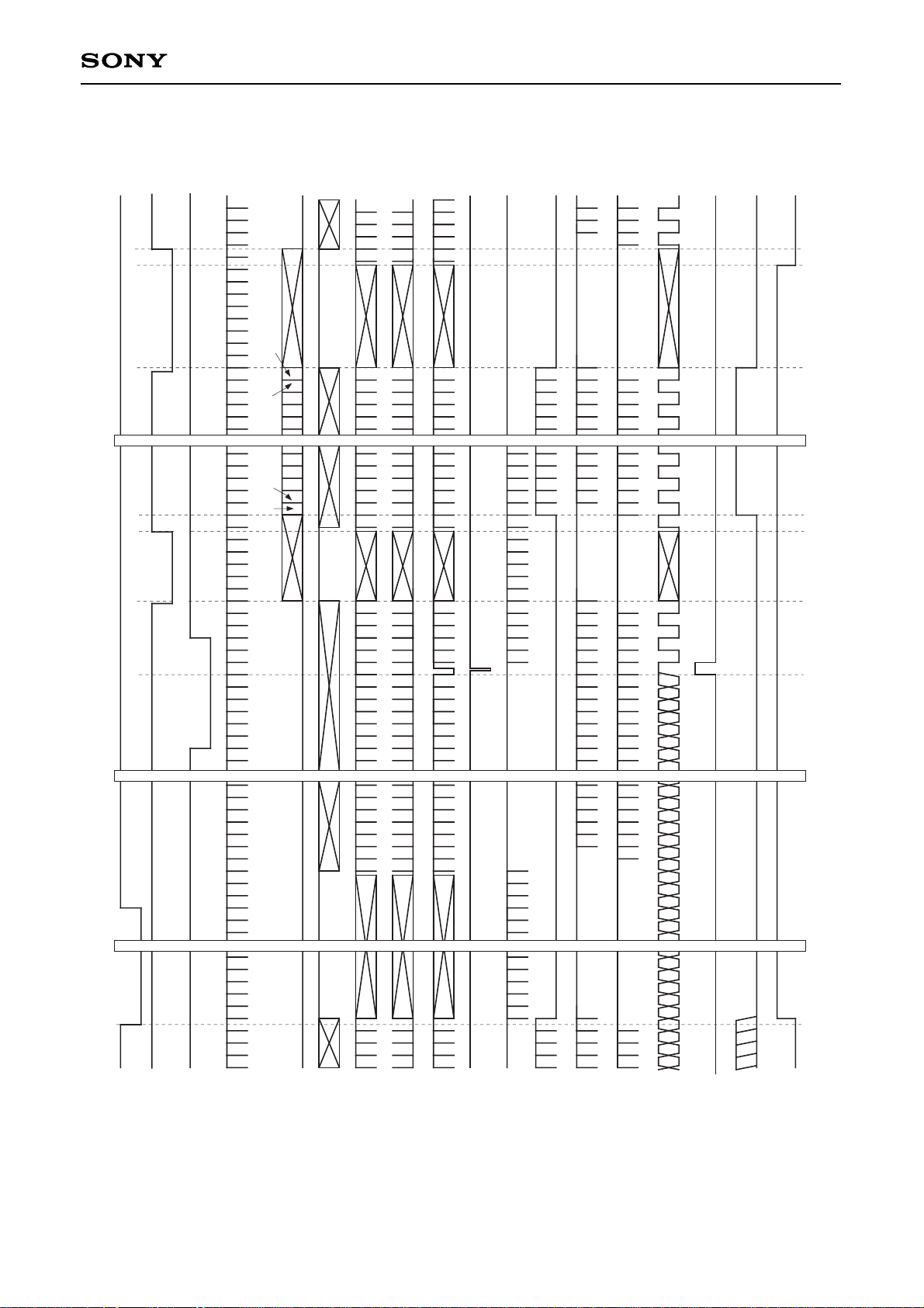
Example during EFS Input (trigger mode: FSE=high, SMDE=high, SMD1=low, SMD2=X)
1
27
1
6
13
98 99 339 340
256
264
TRIG
EFS
VD
HD
OUT
RG
XV1
XV2
XV3
XSG
XSUB
PBLK
XCPOB
XCPDM
ID
WEN
(WM=High)
WEN
(WM=Low)
BUSY
42 bits 104 times
×
The fall of VD is invalid during the period while BUSY=high.
Page 24

—24—
CXD2434ATQ
780
1
35
35
107
77
56 63
42 49
70
12
35
31
93
EFS
HD
CL
XV1
XV2
XV3
XSG
(=High)
XSUB
(=High)
H1
H2
RG
XSHP
XSHD
XRS
PBLK
XCPOB
XCPDM
ID
WEN
BUSY
During EFS Input, when discharge starts
Page 25

—25—
CXD2434ATQ
ID
EFS
HD
CL
XV1
XV2
XV3
XSG
(=High)
XSUB
H1
H2
RG
XSHP
XSHD
XRS
PBLK
=(Low)
XCPOB
(=High)
XCPDM
(=High)
WEN
(=Low)
BUSY
(=Low)
During EFS Input, when discharge finishes
Page 26
SONY CODE
EIAJ CODE
JEDEC CODE
PACKAGE MATERIAL
LEAD TREATMENT
LEAD MATERIAL
PACKAGE WEIGHT
EPOXY RESIN
SOLDER PLATING
42 ALLOY
PACKAGE STRUCTURE
48PIN TQFP (PLASTIC)
0.2g
TQFP-48P-L071
TQFP048-P-0707-AN
0.1
A
7.0 ± 0.2
36 25
9.0 ± 0.4
24
13
12
1
48
37
0.5 0.2 ± 0.1
M
0.08
DETAIL A
0.5 ± 0.2
1.0 ± 0.2
3° – 3°
+ 7°
0.1 ± 0.1
1.0 ± 0.1
1.27 MAX
0.125 ± 0.05
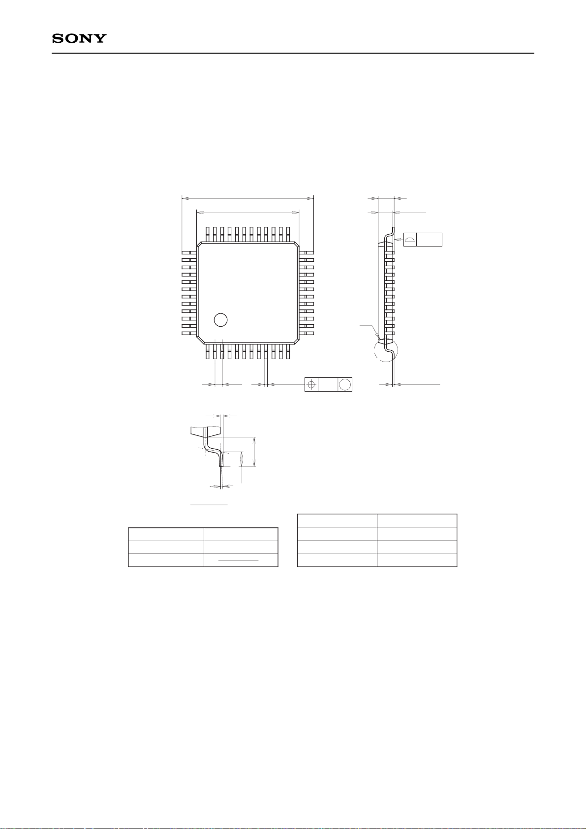
Package Outline Unit : mm
CXD2434ATQ
—26—
 Loading...