

Page 1
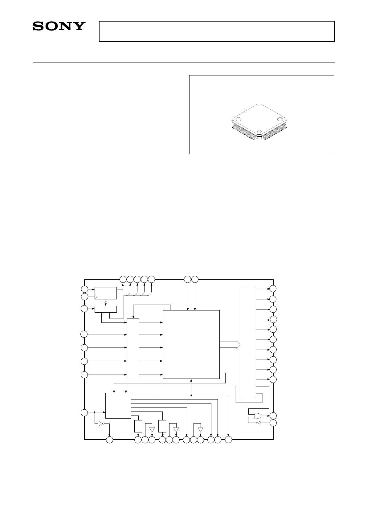
CCD Camera Timing Generator
Description
The CXD2422R generates the timing pulses
required for driving and signal processing CCDs with
480,000 pixels (EIA, effective pixels) and CCDs with
570,000 pixels (CCIR, effective pixels).
Features
• EIA and CCIR compatible
• Compatible with component digital and composite
digital recording format
• Compatible with field/frame accumulation modes
Applications
CCD cameras
Structure
Silicon gate CMOS IC
Applicable CCD Image Sensors
ICX062/063AL
Block Diagram
D0
D2
D1
2
3
Delay
1514
D3
4
V latch
16
Pulse Generation Circuit
Internal clock
Delay
19
18
SD
SC
LD
HTSG
FLD/FRM
EIA/CCIR
MODE
CLKI
30
31
32
Shutter data
58
61
62
63
33
51
Shift
Register
13
Latch
94
Reset
High-speed
Pulse
Generation
Circuit
34
SDO
1
Latch
XH gate
CXD2422R
64 pin LQFP (Plastic)
Absolute Maximum Ratings
• Supply voltage VDD VSS – 0.5 to +7.0 V
• Input voltage VI VSS – 0.5 to VDD + 0.5 V
• Output voltage VO VSS – 0.5 to VDD + 0.5 V
• Operating temperature
Topr –20 to +75 °C
• Storage temperature
Tstg –55 to +150 °C
Recommended Operating Conditions
• Supply voltage VDD 4.5 to 5.5 V
• Operating temperature
Topr –20 to +75 °C
VD
HD
6
5
39
XSG1
38
XSG2
44
XV1
XV2
43
XV3
42
41
35
26
22
21
28
27
XV4
XSUB
HCLP1
HCLP2
VCLP
PBLK
PBLKON
Output
F.F.
7
37
53
54
20
36
52
CLKO
SHP
BAI
BAO
SHD
BBI
BBO
XRG
BCI
BCO
XH1
XH2
CLK
Sony reserves the right to change products and specifications without prior notice. This information does not convey any license by
any implication or otherwise under any patents or other right. Application circuits shown, if any, are typical examples illustrating the
operation of the devices. Sony cannot assume responsibility for any problems arising out of the use of these circuits.
– 1 –
E94Y30-ST
Page 2

Pin Configuration
CXD2422R
NC
NC
SDO
BCO
BCI
XRG
VSS
VDD
NC
HTSG
RST
TEST12
49
50
51
52
53
54
55
56
58
59
57
60
TEST11
48
TEST10
47
TEST9
46
TEST8
45
44
XV1
43
XV2
XV3
SS
XV4
V
XSG1
XSG2
40
4142
39
38
37
XH1
36
XH2
35
XSUB
CLKO
34
33
CLKI
32
31
30
29
28
27
26
25
24
23
22
21
LD
SC
SD
TEST7
PBLK
PBLKON
HCLP1
TEST6
VDD
SS
V
HCLP2
VCLP
FLD/FRM
EIA/CCIR
MODE
TEST13
61
62
63
64
BBO
20
BBI
19
SHD
18
NC
17
6
1
2
3
D0
D1
D2
5
4
D3
VD
HD
7
CLK
9
8
SS
V
10
TEST1
11
TEST2
TEST3
12
TEST4
13
TEST5
14 15
SHP
BAI
16
BAO
– 2 –
Page 3
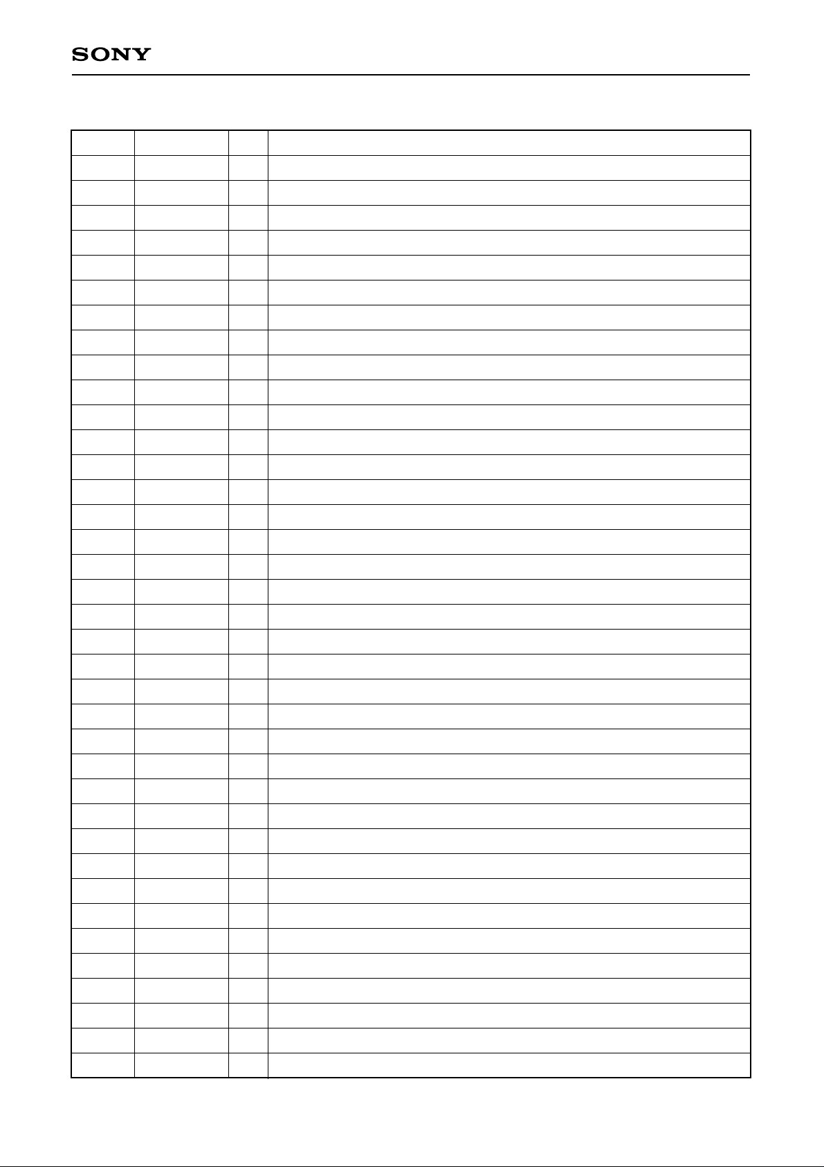
Pin Description
Pin No. Symbol I/O Description
CXD2422R
1
2
3
4
5
6
7
8
9
10
11
12
13
14
15
16
17
D0
D1
D2
D3
VD
HD
CLK
VSS
TEST1
TEST2
TEST3
TEST4
TEST5
SHP
BAI
BAO
(NC)
Extended I/O output.
O
Extended I/O output.
O
Extended I/O output.
O
Extended I/O output.
O
Vertical sync signal input. (With pull-up resistor)
I
Horizontal sync signal input. (With pull-up resistor)
I
Two frequency divider output of Pin 33.
O
—
Test input (normally Low). (With pull-down resistor)
I
Test input (normally Low). (With pull-down resistor)
I
Test input (normally Low). (With pull-down resistor)
I
Test input (normally Low). (With pull-down resistor)
I
Test input (normally Low). (With pull-down resistor)
I
CCD output precharge level sampling pulse output.
O
Buffer input (for phase adjustment of SHP). (With pull-up resistor)
I
Non-inversed output of BAI.
O
—
18
19
20
21
22
23
24
25
26
27
28
29
30
31
32
33
34
SHD
BBI
BBO
VCLP
HCLP2
VSS
VDD
TEST6
HCLP1
PBLKON
PBLK
TEST7
SD
SC
LD
CLKI
CLKO
CCD output signal level sampling pulse output.
O
Buffer input (for phase adjustment of SHD). (With pull-up resistor)
I
Non-inversed output of BBI.
O
Vertical clamp pulse output.
O
Horizontal (dummy bit block) clamp pulse output.
O
—
—
Test input (normally High). (With pull-up resistor)
I
Horizontal (OPB block) clamp pulse output.
O
Output ON/OFF of PBLK. (High: ON) (With pull-up resistor).
I
Preblanking pulse output.
O
Test input (normally High). (With pull-up resistor)
I
Serial data input for electronic shutter control. (With pull-up resistor)
I
Clock input for electronic shutter control. (With pull-up resistor)
I
Latch pulse input for electronic shutter control. (With pull-up resistor)
I
Clock input.
I
Inversed output of CLKI.
O
35
36
37
XSUB
XH2
XH1
Substrate pulse output for electronic shutter.
O
Clock output for horizontal register drive.
O
Clock output for horizontal register drive.
O
– 3 –
Page 4

Pin No. Symbol I/O Description
CXD2422R
38
39
40
41
42
43
44
45
46
47
48
49
50
51
52
53
54
XSG2
XSG1
VSS
XV4
XV3
XV2
XV1
TEST8
TEST9
TEST10
TEST11
(NC)
(NC)
SDO
BCO
BCI
XRG
Sensor charge readout pulse output.
O
Sensor charge readout pulse output.
O
—
Clock output for vertical register drive.
O
Clock output for vertical register drive.
O
Clock output for vertical register drive.
O
Clock output for vertical register drive.
O
Test output (normally open).
O
Test output (normally open).
O
Test output (normally open).
O
Test output (normally open).
O
—
—
Serial data output for electronic shutter control.
O
Non-inversed output of BCI.
O
Buffer input (for phase adjustment of XRG). (With pull-up resistor)
I
Reset gate pulse output of output block.
O
55
56
57
58
59
60
61
62
63
64
VSS
VDD
(NC)
HTSG
RST
TEST12
FLD/FRM
EIA/CCIR
MODE
TEST13
—
—
—
Readout pulse (XSG1, 2) ON/OFF. (High: OFF) (With pull-down resistor)
I
Test input (normally High). (With pull-up resistor)
I
Test input (normally Low). (With pull-up resistor)
I
High: Field accumulation mode, Low: Frame accumulation mode.
I
(With pull-up resistor)
High: EIA, Low: CCIR. (With pull-up resistor)
I
High: Component digital mode, Low: Composite digital mode.
I
(With pull-up resistor)
Test input (normally Low). (With pull-up resistor)
I
Note) TEST12 and TEST13 have a built-in pull-up resistor.
Be sure to fix them at Low.
– 4 –
Page 5
CXD2422R
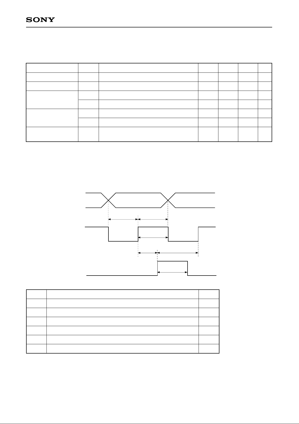
Electrical Characteristics
1) DC characteristics (VDD = 4.5 to 5.5V, Topr = –20 to +75°C)
Item
Supply voltage
Input/Output voltages
Symbol
VDD
VI, VO
Conditions Min. Typ. Max. Unit
VIH
Input voltage
VIL
VOH
IOH = –2mA
Output voltage
Pull-up/
Pull-down resistors
VOL
RPU,
RPD
IOL = 4mA
VIL = 0V, VIH = VDD
2) AC characteristics
2)-1. Pulses for electronic shutter control (SD, SC, LD)
SD
4.5
VSS
0.7VDD
VDD – 0.8
40k
5.0
100k
5.5
VDD
0.3VDD
0.4
250k
V
V
V
V
V
V
Ω
Symbol
ts1
tH1
tw1
ts2
tH2
tw2
ts1 t
SC
LD
H1
tw1
ts2 t
Item Min.
SD set-up time, activated by the rising edge of SC
SD hold time, activated by the rising edge of SC
SC pulse width
SC set-up time, activated by the rising edge of LD
SC hold time, activated by the rising edge of LD
LD pulse width
H2
tw2
20ns
20ns
20ns
20ns
20ns
20ns
– 5 –
Page 6
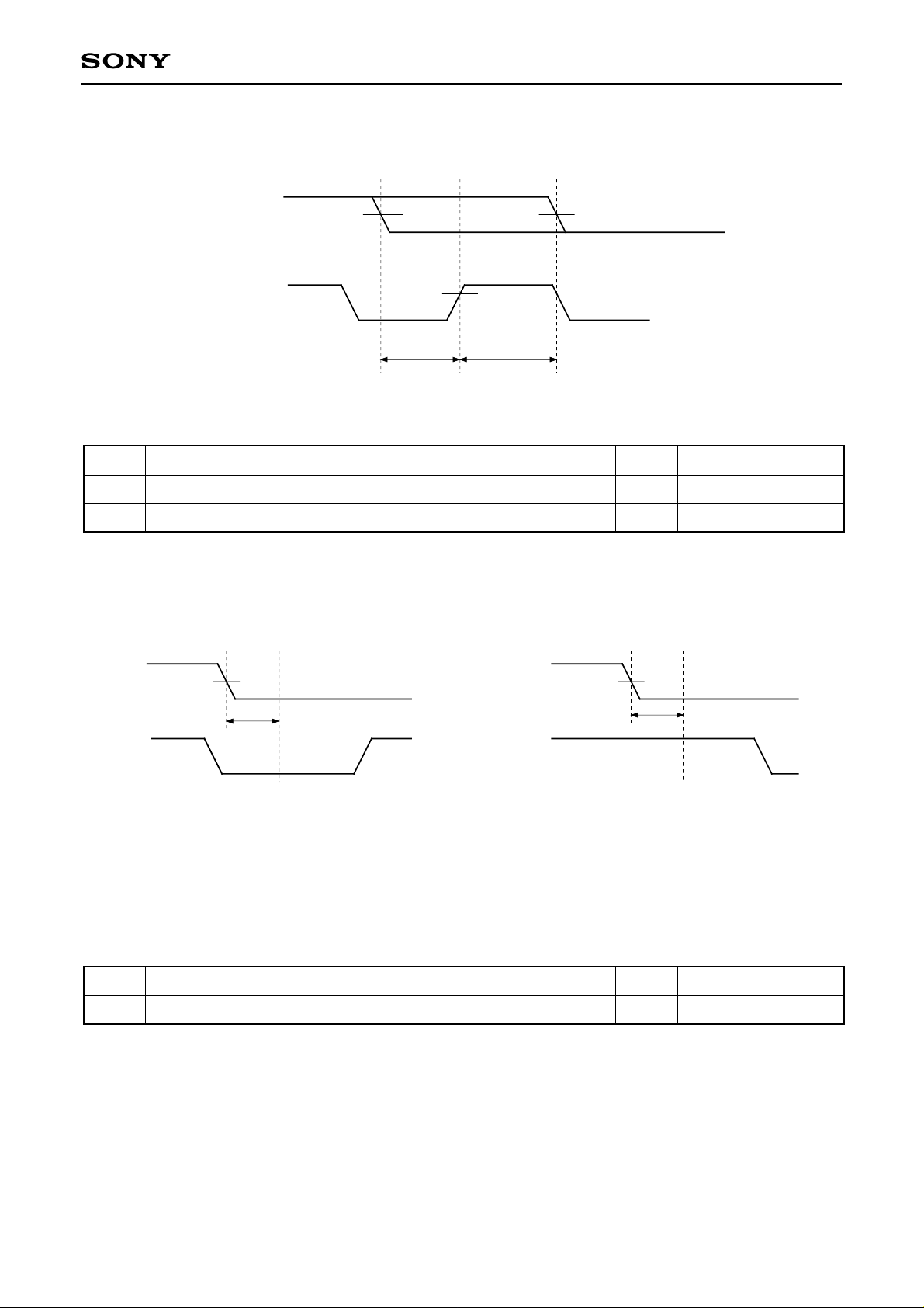
2)-2. HD/VD take-in characteristics
CXD2422R
HD, VD
CLK
1.6V 1.6V
Symbol
ts3
th3
HD/VD set-up time, activated by CLK
HD/VD hold time, activated by CLK
2)-3. Field discrimination characteristics
DD
0.7V
ts3 th3
(VDD = 4.5 to 5.5V, Topr = –20 to +75°C)
Definition Min. Typ. Max. Unit
4
0
ns
ns
VD
HD
1.6V
tpd1
When the HD logic level is Low tpd1 after
VD falls, the field is discriminated as an
ODD (EVEN with CCIR) field.
Symbol
tpd1
Field discriminating clock phase, activated by the falling edge of VD 890 ns
VD
HD
1.6V
tpd1
When the HD logic level is High tpd1 after
VD falls, the field is discriminated as an
EVEN (ODD with CCIR) field.
(VDD = 4.5 to 5.5V, Topr = –20 to +75°C)
Definition Min. Typ. Max. Unit
– 6 –
Page 7
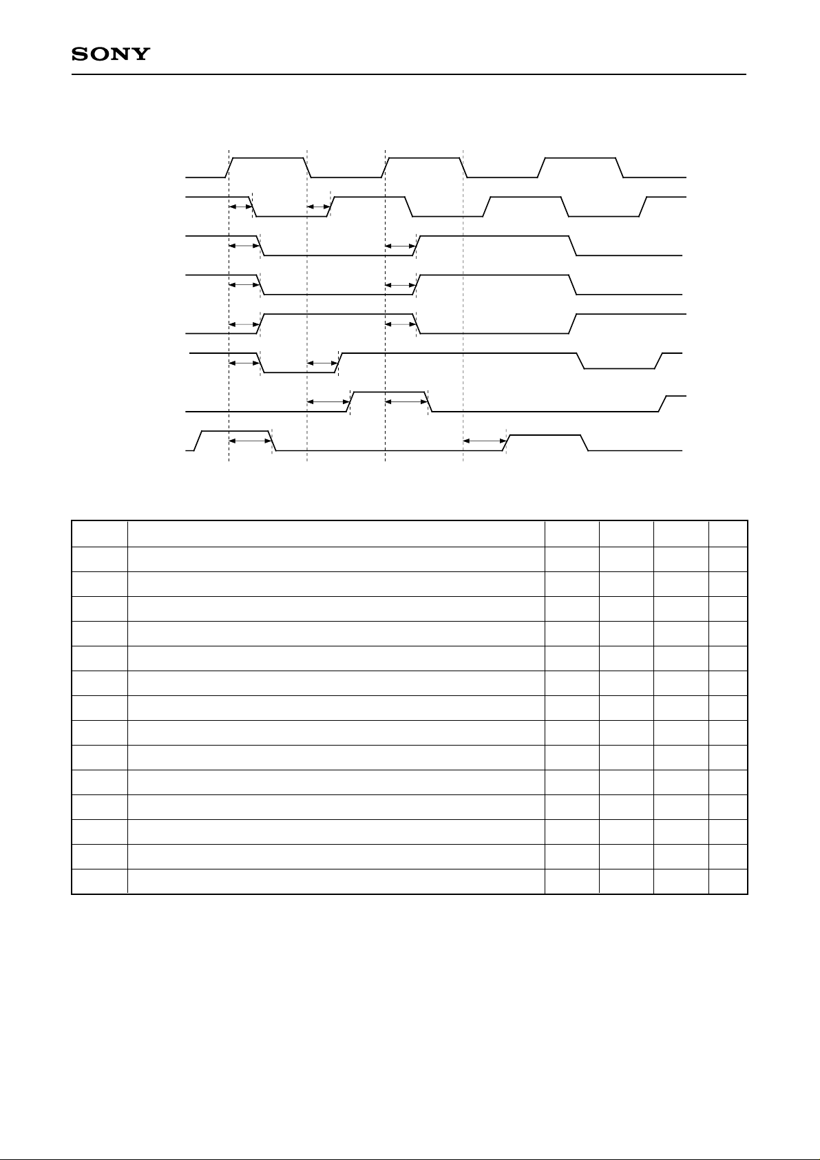
2)-4. CLKO, CLK, XH1, XH2, XRG, SHP, SHD phase characteristics
CLKI
CXD2422R
CLKO
CLK
XH1
XH2
XRG
SHP
SHD
tpd2
tpd4
tpd6
tpd8
tpd10
tpd14
tpd3
tpd5
tpd7
tpd9
tpd11
tpd12
tpd13
tpd15
(VDD = 4.5 to 5.5V, Topr = –20 to +75°C, load capacitance = 10pF)
Symbol Definition Min. Typ. Max. Unit
tpd2
tpd3
CLKO falling delay time against CLKI
CLKO rising delay time against CLKI
3.5
4.0
6.2
7.2
12.1
14.1
ns
ns
tpd4
tpd5
tpd6
tpd7
tpd8
tpd9
tpd10
tpd11
tpd12
tpd13
tpd14
tpd15
CLK2 falling delay time against CLKI
CLK2 rising delay time against CLKI
XH1 falling delay time against CLKI
XH1 rising delay time against CLKI
XH2 rising delay time against CLKI
XH2 falling delay time against CLKI
XRG falling delay time against CLKI
XRG rising delay time against CLKI
SHP rising delay time against CLKI
SHP falling delay time against CLKI
SHD falling delay time against CLKI
SHD rising delay time against CLKI
5.2
6.5
5.2
6.4
5.7
5.3
4.7
5.2
8.1
7.9
7.9
8.6
9.3
11.6
8.8
11.4
10.2
9.4
8.4
9.2
14.4
14.1
14.1
15.2
18.3
22.8
17.2
22.4
20.3
18.5
16.5
18.1
28.3
27.6
27.6
29.8
ns
ns
ns
ns
ns
ns
ns
ns
ns
ns
ns
ns
– 7 –
Page 8
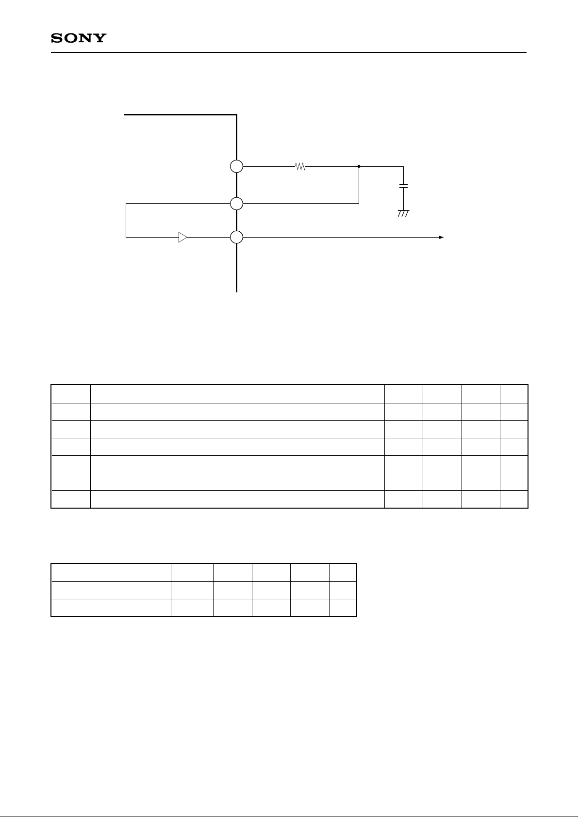
Phases of SHP, SHD, and XRG pulses can be adjusted using on-chip buffers.
Internal CXD2422R
CXD2422R
SHP
15
BAI
16
BAO
17
R
C
SHP
Delay times of SHP, SHD, and XRG can be adjusted with C and R.
Delay characteristics of on-chip buffers (VDD = 4.5 to 5.5V, Topr = –20 to +75°C, load capacitance = 10pF)
Symbol Definition Min. Typ. Max. Unit
tpd16
tpd17
Rising delay time from BAI to BAO
Falling delay time from BAI to BAO
4.0
2.8
7.1
5.5
13.9
10.7
ns
ns
tpd18
tpd19
tpd20
tpd21
Rising delay time from BBI to BBO
Falling delay time from BBI to BBO
Rising delay time from BCI to BCO
Falling delay time from BCI to BCO
3) I/O pin capacitances (VDD = VI = 0V, f = 1MHz)
Item Symbol Min. Typ. Max. Unit
Input pin capacitance
Output pin capacitance
CIN
COUT
9
11
pF
pF
4.0
3.0
4.3
3.4
7.0
5.4
7.6
6.0
13.8
10.7
15.0
11.7
ns
ns
ns
ns
– 8 –
Page 9
Description of Operation
1) Mode setting
Symbol Pin No. Low High
CXD2422R
EIA/CCIR
MODE
FLD/FRM
HTSG
PBLKON
62
63
61
58
27
CCIR
Composite digital mode
Clock (CLKI) input
EIA 35.79545MHz
(2275fH = 10fsc)
CCIR 35.46895MHz
(2270+8/625fH = 8fsc)
Frame accumulation
XSG1 and XSG2 pulses are output.
PBLK is fixed at High.
EIA
Component digital mode
Clock (CLKI) input
EIA 36MHz
(2288fH)
CCIR 36MHz
(2304fH)
Field accumulation
XSG1 and XSG2 pulses are fixed at
High. (Readout suspended)
PBLK pulse is output.
– 9 –
Page 10
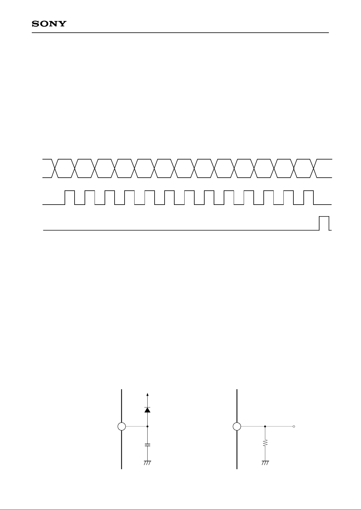
2) Inputting serial data
The accumulation time of the electronic shutter is controlled by external serial data.
Input pins (SD, SC, and LD) are used to input serial data.
SD: Serial data input
SC: Clock input
LD: Latch pulse input
The following is the serial data timing chart.
CXD2422R
SD
SC
LD
D3 D2 D1 D0 S8 S7 S6 S5 S4
S3 S2 S1 S0
D3 to D0: Not related to the accumulation time of the electronic shutter. Data are output to D3 to D0 pins
after converted into parallel data and being latched at LD.
S8 to S0: Sdata is set in 9-bit binary with S8 as MSB (High: 1, Low: 0). ON/OFF of the electronic shutter
and the accumulation time are determined by Sdata.
The calculation on the next page is for the accumulation time in each mode.
The data for SD are input to the internal 13-bit shift register, and the data can be retrieved as serial data at
SDO pin.
Note) The electronic shutter might operate from turning power on to inputting serial data. To prevent this
operation, process RST and LD pins as shown in the following figures. Be careful, however, as serial
data cannot be received before the voltage at RST rises.
DD
V
(with pull-up resistor)
RST
59
(with pull-up resistor)
1000p
LD
32
4.7k
– 10 –
Page 11
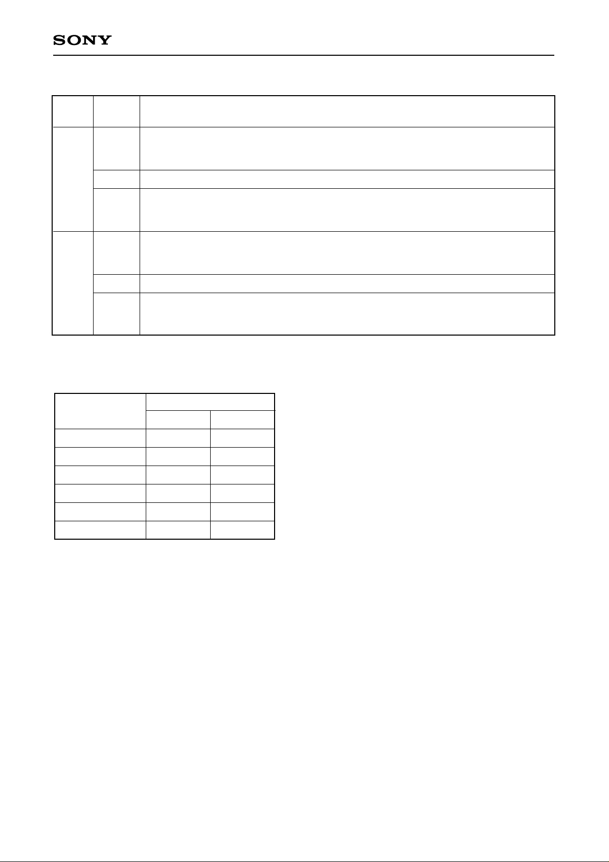
Accumulation time of electronic shutter
CXD2422R
EIA/
CCIR
EIA
Sdata
0
to
261
262
{(261 – Sdata)/15734} + 1/25678 (Component digital mode)
{(261 – Sdata)/15734} + 1/25532 (Composite digital mode)
Input prohibited
Accumulation time (s)
263
to
Electronic shutter OFF
511
CCIR
0
to
311
312
{(311 – Sdata)/15625} + 1/25678 (Component digital mode)
{(311 – Sdata)/15625} + 1/25299 (Composite digital mode)
Input prohibited
313
to
Electronic shutter OFF
511
The Sdata values corresponding to representative shutter speeds are listed below.
Shutter speed
1/100
1/125
1/250
1/500
1/1000
1/2000
EIA
104 (068h)
136 (088h)
199 (0C7h)
230 (0E6h)
246 (0F6h)
254 (0FEh)
Sdata
CCIR
155 (09Bh)
187 (0BBh)
249 (0F9h)
280 (118h)
296 (128h)
304 (130h)
– 11 –
Page 12
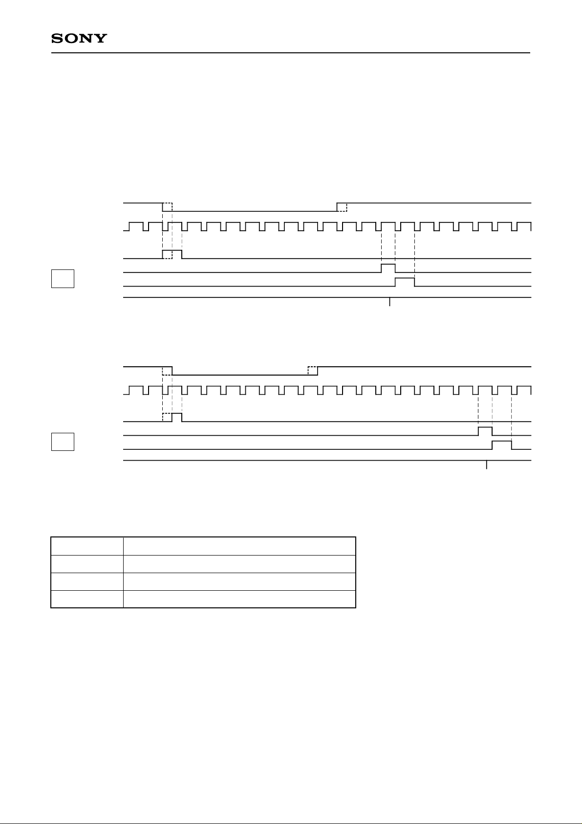
3) Latch pulse timing
Various mode switchings and shutter data are taken in by field. The latch pulse timing is as follows
(The broken lines show timing in the EVEN FIELD.):
EIA
VD
HD
VLT1
VLT2
IT
VLT3
XSG1,2
CXD2422R
CCIR
VD
HD
VLT1
VLT2
IT
VLT3
XSG1,2
Latch pulse
VLT1
VLT2
VLT3
Latched data
EIA/CCIR, MODE, HTSG
Shutter data (S8 to S0)
FLD/FRM
– 12 –
Page 13
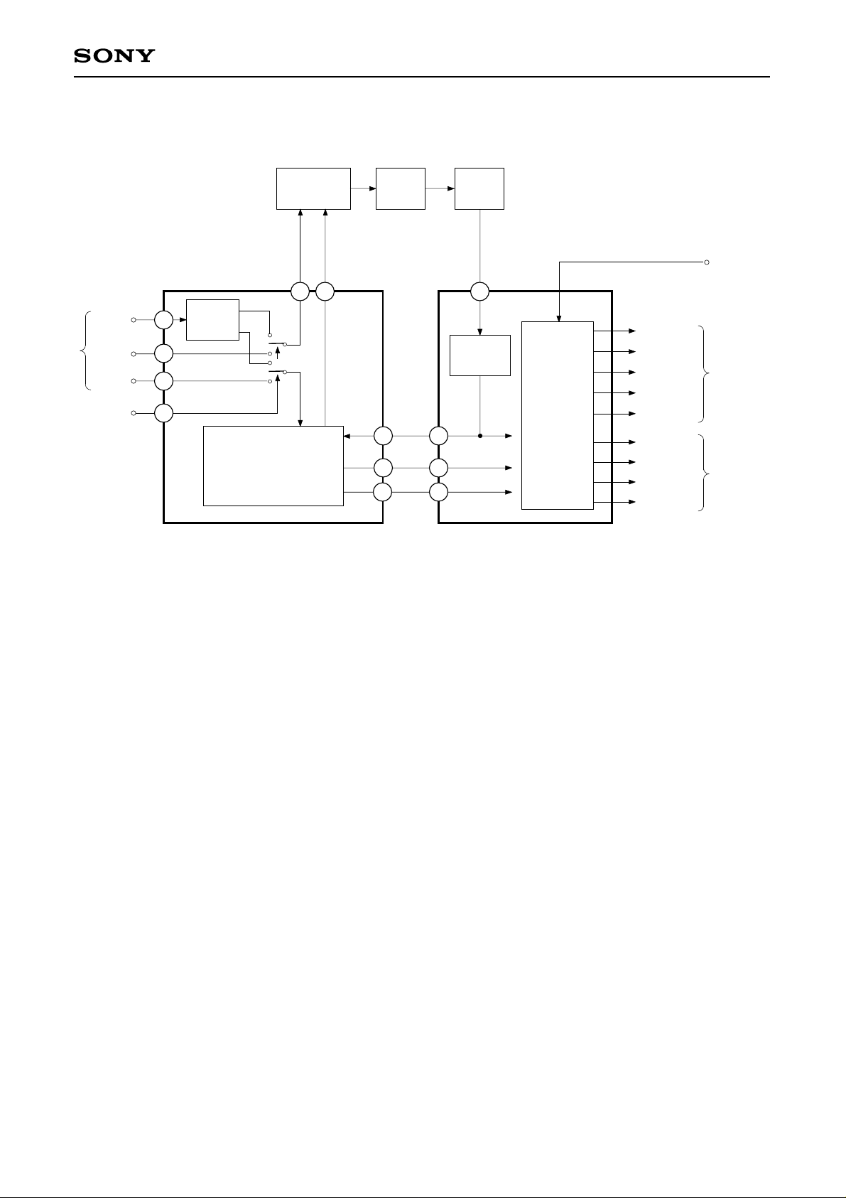
Example of System Configuration
CXD2422R
External sync
signal
SYNC
HD
VD
MODE1
15
14
13
26
Separation
fH and fV
fH
of
fV
Frequency Division/
Pulse Generation Circuit
CXD8302Q CXD2422R (TG)
Phase
Comparator
19
20
INTf
LPF VCO
HEXTfH
CLK
38
HD
41
VD
42
Frequency
7
6
5
33
1/2
Division
36MHz (Component digital)
35.79545MHz (Composite digital, EIA)
35.56895MHz (Composite digital, CCIR)
Electronic shutter serial data
XH1, 2
XRG
XSUB
Pulse
Generation
Circuit
XV1 to 4
XSG1, 2
SHP, SHD
HCLP1, 2
VCLP
PBLK
To each
driver
To signal
processing
circuit
Note) 1. Either SYNC or VD/HD is used as external sync signal. When SYNC is used (SYNC synchronous
mode), fix MODE1 to High; when VD/HD is used (VD/HD Synchronous mode), fix MODE1 to Low.
2. Be sure to do phase comparison of the falling edge of EXTfH and INTfH for SYNC synchronous
mode.
– 13 –
Page 14
285
280
CXD2422R
∗2
8
7
6
5
3
4
2
1
275
∗1
270
493
265
494
260
∗2
9
20
15
8
7
6
5
4
3
2
1
∗1
10
5
(525) 0
520
VD
BLK
HD
XV1
XV2
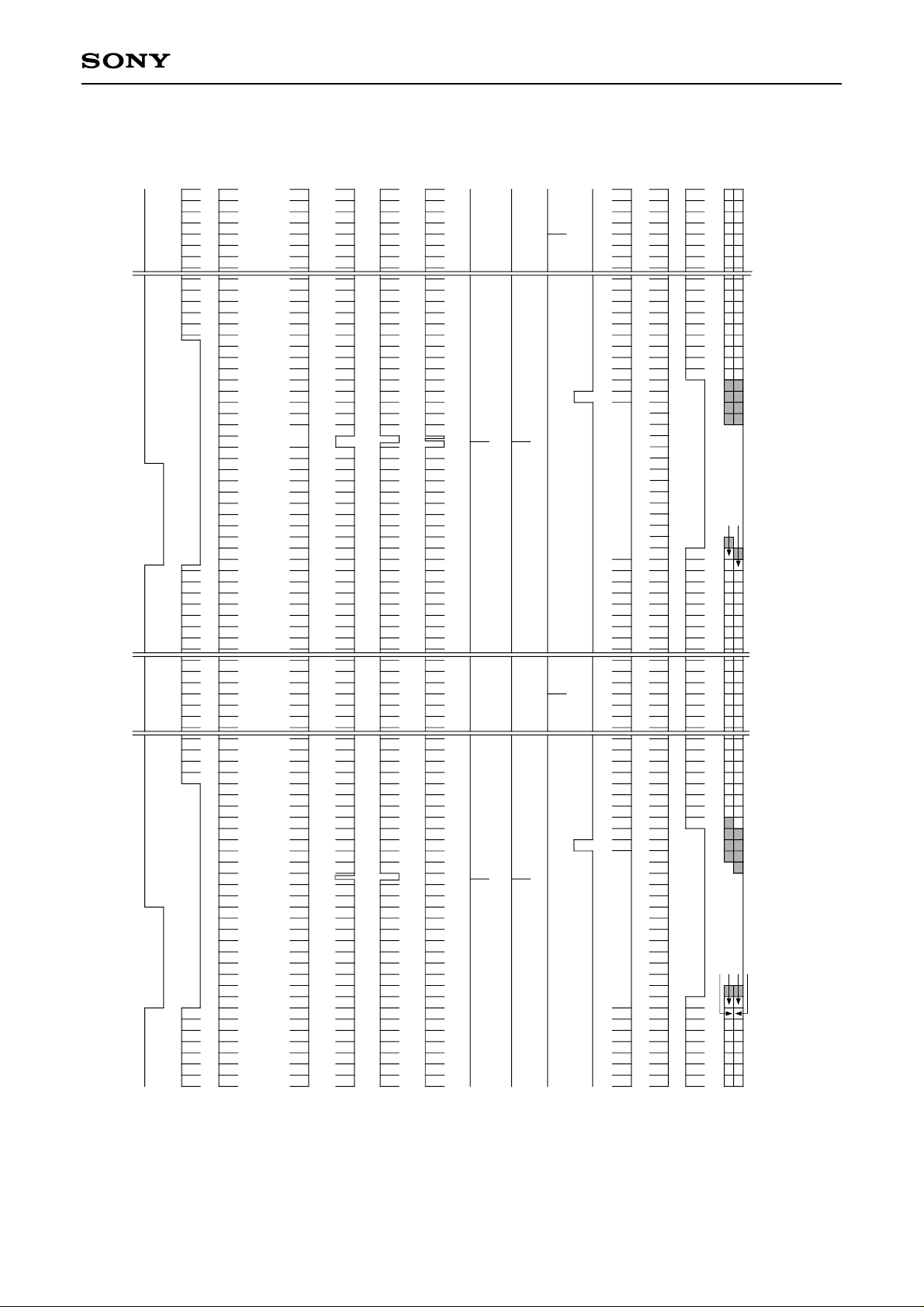
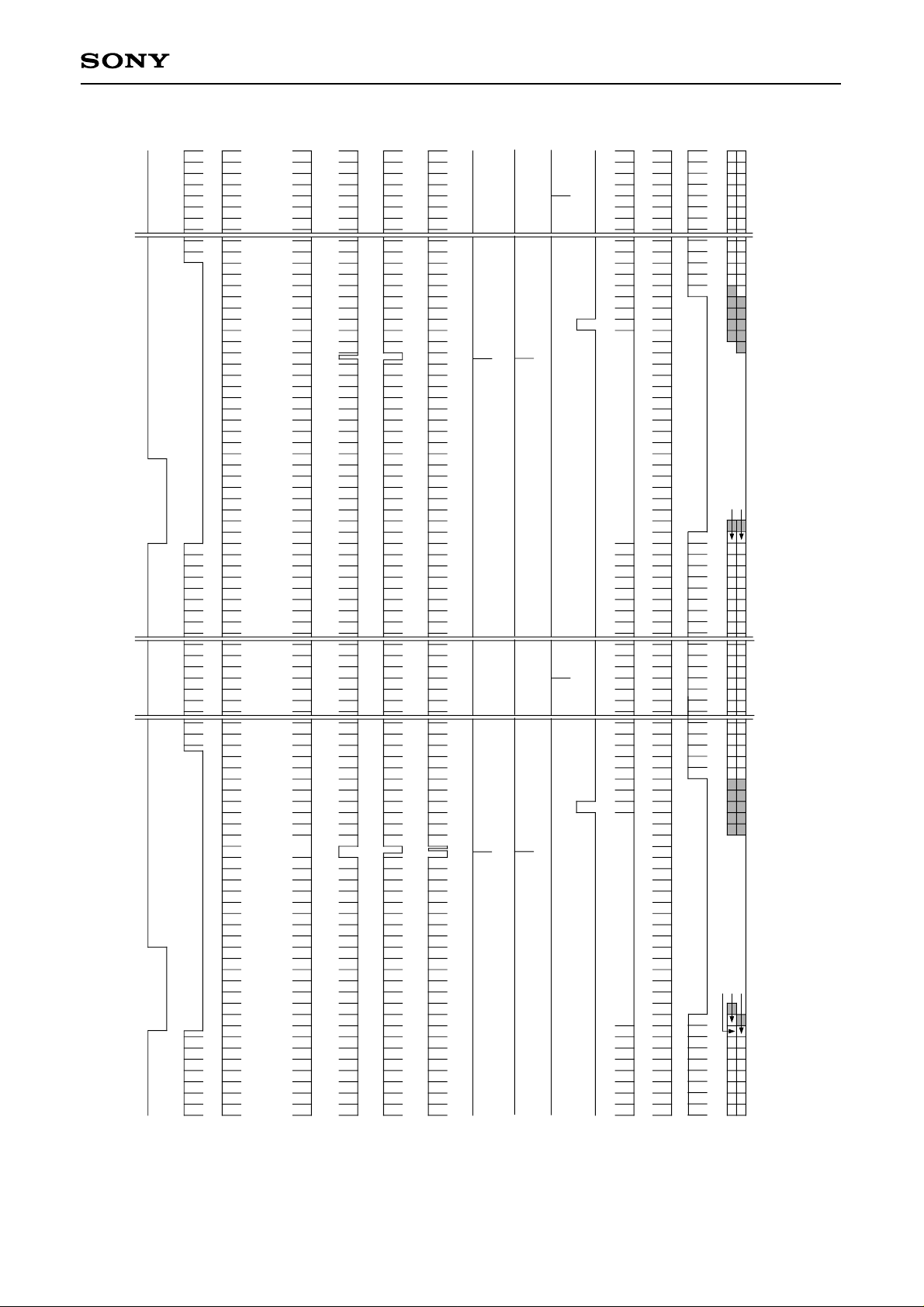
Timing Chart (1) EIA vertical direction
XV3
XV4
– 14 –
XSG1
XSG2
XSUB
VCLP
HCLP1
HCLP2
PBLK
491
494
493
CCD
OUT
492
These pulses are not output during frame accumulation.
These pulses are output at the position determined by shutter data.
∗1
∗2
Page 15
335
CXD2422R
∗2
68
79
5
4
2
3
1
330
∗1
325
320
581
582
315
310
∗2
57
25
3
1
68
4
2
20
15
10
5
1
(625) 0
620
VD
BLK
HD
XV1
XV2
Timing Chart (2) CCIR vertical direction
XV3
XV4
– 15 –
∗1
XSG1
XSG2
XSUB
VCLP
HCLP1
HCLP2
PBLK
580
582
CCD
581
OUT
These pulses are not output during frame accumulation.
These pulses are output at the position determined by shutter data.
∗1
∗2
Page 16
fH = 1144
170
160
150
164
CXD2422R
164
160
128
140
130
120
110
100
90
80
70
60
50
60
75
70
85
80
55
90
65
130
95
47
138
53
136
55
40
30
20
2
VCLP
15
HCLP1
HCLP2
0
HD
0
BLK
10
0 (1144)
CLK
XV1
XV2
XV3
XV4
XSUB
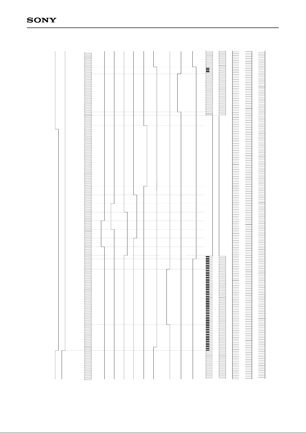
Timing Chart (3) EIA horizontal direction, Component digital mode
– 16 –
PBLK
XH1
XH2
XRG
SHP
SHD
Page 17
170.5
CXD2422R
fH = 1137.5
128
160.5
150.5
140.5
130
120
110
100
90
80
85
80
90
130
95
157.5
157.5
153.5
131
129
60
75
70
55
65
47
15
2
53
55
70
60
50
40
30
20
10
0
0
0 (1137.5)
HD
BLK
CLK
XV1
XV2
XV3
XV4
XSUB
VCLP
HCLP1
HCLP2
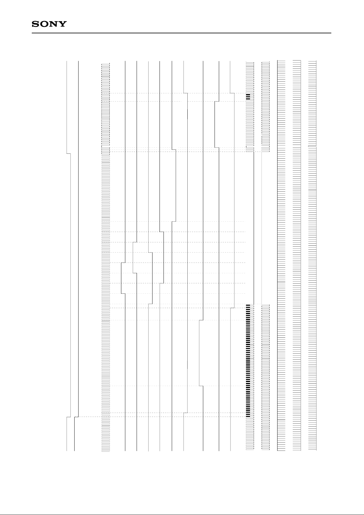
Timing Chart (4) EIA horizontal direction, Composite digital mode
– 17 –
PBLK
XH1
XH2
XRG
SHP
SHD
Page 18
CXD2422R
fH = 1152
128
170
160
150
140
130
120
110
100
90
80
70
75
70
85
80
90
130
95
172
172
168
146
144
55
XV3
65
XV4
XSUB
2
VCLP
47
15
HCLP1
HCLP2
HD
60
60
50
40
30
20
10
0
0
BLK
0 (1152)
CLK
XV1
XV2
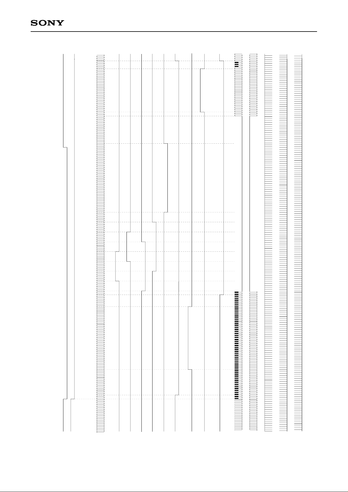
Timing Chart (5) CCIR horizontal direction, Component digital mode
53
PBLK
XH1
55
XH2
XRG
SHP
SHD
– 18 –
Page 19
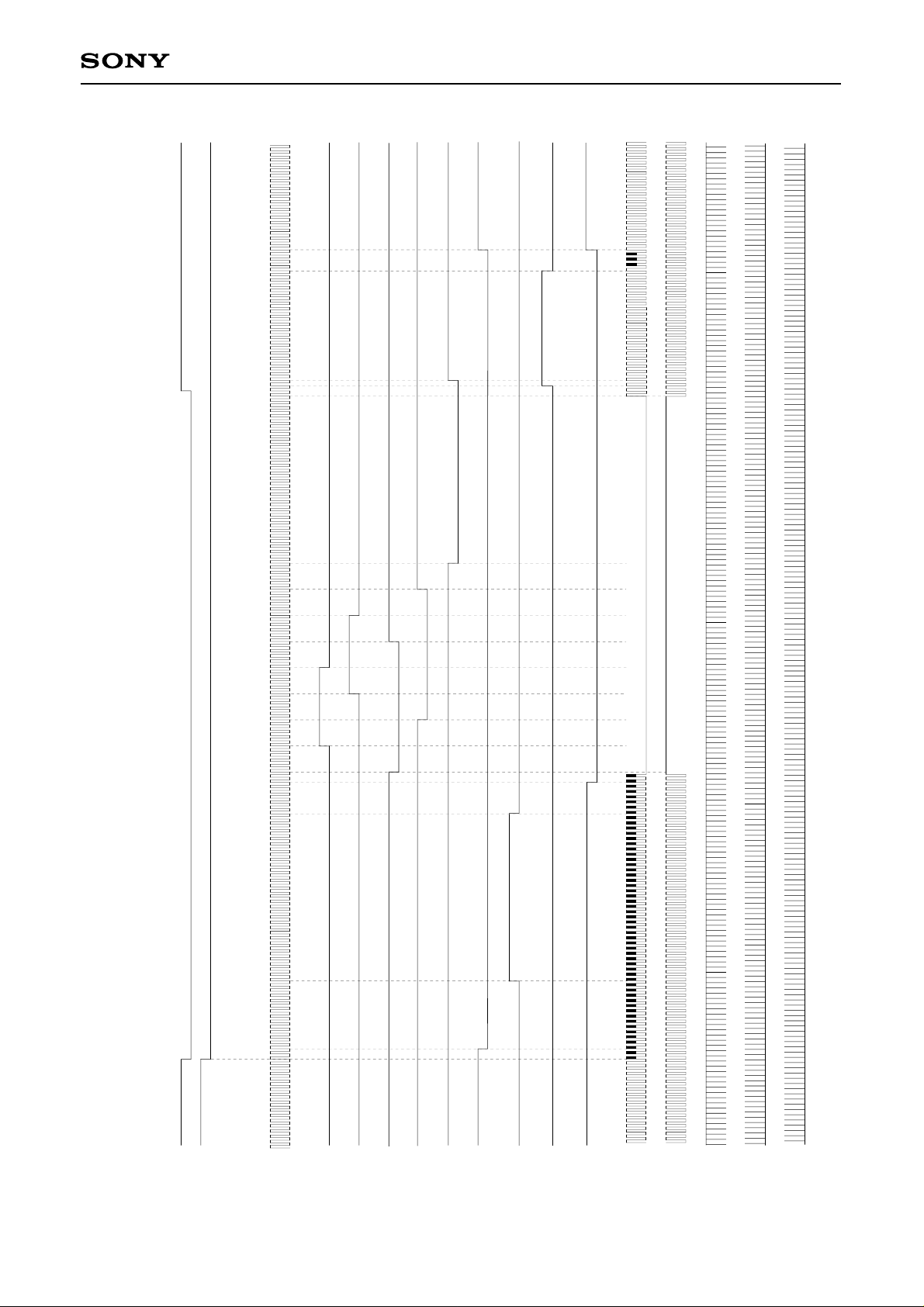
fH = 1135
170
160
150
140
155
CXD2422R
155
151
128
130
120
110
100
90
80
70
60
50
60
75
70
85
80
55
90
65
130
95
47
129
53
127
55
40
30
20
2
VCLP
15
HCLP1
HCLP2
HD
10
0
0
BLK
0 (1135)
CLK
XV1
XV2
XV3
XV4
XSUB
Timing Chart (6) CCIR horizontal direction, Composite digital mode
– 19 –
PBLK
XH1
XH2
XRG
SHP
SHD
Page 20
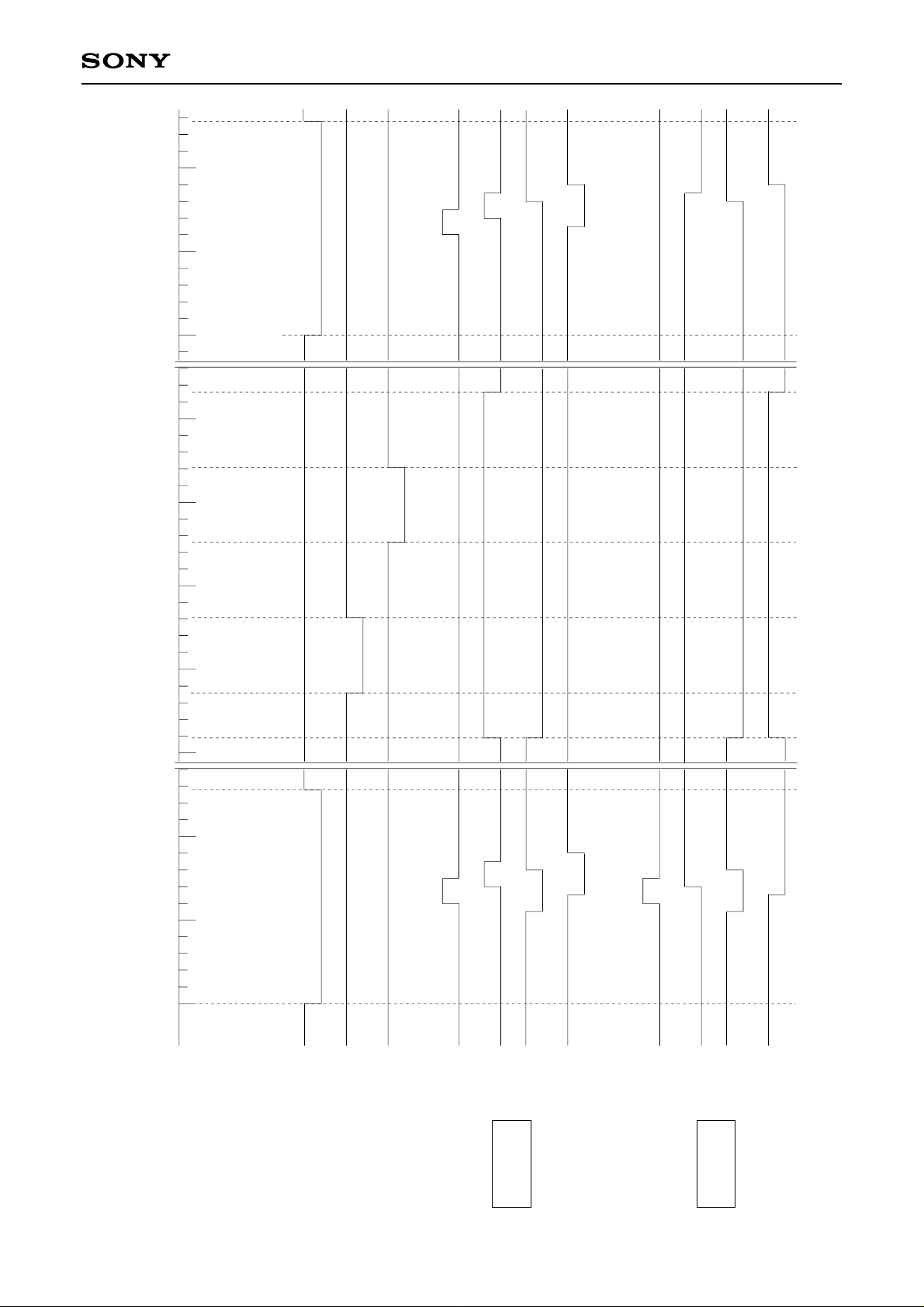
128
CXD2422R
0 50 100
= 1144 (EIA, Component digital)
1137.5 (EIA, Composite digital)
1152 (CCIR, Component digital)
1135 (CCIR, Composite digital)
900 950
850
921
876
75
60
85
70
966
80
90
65
85
90
80
966
0 50 100 750 800
CLK
128
HD
831
786
XSG1
XSG2
75
60
XV1
759
70 85
XV2
80
55
759
XV3
65 90
XV4
75
60
XV1
70
XV2
80
55
759
XV3
759
65
XV4
Timing Chart (7) Readout interval
– 20 –
EIA: ODD
CCIR: EVEN
EIA: EVEN
CCIR: ODD
Page 21
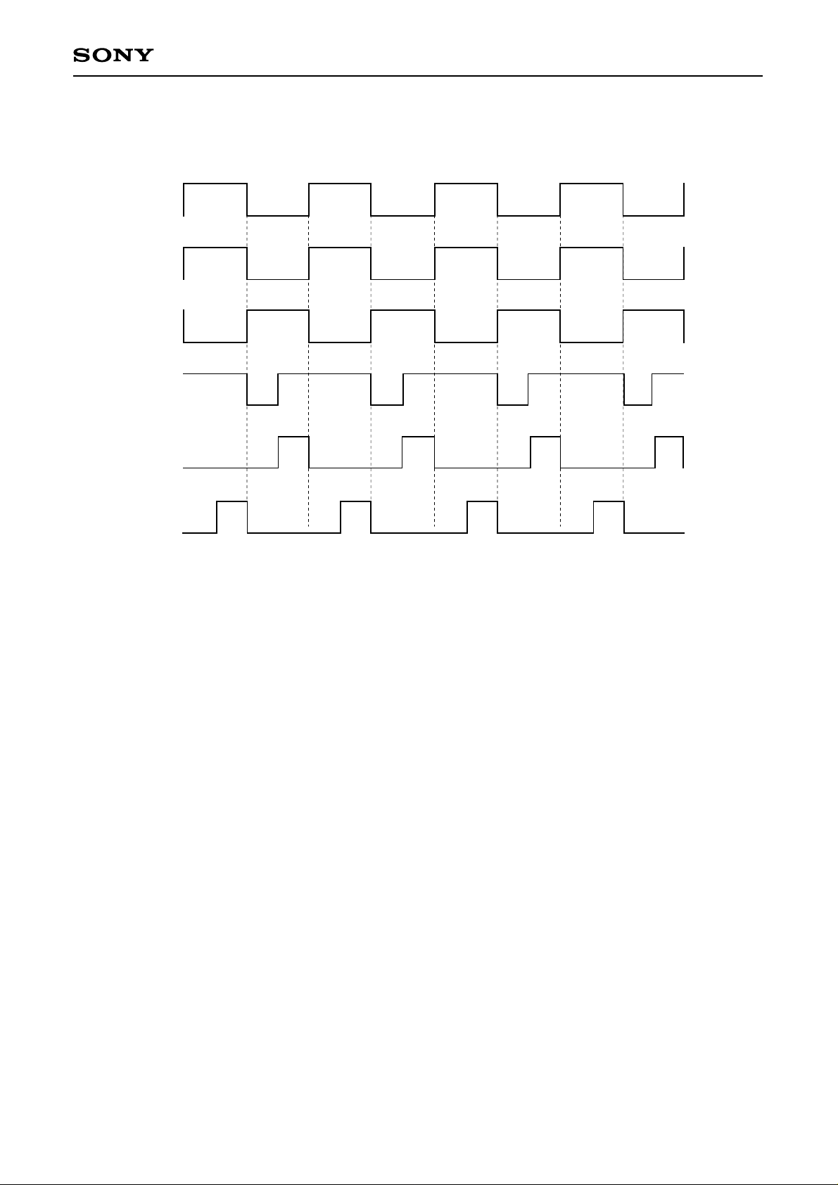
Timing Chart (8) High-speed pulse timing
CLK
XH1
XH2
XRG
SHP
CXD2422R
SHD
– 21 –
Page 22
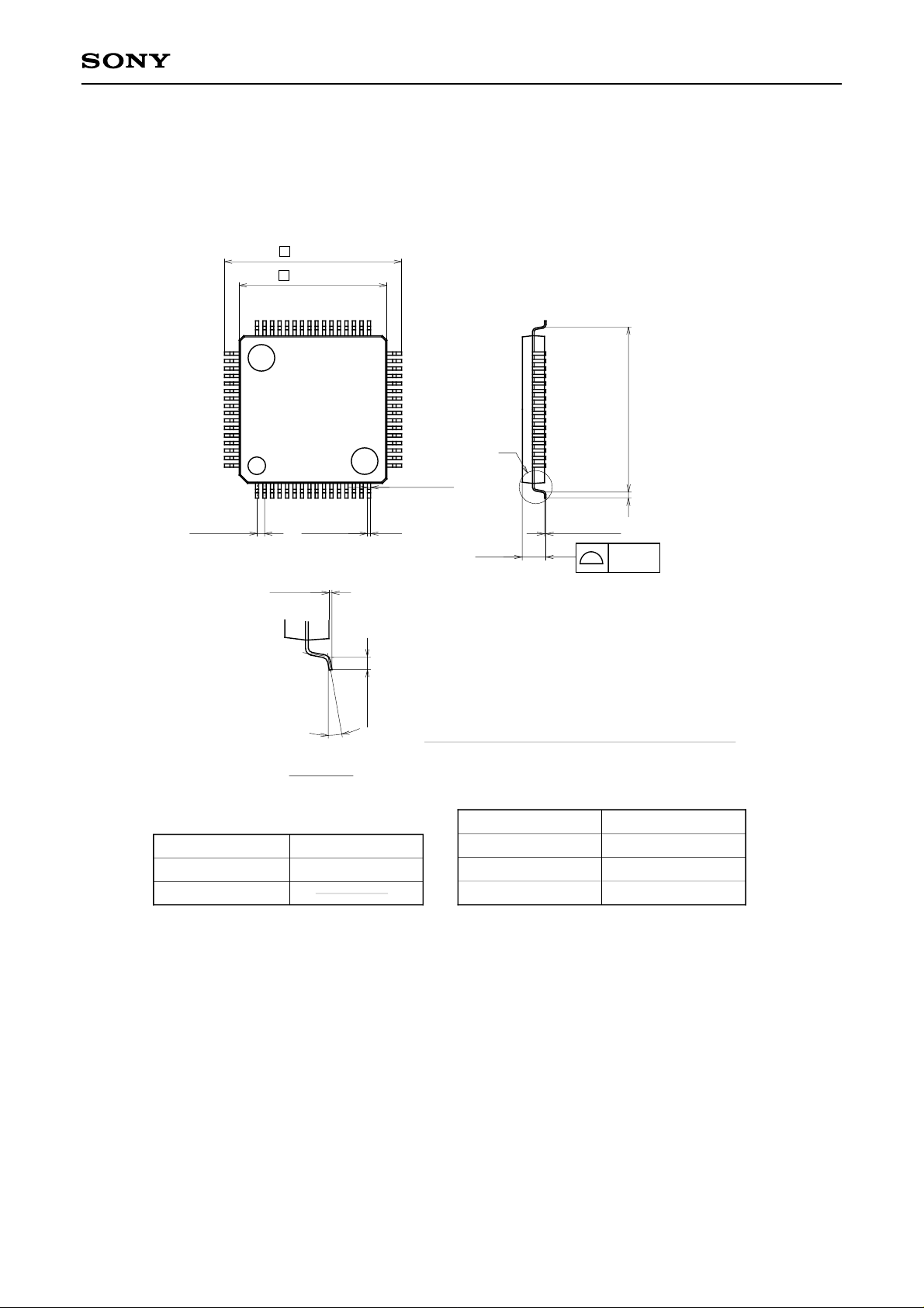
Package Outline Unit: mm
12.0 ± 0.2
∗ 10.0 ± 0.1
CXD2422R
64PIN LQFP (PLASTIC)
49
64
0.5 ± 0.08
48
1
0° to 10°
0.18 – 0.03
0.1 ± 0.1
+ 0.08
33
0.5 ± 0.2
16
32
(11.0)
A
17
(0.22)
0.5 ± 0.2
+ 0.05
+ 0.2
1.5 – 0.1
0.127 – 0.02
0.1
NOTE: Dimension “∗” does not include mold protrusion.
SONY CODE
EIAJ CODE
JEDEC CODE
DETAIL A
LQFP-64P-L01
∗QFP064-P-1010-A
PACKAGE STRUCTURE
PACKAGE MATERIAL
LEAD TREATMENT
LEAD MATERIAL
PACKAGE WEIGHT
EPOXY / PHENOL RESIN
SOLDER PLATING
42 ALLOY
0.3g
– 22 –
 Loading...