

Page 1

Description
The CXD2411AR is a timing signal generator for
color LCD panel drivers.
Features
• Generates the LCX005BK/BKB and
LCX009AK/AKB drive pulse.
• Supports right/left inverse display.
• Supports 16:9 wide display.
• Supports CSYNC and Separate SYNC (XHD, XVD)
input.
• Supports line inversion and field inversion.
• AC drive for LCD panel during no signal
(NTSC/PAL).
• Generates timing signal of external sample-andhold circuit.
• AFC circuit supporting static and dynamic
fluctuations.
Applications
• Color LCD viewfinder
• Single-panel and three-panel projectors
Structure
Silicon gate CMOS IC
Absolute Maximum Ratings (Ta = 25°C)
• Supply voltage VDD VSS – 0.5 to +7.0 V
• Input voltage VI VSS – 0.5 to VDD + 0.5 V
• Output voltage VO VSS – 0.5 to VDD + 0.5 V
• Operating temperature
Topr –20 to +85 °C
• Storage temperature
Tstg –55 to +150 °C
Recommended Operating Conditions
• Supply voltage VDD 2.7 to 5.5 V
• Operating temperature
Topr –20 to +85 °C
– 1 –
CXD2411AR
E95Z14-ST
Timing Generator for Color LCD Panels
Sony reserves the right to change products and specifications without prior notice. This information does not convey any license by
any implication or otherwise under any patents or other right. Application circuits shown, if any, are typical examples illustrating the
operation of the devices. Sony cannot assume responsibility for any problems arising out of the use of these circuits.
48 pin LQFP (Plastic)
For the availability of this product, please contact the sales office.
Page 2
– 2 –
CXD2411AR
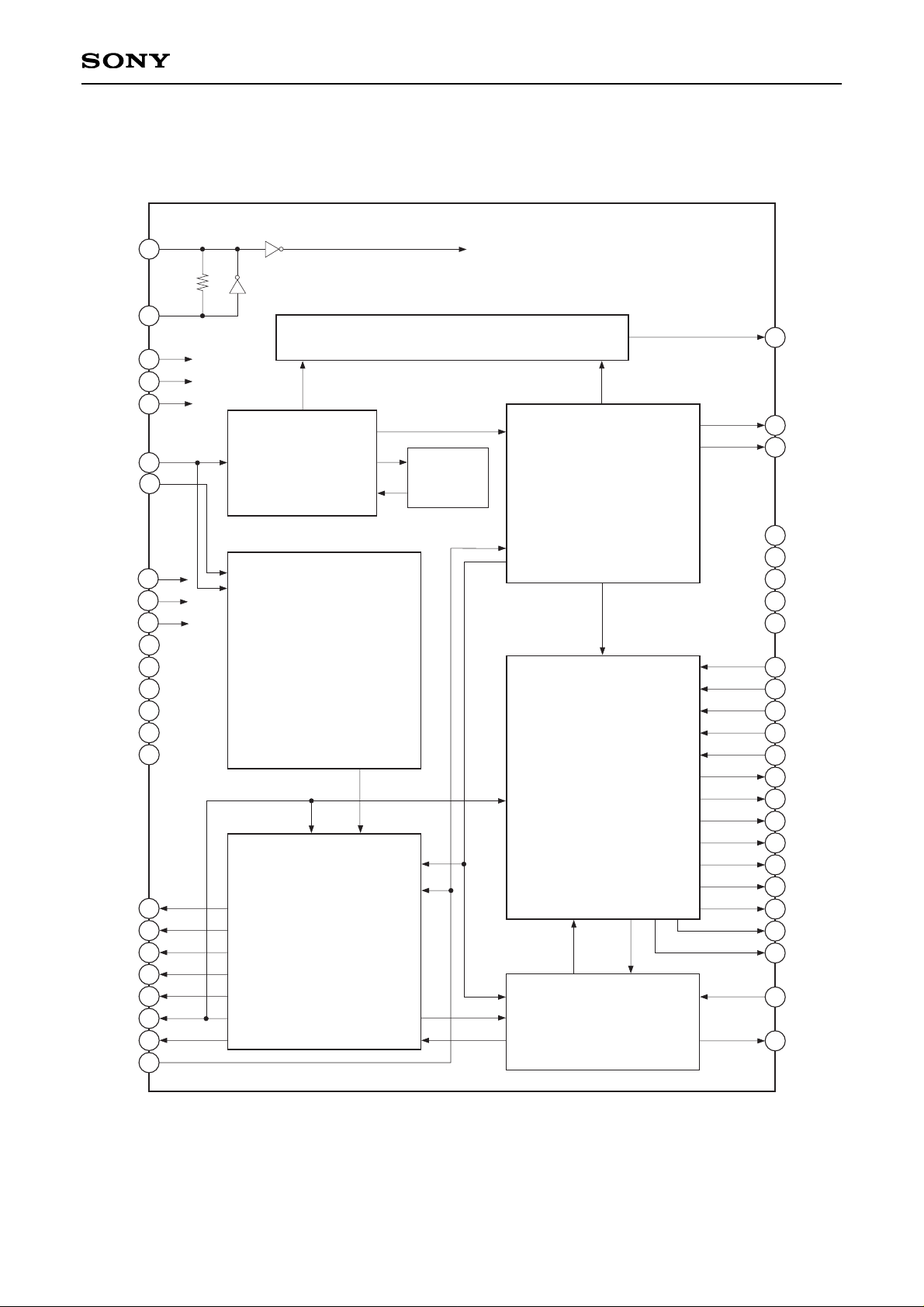
Block Diagram and Pin Configuration
PLL PHASE COMPARATOR
H-SYNC
DETECTOR
H-SKEW
DETECTOR
V-SYNC
SEPERATOR
(NOISE SHAPE)
V-TIMING
PULSE GENERATOR
PLL-COUNTER
HALF-H
KILLER
H-TIMING
PULSE
GENERATOR
26
CKO
XCLR
TST3
SLCK
XHD
CKI
PLNT
TST4
TST5
TST6
TST7
TST8
EN
VD
VST
VCK1
VCK2
FLDO
SBLK
WIDE
RPD
V
SS
HD
XCLP
V
DD
VSS
VDD
VSS
HP1
HST1
HP2
HP3
HP4
RGT
HST2
HCK1
HCK2
SH1
SH2
SH3
SH4
CLR
SLFR
FRP
master ck
FIELD & LINE
CONTROLLER
2
3
4
5
11
12
15
17
18
20
21
25
27
29
37
41
42
44
1
PAL PULSE
ELIMINATOR
6
10
13
14
16
19
22
23
24
28
30
40
39
38
36
35
34
31
32
33
43
46
47
48
TST0
TST1
TST2
7
8
9
45
XVD
Page 3
– 3 –
CXD2411AR
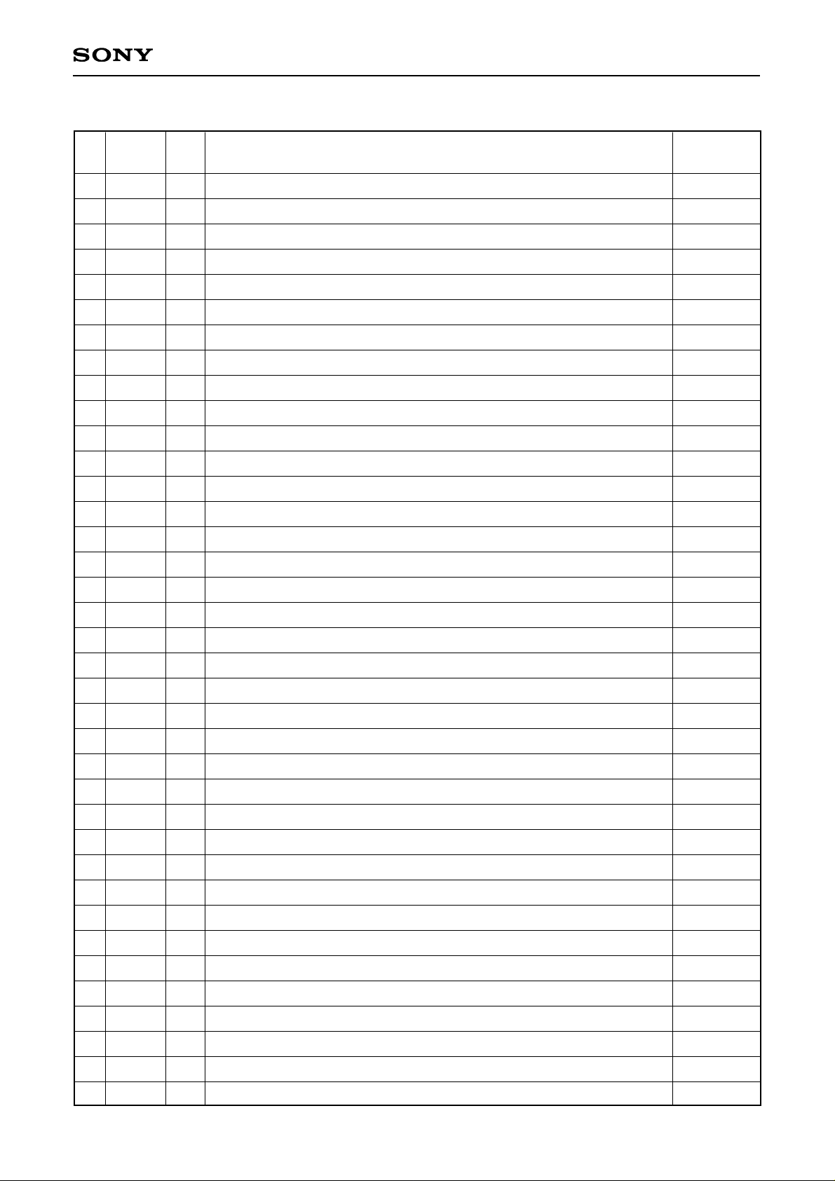
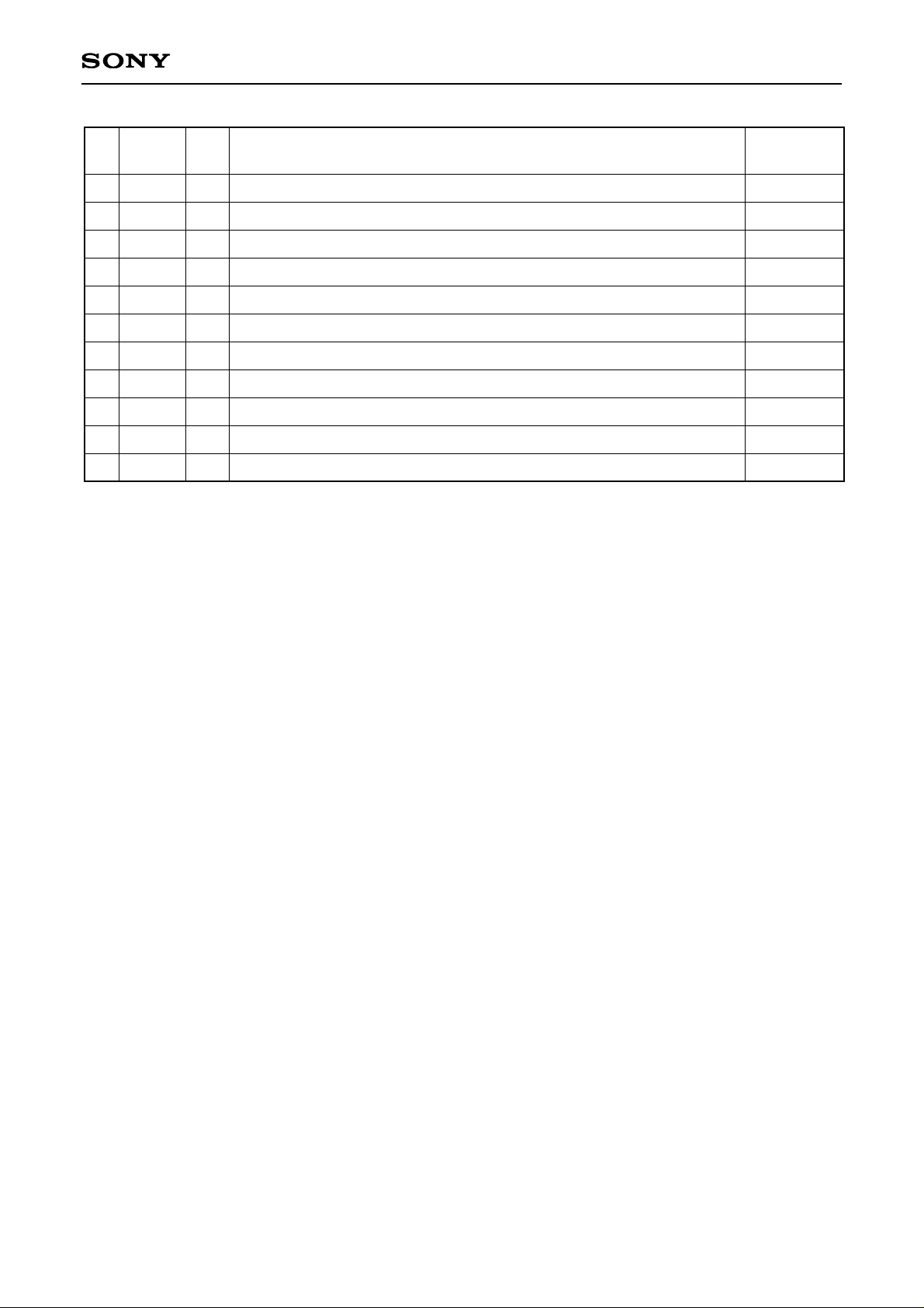
Pin Description
Pin
No.
Symbol I/O Description
Input pin for
open status
1
2
3
4
5
6
7
8
9
10
11
12
13
14
15
16
17
18
19
20
21
22
23
24
25
26
27
28
29
30
31
32
33
34
35
36
37
SLCK
PLNT
XCLR
WIDE
SBLK
VSS
TST0
TST1
TST2
RGT
TST3
TST4
SLFR
HST2
TST5
CLR
EN
VST
VDD
VCK2
VCK1
HST1
HCK2
HCK1
VD
TST6
XHD
FRP
FLDO
SH4
VSS
SH1
SH2
SH3
XCLP
HD
TST7
I
I
I
I
O
—
—
—
—
I
—
—
I
O
—
O
O
O
—
O
O
O
O
O
O
—
I
O
O
O
—
O
O
O
O
O
—
Switches between LCX005BK (H) and LCX009 (L)
Switches between PAL (H) and NTSC (L)
Cleared at 0V
Switches between 16:9 display (H) and 4:3 display (L)
Black signal pulse output (during WIDE MODE) (positive polarity)
GND
Leave this open.
Leave this open.
Leave this open.
Switches between Normal scan (H) and Reverse scan (L)
Leave this open.
Leave this open.
Switches between field inversion (H) and line inversion (L)
H start pulse 2 (positive polarity)
Leave this open.
CLR pulse output (positive polarity)
EN pulse output (negative polarity)
V start pulse (positive polarity)
Power supply
V clock pulse 2
V clock pulse 1
H start pulse 1 (positive polarity)
H clock pulse 2
H clock pulse 1
VD pulse output (positive polarity)
Leave this open.
XHD (negative polarity)/Composite sync (positive polarity) input
AC drive timing pulse output
Field identification signal output
Sample-and-hold pulse (positive polarity)
GND
Sample-and-hold pulse (positive polarity)
Sample-and-hold pulse (positive polarity)
Sample-and-hold pulse (positive polarity)
Burst position clamp pulse output (negative polarity)
HD pulse output (positive polarity)
Leave this open.
L
L
H
L
—
—
—
—
H
—
—
L
—
—
—
—
—
—
—
—
—
—
—
—
—
—
—
—
—
—
—
—
—
—
Page 4
– 4 –
CXD2411AR
38
39
40
41
42
43
44
45
46
47
48
HP4
RPD
VSS
CKO
CKI
VDD
TST8
XVD
HP1
HP2
HP3
I
O
—
O
I
—
—
I
I
I
I
Switches for the horizontal display position
Phase comparator output
GND
Oscillation cell (output)
Oscillation cell (input)
Power supply
Leave this open.
XVD (negative polarity) input
Switches for the horizontal display position
Switches for the horizontal display position
Switches for the horizontal display position
H
—
—
—
—
L
L
L
L
(H: Pull up, L: Pull down)
Note) The CXD2411AR processes CSYNC and Separate SYNC inputs with the same pins. Therefore, care
should be given to the following points when using the CXD2411AR.
1) During CSYNC input, the XVD input pin should be set to L or left open.
2) During Separate SYNC input (XHD, XVD), the XVD width specification is from 2H to 10H.
Pin
No.
Symbol I/O Description
Input pin for
open status
Page 5
– 5 –
CXD2411AR
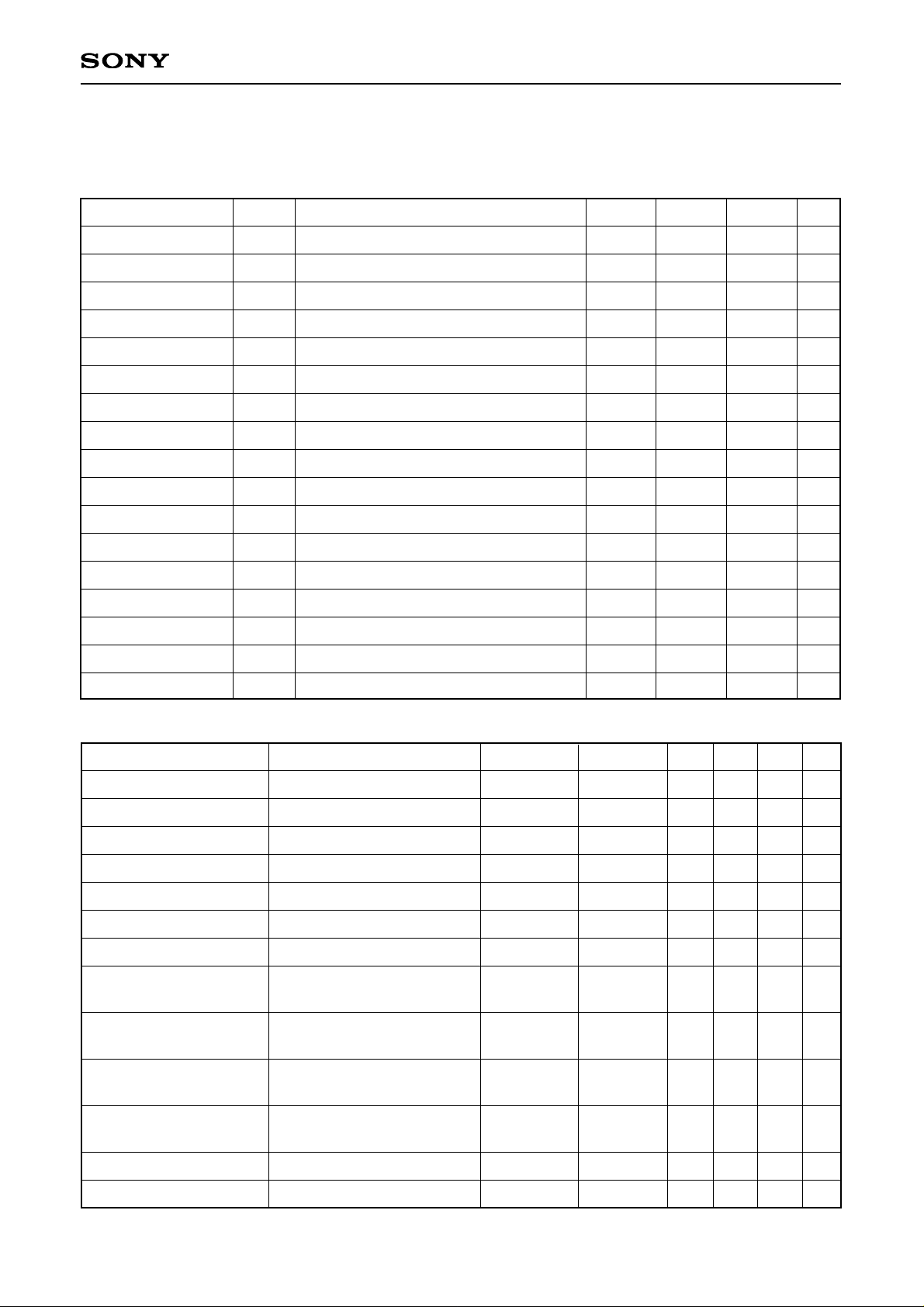
Electrical Characteristics
1. DC characteristics (Temperature = 25°C, VSS = 0V)
Item Symbol Min. Typ. Max. UnitConditions
Supply voltage
Input voltage
Input voltage
Input voltage
Input voltage
Input voltage
Output voltage
Output voltage
Output voltage
Output voltage
Output voltage
Output voltage
Input leak current
Input leak current
Input leak current
Output leak current
Current consumption
VDD
VIH
VIH
VIL
VIH
VIL
VOH
VOL
VOH
VOL
VOH
VOL
IL
IIL
IIH
ILZ
IDD
TTL input cell (5V ±10%)
TTL input cell (3.0V ±10%)
TTL input cell
CMOS input cell
CMOS input cell
IOH = –4mA (HCKn, VCKn)
IOL = 8mA (HCKn, VCKn)
IOH = –3mA (CKO, CKI)
IOL = 3mA (CKO, CKI)
IOH = –2mA (other than the above)
IOL = 4mA (other than the above)
Normal input pin
With pull-up resistor
With pull-down resistor
RPDn, FPDn (at high impedance state)
VDD = 5.0V
2.7
2.2
1.8
0.7VDD
VDD – 0.8
VDD/2
VDD – 0.8
–10
–12
12
–40
–100
100
25
5.5
0.8
0.3VDD
0.4
VDD/2
0.4
10
–240
240
40
V
V
V
V
V
V
V
V
V
V
V
V
µA
µA
µA
µA
mA
2. AC characteristics (VDD = 2.7 to 5.5V)
Item Applicable pins Min. Typ. Max. UnitConditions
Clock input cycle
Cross-point time difference
Cross-point time difference
Output rise delay
Output fall delay
Output rise delay
Output fall delay
HCK1, SH1 delay time
difference
HCK1, SH1 delay time
difference
HCK2, SH1 delay time
difference
HCK2, SH1 delay time
difference
HCK1 Duty
HCK2 Duty
CKI
HCK1, HCK2
VCK1, VCK2
HCKn, VCKn
HCKn, VCKn
Other than HCKn and VCKn
Other than HCKn and VCKn
HCK1, SH1
HCK1, SH1
HCK2, SH1
HCK2, SH1
HCK1
HCK2
CL = 30pF
CL = 30pF
CL = 30pF
CL = 30pF
CL = 30pF
CL = 30pF
CL = 30pF
CL = 30pF
CL = 30pF
CL = 30pF
CL = 30pF
CL = 30pF
60
60
60
60
60
46
46
10
10
30
25
40
22
85
95
85
95
52
52
ns
ns
ns
ns
ns
ns
ns
ns
ns
ns
ns
%
%
Symbol
∆t
∆t
tpr
tpf
tpr
tpf
dt1
dt2
dt1
dt2
tH/tH + tL
tH/tH + tL
Note) n = 1, 2
Page 6
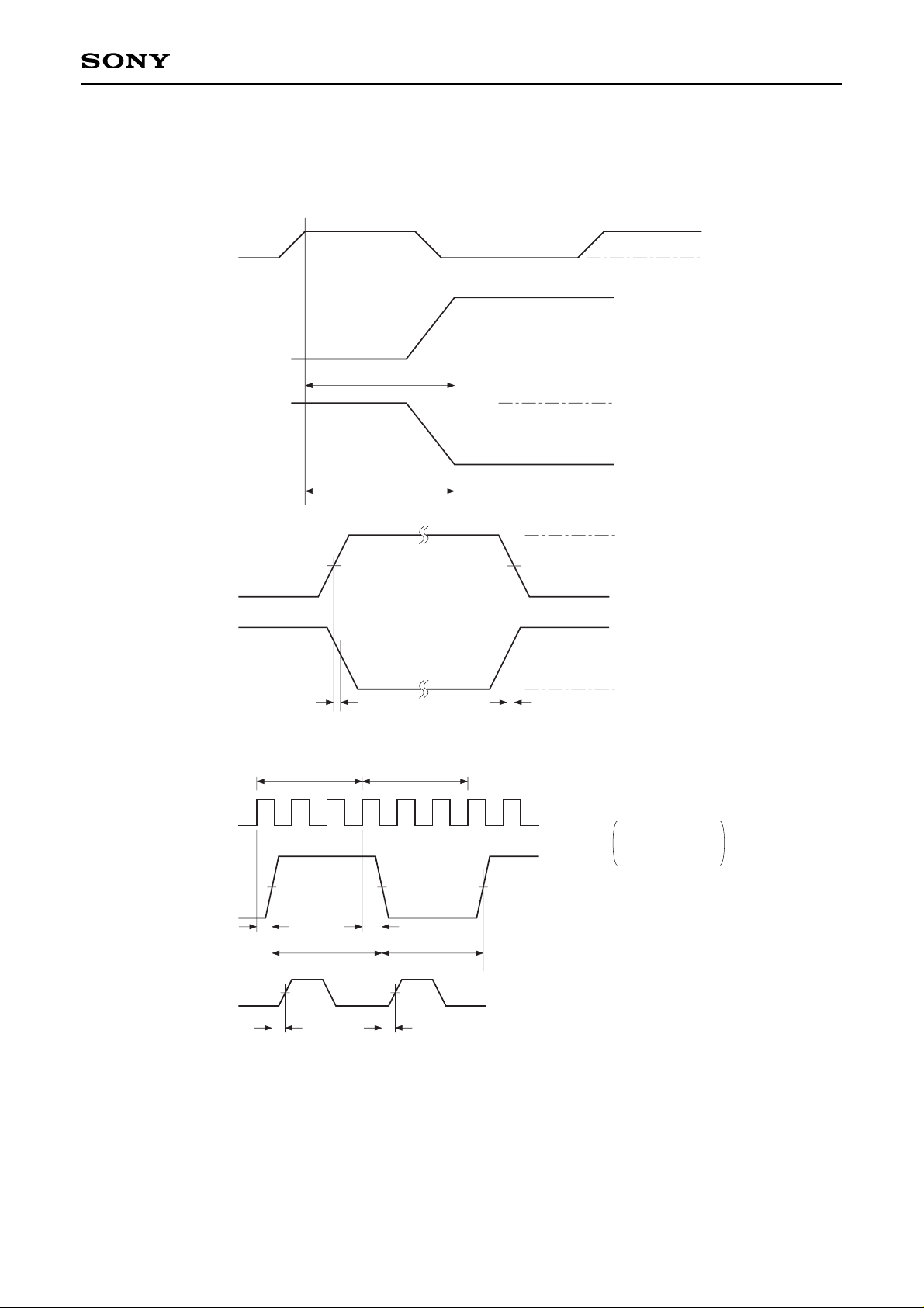
– 6 –
CXD2411AR
tpr
tpf
Output
Output
CKI
V
DD
0V
V
DD
0V
V
DD
0V
t t
50% 50% 50%
tH tL
t2t1
50% 50%
dt1 dt2
CKI
SH1
t
H – tL = 2 (t – t1)
t
H = t – t1 + t2
tL = t – t2 + t1
tH – tL = 2 (t2 – t1)
50%
50% 50%
50%
∆t∆t
VDD
0V
V
DD
0V
VCK1
(HCK1)
VCK2
(HCK2)
HCK1
(HCK2)
Timing Definition
Page 7
– 7 –
CXD2411AR
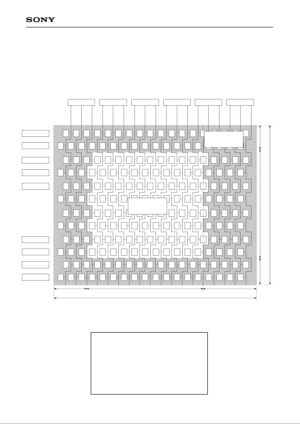
LCX005BK/BKB and LCX009AK/AKB Color Coding Diagram
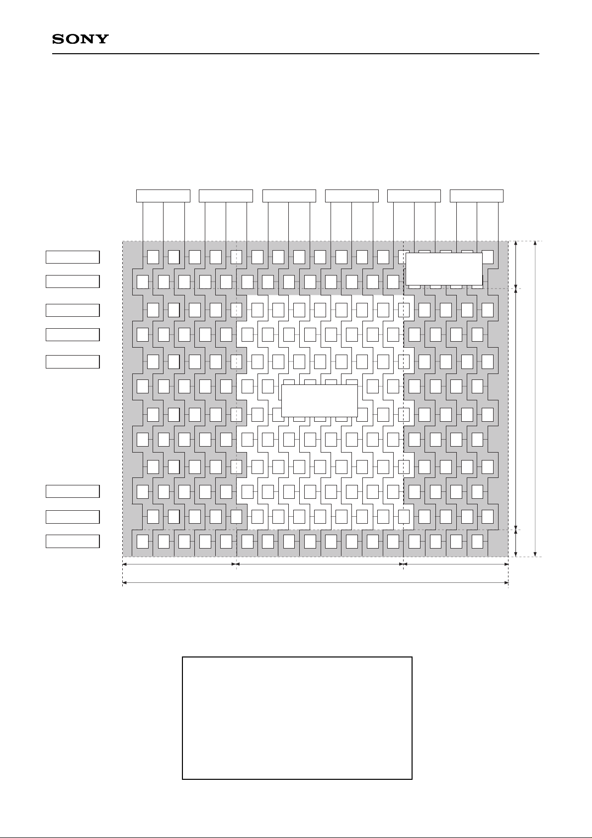
The delta arrangement is used for the color coding in the LCD panels with which this IC is compatible. Note
that the shaded region within the diagram is not displayed.
LCX005BK/BKB pixel arrangement
R G B R G B R G B R G B R G B R
GRBGRBGRBGRBGRBG
R G B R G B R G B R G B R G B R
GRBGRBGRBGRBGRBG
R G B R G B R G B R G B R G B R
GRBGRBGRBGRBGRBG
R G B R G B R G B R G B R G B R
GRBGRBGRBGRBGRBG
R G B R G B R G B R G B R G B R
RBGRBGRBGRBGRBG
B
R
B
R
B
R
B
R
B
R
G
HSW1 dummy2 to 5
HSW2 HSW3 HSW174 HSW175
Display area
Photo-shielding area
537
3 521 13
2
2
218
222
G
B
G
B
G
B
G
B
G
B
R G B R G B R G B R G B R G B R
RBGRBGRBGRBGRBG
B
R
G
G
B
dummy1
dummy2
Vline1
Vline2
Vline3
Vline217
Vline218
dummy3
dummy4
Basic specifications
Total horizontal dots : 537H
Horizontal display dots : 521H
Total vertical dots : 222H
Vertical display dots : 218H
Total dots : 119,214H
Display dots : 113,578H
Page 8
– 8 –
CXD2411AR
LCX009AK/AKB pixel arrangement
R G B R G B R G B R G B R G B R
GRBGRBGRBGRBGRBG
R G B R G B R G B R G B R G B R
GRBGRBGRBGRBGRBG
R G B R G B R G B R G B R G B R
GRBGRBGRBGRBGRBG
R G B R G B R G B R G B R G B R
GRBGRBGRBGRBGRBG
R G B R G B R G B R G B R G B R
RBGRBGRBGRBGRBG
B
R
B
R
B
R
B
R
B
R
G
dummy1 to 4 dummy5 to 8
HSW1 HSW2 HSW267 HSW268
Display area
Photo-shielding area
827
14 800 13
2
1
225
228
R G B R G B R G B R G B R G B R
RBGRBGRBGRBGRBG
B
R
G
dummy1
dummy2
Vline1
Vline2
Vline3
Vline224
Vline225
dummy3
Basic specifications
Total horizontal dots : 827H
Horizontal display dots : 800H
Total vertical dots : 228H
Vertical display dots : 225H
Total dots : 188,556H
Display dots : 180,000H
Page 9
– 9 –
CXD2411AR
Description of Mode Selection Switch (SLCK, PLNT, WIDE)
SLCK PLNT
MODE
H
H
H
H
L
L
L
L
L
L
H
H
L
L
H
H
WIDE
L
H
L
H
L
H
L
H
LCX005BK/BKB, NTSC, NORMAL
LCX005BK/BKB, NTSC, WIDE
LCX005BK/BKB, PAL, NORMAL
LCX005BK/BKB, PAL, WIDE
LCX009AK/AKB, NTSC, NORMAL
LCX009AK/AKB, NTSC, WIDE
LCX009AK/AKB, PAL, NORMAL
LCX009AK/AKB, PAL, WIDE
∗
NORMAL (4:3 display), WIDE (16:9 display)
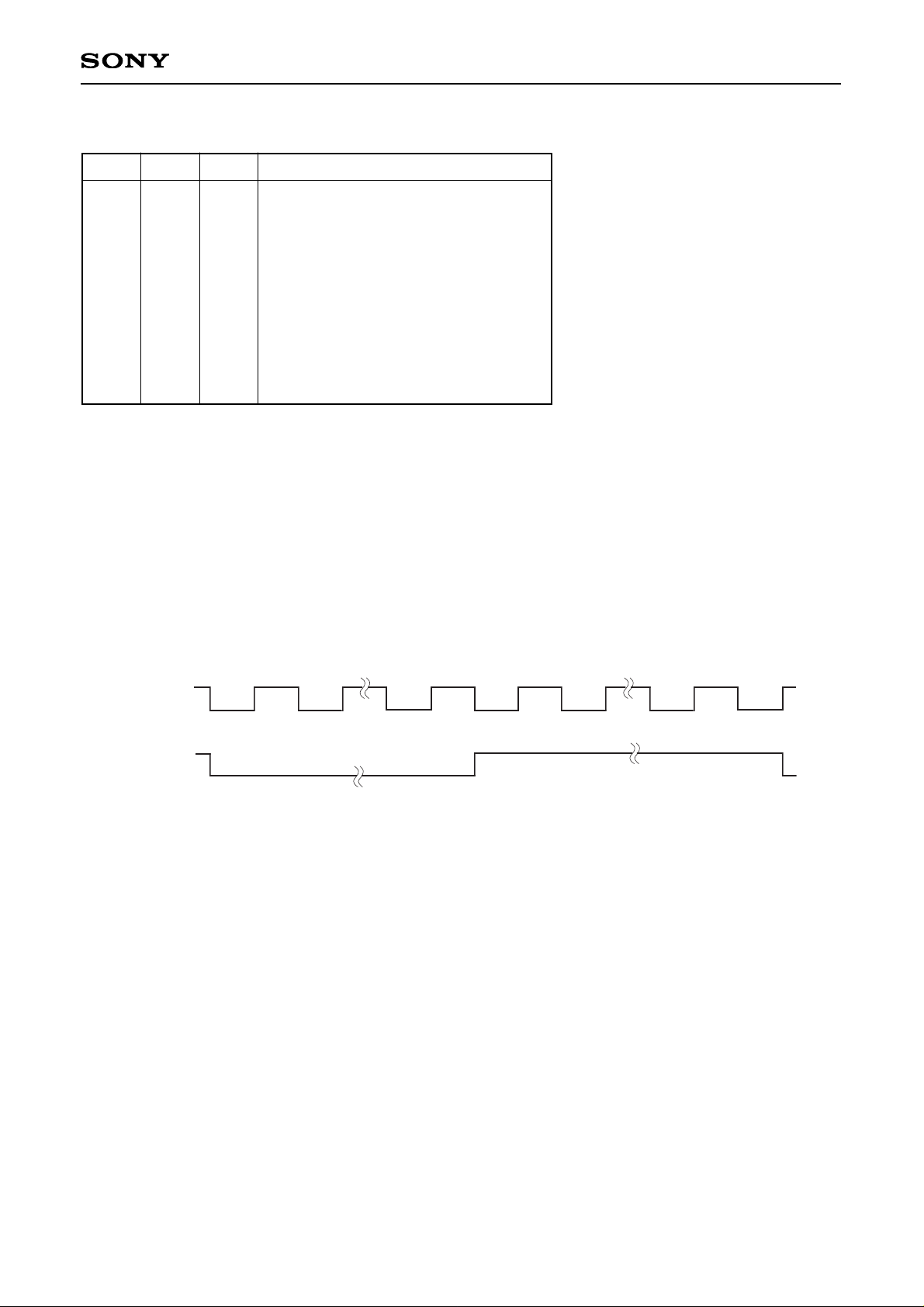
SLFR
SLFR is the selector switch for the AC drive timing pulse (FRP). This switch selects field inversion when H and
line inversion when L. Normally, line inversion (L) is used. The transition point is one clock cycle after the
transition point of the VCK1 and VCK2 pulses.
1H
1Field
1Field
1H
1H inversion
(2H cycle)
1F inversion
(2F cycle)
∗
FRP polarity is not specified.
FRP
1H 1H
Page 10
– 10 –
CXD2411AR
HP1, 2, 3, 4
These are selector switches for the horizontal display position. The HST timing can be set at 2fh intervals in 16
different ways by using the four HST position bits. The picture center is set at internal preset value: HP1/2/3/4:
LLLH. However, actually, because there is a difference between the RGB signal and the drive pulse delays,
the picture center may not match the design center. In this case, adjust with these switches.
The HST timing (from SYNC termination to the rising edge of HST) for even lines is shown below.
LCX005BK/BKB (NTSC, PAL)
0
0
0
0
0
0
0
0
1
1
1
1
1
1
1
1
0
0
0
0
1
1
1
1
0
0
0
0
1
1
1
1
0
0
1
1
0
0
1
1
0
0
1
1
0
0
1
1
0
1
0
1
0
1
0
1
0
1
0
1
0
1
0
1
72fh (6.51/6.56µs)
70fh
68fh
66fh
64fh
62fh
60fh
58fh
56fh (5.06/5.11µs)
54fh
52fh
50fh
48fh
46fh
44fh
42fh (3.80/3.83µs)
74.5fh (6.74/6.79µs)
72.5fh
70.5fh
68.5fh
66.5fh
64.5fh
62.5fh
60.5fh
58.5fh (5.29/5.33µs)
56.5fh
54.5fh
52.5fh
50.5fh
48.5fh
46.5fh
44.5fh (4.02/4.06µs)
HP4 HP3 HP2 HP1
HST1 (NTSC/PAL) HST2 (NTSC/PAL)
∗
The HST1 and 2 timing for odd lines is 1.5fh delayed and 1.5fh advanced respectively from the above
timings. (Refer to the Timing Charts for details.)
Page 11
– 11 –
CXD2411AR
LCX009AK/AKB (NTSC, PAL)
0
0
0
0
0
0
0
0
1
1
1
1
1
1
1
1
0
0
0
0
1
1
1
1
0
0
0
0
1
1
1
1
0
0
1
1
0
0
1
1
0
0
1
1
0
0
1
1
0
1
0
1
0
1
0
1
0
1
0
1
0
1
0
1
91fh (5.51/5.55µs)
89fh
87fh
85fh
83fh
81fh
79fh
77fh
75fh (4.54/4.57µs)
73fh
71fh
69fh
67fh
65fh
63fh
61fh (3.69/3.72µs)
93.5fh (5.66/5.70µs)
91.5fh
89.5fh
87.5fh
85.5fh
83.5fh
81.5fh
79.5fh
77.5fh (4.69/4.72µs)
75.5fh
73.5fh
71.5fh
69.5fh
67.5fh
65.5fh
63.5fh (3.84/3.87µs)
HP4 HP3 HP2 HP1
HST1 (NTSC/PAL) HST2 (NTSC/PAL)
∗
The HST1 and 2 timing for odd lines is 1.5fh delayed and 1.5fh advanced respectively from the above
timings. (Refer to the Timing Charts for details.)
Page 12
– 12 –
CXD2411AR
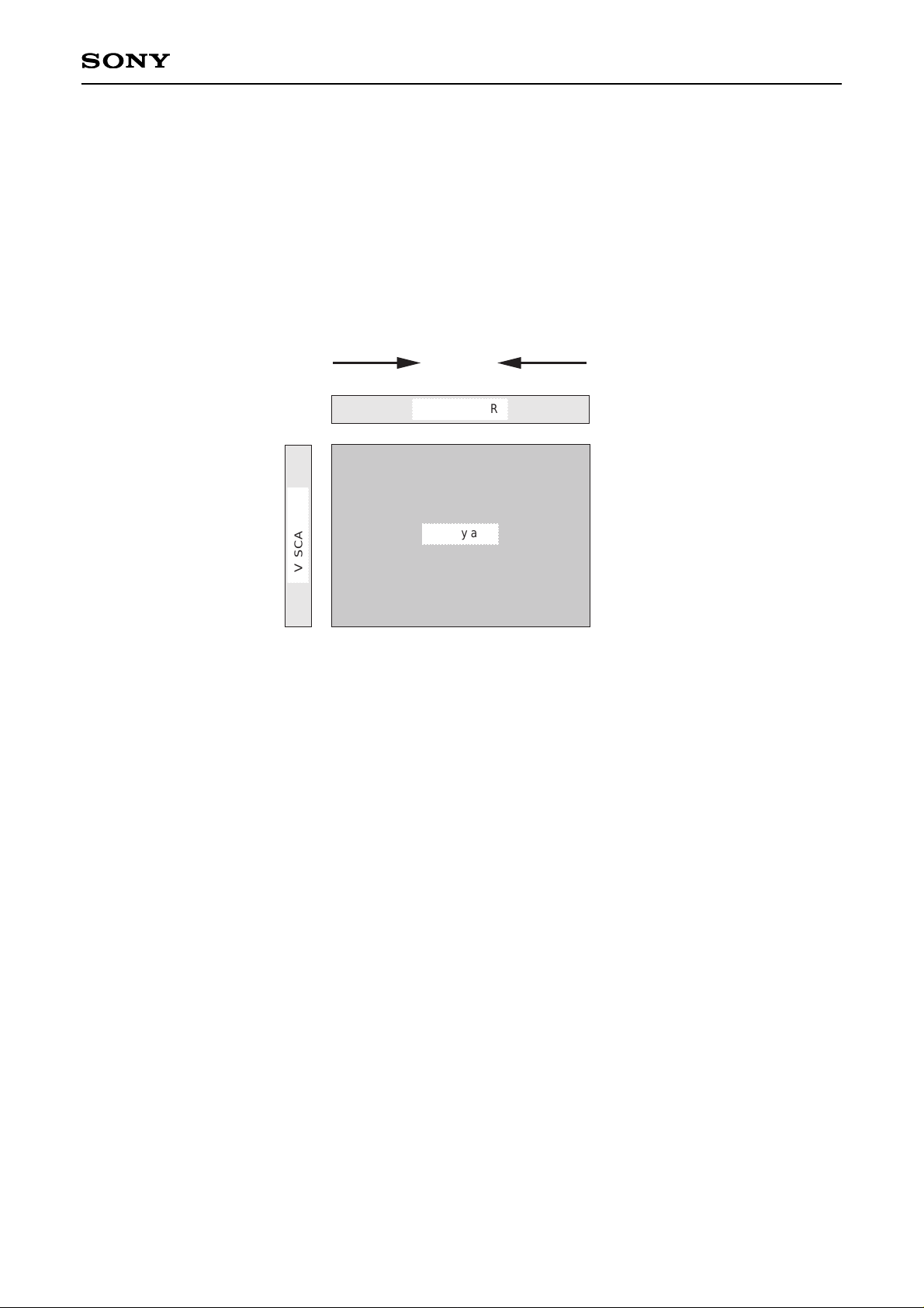
Right/Left Inversion
The LCD panel is arranged in a delta pattern, where identical signal line has 1.5-dot offset at adjoining vertical
lines. For this reason, a 1.5-bit offset is attached to the horizontal start pulse (HST) between odd lines and
even lines. HCK and SH are also 1.5-bit offset in a similar manner.
When the panel is driven with left scan (Reverse scan), this offset relationship becomes inverted for even and
odd lines. Moreover, since the dot arrangement is asymmetrical, the HST position is also changed. The
CXD2411AR deals with this inversion as follows.
When using single-panel
(1) When the right/left inversed-identification pin (RGT) goes L, the relationship concerning HCK output
switches between odd and even lines. In this case, use HST1 for the horizontal direction start pulse.
When RGT is H:
Right scan mode is on. The right scan drive pulse is output by the timing generator and is supplied to
the panel.
When RGT is L:
Left scan mode is on. The left scan drive pulse is output by the timing generator and is supplied to the
panel.
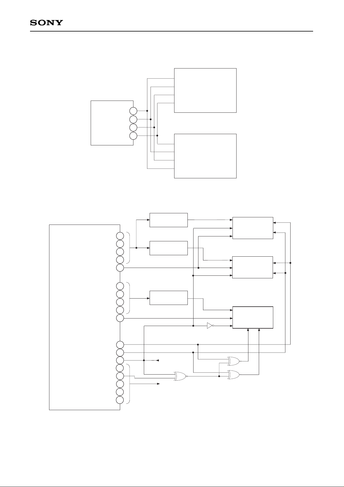
When using three-panels
(1) In order to be able to simultaneously drive three panels, with a mixture of right/left inversion on and off,
output two pulses regarding HST pulse: HST1 for right scan (Normal scan) and HST2 for left scan
(Reverse scan).
In addition, left and right scan outputs are necessary for the RGT signal as well. However, since this timing
generator does not have an RGT (right/left inversed-identification) output pin for left scan, external
measures must be taken. Similarly, external measures are also taken for HCK1 and 2.
Regarding SH, the wiring of SH1 and SH4 to the driver IC.
(2) When the right/left inversed-identification pin (RGT) goes L, the relationship concerning HCK output
switches between odd and even lines for each output switches.
When RGT is H:
Right scan mode is on. The right scan (A) and left scan (B) drive pulses are output by the timing
generator and are supplied to panels 1 and 2 and panel 3, respectively.
When RGT is L:
Left scan mode is on and (A) and (B) outputs are switched. Accordingly, panels 1 and 2 are used for
left scan and panel 3 changes to right scan.
V SCANNER
Display area
Right scan
(Normal scan)
Left scan
(Reverse scan)
H SCANNER
Page 13
– 13 –
CXD2411AR
Application Circuit (Three-panel LCD drive)
SH1
SH2
SH3
SH4
TG
SH1
SH2
SH3
SH4
SH1
SH2
SH3
SH4
Right scan driver
30
34
33
32
Left scan driver
Signal Driver
Right scan output
(A)
Panel 2
(Right scan)
Signal Driver
Panel 1
(Right scan)
(To all panels)
TG
SH1
SH2
SH3
SH4
HST1
VST
VCK1
VCK2
EN
CLR
Left scan output
(B)
Signal Driver
Panel 3
(Left scan)
RGT IN
SH1
SH2
SH3
SH4
HST2
HCK1
HCK2
RGT
(common)
32
33
34
30
22
32
33
34
30
14
24
23
10
18
21
20
17
16
∗
The facing of the three panels is the same.
Page 14
– 14 –
CXD2411AR
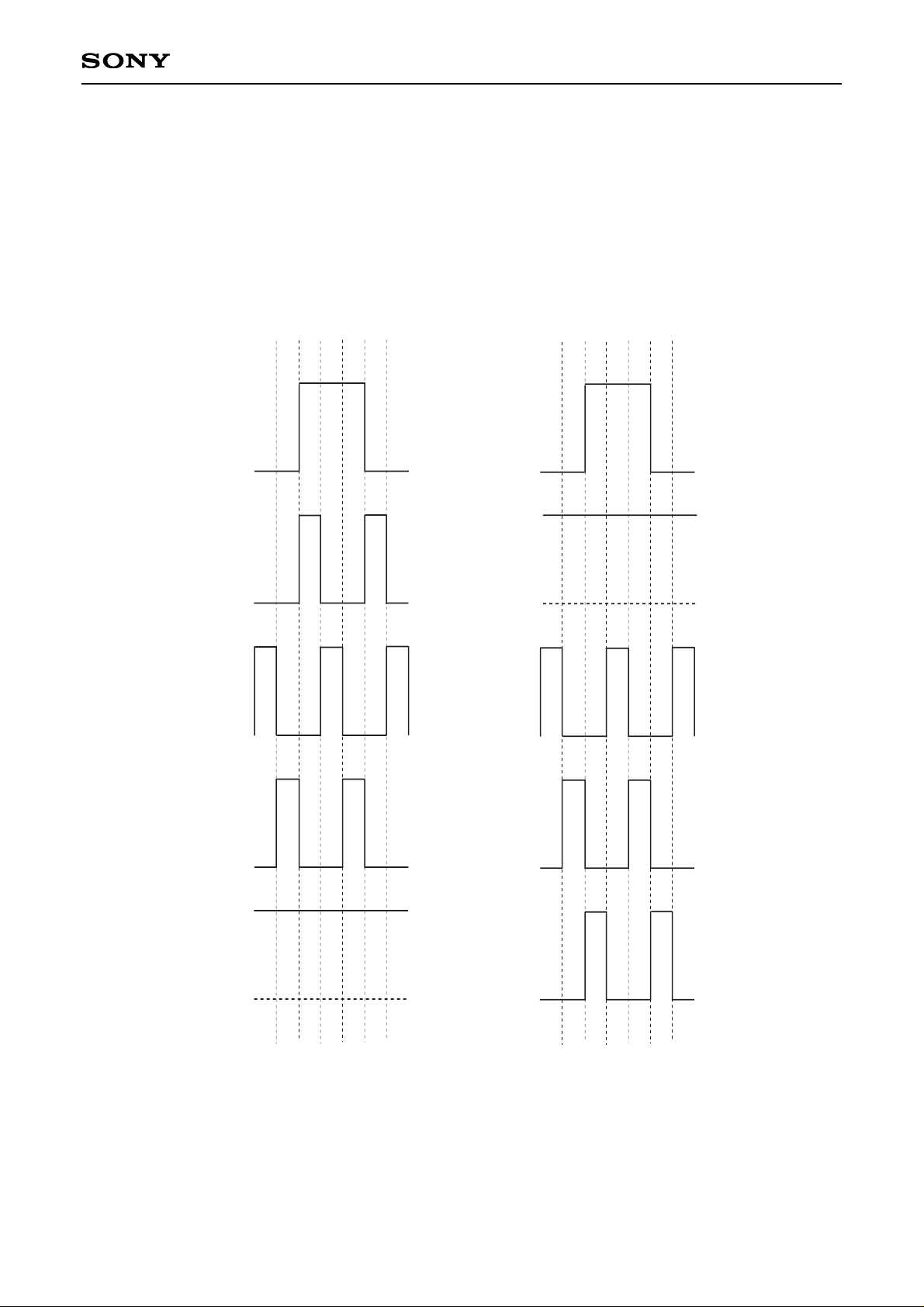
SH Pulse and HCK Phase Relationship
The phase relationship between the SH pulse and HCK changes according to switching between right scan
(Normal scan) and left scan (Reverse scan).
In the present timing, SH3 is the re-sampling pulse.
HCK1
SH1
SH2
SH3
SH4
RGT = H (Normal scan) RGT = L (Reverse scan)
Page 15
– 15 –
CXD2411AR
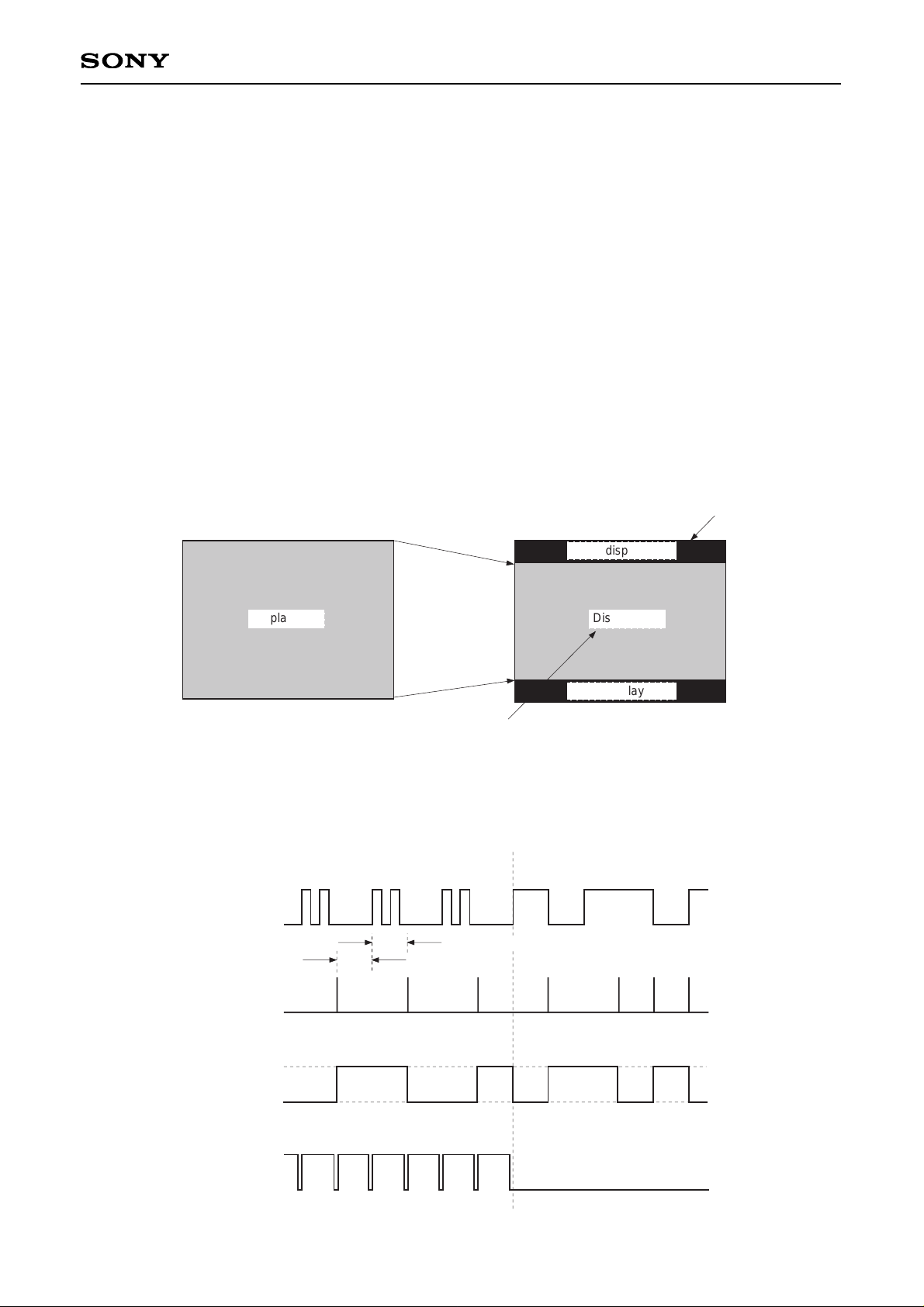
WIDE Mode
Setting the WIDE pin (Pin 4) to H, shifts the unit to WIDE mode. In this mode, the aspect ratio is converted
through pulse eliminator processing, allowing 16:9 quasi-WIDE display.
During WIDE mode, vertical pulse eliminator scanning of 1/4 for NTSC and 1/2 and 1/4 for PAL, are
performed, and the video signal is compressed to achieve a 16:9 aspect ratio. In addition, in areas outside the
display area, black is displayed by performing high-speed scanning. The timing during high-speed scanning is
a 2H cycle pulse consisting of normal drive (1H) and quadruple-speed drive (1H) and black signals are written
in 28 and 27 lines, respectively of the upper and lower side of this display area. During this time, FRP is
changed to a 4H cycle, HST to a 2H cycle, and EN and CLR are not output.
In addition, the SBLK output, which is the black signal generation timing pulse, becomes H.
(For example, black display in the panel is permitted by connecting the black signal output SBLK to the
external RGB input pin of the CXA1785R/AR.)
Refer to the attached sheets for detailed timing.
4 : 3 display
28 LINES
(28 LINES)
218 LINES
(225 LINES)
Vertical pulse eliminator scanning
(at normal-speed scanning)
Vertical high-speed scanning
16 : 9 display
Display area
163 LINES
(169 LINES)
27 LINES
(28 LINES)
Display area
Black display area
VCK1
Normal-speed scanning
2H cycle
HST
FRP
SBLK
4H cycle
At high-speed scanning
Black display area
∗
Numbers in parentheses are for the LCX009AK/AKB.
All other numbers are for the LCX005BK/BKB.
At normal-speed scanning
Quadruple-speed scanning
Page 16
– 16 –
CXD2411AR
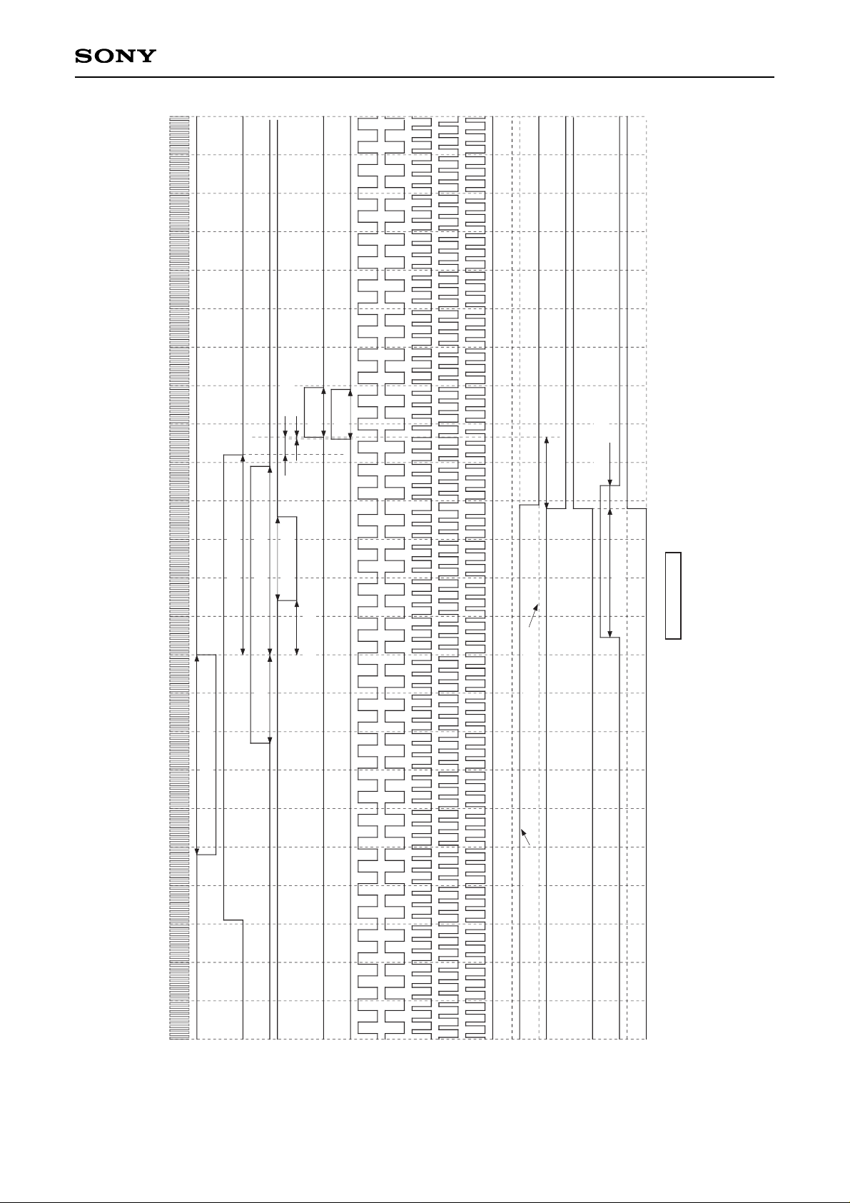
ODD LINE
Note) The third row of the timing chart "BLK" is a pulse indicated as a reference and is not a pulse output from pins.
FRP polarity is not specified for each line and field.
(BLK)
HD
XCLP
HST1
HCK2
SH1
SH3
SH2
SH4
FRP
VCK1
HST2
CLR
MCK
XHD
HCK1
VCK2
EN
HP1/2/3/4: LLLH
RGT: H (Normal scan)
4.7µs (52fh)
4.7µs (52fh)
ODD FIELD
EVEN FIELD
2.1µs (23fh) 4.4µs (49fh)
1.3µs (14fh)
2.0µs (22fh)
4.5fh
0.5fh
13fh
13fh
18.5fh
3.0µs (33fh)
0.5µs (6fh)
LCX005BK/BKB Horizontal Direction Timing Chart
NTSC/PAL
Page 17
– 17 –
CXD2411AR
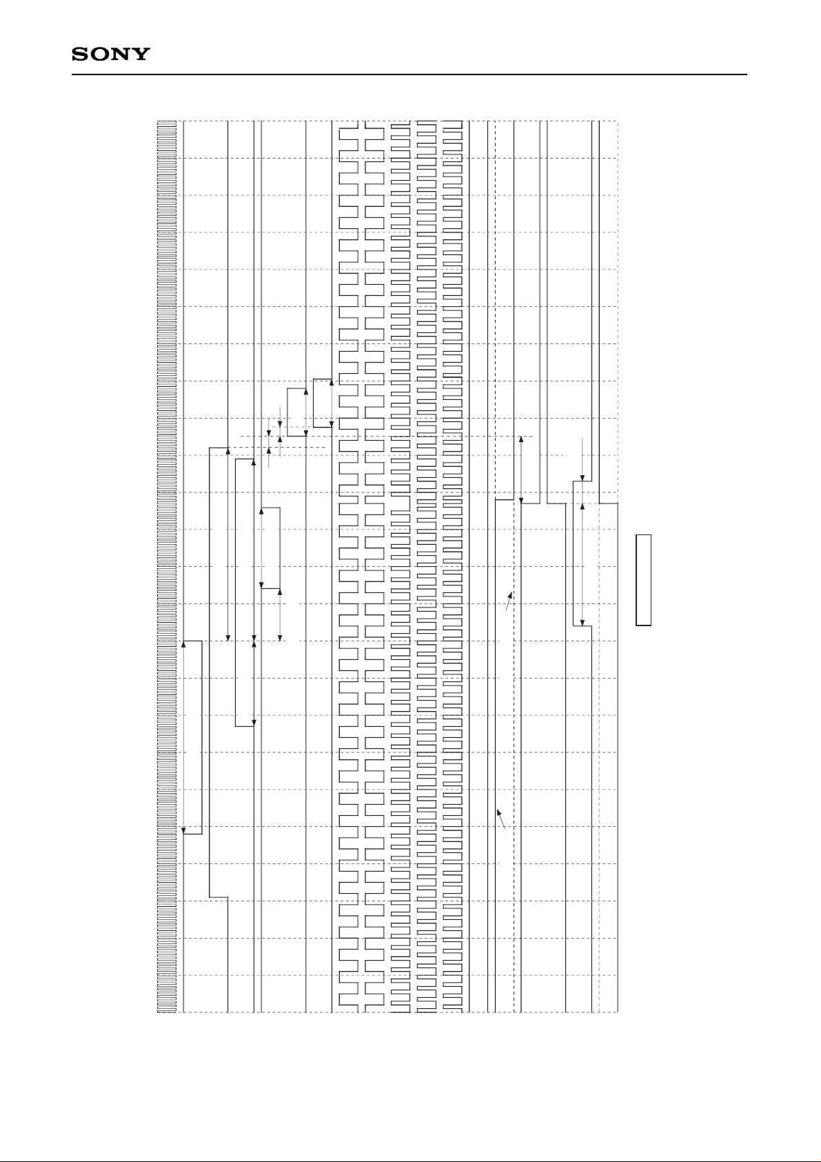
EVEN LINE
Note) The third row of the timing chart "BLK" is a pulse indicated as a reference and is not a pulse output from pins.
FRP polarity is not specified for each line and field.
(BLK)
HD
XCLP
HST1
HCK2
SH1
SH3
SH2
SH4
FRP
VCK1
HST2
CLR
MCK
HCK1
VCK2
EN
4.7µs (52fh)
4.7µs (52fh)
ODD FIELD
EVEN FIELD
2.1µs (23fh) 4.4µs (49fh)
1.3µs (14fh)
2.0µs (22fh)
3.0fh
2.5fh
13fh
13fh
18.0fh
0.5µs (6fh)
3.0µs (33fh)
XHD
HP1/2/3/4: LLLH
RGT: H (Normal scan)
LCX005BK/BKB Horizontal Direction Timing Chart
NTSC/PAL
Page 18
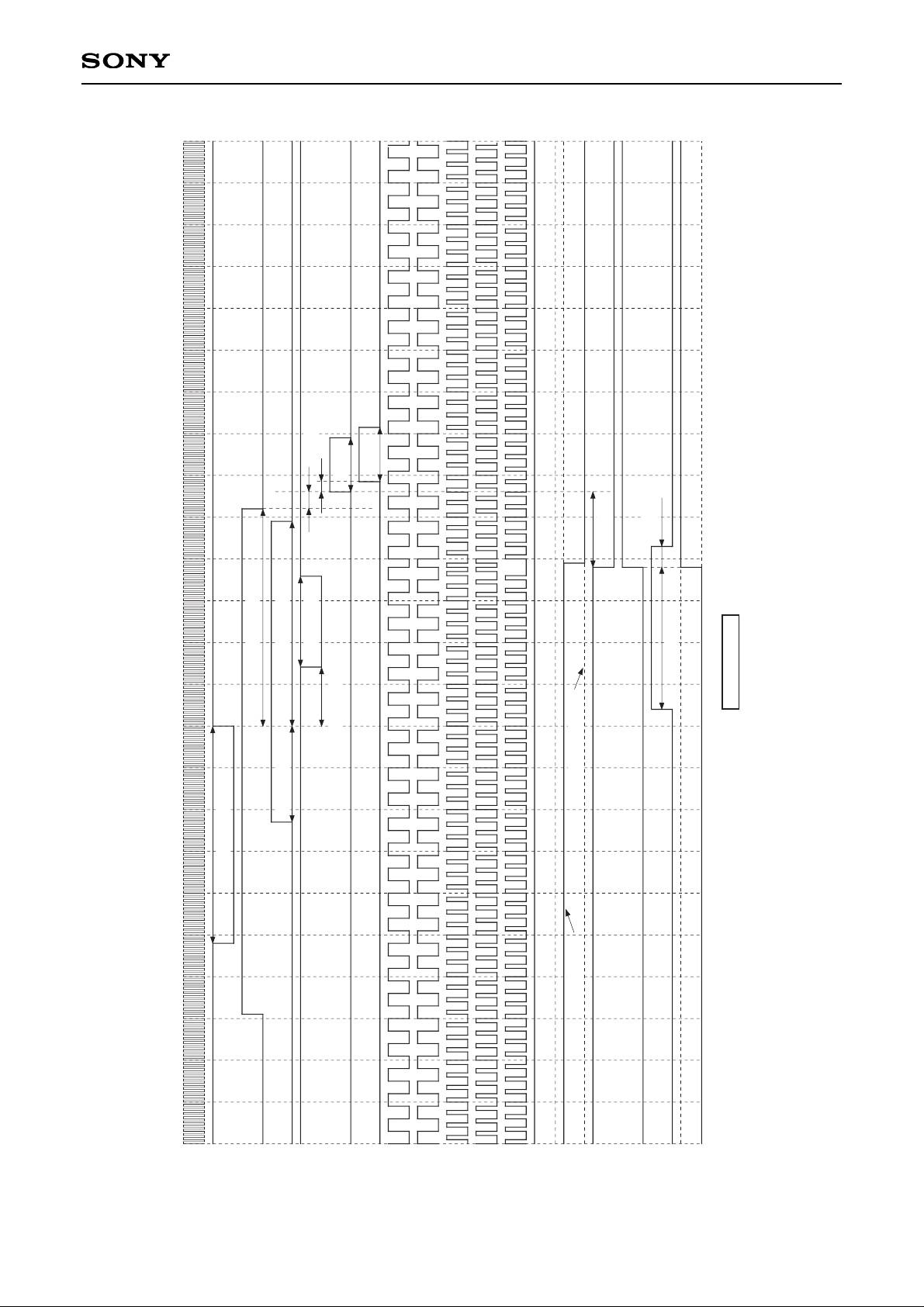
– 18 –
CXD2411AR
ODD LINE
Note) The third row of the timing chart "BLK" is a pulse indicated as a reference and is not a pulse output from pins.
FRP polarity is not specified for each line and field.
(BLK)
HD
XCLP
HST1
HCK2
SH1
SH3
SH2
SH4
FRP
VCK1
HST2
CLR
MCK
HCK1
VCK2
EN
HP1/2/3/4: LLLH
RGT: L (Reverse scan)
4.7µs (52fh)
4.7µs (52fh)
ODD FIELD
EVEN FIELD
2.1µs (23fh) 4.4µs (49fh)
1.3µs (14fh)
2.0µs (22fh)
2.5fh
4.0fh
13fh
13fh
18.0fh
0.5µs (5fh)
3.0µs (34fh)
XHD
LCX005BK/BKB Horizontal Direction Timing Chart
NTSC/PAL
Page 19

– 19 –
CXD2411AR
EVEN LINE
Note) The third row of the timing chart "BLK" is a pulse indicated as a reference and is not a pulse output from pins.
FRP polarity is not specified for each line and field.
(BLK)
HD
XCLP
HST1
HCK2
SH1
SH3
SH2
SH4
FRP
VCK1
HST2
CLR
MCK
HCK1
VCK2
EN
4.7µs (52fh)
4.7µs (52fh)
ODD FIELD
EVEN FIELD
2.0µs (22fh) 4.5µs (50fh)
1.4µs (15fh)
2.0µs (22fh)
13fh
13fh
5.5fh
0.5fh
18.5fh
0.5µs (5fh)
3.0µs (34fh)
XHD
HP1/2/3/4: LLLH
RGT: L (Reverse scan)
LCX005BK/BKB Horizontal Direction Timing Chart
NTSC/PAL
Page 20

– 20 –
CXD2411AR
ODD LINE
Note) The third row of the timing chart "BLK" is a pulse indicated as a reference and is not a pulse output from pins.
FRP polarity is not specified for each line and field.
(BLK)
HD
XCLP
HST1
HCK2
SH1
SH3
SH2
SH4
FRP
VCK1
HST2
CLR
MCK
XHD
HCK1
VCK2
EN
4.7µs (78fh)
4.7µs (78fh)
ODD FIELD
EVEN FIELD
0.5µs (8fh)
3.0µs (50fh)
12fh
12fh
2.5fh
0.5fh
2.0µs (33fh)
1.3µs (22fh)
4.4µs (72fh)
2.1µs (34fh)
43.5fh
HP1/2/3/4: LLLH
RGT: H (Normal scan)
LCX009AK/AKB Horizontal Direction Timing Chart
NTSC/PAL
Page 21

– 21 –
CXD2411AR
EVEN LINE
Note) The third row of the timing chart "BLK" is a pulse indicated as a reference and is not a pulse output from pins.
FRP polarity is not specified for each line and field.
HD
XCLP
HST1
HCK2
SH1
SH3
SH2
SH4
FRP
VCK1
HST2
CLR
MCK
XHD
HCK1
VCK2
EN
4.7µs (78fh)
4.7µs (78fh)
ODD FIELD
EVEN FIELD
2.1µs (34fh)
4.4µs (72fh)
1.3µs (22fh)
2.0µs (33fh)
2.5fh
4.0fh
12fh
12fh
43.0fh
3.0µs (50fh)
0.5µs (8fh)
HP1/2/3/4: LLLH
RGT: H (Normal scan)
(BLK)
LCX009AK/AKB Horizontal Direction Timing Chart
NTSC/PAL
Page 22

– 22 –
CXD2411AR
Note) The third row of the timing chart "BLK" is a pulse indicated as a reference and is not a pulse output from pins.
FRP polarity is not specified for each line and field.
(BLK)
HD
XCLP
HST1
HCK2
SH1
SH3
SH2
SH4
FRP
VCK1
HST2
CLR
MCK
XHD
HCK1
VCK2
EN
4.7µs (78fh)
4.7µs (78fh)
ODD FIELD
EVEN FIELD
2.1µs (34fh)
4.4µs (72fh)
1.3µs (22fh)
2.0µs (33fh)
2.5fh
3.0fh
12fh
12fh
43.0fh
3.0µs (51fh)
0.5µs (7fh)
ODD LINE
HP1/2/3/4: LLLH
RGT: L (Reverse scan)
LCX009AK/AKB Horizontal Direction Timing Chart
NTSC/PAL
Page 23
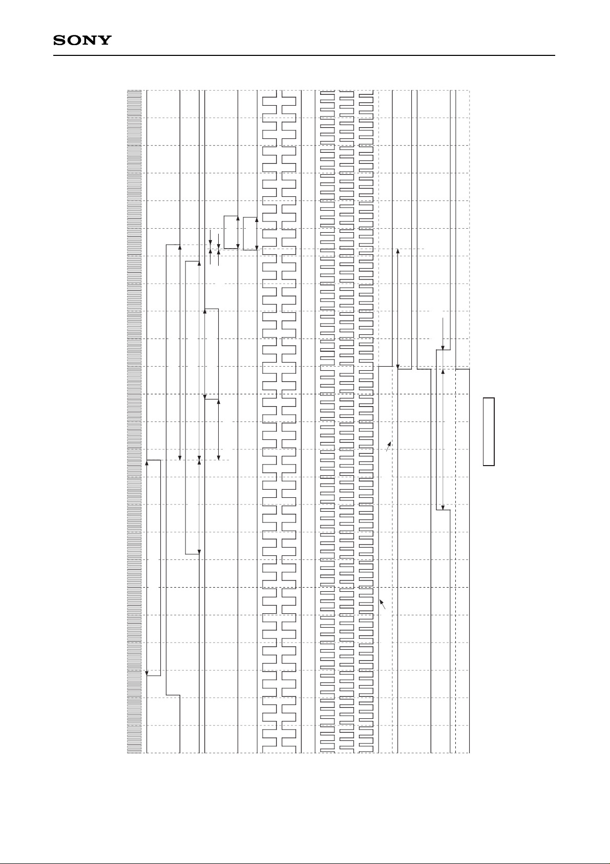
– 23 –
CXD2411AR
Note) The third row of the timing chart "BLK" is a pulse indicated as a reference and is not a pulse output from pins.
FRP polarity is not specified for each line and field.
HD
XCLP
HST1
HCK2
SH1
SH3
SH2
SH4
FRP
VCK1
HST2
CLR
MCK
XHD
HCK1
VCK2
EN
4.7µs (78fh)
4.7µs (78fh)
EVEN LINE
1.5fh
0.5fh
2.0µs (33fh)
1.3µs (22fh)
4.4µs (72fh)
2.1µs (34fh)
ODD FIELD
EVEN FIELD
0.5µs (7fh)
3.0µs (51fh)
12fh
12fh
43.5fh
HP1/2/3/4: LLLH
RGT: L (Reverse scan)
(BLK)
LCX009AK/AKB Horizontal Direction Timing Chart
NTSC/PAL
Page 24
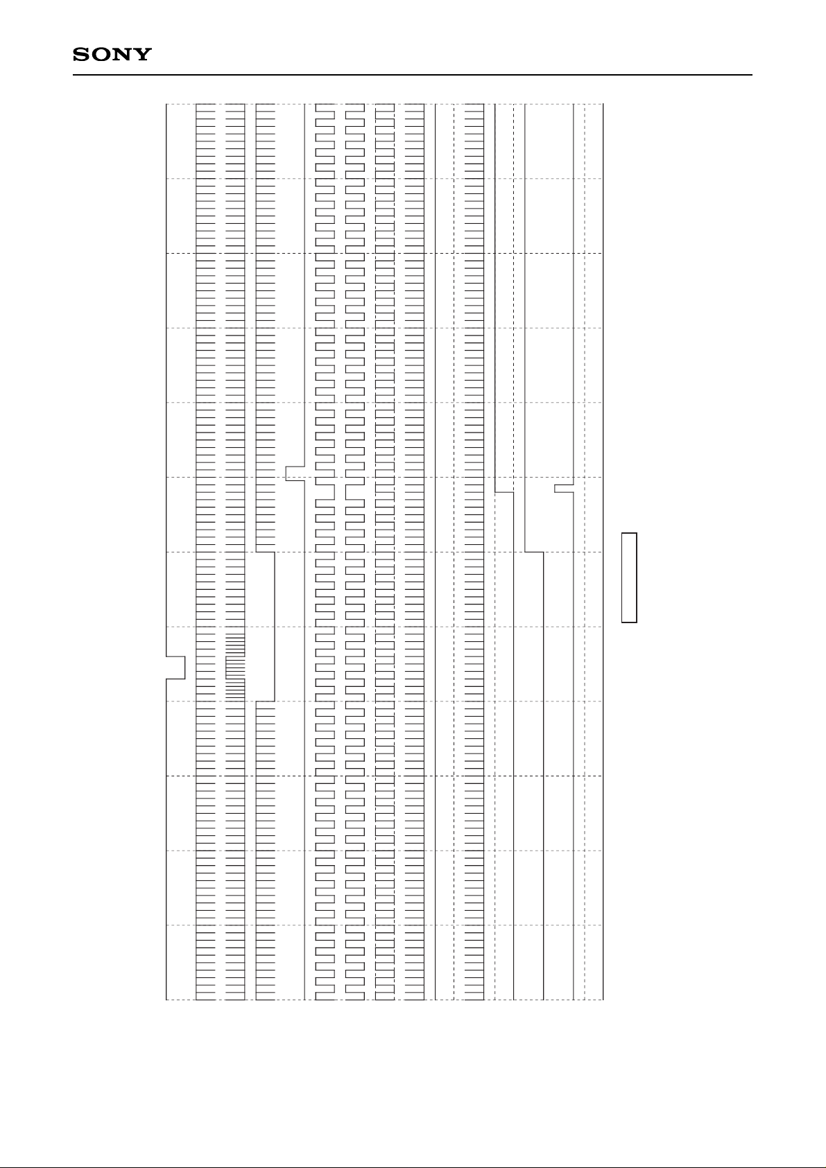
– 24 –
CXD2411AR
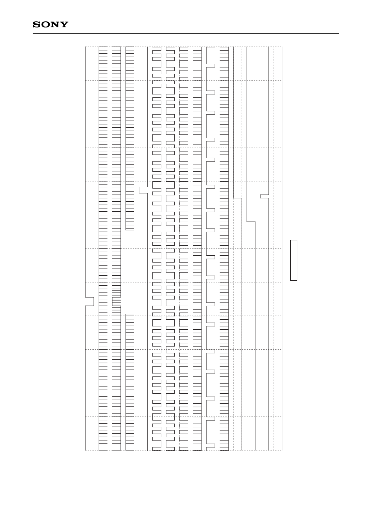
XHD
XVD
CSYNC
(BLK)
VST
VCK1
FRP
HST
CLR
EN
FRP
FLD
VD
VCK2
SBLK
ODD FIELD
Note) The fourth row of the timing chart "BLK" is a pulse indicated as a reference and is not a pulse output from pins.
FRP polarity is not specified for each line and field.
(1H inversion)
(1F inversion)
LCX005BK/BKB Vertical Direction Timing Chart
NTSC
Page 25
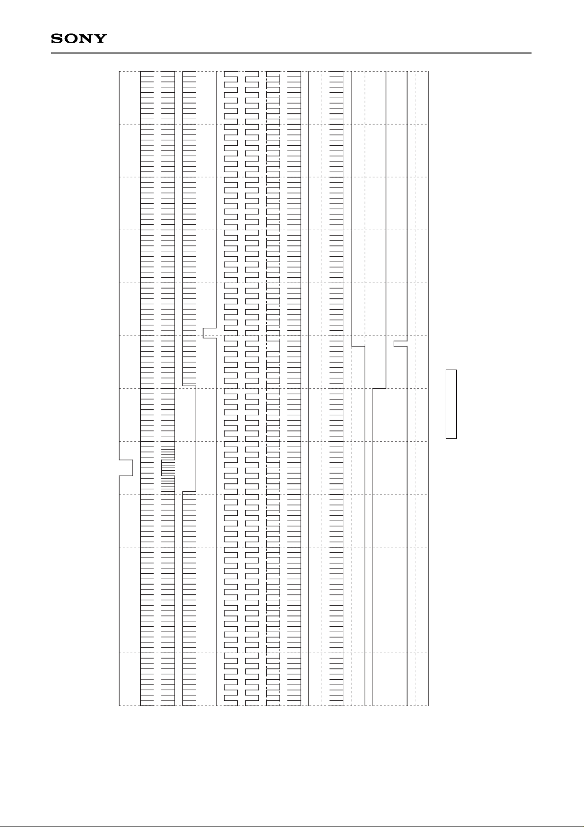
– 25 –
CXD2411AR
XHD
XVD
CSYNC
(BLK)
VST
VCK1
FRP
HST
CLR
EN
FLD
VD
VCK2
SBLK
FRP
EVEN FIELD
Note) The fourth row of the timing chart "BLK" is a pulse indicated as a reference and is not a pulse output from pins.
FRP polarity is not specified for each line and field.
(1H inversion)
(1F inversion)
LCX005BK/BKB Vertical Direction Timing Chart
NTSC
Page 26
– 26 –
CXD2411AR
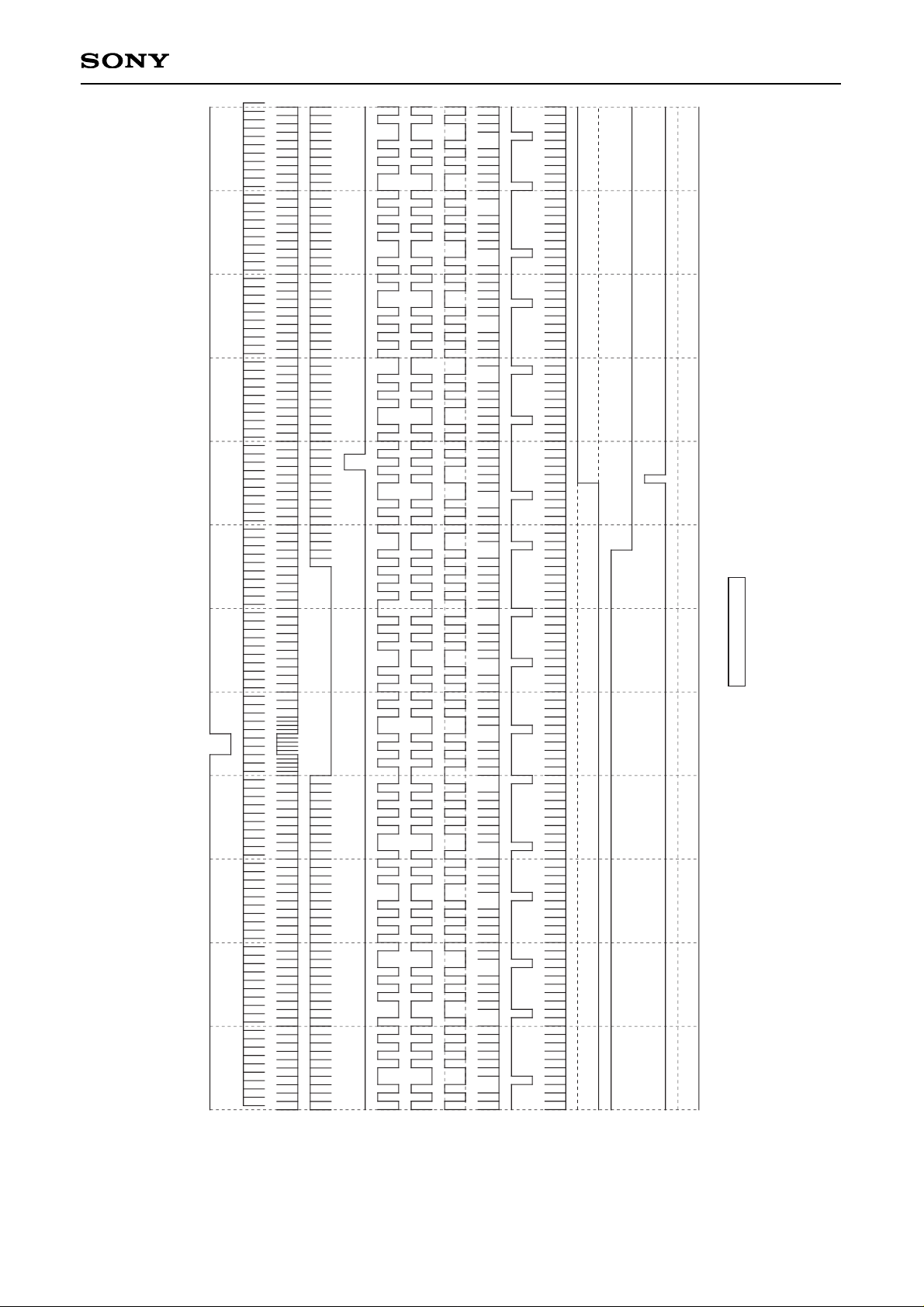
XHD
XVD
CSYNC
(BLK)
VST
VCK1
FRP
HST
CLR
EN
FLD
VD
VCK2
SBLK
FRP
ODD FIELD
Note) The fourth row of the timing chart "BLK" is a pulse indicated as a reference and is not a pulse output from pins.
FRP polarity is not specified for each line and field.
(1H inversion)
(1F inversion)
LCX005BK/BKB Vertical Direction Timing Chart
PAL
Page 27
– 27 –
CXD2411AR
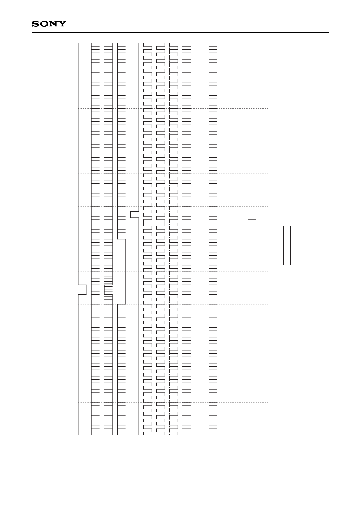
XHD
XVD
CSYNC
(BLK)
VST
VCK1
FRP
HST
CLR
EN
FLD
VD
VCK2
SBLK
FRP
EVEN FIELD
Note) The fourth row of the timing chart "BLK" is a pulse indicated as a reference and is not a pulse output from pins.
FRP polarity is not specified for each line and field.
(1H inversion)
(1F inversion)
LCX005BK/BKB Vertical Direction Timing Chart
PAL
Page 28
– 28 –
CXD2411AR
XHD
XVD
CSYNC
(BLK)
VST
VCK1
FRP
HST
CLR
EN
FRP
FLD
VD
VCK2
SBLK
ODD FIELD
Note) The fourth row of the timing chart "BLK" is a pulse indicated as a reference and is not a pulse output from pins.
FRP polarity is not specified for each line and field.
(1H inversion)
(1F inversion)
LCX009AK/AKB Vertical Direction Timing Chart
NTSC
Page 29

– 29 –
CXD2411AR
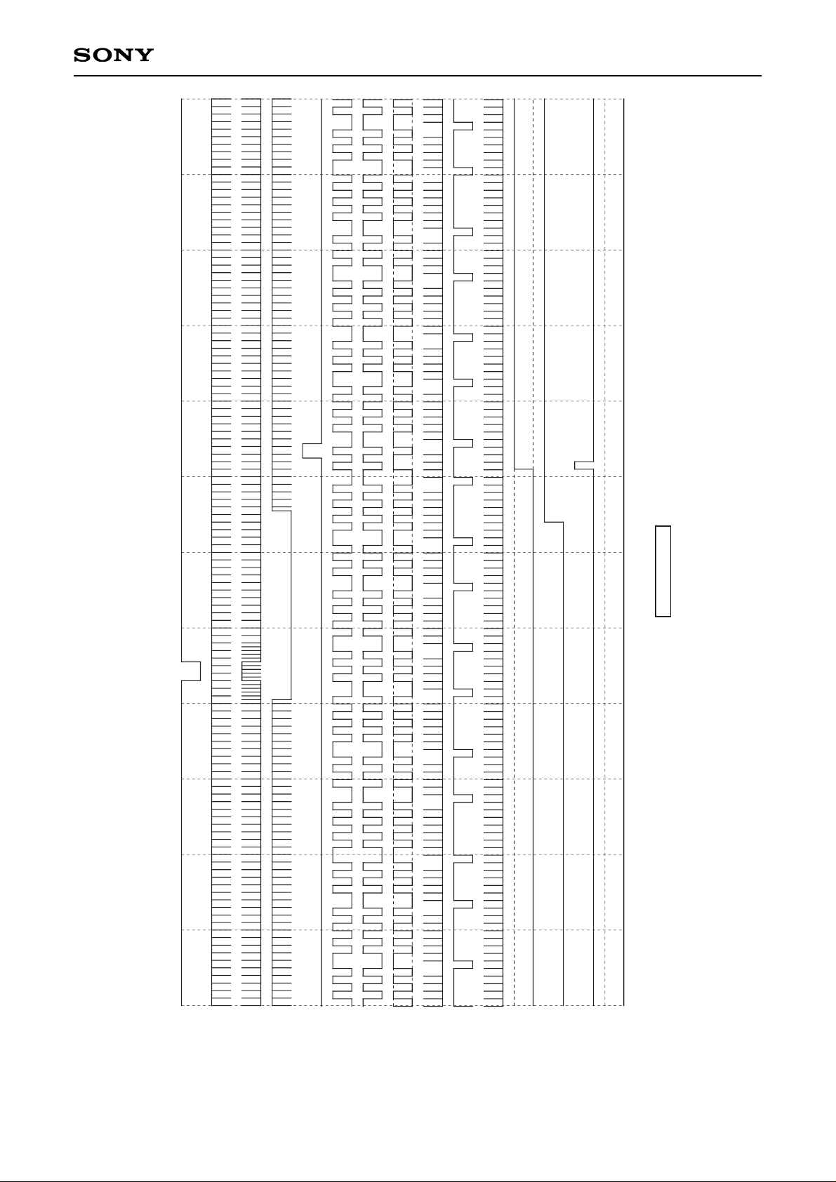
XHD
XVD
CSYNC
(BLK)
VST
VCK1
FRP
HST
CLR
EN
FLD
VD
VCK2
SBLK
FRP
EVEN FIELD
Note) The fourth row of the timing chart "BLK" is a pulse indicated as a reference and is not a pulse output from pins.
FRP polarity is not specified for each line and field.
(1H inversion)
(1F inversion)
LCX009AK/AKB Vertical Direction Timing Chart
NTSC
Page 30
– 30 –
CXD2411AR
XHD
XVD
CSYNC
(BLK)
VST
VCK1
FRP
HST
CLR
EN
FLD
VD
VCK2
SBLK
FRP
ODD FIELD
Note) The fourth row of the timing chart "BLK" is a pulse indicated as a reference and is not a pulse output from pins.
FRP polarity is not specified for each line and field.
(1H inversion)
(1F inversion)
LCX009AK/AKB Vertical Direction Timing Chart
PAL
Page 31
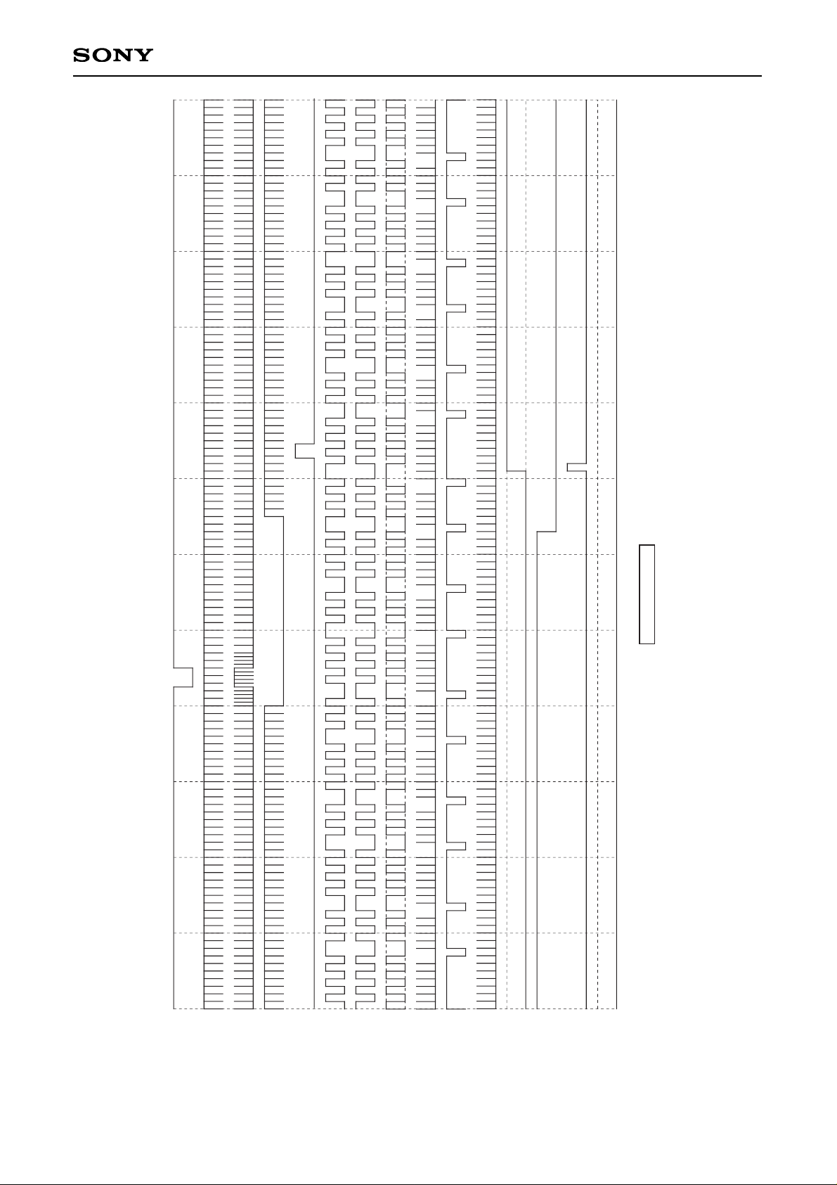
– 31 –
CXD2411AR
XHD
XVD
CSYNC
(BLK)
VST
VCK1
FRP
HST
CLR
EN
FLD
VD
VCK2
SBLK
FRP
EVEN FIELD
Note) The fourth row of the timing chart "BLK" is a pulse indicated as a reference and is not a pulse output from pins.
FRP polarity is not specified for each line and field.
(1H inversion)
(1F inversion)
LCX009AK/AKB Vertical Direction Timing Chart
PAL
Page 32

– 32 –
CXD2411AR
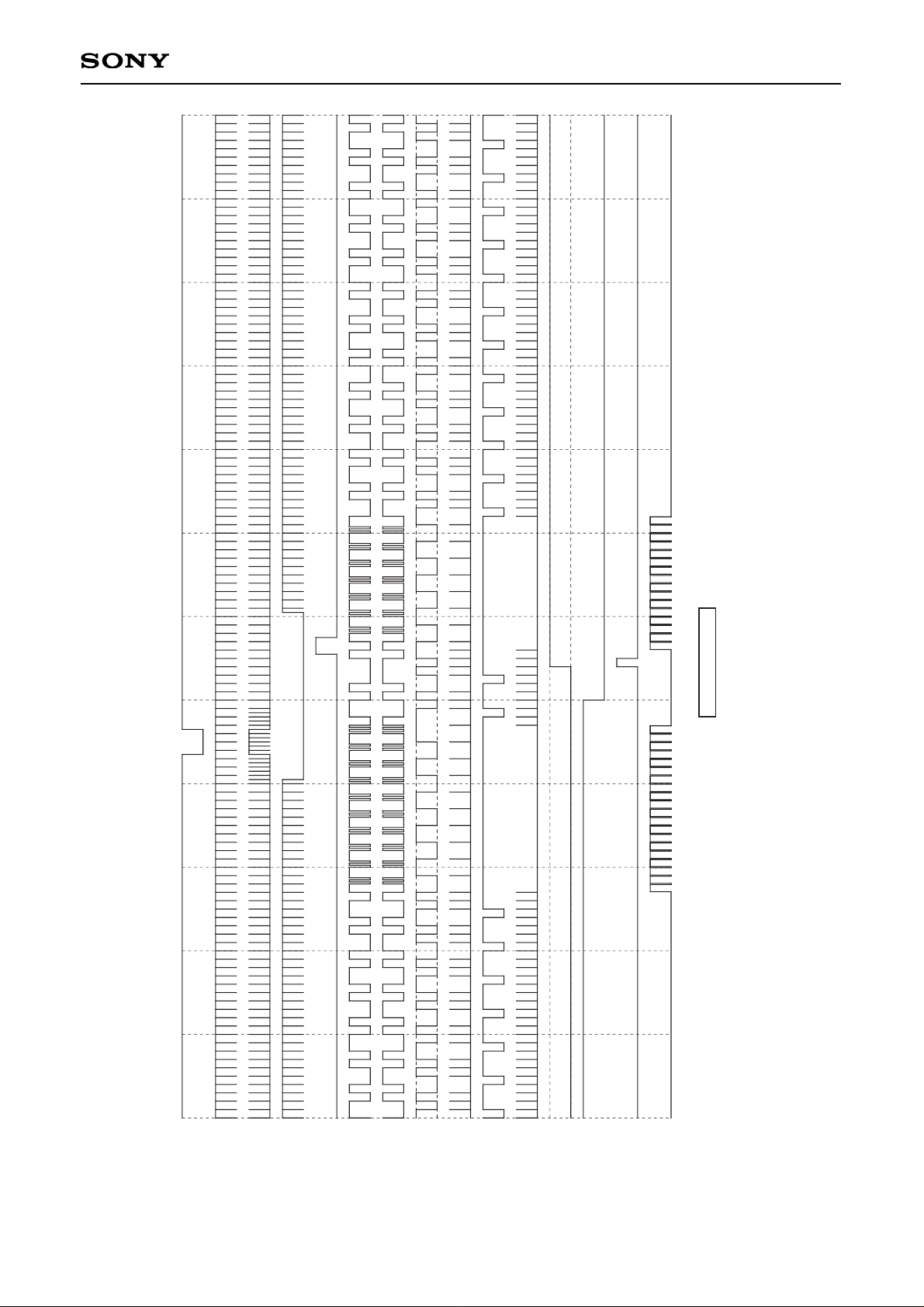
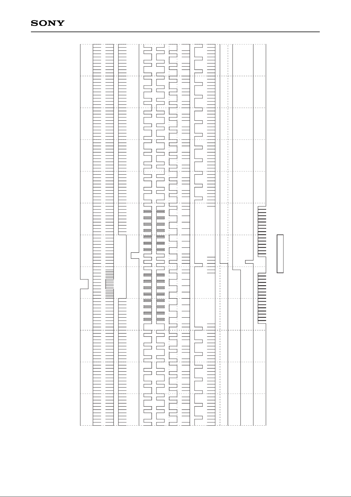
ODD FIELD
Note) The fourth row of the timing chart "BLK" is a pulse indicated as a reference and is not a pulse output from pins.
FRP polarity is not specified for each line and field.
XHD
XVD
CSYNC
(BLK)
VST
VCK1
FRP
HST
CLR
EN
FRP
FLD
VD
VCK2
SBLK
(1F inversion)
(1H inversion)
LCX005BK/BKB WIDE Vertical Direction Timing Chart
NTSC
Page 33
– 33 –
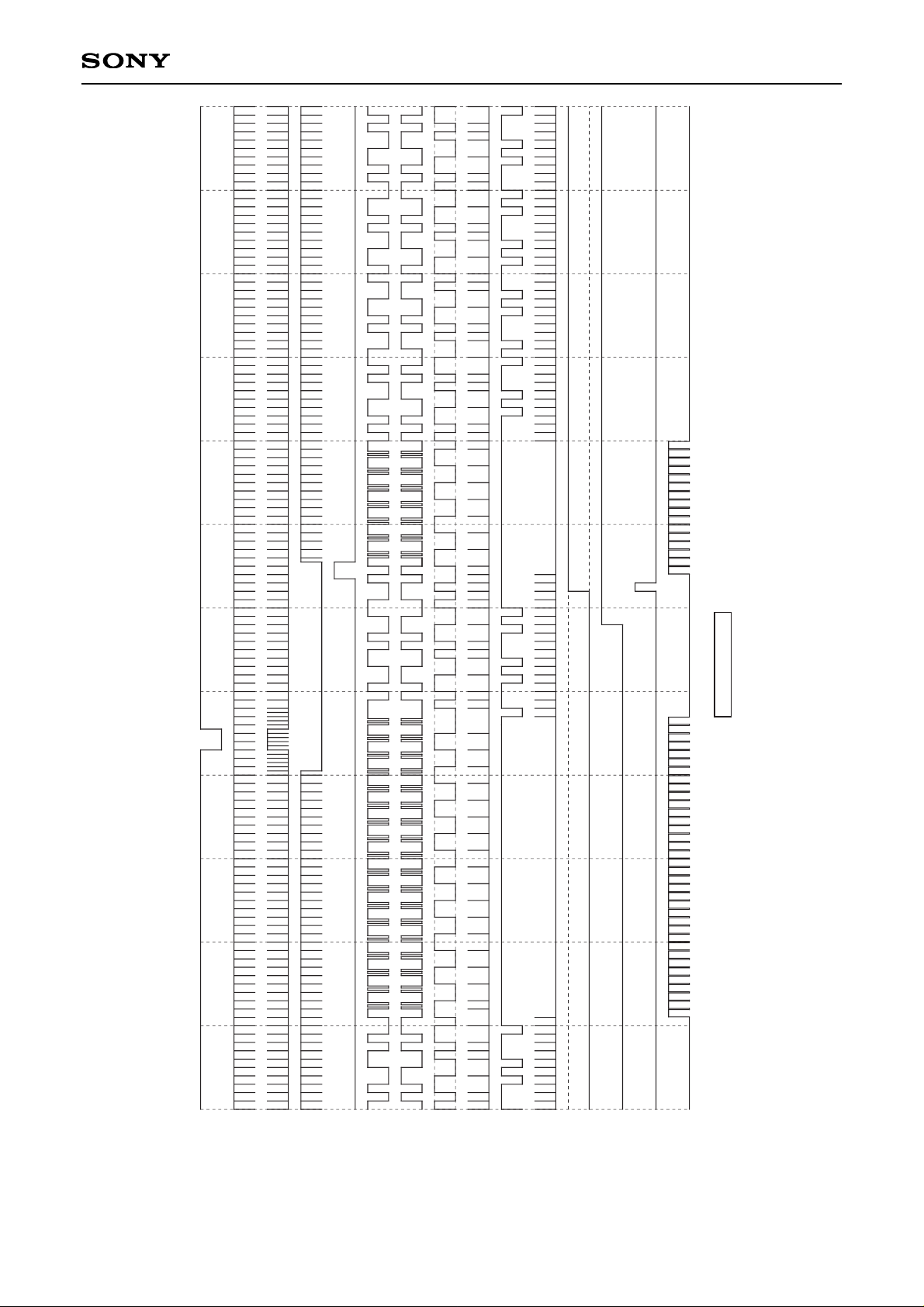
CXD2411AR
XHD
XVD
CSYNC
(BLK)
VST
VCK1
FRP
HST
CLR
EN
FLD
VD
VCK2
SBLK
FRP
EVEN FIELD
Note) The fourth row of the timing chart "BLK" is a pulse indicated as a reference and is not a pulse output from pins.
FRP polarity is not specified for each line and field.
(1H inversion)
(1F inversion)
LCX005BK/BKB WIDE Vertical Direction Timing Chart
NTSC
Page 34
– 34 –
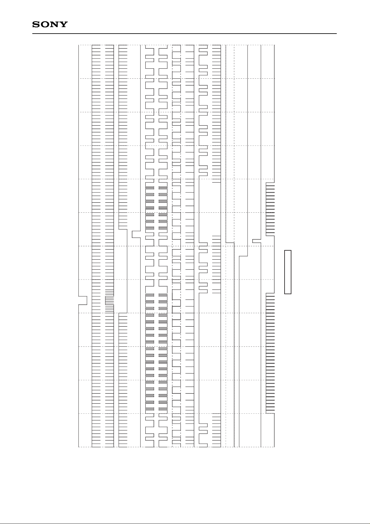
CXD2411AR
ODD FIELD
XHD
XVD
CSYNC
(BLK)
VST
VCK1
FRP
HST
CLR
EN
FLD
VD
VCK2
SBLK
FRP
Note) The fourth row of the timing chart "BLK" is a pulse indicated as a reference and is not a pulse output from pins.
FRP polarity is not specified for each line and field.
(1H inversion)
(1F inversion)
LCX005BK/BKB WIDE Vertical Direction Timing Chart
PAL
Page 35
– 35 –
CXD2411AR
XHD
XVD
CSYNC
(BLK)
VST
VCK1
FRP
HST
CLR
EN
FLD
VD
VCK2
SBLK
FRP
EVEN FIELD
Note) The fourth row of the timing chart "BLK" is a pulse indicated as a reference and is not a pulse output from pins.
FRP polarity is not specified for each line and field.
(1H inversion)
(1F inversion)
LCX005BK/BKB WIDE Vertical Direction Timing Chart
PAL
Page 36
– 36 –
CXD2411AR
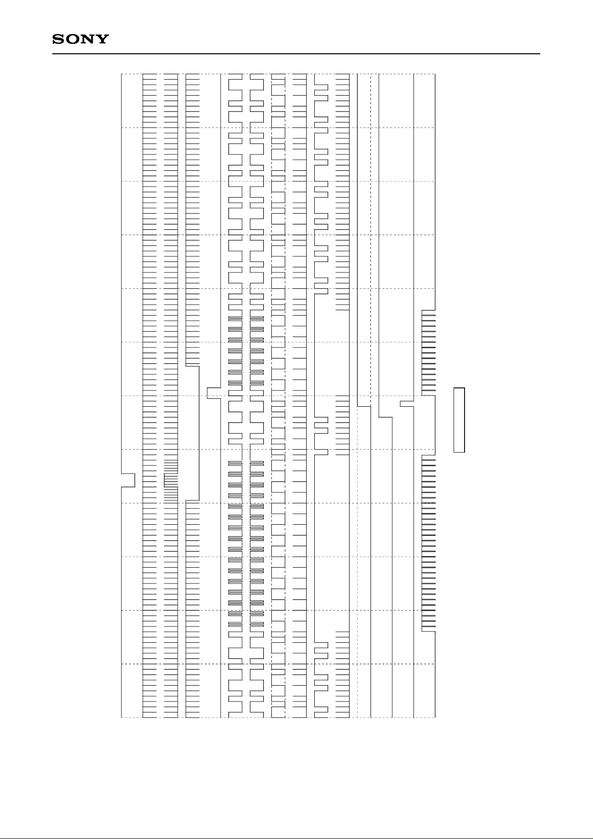
XHD
XVD
CSYNC
(BLK)
VST
VCK1
FRP
HST
CLR
EN
FRP
FLD
VD
VCK2
SBLK
ODD FIELD
Note) The fourth row of the timing chart "BLK" is a pulse indicated as a reference and is not a pulse output from pins.
FRP polarity is not specified for each line and field.
(1H inversion)
(1F inversion)
LCX009AK/AKB WIDE Vertical Direction Timing Chart
NTSC
Page 37

– 37 –
CXD2411AR
XHD
XVD
CSYNC
(BLK)
VST
VCK1
FRP
HST
CLR
EN
FLD
VD
VCK2
SBLK
FRP
EVEN FIELD
Note) The fourth row of the timing chart "BLK" is a pulse indicated as a reference and is not a pulse output from pins.
FRP polarity is not specified for each line and field.
(1H inversion)
(1F inversion)
LCX009AK/AKB WIDE Vertical Direction Timing Chart
NTSC
Page 38
– 38 –
CXD2411AR
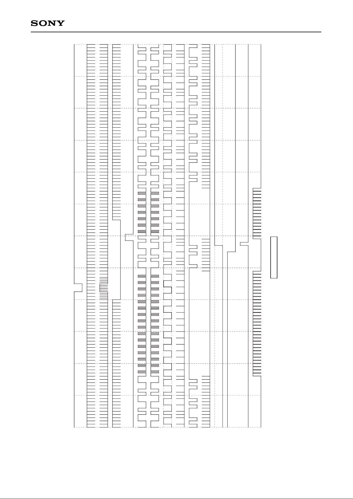
XHD
XVD
CSYNC
(BLK)
VST
VCK1
FRP
HST
CLR
EN
FLD
VD
VCK2
SBLK
FRP
ODD FIELD
Note) The fourth row of the timing chart "BLK" is a pulse indicated as a reference and is not a pulse output from pins.
FRP polarity is not specified for each line and field.
(1H inversion)
(1F inversion)
LCX009AK/AKB WIDE Vertical Direction Timing Chart
PAL
Page 39
– 39 –
CXD2411AR
XHD
XVD
CSYNC
(BLK)
VST
VCK1
FRP
HST
CLR
EN
FLD
VD
VCK2
SBLK
FRP
EVEN FIELD
Note) The fourth row of the timing chart "BLK" is a pulse indicated as a reference and is not a pulse output from pins.
FRP polarity is not specified for each line and field.
(1H inversion)
(1F inversion)
LCX009AK/AKB WIDE Vertical Direction Timing Chart
PAL
Page 40
– 40 –
CXD2411AR
AC Driving for No Signal
HST1, HST2, HCK1, HCK2, FRP, VCK1, VCK2, XCLP, HD, VD, and VST are made to run free so that the
LCD panel is AC driven even when there are no horizontal and vertical sync signals from the XHD and XVD
pins.
During this time, the PLL counter is made to run free because the horizontal sync separation circuit stops. In
addition, the auxiliary V counter is used to create the reference pulse for generating VD and VST because the
vertical sync separation circuit is also stopped.
The cycle of this V counter is designed to be 269H for NTSC and 321H for PAL. However, when there is no
vertical sync signal for 301H (NTSC) or 360H (PAL), the no signal state is assumed and the free running VD
and VST pulses are generated from the next field.
The RPD is kept at high impedance when there is no signal in order to prevent the AFC circuit from causing
phase errors due to phase comparison.
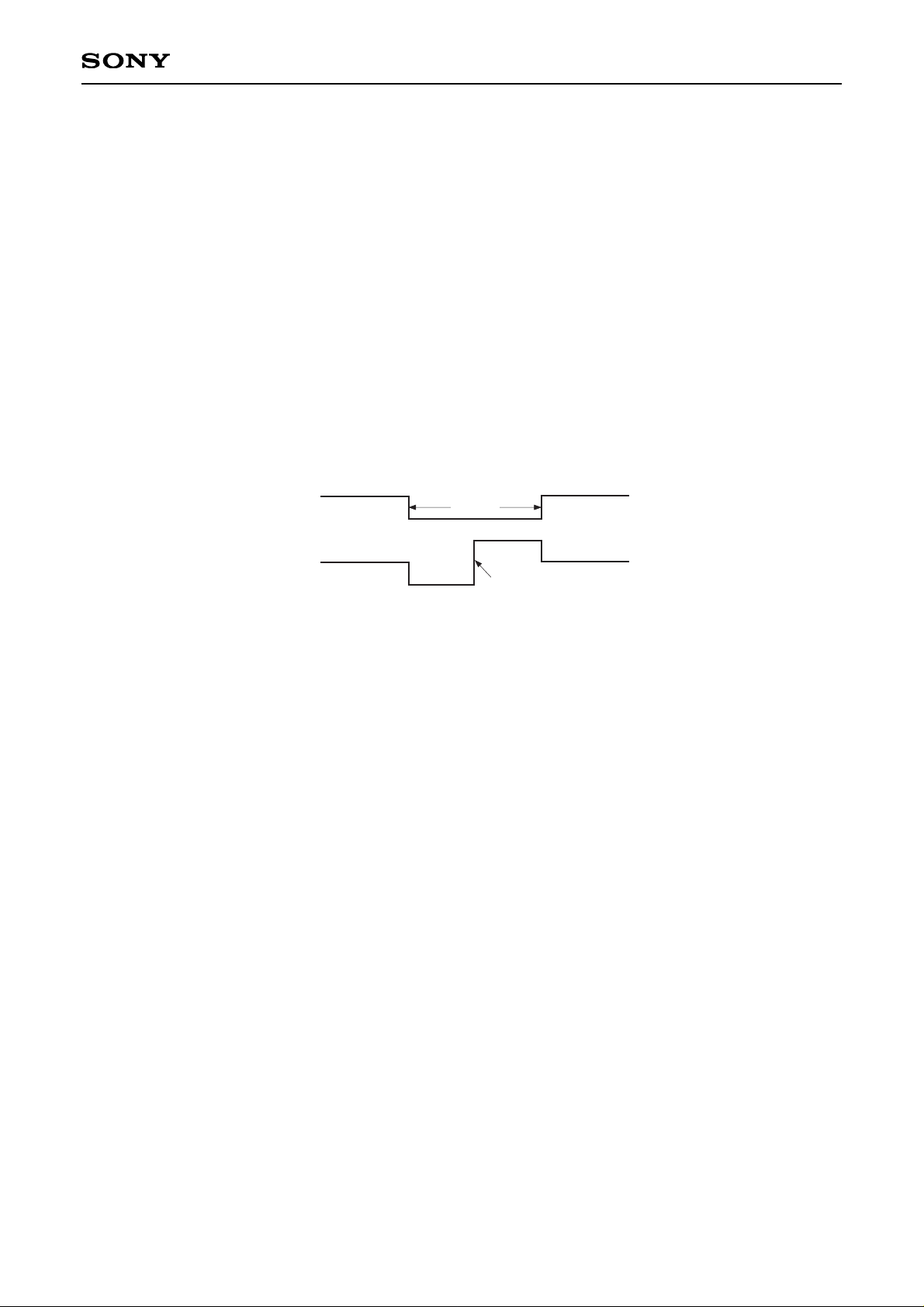
AFC Circuit (702/1050fh Generation)
The center of SYNC
4.7µs
5V
0V
RPD
2.5V
XHD
A fully synchronized AFC circuit is built in. PLL error detection signal is generated at the following timing.
The phase comparison output of the entire bottom of XHD and the internal H counter becomes RPD. RPD
output is converted to DC error with the lag-lead filter, and then it changes the varicap capacitance and the
oscillating frequency is stabilized at 702, 1050fh in the LCX005BK/BKB, LCX009AK/AKB.
Page 41

– 41 –
CXD2411AR
Application Circuit
1k
+5V
10k
3300p
33k
0.01µ
10k
100k
20p
1000p
+12V
+5V
PAL
NT
16:9
4:3
N
R
RGB external input
(RGB driver)
+5V
LCD panel
LCD panel
2
3
4
5
6
7
8
9
10
11
12
13
14
15
16
17
18
19
20
21
22
23
24
25
26
27
28
29
30
40
39
38
37
36
35
34
31
32
33
41
42
43
44
45
46
47
48
1
RGB decoder
Backlight driver circuit
RGB driver
Sample-and-hold circuit
(RGB driver)
Sample-and-hold circuit
(RGB driver)
AC conversion circuit (RGB driver)
HCK1
3.3µ
LCX005BK/BKB
LCX009AK/AKB
L
RGB decoder
HD
XHD
N.C.
VD
XCLP
SH3
SH2
SH1
V
SS
SH4
FLDO
FRP
HCK2
HST1
VCK1
VCK2
V
DD
VST
EN
CLR
N.C.
HST2
SLFR
SLCK
RGT
N.C.
N.C.
PLNT
XCLR
WIDE
SBLK
V
SS
TST0
TST1
TST2
N.C.
HP4
RPD
V
SS
CKO
CKI
V
DD
N.C.
XVD
FP1
FP2
FP3
Reference examples of L value: when using LCX009AK/AKB 4.7µH Recommended varicap: 1T369 (SONY)
when using LCX005BK/BKB 10µH
Application circuits shown are typical examples illustrating the operation of the devices. Sony cannot assume responsibility for
any problems arising out of the use of these circuits or for any infringement of third party patent and other right due to same.
Page 42
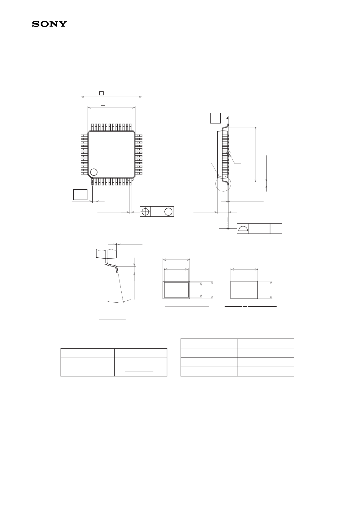
– 42 –
CXD2411AR
Package Outline Unit: mm
SONY CODE
EIAJ CODE
JEDEC CODE
PACKAGE MATERIAL
LEAD TREATMENT
LEAD MATERIAL
PACKAGE MASS
EPOXY RESIN
PLATING
42/COPPER ALLOY
PACKAGE STRUCTURE
48PIN LQFP (PLASTIC)
9.0 ± 0.2
∗ 7.0 ± 0.1
1
12
13
24
25
36
37
48
(0.22)
0.18 – 0.03
+ 0.08
0.2g
LQFP-48P-L01
LQFP048-P-0707
(8.0)
0.5 ± 0.2
0.127 – 0.02
+ 0.05
A
1.5 – 0.1
+ 0.2
0.1
SOLDER/PALLADIUM
NOTE: Dimension “∗” does not include mold protrusion.
0.1 ± 0.1
0.5 ± 0.2
0° to 10°
DETAIL A
0.13
M
0.5
S
S
B
DETAIL B:SOLDER
(0.18)
(0.127)
DETAIL B:PALLADIUM
0.127 ± 0.04
0.18 – 0.03
+ 0.08
0.127 – 0.02
+0.05
0.18 ± 0.03
 Loading...