

Page 1

Timing Controller for ICX076/077AL
Description
The CXD2409R is a timing controller for CCD
camera systems which use the ICX076/077AL
black-and-white CCD image sensors.
Features
• Supports EIA/CCIR standards
• Electronic iris (electronic shutter) function
• Sync signal generation function
• Backlight compensation function
• AGC flickerless circuit
• Electronic iris power on reset function
• Oscillator frequency: 13.5 MHz
CXD2409R
64 pin LQFP (Plastic)
Applications
• Doorphones
• Small sized surveillance cameras
Absolute Maximum Ratings (Ta = 25°C)
• Supply voltage VDD VSS – 0.5 to +7.0 V
• Input voltage VI
• Output voltage VO
•
Operating temperature
•
Storage temperature
Recommended Operating Conditions
• Supply voltage VDD 5.0 ± 0.25 V
•
Operating temperature
CCD Image Sensors Used
ICX076/077AL
VSS – 0.5 to VDD + 0.5
VSS – 0.5 to VDD + 0.5
Topr –20 to +75 °C
Tstg –55 to +150 °C
Topr –20 to +75 °C
Structure
Silicon gate CMOS IC
V
V
Sony reserves the right to change products and specifications without prior notice. This information does not convey any license by
any implication or otherwise under any patents or other right. Application circuits shown, if any, are typical examples illustrating the
operation of the devices. Sony cannot assume responsibility for any problems arising out of the use of these circuits.
– 1 –
E94847A52-PP
Page 2

CXD2409R
1
1
SS
DD
SS
DD
SV
33
SV
27
WSEL2
60
WSEL1
59
CLP2
43
CLP1
44
XV4
XV3
13
XV2
10
XV1
11
XSG2
14 15
XSG1
12
SHD
39
SHP
38
RG
7
H2
5
H1
4
AV
6
AV
3
VD
49
HD
50
CL
48
OSCO
1
OSCI
2
WND
42
DETC3
AGCO2
32
34
CKI
DETC2
31
FL
64
DETC1
30
1/2
AGCI2
29
TG
56
DD
V
AGCO1
28
1/429
1/432
9
VDD
WND
55
VSS
AGCI1
26
8
VSS
PS
51
1/525
IRIN/ED1
20
SSG
1/625
DETC4
18
WND
DECODE
IRIS
/SHUTTER
45
SYNC
Vreg
21
CLK GEN.
46
47
FLD
CBLK
SPUPV/ED0
24
COMP
ADDER
UP/DOWN
COUNT LIMIT SELECT
GATE
TEST
35
36
TEST1
TEST2
SPDNV/ED2
23
COMP
41
TEST3
19
17
25
22
37
40
52
61
63
62
54
53
16
57
58
SS
2
SV
SV
DD
2
CV
SS
CV
DD
V
SS
V
SS
IRENB
LLIM
HLIM2
HLIM1
POWER
ENB
XSUB
FL
EIA
Block Diagram
X'tal
13.5MHz
– 2 –
Page 3

Pin Configuration (Top View)
48
49
VD
50
HD
51
PS
52
IRENB
53
ENB
V
VDD
FL
EIA
LLIM
CKI
SS
54
55
56
57
58
59
60
61
62
63
64
POWER
WSEL1
WSEL2
HLIM1
HLIM2
CL
47
FLD
46
CBLK
45
SYNC
44
CLP1
43
CLP2
42
WND
41
SS
TEST3
V
40
39
SHD
38
SHP
37
SS
V
TEST2
36
TEST1
35
AGCO2
34
33
1
SS
SV
32
DETC3
31
DETC2
30
DETC1
29
AGCI2
28
AGCO1
27
SV
26
AGCI1
25
CV
24
SPUPV/ED0
23
SPDNV/ED2
22
CV
21
Vreg
IRIN/ED1
20
19
SV
18
DETC4
17
SVDD2
CXD2409R
DD1
SS
DD
SS2
Pin Description
Pin
No.
1
2
3
4
5
6
7
8
9
10
11
Symbol I/O Description
OSCO
OSCI
AVDD
H1
H2
AVSS
RG
VSS
VDD
XV2
XV1
6
DD
AV
5
4
H1
H2
7
SS
AV
1
2
3
OSCI
OSCO
O
Oscillation inverter output
I
Oscillation inverter input
—
Power supply (for H1, H2)
O
Clock output for CCD horizontal register drive
O
Clock output for CCD horizontal register drive
—
GND (for H1, H2)
O
Reset gate pulse output
—
GND
—
Power supply
O
Clock output for CCD vertical register drive
O
Clock output for CCD vertical register drive
RG
9
SS
V
DD
V
10
8
XV2
11
XV1
12
13
XSG1
14 15
XV3
XSG2
XV4
16
XSUB
12
XSG1
O
CCD sensor charge readout pulse output
– 3 –
Page 4

CXD2409R
Pin
No.
13
14
15
16
17
18
19
20
21
22
23
24
25
26
27
28
29
30
31
32
Symbol I/O Description
O
XV3
XSG2
XV4
XSUB
SVDD2
DETC4
SVSS2
IRIN/ED1
Vreg
CVDD
SPDNV/ED2
SPUPV/ED0
CVSS
AGCI1
SVDD1
AGCO1
AGCI2
DETC1
DETC2
DETC3
Clock output for CCD vertical register drive
O
CCD sensor charge readout pulse output
O
Clock output for CCD vertical register drive
O
CCD discharge pulse output
—
Power supply (for the iris window switch)
O
Capacitor for iris detection
—
GND (for the iris window switch)
I
Iris signal input/shutter speed setting; clock input in serial mode
I
Bias current supply for the comparator
—
Power supply (for the comparator)
Shutter speed down reference voltage/
I
shutter speed setting; data input in serial mode
Shutter speed up reference voltage/
I
shutter speed setting; strobe input in serial mode
—
GND (for the comparator)
I
AGC detection signal input
—
Power supply (for the AGC window switch)
O
AGC detection signal output
I
AGC flickerless circuit input
O
AGC detection capacitor 1
O
AGC detection capacitor 2
O
AGC detection capacitor 3
33
34
35
36
37
38
39
40
41
42
43
44
45
46
47
SVSS1
AGCO2
TEST1
TEST2
VSS
SHP
SHD
VSS
TEST3
WND
CLP2
CLP1
SYNC
CBLK
FLD
—
GND (for the AGC window switch)
O
AGC flickerless circuit output
I
Test input (with the pull-down resistor)
I
Test input (with the pull-down resistor)
—
GND
O
Precharge level sample-and-hold pulse
O
Data sample-and-hold pulse
—
GND
I
Test input (with the pull-down resistor)
O
Window pulse output
O
Pulse output for clamp
O
Pulse output for clamp
O
Composite sync output
O
Composite blanking output
O
Field pulse output
– 4 –
Page 5

CXD2409R
Pin
No.
48
49
50
51
52
53
54
55
56
57
58
59
60
61
Symbol I/O Description
O
CL
VD
HD
PS
IRENB
ENB
POWER
VSS
VDD
FL
EIA
WSEL1
WSEL2
LLIM
Master clock output
O
Vertical sync signal output
O
Horizontal sync signal output
Electronic shutter speed input switchover
I
Low: serial input; high: parallel input (with the pull-up resistor)
I
Low:
electronic shutter mode; high: electronic iris mode (with the pull-up resistor
I
Low: XSUB pulse stop; high: XSUB pulse output (with the pull-up resistor)
I
Electronic iris power on reset
—
GND
—
Power supply
I
Low: normal mode; high:AGC flickerless mode (with the pull-down resistor)
I
Low: EIA; high: CCIR (with the pull-down resistor)
I
Window pulse output switchover (with the pull-down resistor)
I
Window pulse output switchover (with the pull-down resistor)
Electronic iris low speed limiter switchover
I
Low: limiter OFF; high: limiter ON (with the pull-down resistor)
)
62
63
64
HLIM1
HLIM2
CKI
I
Electronic iris high speed limiter switchover (with the pull-down resistor)
I
Electronic iris high speed limiter switchover (with the pull-down resistor)
I
2 fck clock input
– 5 –
Page 6
CXD2409R
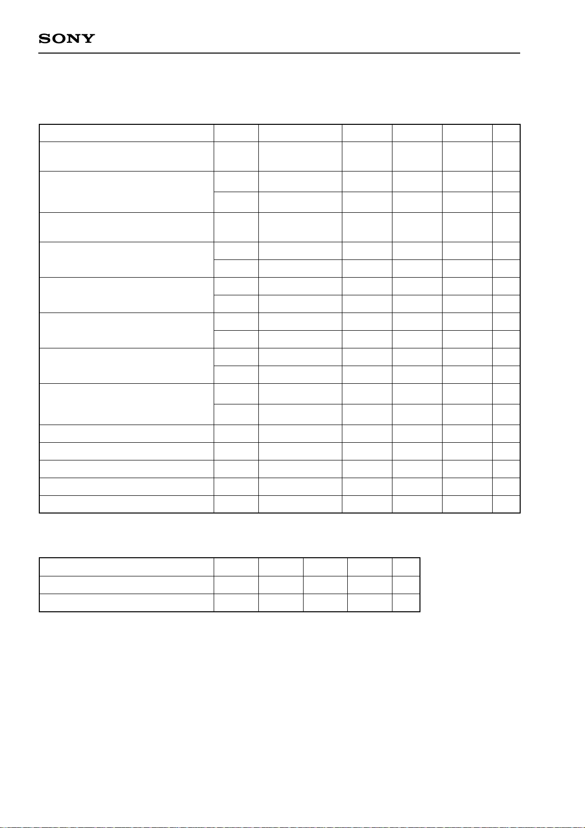
Electrical Characteristics
DC Characteristics (VDD = 4.75 to 5.25V, Topr = –20 to +75°C)
Item
Supply voltage
Pins 3, 9, 17, 22, 27, and 56
Input voltage 1
All input pins except Pins 20, 21, 23,
24, 26, and 29
Input voltage 2
Pins 20, 21, 23, 24, 26, and 29
Output voltage 1
Pins 4, 5, and 7
Output voltage 2
Pins 38 and 39
Output voltage 3
Pins 18, 28, 30, 31, 32, and 34
Output voltage 4
Pin 48
Output voltage 5
Pins 10, 11, 12, 13, 14, 15, 16, 42, 43,
44, 45, 46, 47, 49, and 50
Symbol Conditions Min. Typ. Max. Unit
VDD
VIH
VIL
VIN
VOH1
VOL1
VOH2
VOL2
VOH3
VOL3
VOH4
VOL4
VOH5
VOL5
IOH = –7mA
IOL = 20mA
IOH = –4mA
IOL = 8mA
IOH = –4mA
IOL = 8mA
IOH = –2mA
IOL = 4mA
4.75
0.7VDD
1.9
VDD – 0.8
VDD – 0.8
VDD – 0.8
VDD – 0.8
5.0
5.25
0.3VDD
5.0
0.4
0.4
0.4
0.4
V
V
V
V
V
V
V
V
V
V
V
V
V
V
Feedback resistance
Pull-up resistance
Pull-down resistance
Analog switch ON resistance
Current consumption
RFB
RPU
RPD
RON
IDD
VIN = VSS or VDD
VIN = 2.5V ± 1V
250k
20k
20k
20k
1M
50k
50k
50k
Input/Output Capacitance (VDD = VSS = 0V, VI or VO = 0V, fM = 1MHz)
Item
Input pin capacitance
Output pin capacitance
Symbol Min. Typ. Max. Unit
CIN
COUT
11
9
pF
pF
2.5M
125k
125k
200
125k
Ω
Ω
Ω
Ω
mA
– 6 –
Page 7

Mode Control
Pin
No.
Symbol I/O Low High Remarks
CXD2409R
52
53
58
59
60
61
62
63
57
51
IRENB
ENB
EIA
WSEL1
WSEL2
LLIM
HLIM1
HLIM2
FL
PS
I
I
I
I
I
I
I
I
I
I
Electronic shutter
XSUB stop
EIA
Four types of window settings can be selected by
combining WSEL1 and WSEL2.
The minimum shutter speed can be selected during
electronic iris mode.
The maximum shutter speed can be selected during
electronic iris mode by combining HLIM1 and HLIM2.
AGC flickerless OFF
Serial input
Electronic iris
XSUB output
CCIR
AGC flickerless ON
Parallel input
Valid when ENB is high.
Valid when ENB is high
and IRENB is high.
Valid when ENB is high
and IRENB is high.
Valid when AGC is used.
Valid when ENB is high
and IRENB is low.
• The functions of the pins (Pins 20, 23, and 24) listed below change according to the IRENB (Pin 52) mode
setting.
(Valid when ENB is high.)
Pin
No.
20
23
24
Symbol I/O
IRIN
/ED1
SPDNV
/ED2
SPUPV
/ED0
I
I
I
Low High
Electronic shutter speed setting;
clock input in serial mode
Electronic shutter speed setting;
data input in serial mode
Electronic shutter speed setting;
strobe input in serial mode
IRENB
IRIS signal input
Comparator reference voltage input
(shutter speed down side)
Comparator reference voltage input
(shutter speed up side)
– 7 –
Page 8

CXD2409R
Description of Operation
Electronic Shutter/Electronic Iris
By setting the ENB pin (Pin 53) high, the XSUB pulse is output for a specific period to activate the electronic
shutter and electronic iris.
Electronic Shutter
Parallel input (IRENB = low, PS = high)
Mode
OFF
Electronic
shutter
EIA
CCIR
EIA
CCIR
EIA ENB IRENB SPUPV IRIN SPDNV Shutter speed
L
H
L
L
L
L
L
L
L
L
H
H
H
H
H
H
H
H
L
L
H
H
H
H
H
H
H
H
H
H
H
H
H
H
H
H
×
×
L
L
L
L
L
L
L
L
L
L
L
L
L
L
L
L
×
×
H
L
H
L
H
L
H
L
H
L
H
L
H
L
H
L
×
×
H
H
L
L
H
H
L
L
H
H
L
L
H
H
L
L
×
×
H
H
H
H
L
L
L
L
H
H
H
H
L
L
L
L
1/60 (s)
1/50 (s)
1/100 (s)
1/250 (s)
1/500 (s)
1/1000 (s)
1/2000 (s)
1/5000 (s)
1/10000 (s)
1/100000 (s)
1/120 (s)
1/250 (s)
1/500 (s)
1/1000 (s)
1/2000 (s)
1/5000 (s)
1/10000 (s)
1/70000 (s)
– 8 –
Page 9
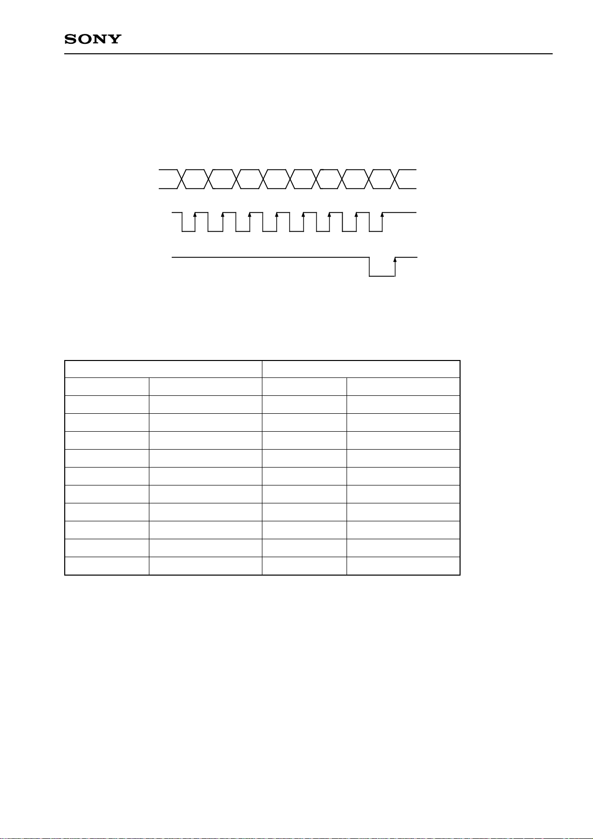
Serial input (IRENB = low, PS = low)
By inputting 8-bit data to the ED2 pin (Pin 23), the electronic shutter speed can be controlled.
Serial input data format
CXD2409R
SPDNV/ED2
IRIN/ED1
SPUPV/ED0
D6D7
D4D5
D3
D2
D1
D0
The ED2 (Pin 23) data is latched in the register at the ED1 (Pin 20) rise, and retrieved internally at the ED0
(Pin 24) rise.
Typical shutter speeds
Shutter speed (s)
1/60
1/100
1/250
1/500
EIA
DATA (ED0: 8bit)
11111111 (0 step)
11110110 (9 step)
11100101 (26 step)
11010010 (45 step)
Shutter speed (s)
1/50
1/120
1/250
1/500
CCIR
DATA (ED0: 8bit)
11111111 (0 step)
11110001 (14 step)
11100011 (28 step)
11010000 (47 step)
1/1000
1/2000
1/5000
1/10000
1/30000
1/100000
11000010 (61 step)
10111000 (71 step)
10101000 (87 step)
10011011 (100 step)
10000010 (125 step)
01101010 (149 step)
1/1000
1/2000
1/5000
1/10000
1/30000
1/100000
11000000 (63 step)
10110111 (72 step)
10100110 (89 step)
10011000 (103 step)
01111101 (130 step)
01100011 (156 step)
– 9 –
Page 10
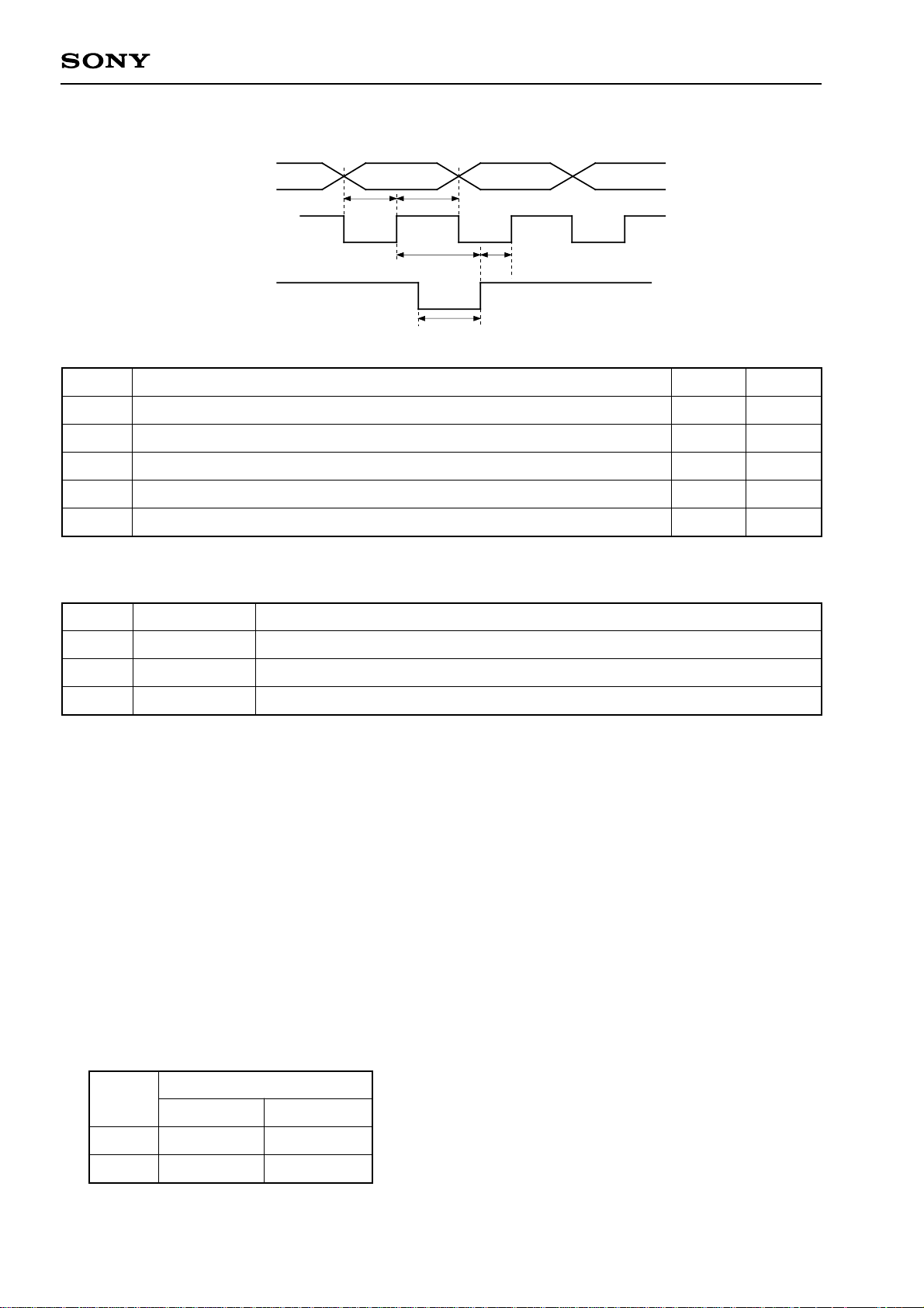
AC Characteristics
SPDNV/ED2
CXD2409R
Symbol
ts2
th2
ts1
tw0
ws0
SPDNV (ED2) setup time for IRIN (ED1) rise
SPDNV (ED2) hold time for IRIN (ED1) rise
IRIN (ED1) setup time for SPUPV (ED0) rise
SPUPV (ED0) pulse width
SPUPV (ED0) setup time for IRIN (ED1) rise
Electronic Iris
Pin No.
20
IRIN/ED1
ts2
IRIN/ED1
SPUPV/ED0
th2
ts1
ts0
tw0
Symbol Function
Iris signal input
Min. Max.
20ns
20ns
20ns
20ns
20ns
—
—
—
50µs
—
(ENB = high, IRENB = high)
23
24
SPDNV/ED2
SPUPV/ED0
Comparator reference voltage input for shutter speed down
Comparator reference voltage input for shutter speed up
(a) Electronic iris characteristics
Shutter speed : 1/60 to 1/100000 (s) (EIA)
1/50 to 1/70000 (s) (CCIR)
Iris steps : 149 steps (EIA)
151 steps (CCIR)
Contraction ratio for one iris step : average 6%
Note) When LLIM = low, HLIM1 = low, and HLIM2 = low
(b) LLIM (low speed shutter limiter)
By setting the LLIM pin (Pin 61) high, the minimum shutter speed can be changed.
(ENB = high, IRENB = high)
Minimum shutter speed
LLIM
EIA CCIR
L
H
1/60
1/100
1/50
1/120
– 10 –
Page 11
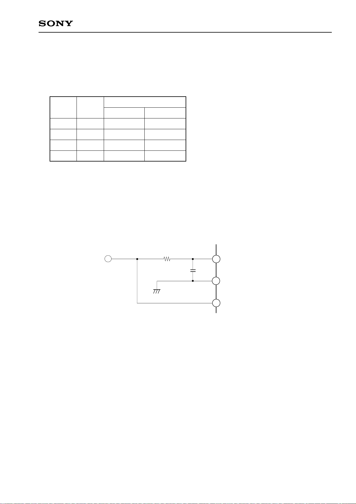
(c) HLIM (high speed shutter limiter)
By combining the HLIM1 pin (Pin 62) and the HLIM2 pin (Pin 63), the maximum shutter speed can be
changed.
(ENB = high, IRENB = high)
CXD2409R
HLIM1
HLIM2
EIA CCIR
Maximum shutter speed
L
H
H
L
L
L
H
H
1/100000 (s)
1/30000 (s)
1/10000 (s)
1/5000 (s)
1/70000 (s)
1/30000 (s)
1/10000 (s)
1/5000 (s)
(d) Power on reset
During electronic iris mode (IRENB = high), the initial settings for the iris are made in the instant the
POWER pin (Pin 54) switches from low to high.
The initial setting shutter speed is 1/1000 (s).
By applying the circuit shown below, the shutter speed can be initialized when the power is turned on.
+5 V power supply
100k
0.68µ
54
POWER
55
56
V
SS
V
DD
– 11 –
Page 12
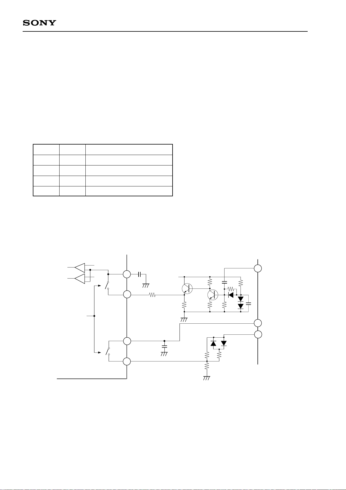
(e) Backlight compensation
By applying the window pulse to the electronic iris detection signal (IRIS) input to IRIN (Pin 20) and the
AGC detection signal (DET OUT) input to AGCI1 (Pin 26), backlight compensation can be performed.
Compensation is achieved by detecting a limited area with the built-in analog switch for the window and the
external sample-and-hold capacitor. In addition, four types of backlight compensation areas can be
selected by combining the WSEL1 pin (Pin 59) and WSEL2 pin (Pin 60) as shown in the table below.
The basic circuit to perform the window operations is shown in the figure below, and window pulse timing
charts are shown on the following pages.
Window types
CXD2409R
WSEL1
L
H
L
H
∗1
The signal is masked during blanking.
WSEL2
L
L
H
H
Minimum shutter speed
Full measurement
Lower measurement
Center measurement
Lower center measurement
Basic Circuit Configuration
Comparator for iris
Iris window switch
Window pulse
(WND)
CXD2409R
AGC window switch
DETC4
IRIN
AGCO1
AGCI1
18
20
28
26
∗1
GND
2SC2785
10k
GND
+5V
39k
2SC2785
10k 10k
10k
100k
1µ
1k
10k
10k
27
19
13
IRIS
CXA1310Q
OP+
DET OUT
– 12 –
Page 13
CXD2409R
XSG1
EIA
V direction timing
XV1
WND
11 XV1
249 XV1
CL
XV1
H direction timing
6.75MHz
WND
40 CL
394 CL
XSG1
CCIR
V direction timing
XV1
WND
10 XV1
294 XV1
XV1
CL
H direction timing
6.75MHz
WND
45 CL
395 CL
1. Full measurement
Window Pulse Response Chart
WSEL1 = L / WSEL2 = L
– 13 –
Page 14

CXD2409R
A
A
XSG1
EIA
V direction timing
XV1
WND
249 XV1
189 XV1
XV1
CL
H direction timing
WND
6.75MHz
40 CL
394 CL
XSG1
CCIR
V direction timing
XV1
WND
223 XV1
294 XV1
XV1
CL
H direction timing
WND
6.75MHz
45 CL
395 CL
WSEL1 = H / WSEL2 = L
2. Lower measurement
AAAA
AAAA
– 14 –
Page 15

CXD2409R
A
A
A
XSG1
EIA
V direction timing
XV1
WND
70 XV1
189 V1
XV1
6.75MHz
WND
CL
H direction timing
158 CL
276 CL
XSG1
CCIR
V direction timing
XV1
WND
223 XV1
152 XV1
XV1
CL
H direction timing
WND
6.75MHz
288 CL
170 CL
WSEL1 = L / WSEL2 = H
3. Center measurement
AAAAA
AAAAA
AAAAA
– 15 –
Page 16
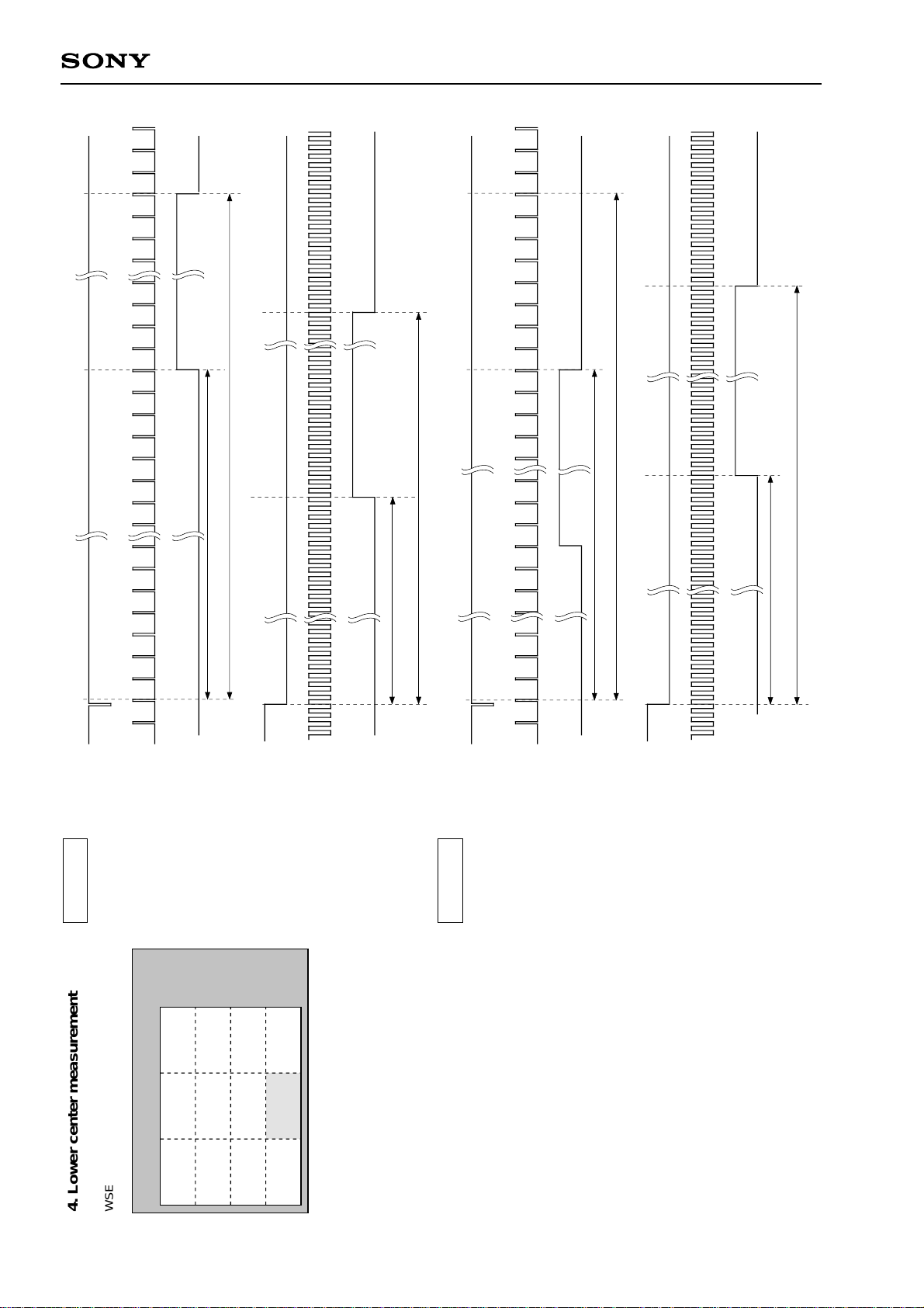
CXD2409R
A
A
A
XSG1
EIA
V direction timing
XV1
WND
189 XV1
249 XV1
XV1
CL
H direction timing
6.75MHz
WND
158 CL
276 CL
XSG1
CCIR
V direction timing
XV1
WND
294 XV1
223 XV1
XV1
CL
H direction timing
6.75MHz
WND
288 CL
170 CL
AAAA
4. Lower center measurement
WSEL1 = H / WSEL2 = H
AAAA
AAAA
– 16 –
Page 17
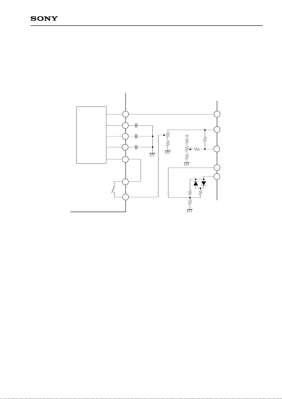
CXD2409R
AGC Flickerless
By setting the FL pin (Pin 57) of the CXD2409R high when using the CXA1310Q AGC, the fluorescent light
flicker component generated by differences between the fluorescent light emission cycle and the EIA field
cycle can be controlled.
Basic Circuit Configuration
AGCO2
CXD2409R
Flickerless
circuit
AGCI2
34
30
31
32
29
DETC1
DETC2
DETC3
50k
2.7k
1k
2k
+5V
10k
1M
16
17
18
19
AGC CONT
OP OUT
OP–
CXA1310Q
OP+
AGC window switch
AGCO1
AGCI1
28
26
10k 1k
100k
GND
13
DET OUT
– 17 –
Page 18
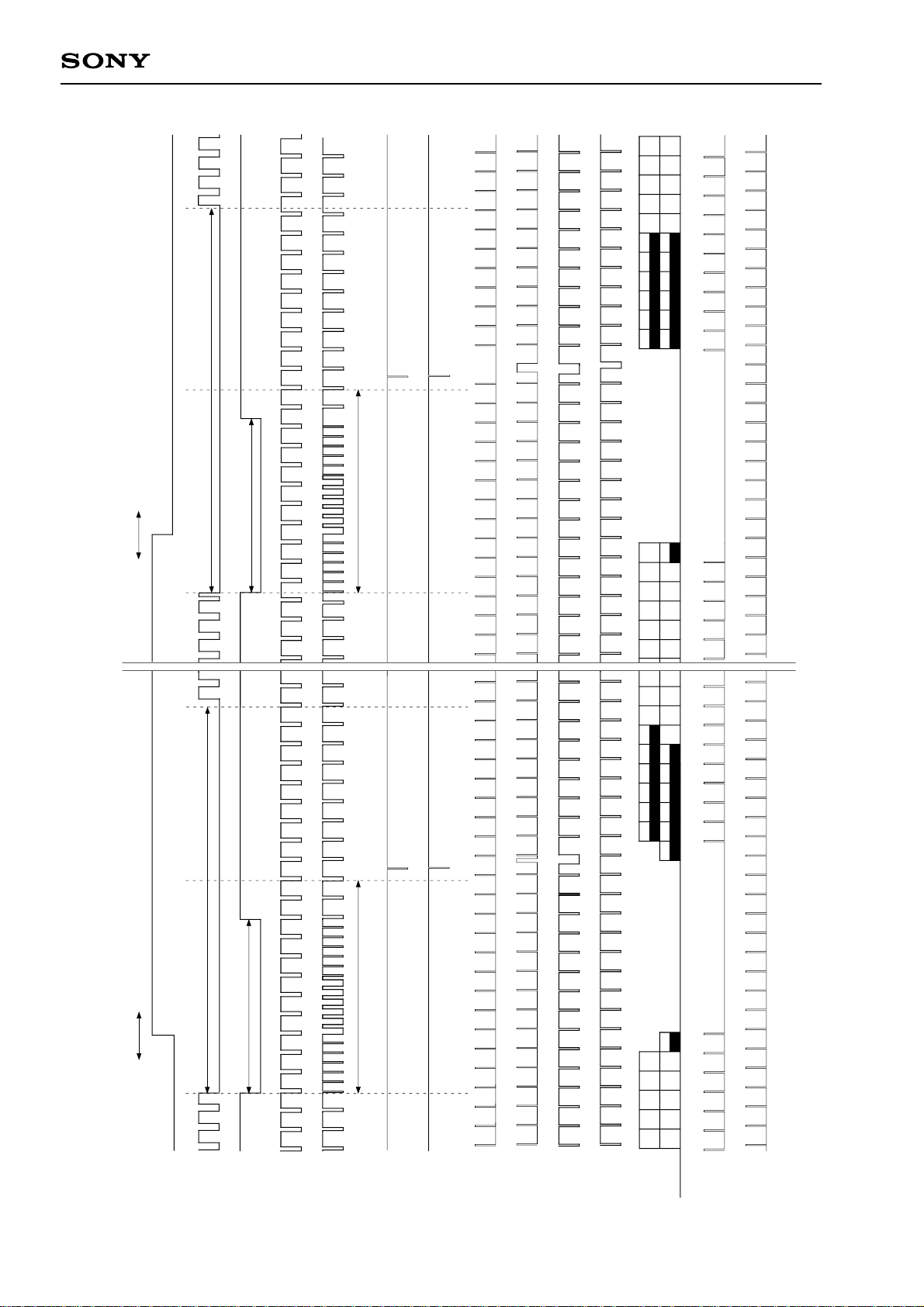
20H
CXD2409R
864210
75319
EVEN FIELD
ODD FIELD
20H
9H
10.5H
486 488 490 492
485 487 489 491
484482
483
624
7135
ODD FIELD
EVEN FIELD
BLK
Timing Chart (1) EIA Vertical Direction
FLD
9H
VD
HD
SYNC
11H
XSG1
XSG2
– 18 –
XV1
XV2
XV3
491
489
487
485
483
XV4
492
490
488
486
484
OUT
CLP1
CCD
CLP2
Page 19
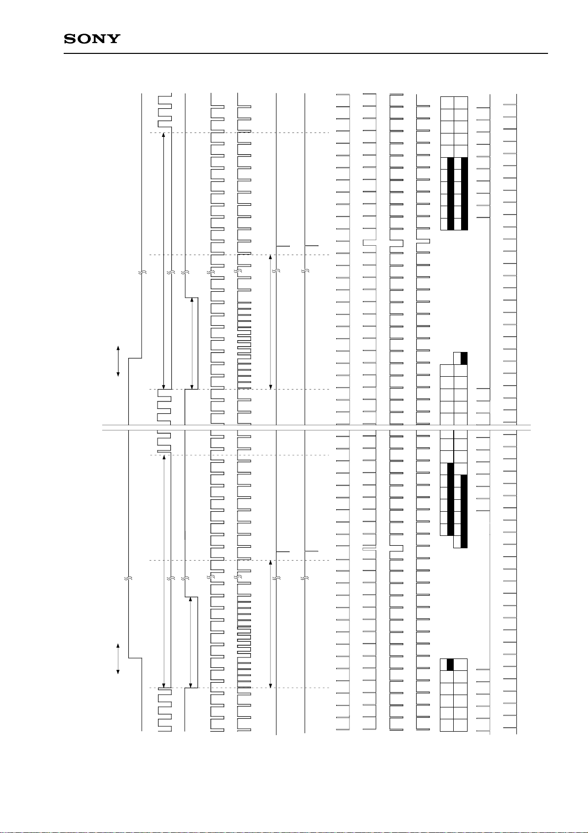
EVEN FIELD
25H
7.5H
15H
CXD2409R
75319
864210
ODD FIELD
ODD FIELD
25H
7.5H
15.5H
582
580
578576
574
62 4
583
581
579
577
575
7531
EVEN FIELD
BLK
FLD
Timing Chart (2) CCIR Vertical Direction
VD
HD
SYNC
XSG1
– 19 –
XSG2
XV1
XV2
XV3
XV4
582580578576574
CCD
575 579 581
573 577 583
OUT
CLP1
CLP2
Page 20
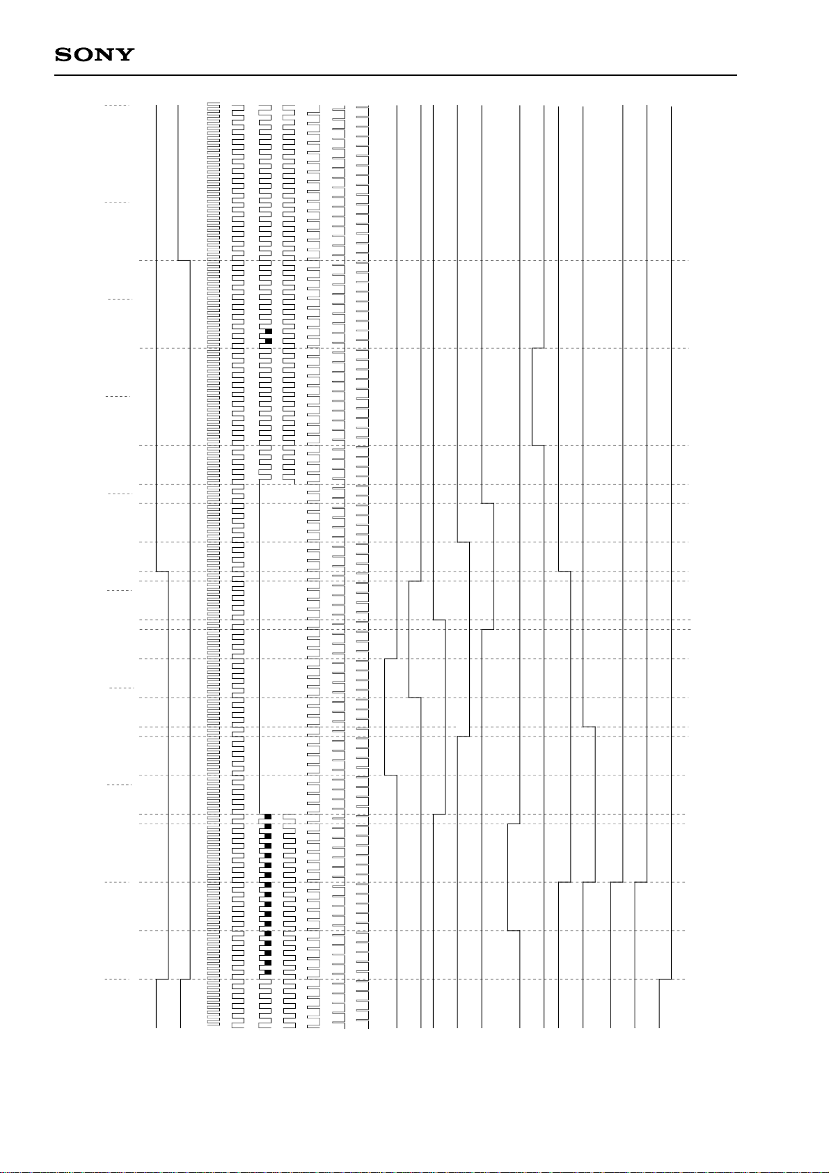
CXD2409R
CL = 6.75MHz : 148.148ns
74
42
55 65
51
37
33
49
45
42
36
10 20 30 40 50 60 70 80 900
BLK
HD
Timing Chart (3) EIA Horizontal Direction
MCK
(CL)
H1
29 41
10
HSYNC
EQ
26
FLD
VSYNC
VD
25
21
XV2
17
XV3
XV4
516
CLP1
XSUB
CLP2
17
SHP
H2
RG
SHD
XV1
– 20 –
Page 21
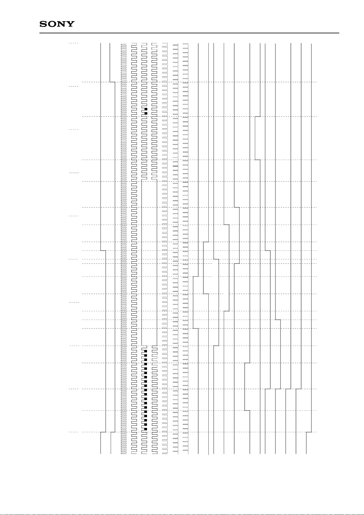
CL = 6.75MHz : 148.148ns
CXD2409R
81
73
63
58
52
48
42
20
44
40
32
24 36
20
39
28
16
42
26
10 20 30 40 50 60 70 80 900
Timing Chart (4) CCIR Horizontal Direction
HD
BLK
MCK
(CL)
H1
H2
RG
SHP
– 21 –
SHD
XV1
XV2
XV3
XV4
XSUB
5
CLP1
CLP2
10
HSYNC
EQ
VSYNC
FLD
VD
Page 22
CL = 6.75MHz : 148.148ns
CXD2409R
429CK
327
208CK (30.8µs)
14CK (2.07µs)
17CK (2.52µs)
296 313
11CK (1.63µs)
17CK (2.52µs)
268 285
9CK (1.33µs)
2CK (0.296µs)
42
68CK (10.1µs)
257
259
257
41
208CK (30.8µs)
259
327
45
37
0
HD
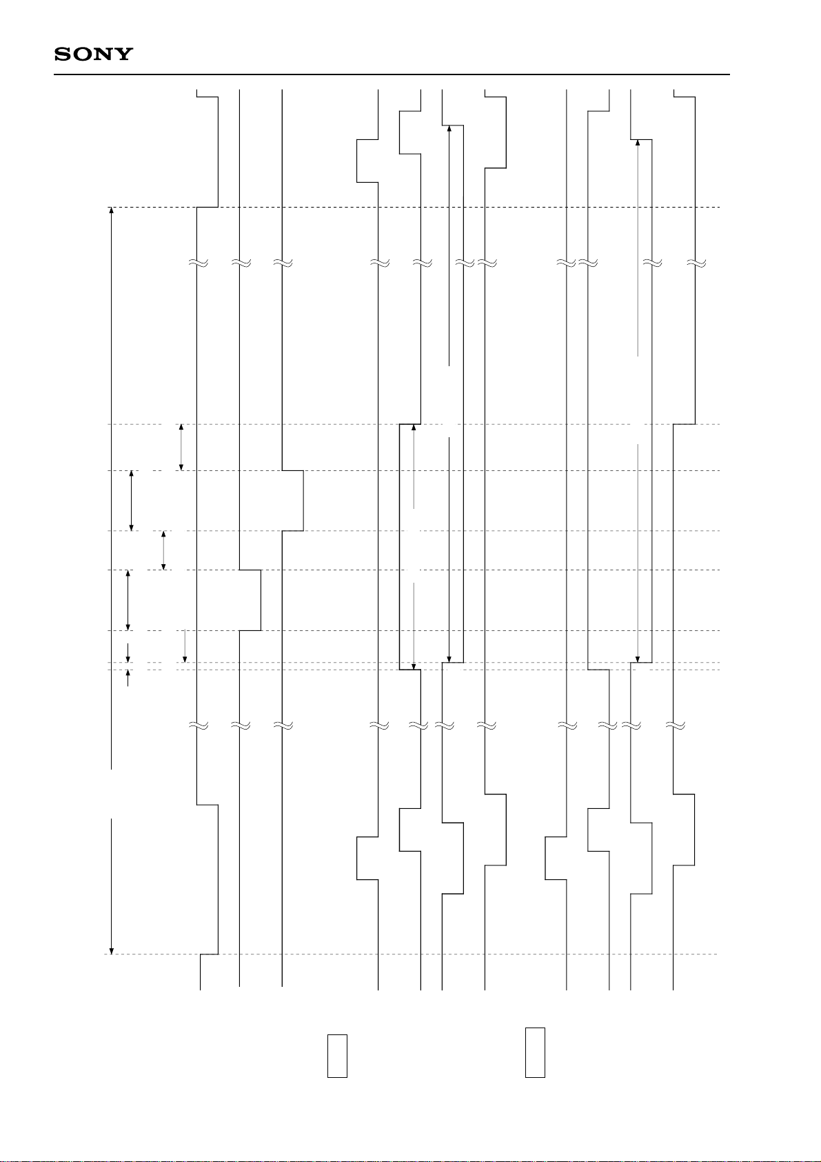
Timing Chart (5) EIA Charge Readout Timing
XSG1
XSG2
ODD
21 33
XV1
– 22 –
29 41
XV2
17 37
XV3
25 45
XV4
EVEN
21 33
XV1
29
XV2
17
XV3
25
XV4
Page 23
CL = 6.75MHz : 148.148ns
CXD2409R
432CK
329
259
44
212CK (31.4µs)
261
40
212CK (31.4µs)
14CK (2.07µs)
17CK (2.52µs)
298
287
11CK (1.63µs)
17CK (2.52µs)
270
9CK (1.33µs)
2CK (0.296µs)
42
36
68CK (10.1µs)
259
44
261
40
329
0
HD
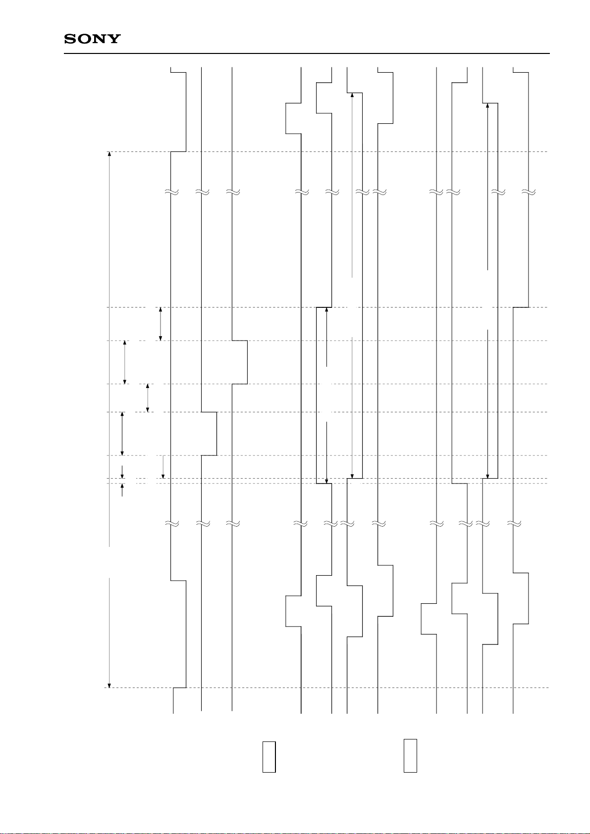
Timing Chart (6) CCIR Charge Readout Timing
XSG1
XSG2
ODD
24
XV1
– 23 –
32
XV2
20
XV3
28 48
XV4
EVEN
24 36
XV1
32
XV2
20
XV3
28 48
XV4
Page 24
CL = 6.75MHz : 148.148ns
10CK
CXD2409R
1/2H
10CK (1.484µs)
10CK
32CK (4.74µs)
16CK (2.370µs)
74CK (10.963µs)
42CK (6.222µs)
32CK (4.74µs)
42CK (6.222µs)
81CK (12.000µs)
32CK (4.74µs)
16CK (2.370µs)
32CK (4.74µs)
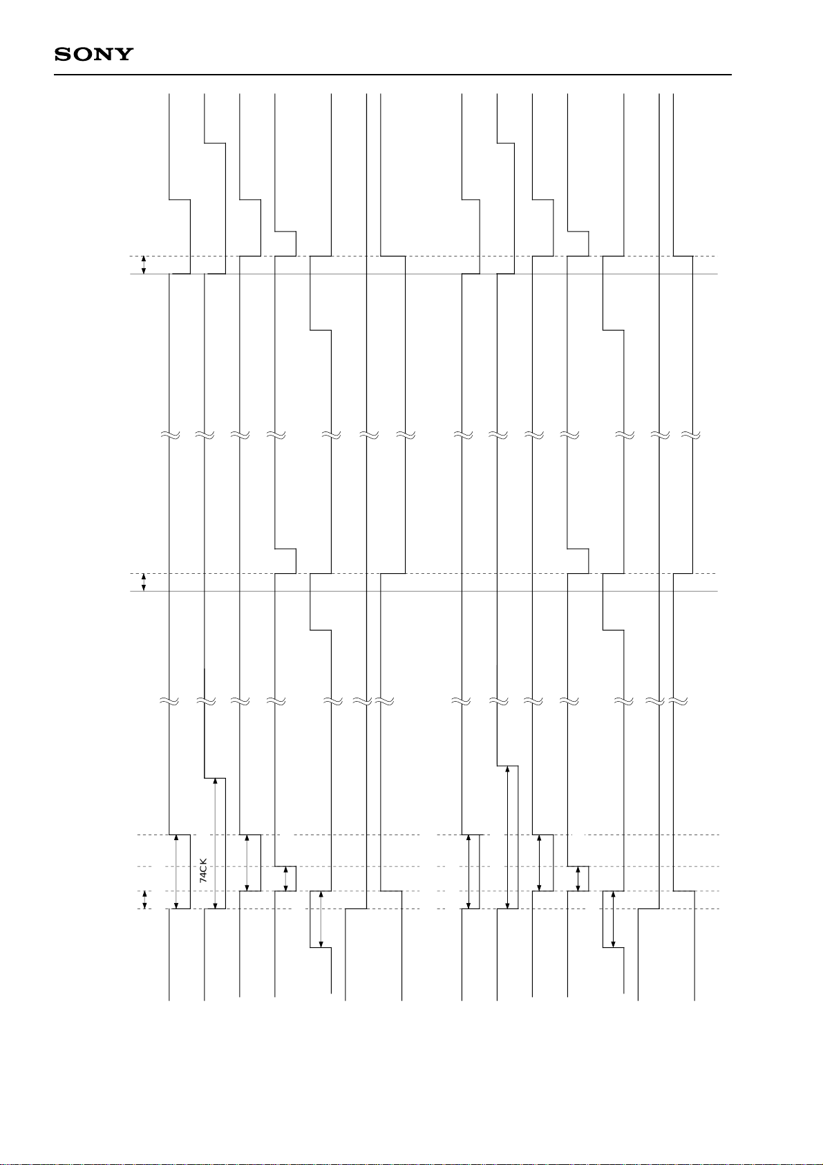
Timing Chart (7) H Effective Period
EIA
HDO
BLKO
HSYNC
EQ
VSYNC
VD
FLD
– 24 –
CCIR
HDO
BLKO
HSYNC
EQ
VSYNC
VD
FLD
Page 25
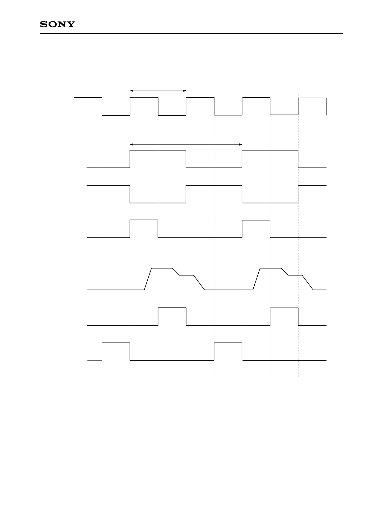
Timing Chart (8) TS + SG High Speed Phase Timing Chart
74.074ns for both EIA and CCIR
CK
148.148ns for both EIA and CCIR
H1
H2
CXD2409R
RG
CCD OUT
SHP
SHD
– 25 –
Page 26
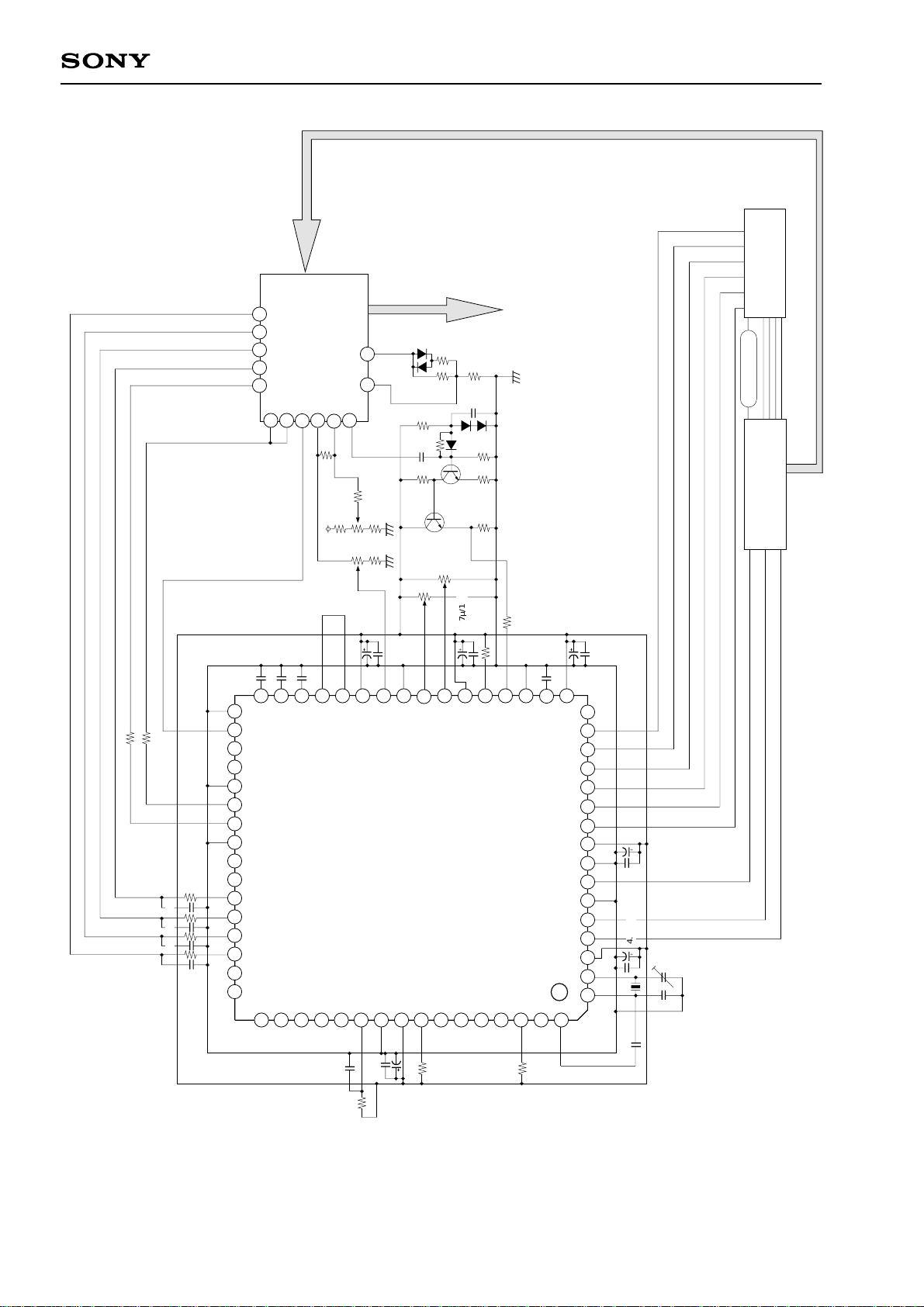
CXD2409R
CXD1267N
100
100
2.2k 2.2k2.2k
+5V
2.2k
GND
47P 47P 47P 47P
29
4
25
50k
SPUPV
39k
10k
24
10k
1k
10k
2SC2785
SPDNV
50k
23
4.7µ/10V
30
25
24
10µ
32
33
34
35
36
37
38
39
40
4142
20
21
10µ
31
CXA1310AQ
161718
10µ
30
13
DET OUT
19
OP+
IRIS
27
1M
10k
+5V
2k
1k
2.7k
50k
4.7µ/10V
0.1µ
0.68µ
27
28
29
26
CXD2409R
43
44
45
46
47
48
52
50
49
51
54
53
57
58
55
56
0.1µ
59
10k
100k
10k
10k
2SC2785
10k
36k
0.1µ
21
22
60
VIDEO OUT
3.9k
19
20
62
61
10k
CCD out
VSUB ADJ
180K-pixel B/W CCD
0.1µ
4.7µ/10V
15µ
17
18
16
14 15
13
12
11
10
9
8
7
6
5
4
3
0.1µ
2
1
64
63
4.7µ/10V
4.7µ/10V
20P
12P
1000P
Application Circuit -EIA-
• Electronic iris mode
• High speed shutter limit: 1/30000s
• Full measurement
• AGC flickerless mode
100k
4.7µ/10V
– 26 –
Application circuits shown are typical examples illustrating the operation of the devices. Sony cannot assume responsibility for
any problems arising out of the use of these circuits or for any infringement of third party patent and other right due to same.
Page 27
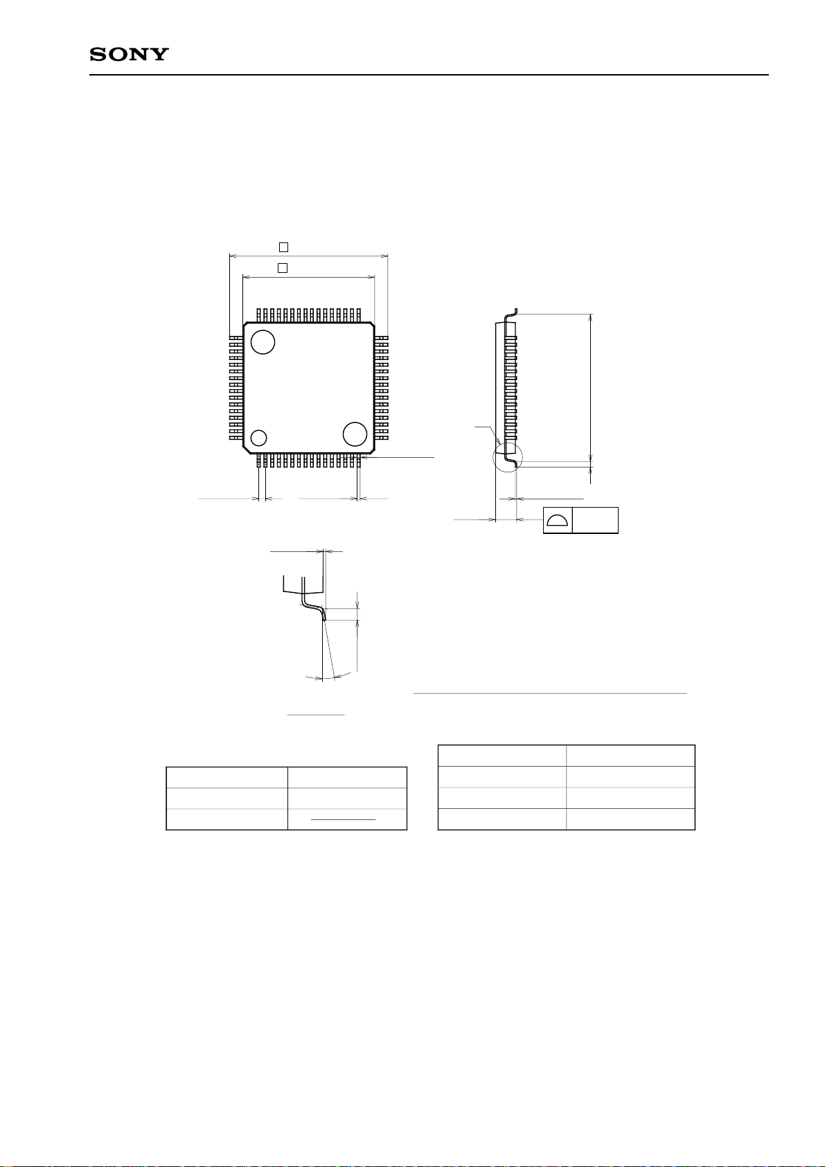
Package Outline Unit: mm
∗ 10.0 ± 0.1
CXD2409R
64PIN LQFP (PLASTIC)
12.0 ± 0.2
49
64
0.5 ± 0.08
48
1
0° to 10°
0.18 – 0.03
0.1 ± 0.1
DETAIL A
+ 0.08
33
0.5 ± 0.2
16
32
(11.0)
A
17
(0.22)
0.5 ± 0.2
+ 0.05
+ 0.2
1.5 – 0.1
0.127 – 0.02
0.1
NOTE: Dimension “∗” does not include mold protrusion.
SONY CODE
EIAJ CODE
JEDEC CODE
LQFP-64P-L01
LQFP064-P-1010
PACKAGE STRUCTURE
PACKAGE MATERIAL
LEAD TREATMENT
LEAD MATERIAL
PACKAGE MASS
– 27 –
EPOXY RESIN
SOLDER/PALLADIUM
42/COPPER ALLOY
0.3g
PLATING
 Loading...