

Page 1

10-bit 20MSPS Video A/D Converter
Description
The CXD2310AR is a 10-bit CMOS A/D converter
for video applications. This IC is ideally suited for the
A/D conversion of video signals in TVs, VCRs,
camcorders, etc.
Features
• Resolution: 10-bit ±1.0 LSB (D.L.E.)
• Maximum sampling frequency: 20MSPS
•
Low power consumption: 150mW (at 20MSPS typ.)
(Not including refer
• TTL compatible input
• Tri-state TTL compatible output (DVDD = 3.3V)
• Low input capacitance
• Reference impedance: 280Ω (typ.)
ence current)
CXD2310AR
48 pin LQFP (Plastic)
Structure
Silicon gate CMOS IC
Absolute Maximum Ratings (Ta = 25°C)
• Supply voltage VDD 7V
•Reference voltage VRT, VRB VDD + 0.5 to VSS – 0.5 V
• Input voltage (analog) VIN VDD + 0.5 to VSS – 0.5 V
• Input voltage (digital) VIH, VIL VDD + 0.5 to VSS – 0.5 V
• Output voltage (digital) VOH, VOL VDD + 0.5 to VSS – 0.5 V
• Storage temperature Tstg –55 to +150 °C
Recommended Operating Conditions
• Supply voltage AVDD, AVSS 5.0 ± 0.25 V
DVDD, DVSS 3.0 to 5.25 V
| DVSS – AVSS | 0 to 100 mV
• Reference input voltage VRB More than 1.8 V
VRT to AVDD – 0.4 V
• Analog input VIN More than 1.8Vp-p
• Clock pulse width TPW1 25 (min.) ns
TPW0 25 (min.) ns
• Operating ambient temperature
Topr –20 to +75 °C
Sony reserves the right to change products and specifications without prior notice. This information does not convey any license by
any implication or otherwise under any patents or other right. Application circuits shown, if any, are typical examples illustrating the
operation of the devices. Sony cannot assume responsibility for any problems arising out of the use of these circuits.
– 1 –
E95429B5X-PK
Page 2
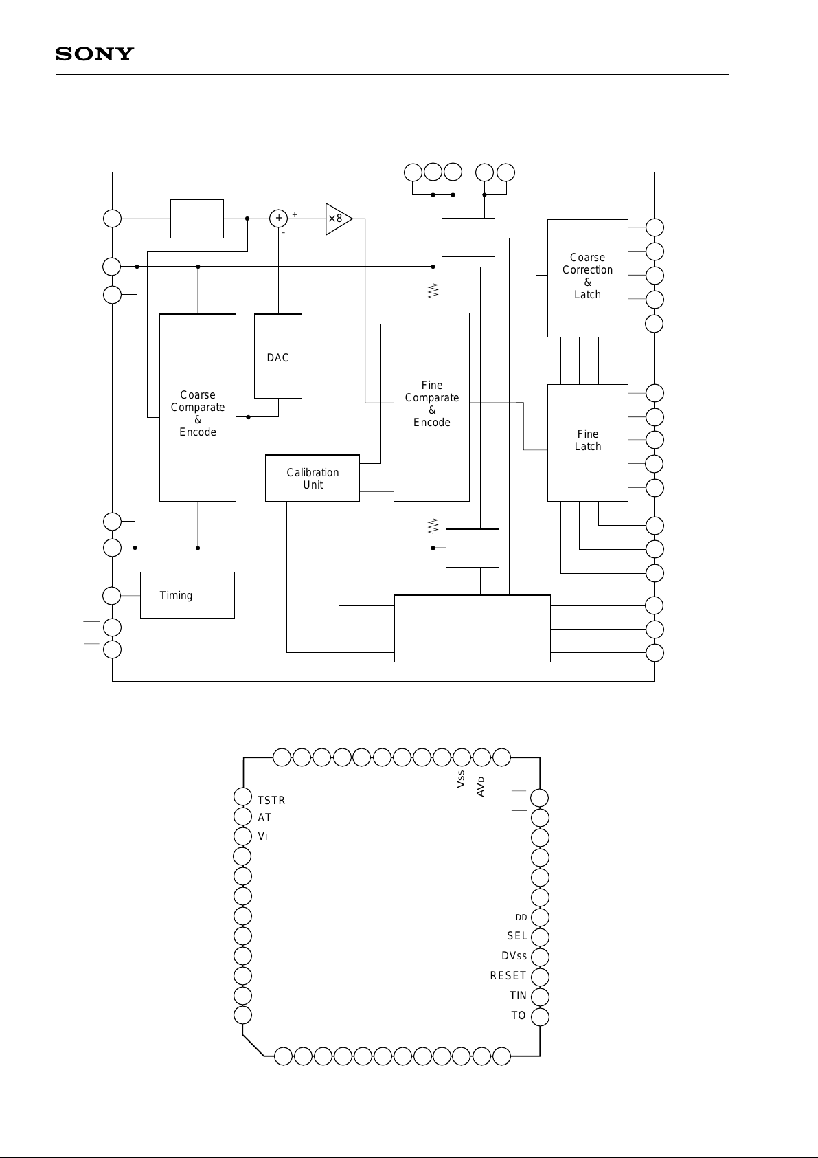
Block Diagram
A
A
A
A
A
A
A
A
A
A
A
A
A
A
A
CXD2310AR
V
VRT
VRT
VRB
VRB
CLK
OE
CE
AVSS
28
27
IN
39
29
30
S/H
Amp
AA
Coarse
AA
Comparate
&
AA
Encode
AA
AA
34
35
22
23
24
Timing Gen
+
DAC
A
+
–
Calibration
Unit
AA
× 8
A
Fine
Comparate
A
&
Encode
A
A
A
Auto Calibration
AAA
Pulse Generator
36
Sense
Amp
Sense
A
Amp
AVDD
18
26
Coarse
AA
Correction
&
Latch
AA
AA
AA
Fine
Latch
AA
AA
D9
12
D8
11
10
D7
D6
9
D5
8
D4
5
4
D3
D2
3
2
D1
D0 (LSB)
1
MINV
21
LINV
20
19
TESTMODE
CAL
41
SEL
17
RESET
15
Pin Configuration
37
38
39
40
41
42
43
44
45
46
47
48
36
TSTR
AT
VIN
NC
CAL
TS
AV
SS
AVSS
DVDD
NC
NC
DV
SS
35
SS
VRB
AV
D1
D0
1
2
34
VRB
3
D2
33
32
31
30
29
NC
NC
NC
D4
D3
6
5
4
– 2 –
SS
DV
7
VRT
DD
DV
VRT
D5
8
28
27
SS
AV
D6
9
10
26
25
SS
DD
DD
AV
AV
AV
CE
OE
CLK
MINV
LINV
TESTMODE
AV
SEL
DV
RESET
TIN
TO
D8
D7
D9
12
11
DD
SS
24
23
22
21
20
19
18
17
16
15
14
13
Page 3
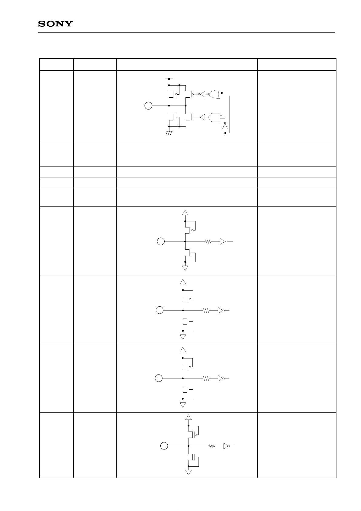
Pin Description
Pin No Symbol Equivalent circuit Description
DVDD
CXD2310AR
1 to 5
8 to 12
13
7, 45
6, 16, 48
27, 28, 36,
43, 44
17 SEL
D0 to D9
TO
DVDD
DVSS
AVSS
DVSS
17
D0 (LSB) to D9 (MSB)
output.
Test pin.
TS = High:
High impedance state
Digital VDD.
Digital VSS.
Analog VSS.
AVDD
Calibration input pulse
select after completion of
the startup calibration.
High : Internal pulse
generation
Low : External input
AVSS
22 CLK
CAL41
15 RESET
41
22
15
AVDD
Clock pin.
AVSS
AVDD
Calibration pulse input.
AVSS
AVDD
Calibration circuit reset
and startup calibration
restart.
AVSS
– 3 –
Page 4
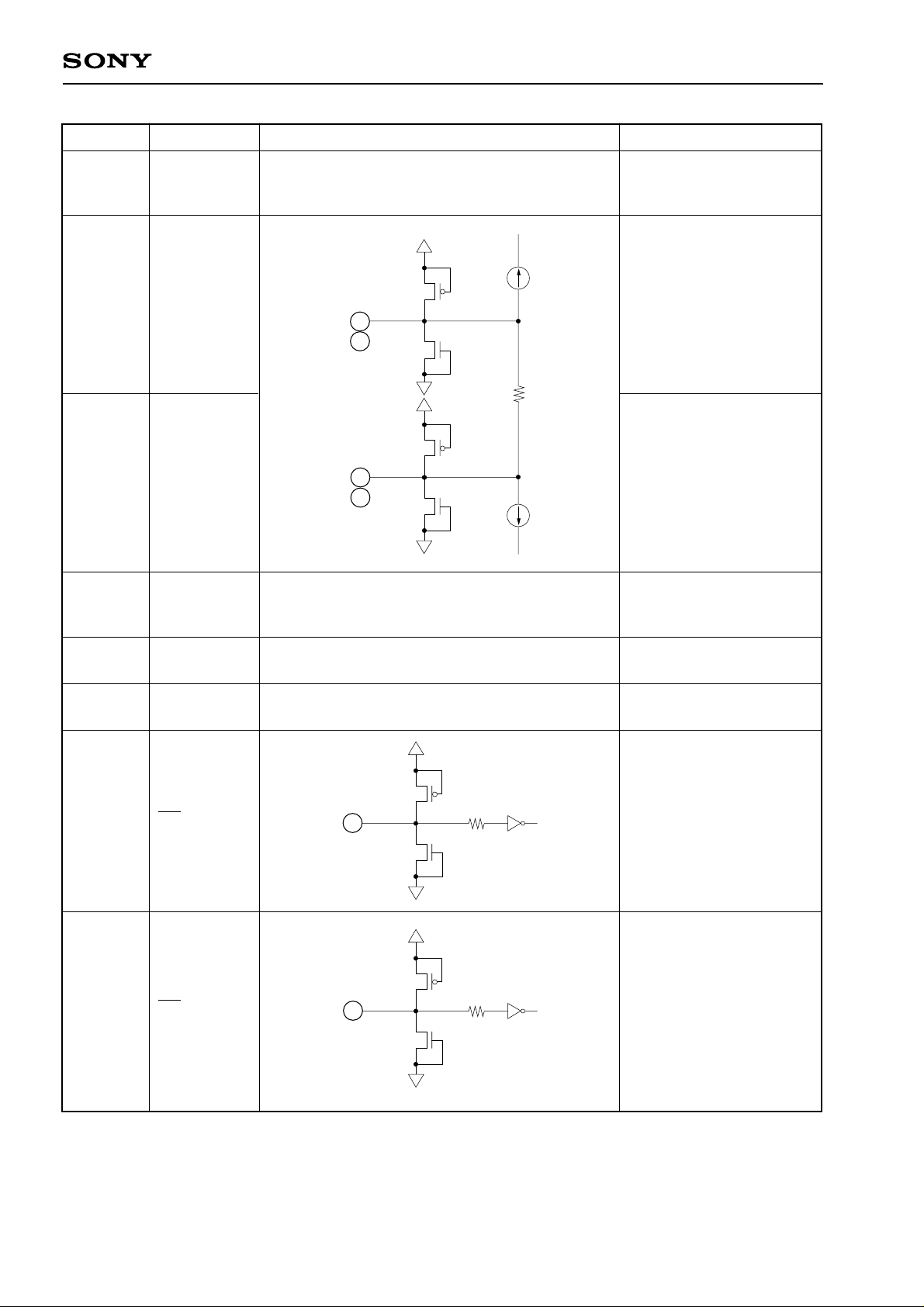
Pin No. Symbol Equivalent circuit Description
Test signal input.
14 TIN
Normally fixed to AVDD or
AVSS.
AVDD
CXD2310AR
29, 30 VRT
34, 35 VRB
38 AT
42 TS
37 TSTR
29
30
34
Reference top.
AVSS
Reference bottom.
35
Test signal output.
TS = High:
High impedance state
Test signal input.
Normally fixed to AVDD.
Test signal input.
Normally fixed to AVSS.
AVDD
23 OE
CE24
23
24
D0 to D9 output enable.
Low : Output state
High : High impedance
state
AVSS
AVDD
Chip enable.
Low : Active state
High : Standby state
AVSS
– 4 –
Page 5
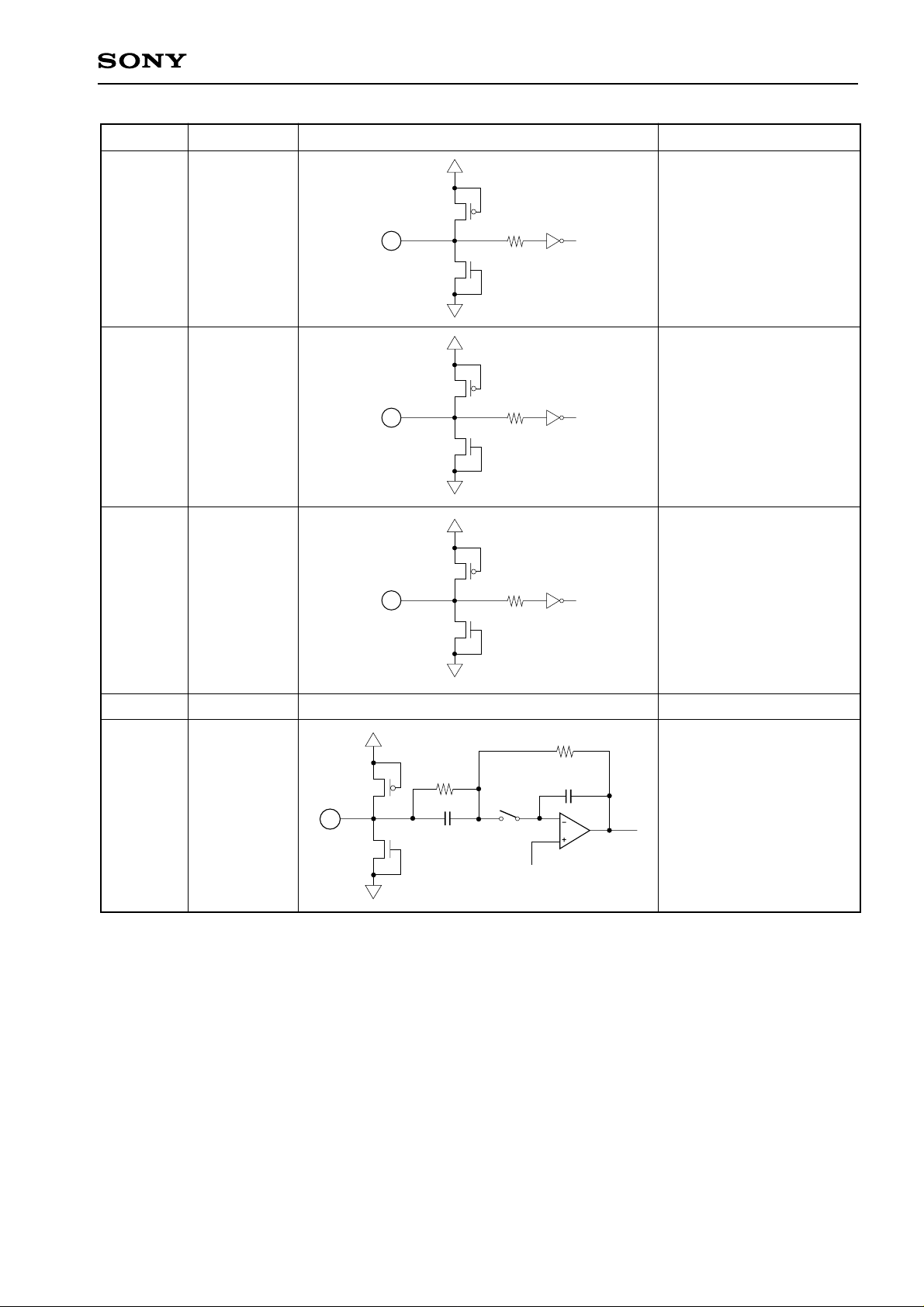
Pin No. Symbol Equivalent circuit Description
AVDD
Test mode.
19 TESTMODE
19
High : Output state
Low : Output fixed
AVSS
AVDD
Output inversion.
20
LINV
20
High : D0 to D8 are
inverted and
output.
AVSS
CXD2310AR
21 MINV
18, 25, 26 AVDD
39 VIN
AVDD
39
AVSS
21
AVDD
Output inversion.
High : D9 is inverted and
output.
AVSS
Analog VDD.
Analog input.
– 5 –
Page 6

Digital Output
The following table shows the correlation between the analog input voltage and the digital output code
(TESTMODE = 1, LINV, MINV = 0)
CXD2310AR
Input signal voltage
VRT
VRB
Step
0
511
512
1023
Digital output code
MSB LSB
1 1 1 1 1 1 1 1 1 1
1 0 0 0 0 0 0 0 0 0
0 1 1 1 1 1 1 1 1 1
0 0 0 0 0 0 0 0 0 0
The following table shows the output state for the combination of TESTMODE, LINV, and MINV states.
TESTMODE
1
1
1
1
0
0
0
0
LINV MINV D0 D1 D2 D3 D4 D5 D6 D7 D8 D9
0
1
0
1
0
1
0
1
0
P
P
P
P
P
P
P
P
0
N
N
N
N
N
N
N
N
1
P
P
P
P
P
P
P
P
1
N
N
N
N
N
N
N
N
0
1
0
1
0
1
0
1
0
0
0
1
0
1
0
1
0
1
1
1
0
1
0
1
0
1
0
1
0
1
0
1
0
1
0
1
P
P
P
N
N
P
N
N
0
1
0
0
1
1
1
0
P: Forward-phase output N: Inverted output
Timing Chart 1
Analog input
Data output
Timing Chart 2
Output enable (OE)
Clock
tSD
tPW1
1.65V
N
tDL
1.65V (DVDD = 3.3V)
2.5V (DVDD = 5.0V)
1.65V
t
PW0
N + 1
N + 2
N – 3 N – 2 NN – 1
: Indicates point at which analog data is sampled
t
PEZ tPZE
1.65V (DVDD = 3.3V)
2.5V (DVDD = 5.0V)
1.65V
N + 3
N + 4
Data output
Active Active
High Impedance
– 6 –
Page 7
CXD2310AR
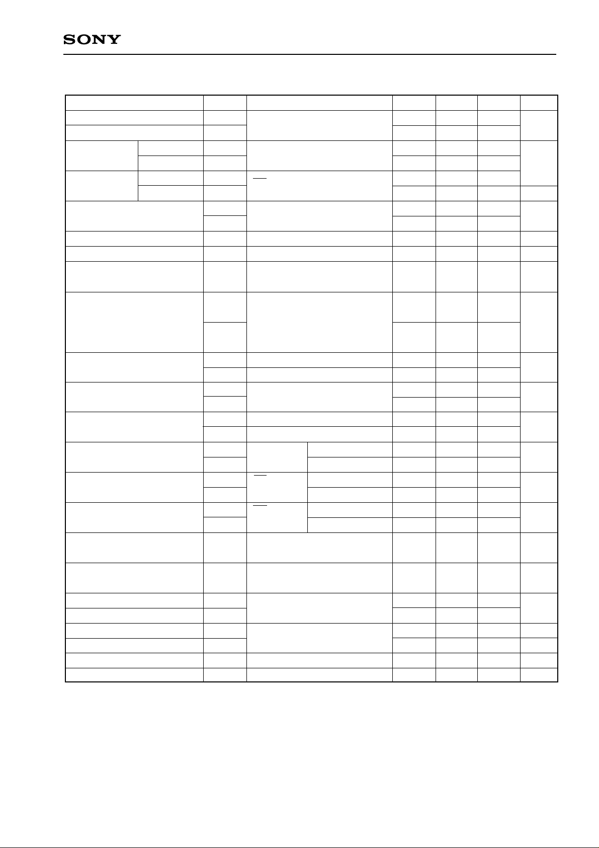
Electrical Characteristics
Item
Max. conversion rate
Min. conversion rate
Supply
current
Standby
current
Reference pin current
Analog input band
Analog input capacitance
Reference resistance value
(VRT – VRB)
Offset voltage
Startup calibration start
voltage
Digital input voltage
Analog input current
Digital input current
Digital output current
Digital output current
Tri-state output disable time
Analog
Digital
Analog
Digital
(Fc = 20MSPS, AVDD = 5V, DVDD = 3.3V, VRB = 2.0V, VRT = 4.0V, Ta = 25°C)
Symbol Conditions Min. Typ. Max. Unit
Fc max
Fc min
IADD
IDDD
IAST
IDST
IRT
IRB
BW
CIN
RREF
EOT
EOB
VCAL1
VCAL2
VIH
VIL
AIH
AIL
IIH
IIL
IOH
IOL
IOZH
IOZL
tPEZ
FIN = 1.0kHz
triangular wave input
FIN = 1.0kHz
triangular wave input
CE = High
–1dB
EOT = theoretical value-actual
measured value
EOB = actual measured valuetheoretical value
AVDD – AVSS
VRT – VRB
AVDD = 4.75V to 5.25V
VIN = 4V
VIN = 2V
DVDD = max
OE = AVSS
DVDD = min
OE = AVDD
DVDD = max
Clock not synchronized for
active →high impedance
VIH = DVDD
VIL = 0V
VOH = DVDD – 0.5V
VOL = 0.4V
VOH = DVDD
VOL = 0V
20
20
5.0
–11.0
180
40
–120
2.3
–50
3.5
3.5
20
27
3.0
7.0
–7.0
70
9
280
90
–70
2.5
1.0
40
–40
25
0.5
34
5
1.0
1.0
11.0
–5.0
380
140
–20
0.8
50
5
5
1
1
30
MSPS
mA
µA
mA
MHz
pF
Ω
mV
V
V
µA
µA
mA
µA
ns
Tri-state output enable time
Integral non-linearity error
Differential non-linearity error
Differential gain error
Differential phase error
Output data delay
Sampling delay
tPZE
EL
ED
DG
DP
tDL
tSD
Clock not synchronized for high
impedance → active
NTSC 40 IRE mod
ramp, Fc = 14.3MSPS
CL = 20pF
– 7 –
10
15
±1.3
±0.5
1.0
0.3
8
2
13
4
20
±2.0
±1.0
18
6
ns
LSB
%
deg
ns
ns
Page 8

CXD2310AR
Item
Symbol Conditions Min. Typ. Max. Unit
FIN = 100kHz
FIN = 500kHz
SNR
SNR
FIN = 1MHz
FIN = 3MHz
FIN = 7MHz
FIN = 10MHz
FIN = 100kHz
FIN = 500kHz
SFDR
SFDR
FIN = 1MHz
FIN = 3MHz
FIN = 7MHz
FIN = 10MHz
Application Circuit 1. Startup calibration + internal auto calibration
4.0V
53
52
53
54
47
45
60
59
60
65
50
49
dB
dB
4.0V
2.0V
2.0V
AV
AV
AVSSDVDD
DVSS
DD
SS
39
40
41
42
43
44
45
46
47
48
37
38
TSTR
AT
VIN
NC
CAL
TS
AVSS
AVSS
DVDD
NC
NC
SS
DV
36
AVDD
34
3
33
VRB
D2
32
31
30
29
NC
NC
NC
VRT
VRT
DD
SS
D3
5
4
D4
DV
DV
D5
7
6
8
35
SS
VRB
AV
D0
D1
1
2
28
SS
AV
D6
9
26
27
SS
DD
AV
AV
TESTMODE
D7
D8
10
11
25
DD
AV
CE
OE
CLK
MINV
LINV
AVDD
SEL
DVSS
RESET
TIN
TO
D9
12
24
23
22
21
20
19
18
17
16
15
14
13
AVSS
AVSS
DVSS
Clock input
AVDD
AVDD
is all 0.1µF
Digital output
Application circuits shown are typical examples illustrating the operation of the devices. Sony cannot assume responsibility for
any problems arising out of the use of these circuits or for any infringement of third party patent and other right due to same.
– 8 –
Page 9
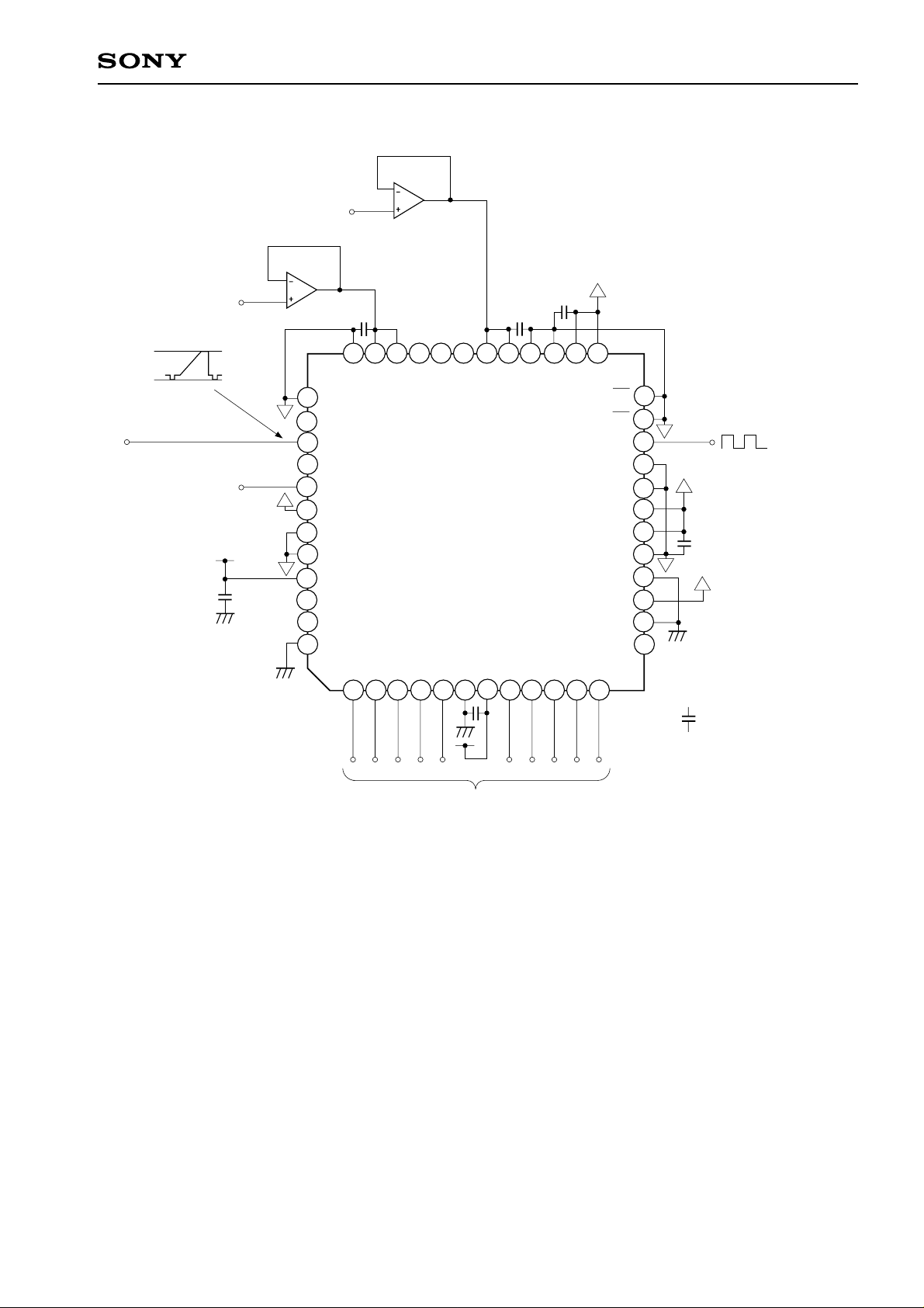
Application Circuit 2. Startup calibration + external sync calibration
4.0V
CXD2310AR
4.0V
2.0V
Calibration pulse
2.0V
AV
AV
AVSSDVDD
DVSS
DD
SS
45
39
40
41
42
43
44
46
47
48
37
38
TSTR
AT
VIN
NC
CAL
TS
AVSS
AVSS
DVDD
NC
NC
SS
DV
36
1
SS
AV
D0
35
VRB
D1
2
34
VRB
3
D2
33
4
NC
D3
32
5
NC
D4
31
AVDD
30
29
VRT
DD
DV
VRT
D5
8
SS
AV
D6
9
NC
SS
DV
7
6
SS
DD
AV
AV
TESTMODE
D7
D8
10
11
25
DD
AV
CE
OE
CLK
MINV
LINV
AVDD
SEL
DVSS
RESET
TIN
TO
D9
12
19
17
16
15
14
24
23
22
21
20
18
13
AVSS
AVSS
DVSS
Clock input
AVDD
AVDD
26
27
28
is all 0.1µF
Digital output
Application circuits shown are typical examples illustrating the operation of the devices. Sony cannot assume responsibility for
any problems arising out of the use of these circuits or for any infringement of third party patent and other right due to same.
– 9 –
Page 10
CXD2310AR
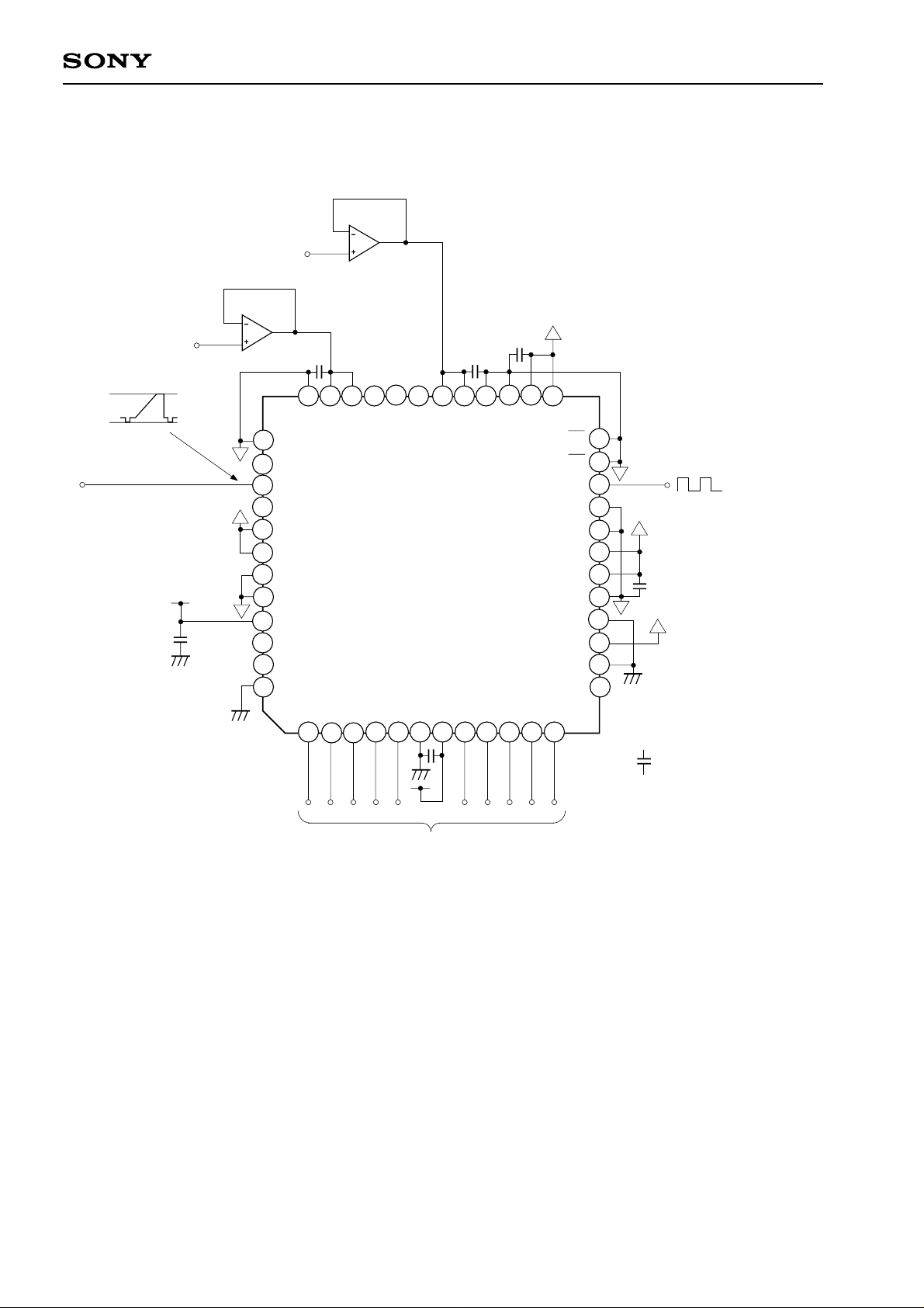
Application Circuit 3. Only startup calibration
(Less than supply voltage fluctuation range of AVDD = ±100mV and reference voltage fluctuation range of
|VRT – VRB| = 200mV)
4.0V
4.0V
2.0V
2.0V
AV
AV
AVSSDVDD
DVSS
DD
SS
45
46
47
37
38
39
40
41
42
43
44
48
TSTR
AT
VIN
NC
CAL
TS
AVSS
AVSS
DVDD
NC
NC
SS
DV
36
AVDD
34
3
VRB
D2
33
4
NC
D3
32
31
30
29
NC
NC
D4
6
5
SS
DV
VRT
DD
DV
7
VRT
D5
8
35
SS
VRB
AV
D0
D1
1
2
28
SS
AV
D6
9
26
27
SS
DD
AV
AV
TESTMODE
D7
D8
10
11
25
DD
AV
CE
OE
CLK
MINV
LINV
AVDD
SEL
DVSS
RESET
TIN
TO
D9
12
23
20
19
18
17
16
15
14
24
22
21
13
AVSS
AVSS
DVSS
Clock input
AVDD
AVDD
is all 0.1µF
Digital output
Application circuits shown are typical examples illustrating the operation of the devices. Sony cannot assume responsibility for
any problems arising out of the use of these circuits or for any infringement of third party patent and other right due to same.
– 10 –
Page 11
CXD2310AR
1. Calibration Function
In order to achieve superior linearity, the CXD2310AR has a built-in calibration circuit. In order to eliminate the
necessity for the externally input calibration pulse required by the earlier CXD2310R, a startup calibration
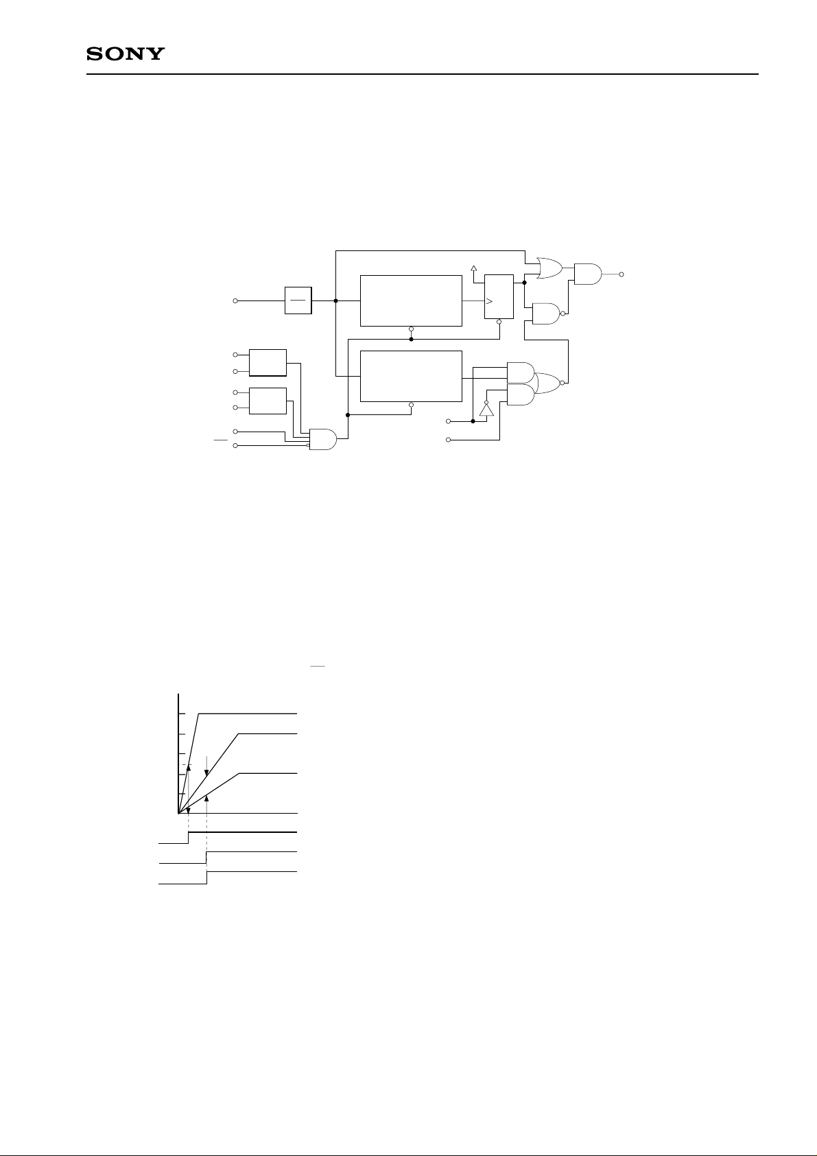
function and an auto calibration pulse generation function have been newly added to the CXD2310AR. Fig. 1
shows a block diagram of the calibration pulse generation circuit.
AVDD
D
CLK
16
1
14 bit
Counter
CLR
CO
Q
CLR
OUT
AVDD
AVSS
VRT
VRB
RESET
CE
Sence
Amp 1
Sence
Amp 2
24 bit
Counter
CLR
CO
SEL
CAL
Fig. 1. Calibration Pulse Generation Circuit
(1) Startup Calibration Function
Over 600 calibration pulses are needed to complete the initial calibration process when the power is first
supplied to the IC. The startup calibration function automatically generates these pulses internally and
completes the initial calibration process.
The following five conditions must be satisfied to initiate the
startup calibration function.
When RESET = High and CE = Low
[V]
2.5
DD
5
1V
AV
VRT
VRB
a) The voltage between AVDD and AVSS is approximately
2.5V or more.
b) The voltage between VRT and VRB is approximately 1V
or more.
c) The RESET pin (Pin 15) must is high.
d) The CE pin (Pin 24) must is low.
Sence Amp 1
Sence Amp 2
CLR
0
[ t ]
e) Condition b is met after condition a.
Once all five of these conditions have been met, the calibration
pulses are generated. The pulses are generated by counting 16
main clock cycles on a 14-bit counter and closing the gate when
the carry-out occurs. Therefore, the time required for startup
calibration after the above five conditions have been met is
determined by the following formula:
Startup calibration time = main clock cycle × 16 × 16,384
For example, if the main clock frequency is 14.3MHz, the time required for startup calibration is 18ms.
– 11 –
Page 12
CXD2310AR
(2) Auto Calibration Pulse Generation Function
After startup calibration is completed, this function periodically generates calibration pulses so that calibration
can be performed constantly without any need for input of calibration pulses from an external source. This
function counts 16 main clock cycles on a 24-bit counter and uses the carry-out as the calibration pulse. The
cycle of the calibration pulse generated in this fashion is as follows:
Internal calibration pulse generation cycle = main clock cycle × 16 × 16,777,216
Therefore, if the main clock frequency is 14.3MHz, the calibration pulse cycle is approximately 19 seconds;
since calibration is performed once every seven pulses, the calibration cycle is approximately 130 seconds. In
order to use this function, the SEL pin (Pin 17) must be high.
Note that this function cannot be used if fixing the lower bits in the calibration operation as described below will
cause problems because this function is executed asynchronously without regard to the input signals.
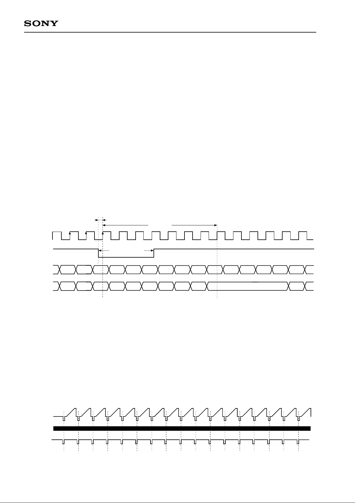
(3) External Calibration Pulse Input Function
If the auto calibration function cannot be used, calibration can be performed in synchronization with the input
signals when a calibration pulse is input from the CAL pin (Pin 41) by setting the SEL pin (Pin 17) low.
10ns or more
7clock
CLK
CAL
D5 to D9
D0 to D4
1clock or more
N – 3
N – 3
N – 2 N – 1
N – 2 N – 1
N N + 1 N + 2 N + 3 N + 4
N
N + 5
N + 5
Fig. 2. Calibration Timing Chart
Calibration starts when the falling edge of the pulse input to the CAL pin (Pin 41) is detected. Because the
lower comparator is occupied for four clock cycles at this point, the previous lower data is held for four clock
cycles after seven clock cycles since the rising edge of the clock cycle in which the falling edge of CAL was
detected. Calibration can be performed outside of video intervals by using the sync signal, etc., to input the
CAL signal. An example of this is shown below.
(1) Inputting CAL every H-sync
Input
CLK
CAL
– 12 –
Page 13
CXD2310AR
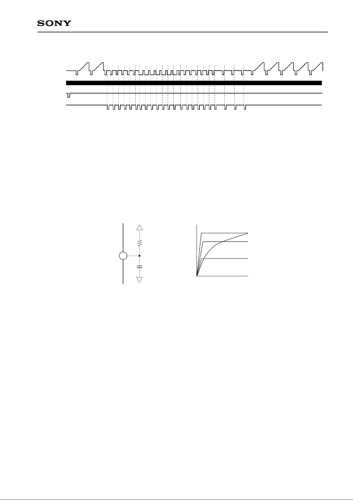
(2) Inputting CAL every V-sync
Input
CLK
RESET
CAL
It is also possible to use only the startup calibration function by leaving the SEL pin (Pin 1/) low and fixing the
CAL pin (Pin 41) either high or low. Note that this method requires restriction of the fluctuation range of the
supply voltage and the reference voltage.
(4) Re-initiating the Startup Calibration Function
The startup calibration function can be re-initiated after the power and reference voltage are supplied by using
the CE pin (Pin 24) and the RESET pin (Pin 15). Particularly in cases where the riseup characteristics of the
power supply and the reference voltage are unstable or the order of the riseup is not kept, it is possible to
initiate startup calibration properly by connecting a CR and delaying startup until after power supply riseup.
[V]
AV
VRT
DD
RESET
VRB
[ t ]
RESET
AVDD
R
15
C
AVSS
Fig. 3. Initiation of the Startup Calibration Function Using the RESET pin
– 13 –
Page 14

CXD2310AR
2. Power supply
To prevent the influence of noise, connect the power supply to a 0.1µF by-pass capacitor as near the device
as possible.
3. DVDD
Either a 3.3V or 5.0V digital power supply can be used. Compared to the 5.0V power supply, the 3.3V power
supply generates a decreased amount of radiation noise but offers a decreased drive capacity. These two
power supplies do not virtually differ in static and dynamic characteristics. Further, the High output level rises
up to DVDD.
4. Reference input
The voltage to be supplied to the reference pins must be driven by a buffer having a 10mA or more drive
capacity. For supplied voltage stabilization, connect the buffer to a 0.1µF by-pass capacitor as near the pins as
possible.
5. Latch-up
Ensure that the AVDD and DVDD pins share the same power supply on a board to prevent latch-up which may
be caused by power ON time-lag.
6. Board
To obtain full-expected performance from this IC, be sure that the mounting board has a large ground pattern
for lower impedance. It is recommended that the IC be mounted on a board without using a socket to evaluate
its characteristics adequately.
– 14 –
Page 15
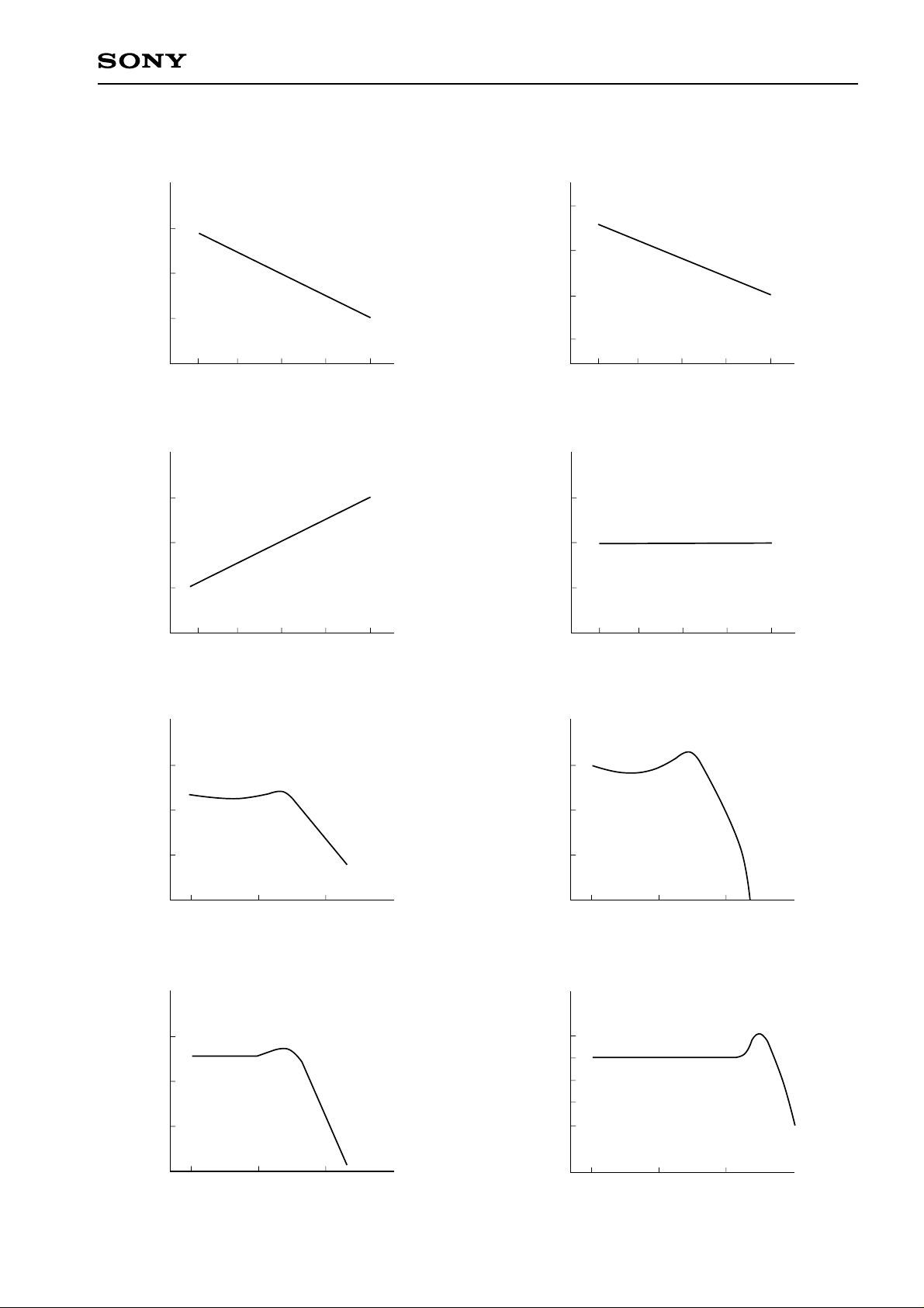
Example of Representative Characteristics
CXD2310AR
Supply current vs. Ambient temperature
Fc = 20MHz
29
28
27
Supply current [mA]
–20 0 25 50 75
Ambient temperature [°C] Ambient temperature [°C]
fin = 1kHz ramp wave
AVDD = 5.0V
DVDD = 3.3V
Output data delay vs Ambient temperature
17
15
13
Output data delay [ns]
AVDD = 5.0V
DVDD = 3.3V
Fc = 1MHz
CL = 20pF
Maximum operating frequency vs.
Ambient temperature
35
30
25
20
Maximum operating frequency [MHz]
–20 0 25 50 75
fin = 1kHz ramp wave
AVDD = 5.0V
DVDD = 3.3V
Sampling delay vs. Ambient temperature
6
4
2
Sampling delay [ns]
AVDD = 5.0V
DVDD = 3.3V
Fc = 1MHz
–20 0 25 50 75
Ambient temperature [°C] Ambient temperature [°C]
Input frequency vs. SNR
60
50
SNR [dB]
40
100k 1M 10M
Input frequency [Hz] Input frequency [Hz]
Input frequency vs. Effective bits
9
8
Effective bits [bit]
7
AVDD = 5.0V
DVDD = 3.3V
Fc = 20MHz
VIN = 2Vp-p
Ta = 25°C
AVDD = 5.0V
DVDD = 3.3V
Fc = 20MHz
VIN = 2Vp-p
Ta = 25°C
–20 0 25 50 75
Input frequency vs. SFDR
60
50
SFDR [dB]
40
100k 1M 10M
1
0
–1
–2
Output level [dB]
–3
AVDD = 5.0V
DVDD = 3.3V
Fc = 20MHz
VIN = 2Vp-p
Ta = 25°C
AVDD = 5.0V
DVDD = 3.3V
Fc = 20MHz
VIN = 2Vp-p
Ta = 25°C
Input band
100k 1M 10M
Input frequency [Hz] Input frequency [Hz]
100k 1M 10M
– 15 –
Page 16
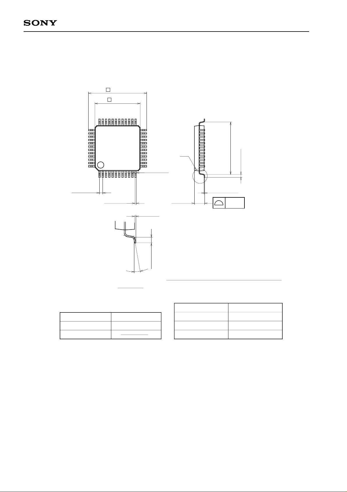
Package Outline Unit : mm
∗ 7.0 ± 0.1
CXD2310AR
48PIN LQFP (PLASTIC)
9.0 ± 0.2
37
48
0.5 ± 0.08
36
1
+ 0.08
0.18 – 0.03
0° to 10°
DETAIL A
25
12
0.1 ± 0.1
24
13
0.5 ± 0.2
A
(0.22)
(8.0)
0.5 ± 0.2
+ 0.05
0.127 – 0.02
+ 0.2
1.5 – 0.1
0.1
NOTE: Dimension “∗” does not include mold protrusion.
SONY CODE
EIAJ CODE
JEDEC CODE
LQFP-48P-L01
LQFP048-P-0707
– 16 –
PACKAGE STRUCTURE
PACKAGE MATERIAL
LEAD TREATMENT
LEAD MATERIAL
PACKAGE MASS
EPOXY RESIN
SOLDER/PALLADIUM
42/COPPER ALLOY
0.2g
PLATING
 Loading...