

Page 1

CXD2301Q
For the availability of this product, please contact the sales office.
8-bit 30MSPS Video A/D Converter with Built-in Amplifier/Clamp
Description
The CXD2301Q is an 8-bit CMOS A/D converter
for video applications with built-in amplifier/syncclamp circuits. A maximum conversion rate of
30MSPS is attained at a low power consumption by
adopting a 2-step parallel system.
Features
• Resolution: 8 bits ±1/2LSB (DL)
• Maximum sampling frequency: 30MSPS
• Low power consumption: 120mW (at 30MSPS
typ.)
(Including reference current)
• Standby function:
0.5mW power consumption in standby
• Amplifier functions:
provided
• Synchronous clamp function
• Clamp ON/OFF function
• Reference voltage self-bias circuit
• TTL compatible output
• 3V digital interface capability
• Single 5V or dual 4.75/3.3V power supplies
• Low input capacitance: 8pF
• Reference impedance: 330Ω (typ.)
Applications
Wide range of application fields where high-speed
A/D conversion is required such as in the digital
systems of TVs, VCRs, etc.
Structure
Silicon gate CMOS IC
Built-in 3x amplifier (15MHz band),
2-input selector function
Absolute Maximum Ratings (Ta = 25°C)
• Supply voltage VDD 7V
•Reference voltage VRT, VRB
• Input voltage (analog) VIN
• Input voltage (digital) VIH, VIL
• Output voltage (digital) VOH, VOL
• Storage temperature Tstg –55 to +150 °C
Recommended Operating Conditions
• Supply voltage IDVSS–AVSSI0 to 100 mV
Single power supply AVDD, DVDD5.0 ± 0.25 V
Dual power supply AVDD 4.75 ± 0.25 V
• Reference input voltage
• Analog input ADIN More than 1.2Vp-p
• Clock pulse width TPWI 16 (min) ns
• Operating ambient temperature
32 pin QFP (Plastic)
VDD +0.5 to VSS –0.5 V
VDD +0.5 to VSS –0.5 V
VDD +0.5 to VSS –0.5 V
VDD +0.5 to VSS –0.5 V
DVDD 3.3 ± 0.3 V
VRB 0 to V
VRT to 2.2 V
TPWO 16 (min) ns
Topr –20 to +75 °C
Sony reserves the right to change products and specifications without prior notice. This information does not convey any license by
any implication or otherwise under any patents or other right. Application circuits shown, if any, are typical examples illustrating the
operation of the devices. Sony cannot assume responsibility for any problems arising out of the use of these circuits.
– 1 –
E92Y50B4X-PK
Page 2
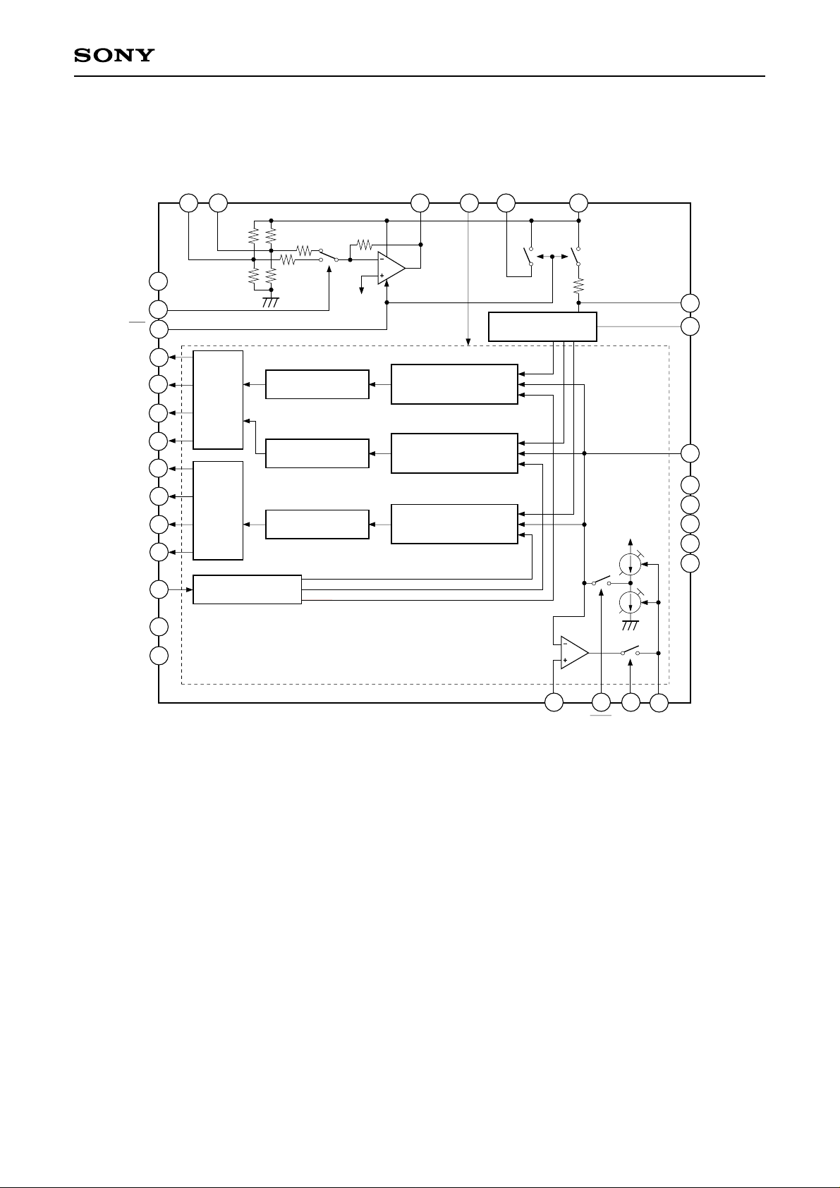
Block Diagram
27
25
30
21
22
CXD2301Q
AVDDADVADVOPOVIN2 VIN1
26
TEST
SS)
(DV
SEL
CE
D0(LSB)
D1
D2
D3
D4
D5
D6
D7(MSB)
CLK
DD
DV
DVSS
19
16
15
14
13
12
11
10
18
17
R
R
4
5
Lower
data
latch
Upper
data
latch
9
Clock generator
8
Lower encoder
(4 bit)
Lower encoder
(4 bit)
Upper encoder
(4 bit)
3R
VBI
A/D Converter
Lower
sampling comparator
(4 bit)
Lower
sampling comparator
(4 bit)
Upper
sampling comparator
(4 bit)
Block
Reference supply
RTS
ADV
23
29
28
31
VRT
VRB
1
ADIN
AVSS
2
AVSS
3
AVSS
7
AVSS
AVSS
24
VREF CLE CLP CCP
6
20
32
– 2 –
Page 3
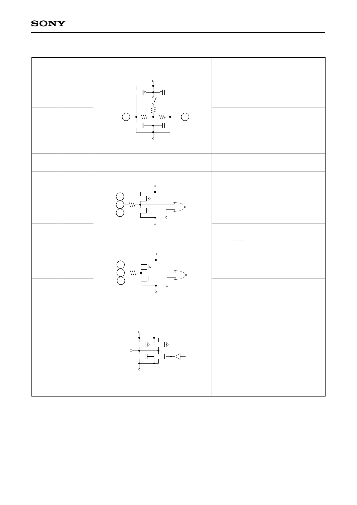
Pin Description
CXD2301Q
Pin No. Symbol
1VRB
23 VRT
2, 3, 7,
28, 31
AVSS
4 SEL
5CE
19 TEST
Equivalent circuit Description
AVDD
Reference voltage (bottom)
Connect to AVSS for normal use.
When another external voltage is input,
connect an external 0.1µF capacitor and
retain a 1.5V differential compared to the
top reference voltage.
Reference voltage (top)
By setting VRB to AVSS, outputs
23
TS
R
Rref
1
approximately 1.5V.
Connect only a 0.1µF external by-pass
capacitor for normal use.
AVSS
When another external voltage is input, it
must be 2.2V or lower.
Analog GND.
AVDD
4
5
19
DVSS
AVSS
Switches the input of the 3x amplifier.
When SEL is at Low level, VIN1 is selected.
When SEL is at High level, VIN2 is selected.
Standby function ON/OFF selector.
In standby state when High.
Fix to VSS for normal use.
6 CLE
18 CLK
20 CLP
8DVSS
9 to 16 D7 to D0
17 DVDD
20
18
AVDD
enabled.
When CLE = High: Clamp function is
When CLE = Low: Clamp functiion is
6
disabled, and only the normal A/D
converter function is enabled.
Clock input
CE
AVSS
Inputs the clamp pulse to Pin 20 (CLP).
Clamps the High interval signal voltage.
Digital GND.
D7 (MSB) to D0 (LSB) output
Outputs Low level in standby.
Di
In operation, the phase of D7 to D0
output is inverted against the phase of
ADIN.
5V or 3.3V
– 3 –
Page 4
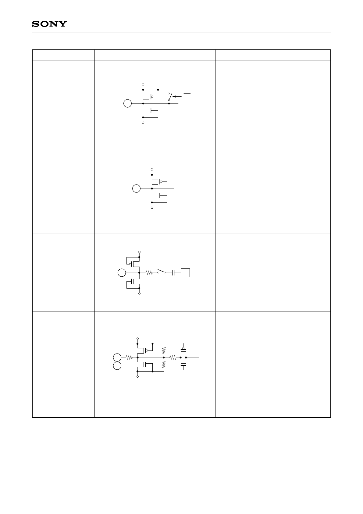
Pin No. Symbol Equivalent circuit Description
AVDD
CE
21 ADV
21
AVSS
Short Pins 21 and 22, and connect 0.1µF
external capacitor.
AVDD
CXD2301Q
22 ADV
24 VREF
25
27
VIN1
VIN2
22
AVSS
AVDD
24
AVSS
AVDD
200 R
25
27
AVSS
R11
R12
Clamp reference voltage input.
Clamps so that the reference voltage
and the clamp interval ADIN input signal
are equal.
The reference voltage is more than 0.5V.
Amplifier input pin.
Biased internally
at 1.9V (when AVDD = 5V) or
at 1.8V (when AVDD = 4.75V).
When in standby as well.
When SEL is at Low level, VIN1 is
selected for input;
When SEL is at High level, VIN2 is
selected for input.
26 AVDD
5V or 4.75V
– 4 –
Page 5
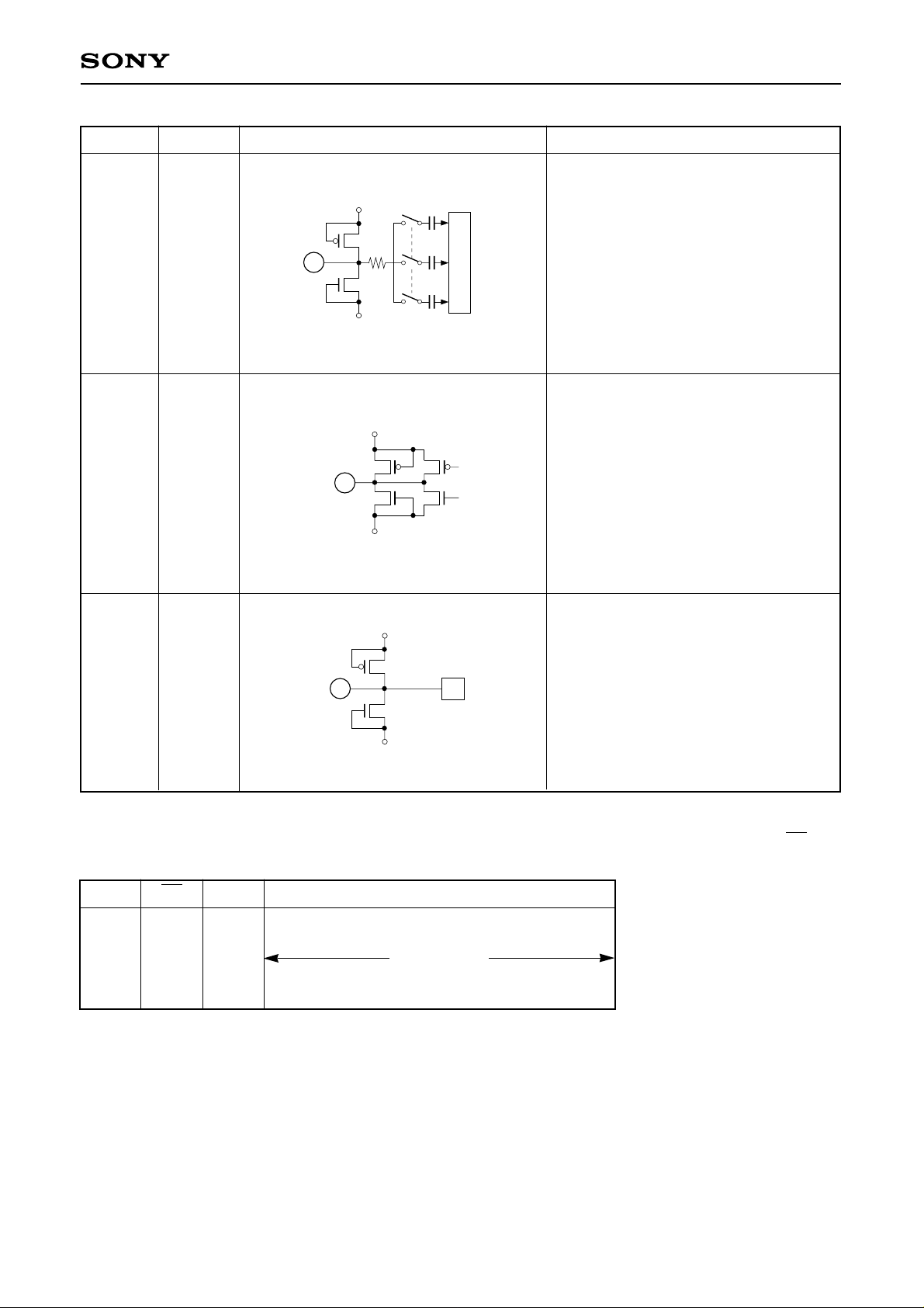
Pin No. Symbol Equivalent circuit Description
AVDD
CXD2301Q
29 ADIN
30 OPO
32
CCP
29
32
30
A/D converter block analog input.
AVSS
AVDD
Amplifier output.
The phase of this output is inverted
against the phase of VIN1, 2.
In standby mode, it becomes
high-impedance output condition.
AVSS
AVDD
Integrates the clamp control voltage.
The relationship between the CCP
voltage variation and the ADIN voltage
is positive phase.
AVSS
• The following table shows the status of the digital output pins when the TEST pin is used with the CE and
SEL pins.
TEST
L
L
H
H
H
CE
L
H
L
H
H
SEL
X
X
X
L
H
D1 D2 D3 D4 D5 D6 D7 D8
D1 D2 D3 D4 D5 D6 D7 D8
LLLLLLLL
TEST mode
HLHLHLHL
LHLHLHLH
– 5 –
Page 6
CXD2301Q
Digital Output
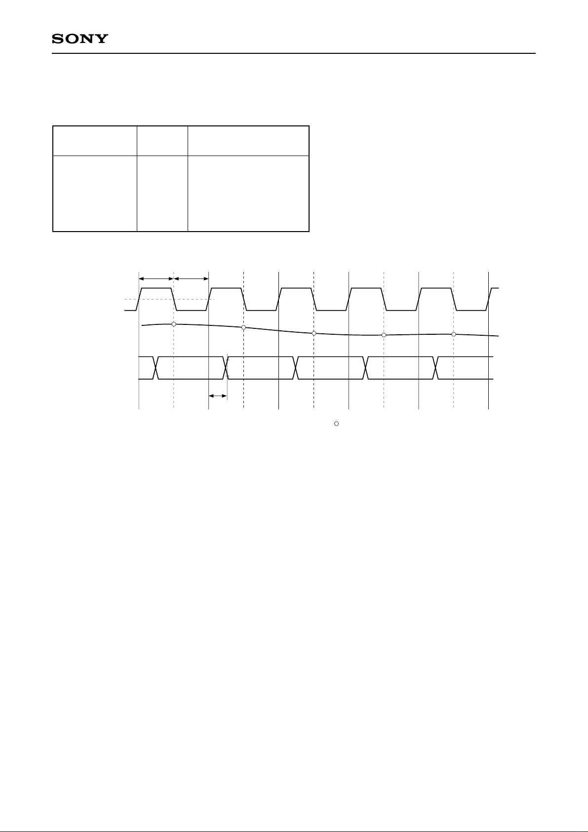
The following table shows the correlation between the ADIN input voltage and the digital output code.
Take notice that the phase of ADIN input signal voltage is inverted against the phase of the digital output.
ADIN
Input signal voltage
VRT
:
:
:
:
VRB
Clock 2V
ADIN input
Data output
Step
MSB LSB
0
:
127
128
:
255
TPW1 TPW0
N
N–3 N–2 N+1 N N–1
Digital output code
0 0 0 0 0 0 0 0
:
0 1 1 1 1 1 1 1
1 0 0 0 0 0 0 0
:
1 1 1 1 1 1 1 1
N+1
Td
N+2
N+3
N+4
Fig. 1. Timing Chart
: Indicates point at which input signal is sampled
– 6 –
Page 7
CXD2301Q
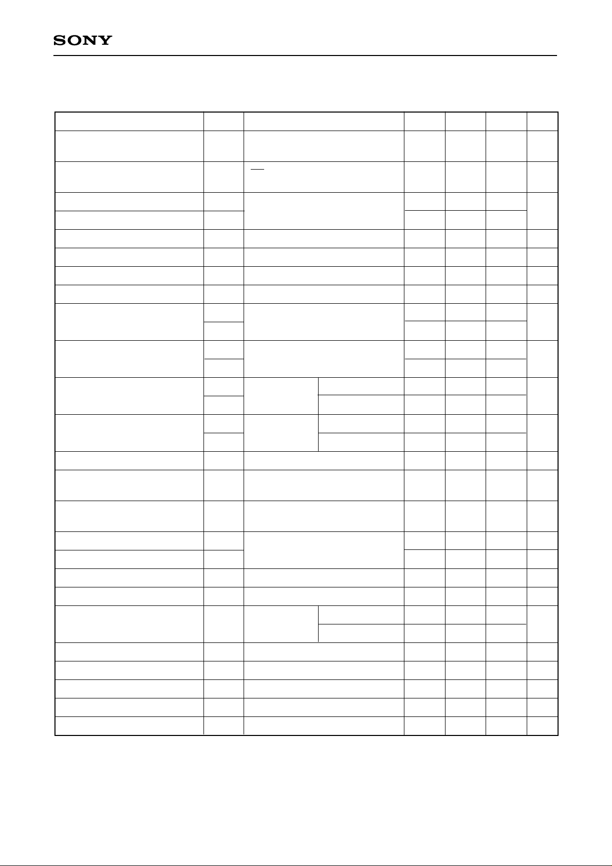
Electrical Characteristics
(1) When using a single power supply (Fc = 30MSPS, AVDD = DVDD = +5V, VRB = 0V, VRT = 1.5V, Ta = 25°C)
Item Symbol Conditions Min. Typ. Max. Unit
Supply current
Standby supply current
Max. conversion rate
Min. conversion rate
ADIN input band (at –1dB)
ADIN input capacitance
Reference resistance (VRT to VRB)
Self bias
Offset voltage
Digital input voltage
Digital input current
Digital output current
IAD +
IDD
ISTB
Fc max
Fc min
BW
CADIN
RREF
VRT
EOT
EOB
VIH
VIL
IIH
IIL
IOH
IOL
Fc = 35MSPS
NTSC ramp wave input
CE = DVDD
VIN = 0 to 1.5V
fIN = 1kHz ramp
VIN = 0.75V + 0.07Vrms
VRB = AVSS
VIH = VDD
DVDD = max.
VIL = 0V
VOH = VDD–0.5V
DVDD = min.
VOL = 0.4V
30
230
1.38
–40
+25
3.5
–1.1
3.7
27
130
20
8
330
1.52
–20
+45
–2.5
6.5
35
200
0.5
440
1.66
0
+65
0.5
5
5
mA
µA
MSPS
MHz
pF
Ω
V
mV
V
µA
mA
Output data delay
Integral nonlinearity error
Differential nonlinearity error
Differential gain error
Differential phase error
Aperture jitter
Sampling delay
Clamp offset voltage
Clamp pulse delay
Amplifier gain
VIN1 and VIN2 bias voltage
VIN1 and VIN2 input resistance
VIN1 and VIN2 input capacitance
TDL
EL
ED
DG
DP
taj
tsd
Eoc
tcpd
VBI1, 2
RI1, 2
CI1, 2
With TTL 1gate and 10pF load
Fc = 30MSPS
VIN = 0 to 1.5V
Fc = 30MSPS
VIN = 0 to 1.5V
NTSC 40IRE mod
ramp, Fc = 14.3MSPS
VADIN = DC,
PWS = 3µsec
VREF = 0.5V
VREF = 1.5V
DC to 15MHz
When open
7
0
–40
8.5
19
13
+0.5
±0.3
1
0.5
30
2
+20
–20
25
9.5
1.9
27
15
25
+1.3
±0.5
+40
0
10.5
35
ns
LSB
LSB
%
deg
ps
ns
mV
ns
dB
V
kΩ
pF
– 7 –
Page 8
CXD2301Q
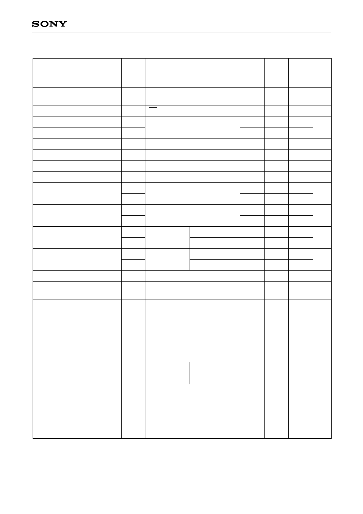
(2) When using a dual power supply (Fc = 30MSPS, AVDD = 4.75V, DVDD = 3.3V, VRB = 0V, VRT = 1.5V, Ta = 25°C)
Item Symbol Conditions Min. Typ. Max. Unit
Analog supply current
Digital supply current
Standby supply current
Max. conversion rate
Min. conversion rate
ADIN input band (at –1dB)
ADIN input capacitance
Reference resistance (VRT to VRB)
Self bias
Offset voltage
Digital input voltage
Digital input current
IAD
IDD
ISTB
Fc max
Fc min
BW
CADIN
RREF
VRT
EOT
EOB
VIH
VIL
IIH
IIL
Fc = 30MSPS
NTSC ramp wave input
Fc = 30MSPS
NTSC ramp wave input
CE = DVDD
VIN = 0 to 1.5V
fIN = 1kHz ramp
VIN = 0.75V + 0.07Vrms
VRB = AVSS
VIH = DVDD
DVDD = max.
VIL = 0V
30
230
1.44
–40
+25
2.5
24
1
130
20
8
330
1.52
–20
+45
32
2
200
0.5
440
1.6
0
+65
0.5
5
5
mA
mA
µA
MSPS
MHz
pF
Ω
V
mV
V
µA
Digital output current
Output data delay
Integral nonlinearity error
Differential nonlinearity error
Differential gain error
Differential phase error
Aperture jitter
Sampling delay
Clamp offset voltage
Clamp pulse delay
3x amplifier gain
VIN1 and VIN2 bias voltage
VIN1 and VIN2 input resistance
IOH
IOL
TDL
EL
ED
DG
DP
taj
tsd
Eoc
tcpd
VBI1, 2
RI1, 2
DVDD = min.
VOH = VDD–0.5V
VOL = 0.4V
With TTL 1gate and 10pF load
Fc = 30MSPS
VIN = 0 to 1.5V
Fc = 30MSPS
VIN = 0 to 1.5V
NTSC 40IRE mod
ramp, Fc = 14.3MSPS
VIN = DC,
PWS = 3µsec
VREF = 0.5V
VREF = 1.5V
DC to 15MHz
When open
–1.1
3.7
7
0
–40
8.5
19
–2.5
6.5
13
+0.5
±0.3
1
0.5
30
2
+20
–20
25
9.5
1.8
27
25
+1.3
±0.5
+40
0
10.5
35
mA
ns
LSB
LSB
%
deg
ps
ns
mV
ns
dB
V
kΩ
VIN1 and VIN2 input capacitance
CI1, 2
– 8 –
15
pF
Page 9
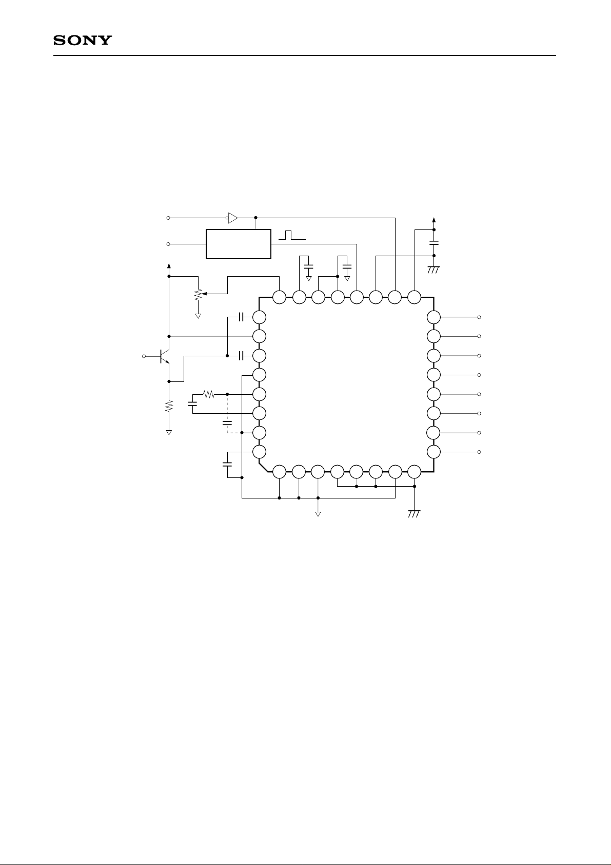
Application Circuit
(1) When using the internal amplifier
a) Clamp usage example (using self bias)
CXD2301Q
CLOCK IN
CLAMP PULSE IN
VIDEO IN
+4.75V
20k
0.1µ
LATCH *
75
10p
0.01µ
ACO4
VREF
0.1µ
0.1µ
CK
26
27
28
29
30
32
25
31
+3.3V
Q
23
24
1
2
0.1µ
22
3
21
4
0.1µ
20
19
18
17
6
5
7
0.1µ
16
15
14
13
12
11
10
9
8
D0
D1
D2
D3
D4
D5
D6
D7
GND (dig ita l)GND (analog)
∗
Although the ADC sampling clock latches the clamp pulse, it is not needed for basic clamp
operation. However, depending on the relationship between the sampling frequency and the
clamp pulse frequency, a small beat might be generated as V sag. The latch circuit is valid at
this time.
– 9 –
Page 10

b) Digital clamp usage example (using self bias)
CXD2301Q
VIDEO
IN1
VIDEO
IN2
CLOCK IN
+4.75V
0.1µ
75
ACO4
0.1µ
0.1µ
25
26
27
28
29
30
31
32
24
+3.3V
0.1µ
0.1µ
19
23
1
2
22
21
20
5
4
3
18
17
6
8
7
16
15
14
13
12
11
10
0.1µ
Subtracter,
Comparator,
etc.
9
Clamp Level
Setting data
DAC,
GND (dig ita l)GND (analog)
∗
The relationship between the CCP voltage (Pin 32) variation and the ADIN voltage variation is
PWM,
etc.
High impedance for all
information outside the
clamp interval
positive phase.
∗
∆ADIN/∆VCCP = 3.0 (fs = 30MSPS)
– 10 –
Page 11

c) When not using the clamp
CXD2301Q
CLOCK IN
VIDEO IN
+4.75V
0.1µ
0.1µ
75
10p
ACO4
0.1µ
0.1µ
25
26
27
28
29
30
31
32
23
24
1
GND (analog)
22
2
0.1µ
3
21
18
7
+3.3 V (d igit al)
0.1µ
17
16
15
14
13
12
11
10
9
8
GND (dig ita l)
D0
D1
D2
D3
D4
D5
D6
D7
0.1µ
19
20
6
5
4
+3.3 V (d igit al)
– 11 –
Page 12
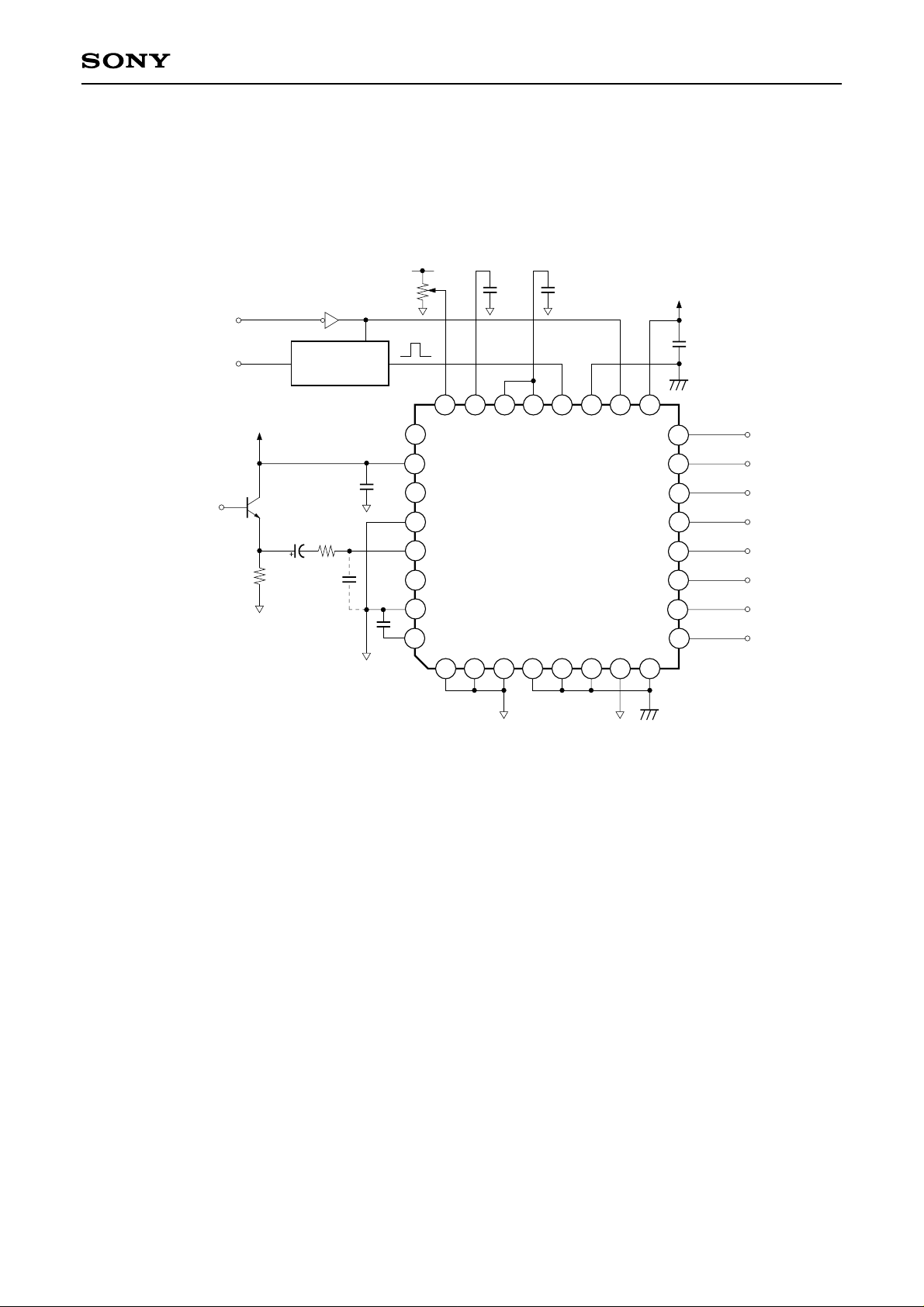
(2) When not using the internal amplifier
a) Clamp usage example
ACO4
CLOCK IN
CLAMP PULSE IN
LATCH *
+4.75V (analog)
CK
Q
+4.75V
25
20k
24
23
22
0.1µ
21
20
0.1µ
19
18
+3.3 V (d igit al)
17
16
CXD2301Q
0.1µ
D0
26
0.1µ
29
30
32
27
28
31
6
1
2
3
5
4
7
GND (dig ita l)GND (analog)
VIDEO IN #
75
10µ
10p
0.01µ
∗
Although the ADC sampling clock latches the clamp pulse, it is not needed for basic clamp
15
14
13
12
11
10
9
8
D1
D2
D3
D4
D5
D6
D7
operation. However, depending on the relationship between the sampling frequency and the
clamp pulse frequency, a small beat might be generated as V sag. The latch circuit is valid at
this time.
# Take care that the phase of ADIN input is inverted against the phase of the digital output,
because the use of the built-in inverting amplifier is standard. (Refer to “Digital Output” on page
6.)
– 12 –
Page 13
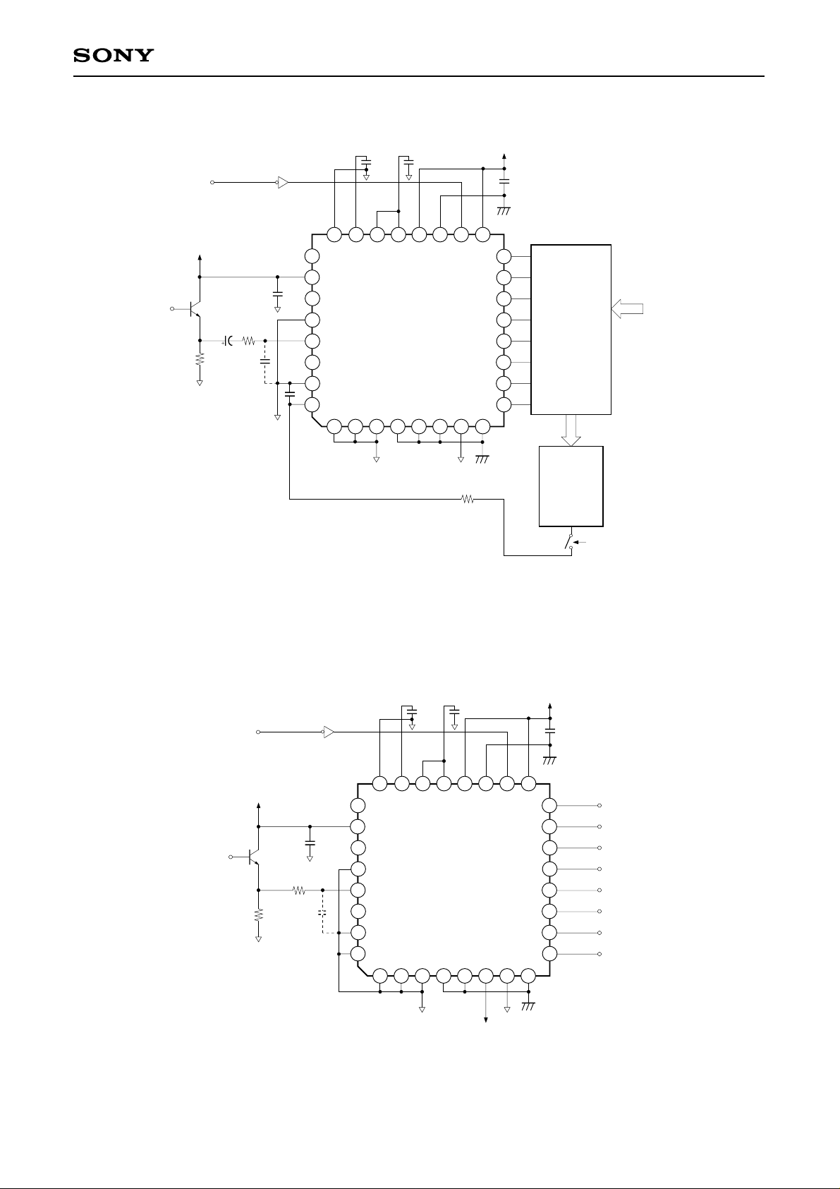
b) Digital clamp usage example
CXD2301Q
VIDEO IN #
CLOCK IN
+4.75V (analog)
10µ
75
10p
ACO4
0.01µ
0.1µ
18
7
{ 3.3V (digital)
0.1µ
17
16
15
14
13
12
11
10
9
8
Subtracter,
Comparator,
etc.
DAC,
PWM,
etc.
Clamp Level
Setting data
High impedance for all
information outside the
clamp interval
0.1µ
23
24
25
26
27
28
29
30
31
32
22
1
2
3
0.1µ
21
19
20
6
5
4
GND (d igital)GND (analog)
∗
The relationship between the CCP voltage (Pin 32) variation and the ADIN voltage variation is
positive phase.
∗
∆VADIN/∆VCCP = 3.0 (fs = 20MSPS)
c) When not using the clamp
CLOCK IN
+4.75V (analog)
VIDEO IN #
0.1µ
75
10p
ACO4
18
7
+3. 3V (digital)
0.1µ
17
16
15
14
13
12
11
10
9
8
D0
D1
D2
D3
D4
D5
D6
D7
0.1µ
0.1µ
23
22
24
25
26
27
28
29
30
31
32
1
2
3
19
21
20
6
5
4
GND (d igital)
GND (analog)
+3. 3V (digital)
# Take care that the phase of ADIN input is inverted against the phase of the digital output,
because the use of the built-in inverting amplifier is standard. (Refer to “Digital Output” on page
6.)
– 13 –
Page 14

Example of Representative Characteristics
CXD2301Q
–10
VDD=4.75V
VIN=150mVrms
–20
VIN1=GND
–30
–40
–50
Crosstalk [dB]
–60
–70
–80
1 5 10 50
fIN–Input frequency [MHz]
Input frequency of VIN2 vs.
Crosstalk V
IN2→VIN1
fIN=NTSC ramp wave
VIN=150mVrms
30
Current consumption [mA]
20
0.1 0.5 1
fs–Sampling frequency [MHz]
510
Sampling frequency vs. Current consumption
VDD=5V,
Input waveform is ramp wave
VIN=150mVrms
40
30
Current consumption [mA]
20
0.1 0.5 1 50
fIN–Input frequency [MHz]
510
Input frequency vs. Current consumption
– 14 –
Page 15
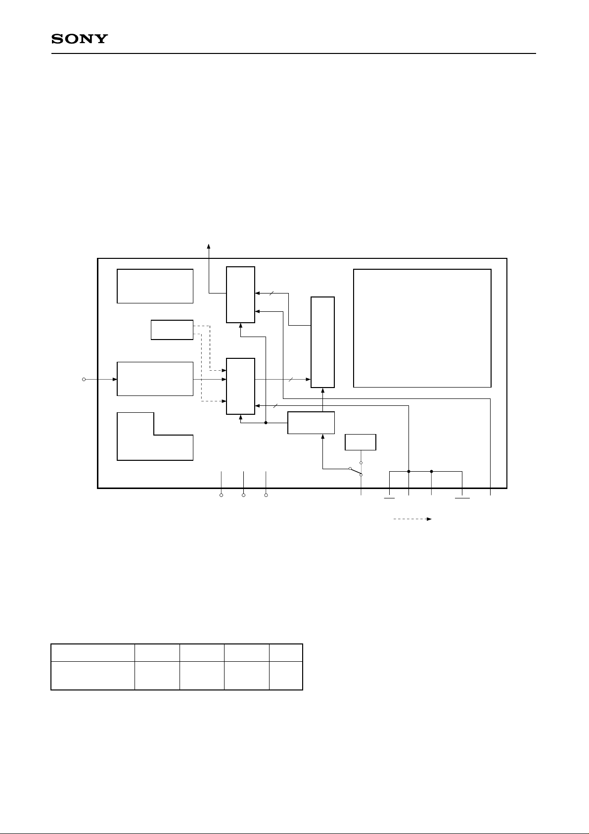
CXD2301Q
8bit ADC and DAC Evaluation Board
Evaluation boards are available for the high speed, low power consumption CMOS converters, CXD2301Q
(8-bit 30MHz A/D) and CXD1171M (8-bit 40MHz D/A).
The evaluation board is composed of a main board common to either type, to which is added sub board
D2301Q or sub board D1171M. The junction is made through a socket.
To the main board are mounted an input interface, clock buffer and latch. To each of the sub boards is
mounted CXD2301Q and CXD1171M respectively. Those IC's are mounted according to recommended print
patterns designed to provide maximum performance to the A/D and D/A converters.
Block Diagram
V OUT
V IN
ANALOG CIRCUIT
MOUNT PORTION
DAC
V REF
ANALOG INPUT
INTE RFACE
DAC
ANALOG CIRCUIT
MOUNT PORTION
SOCKET
SOCKET
8
DIGITA L CIRCUIT MO UNT
PORTION
DATA LATCH
8
4
CLOCK
BUFFE R
OSC
SW
–5V+5VGND
CLOCK OE SEL SYNC CLE BLK
Unnecessary at
self bias use
Characteristics
• Resolution 8bit
• Maximum conversion rate 30MHz
• Digital input level CMOS level
• Supply voltage ±5.0V (Single +5V power supply possible at self bias use)
Supply Voltage
Item
Min. Typ. Max. Unit
+5V
–5V
Clock Input
CMOS compatible
Pulse width TCW1 16ns (min)
TCW0 16ns (min)
165
20
mA
– 15 –
Page 16
Analog Output (CXD1171M) (RL > 10kΩ)
CXD2301Q
Item
Analog output
Min. Typ. Max. Unit
1.8 2.0 2.1 V
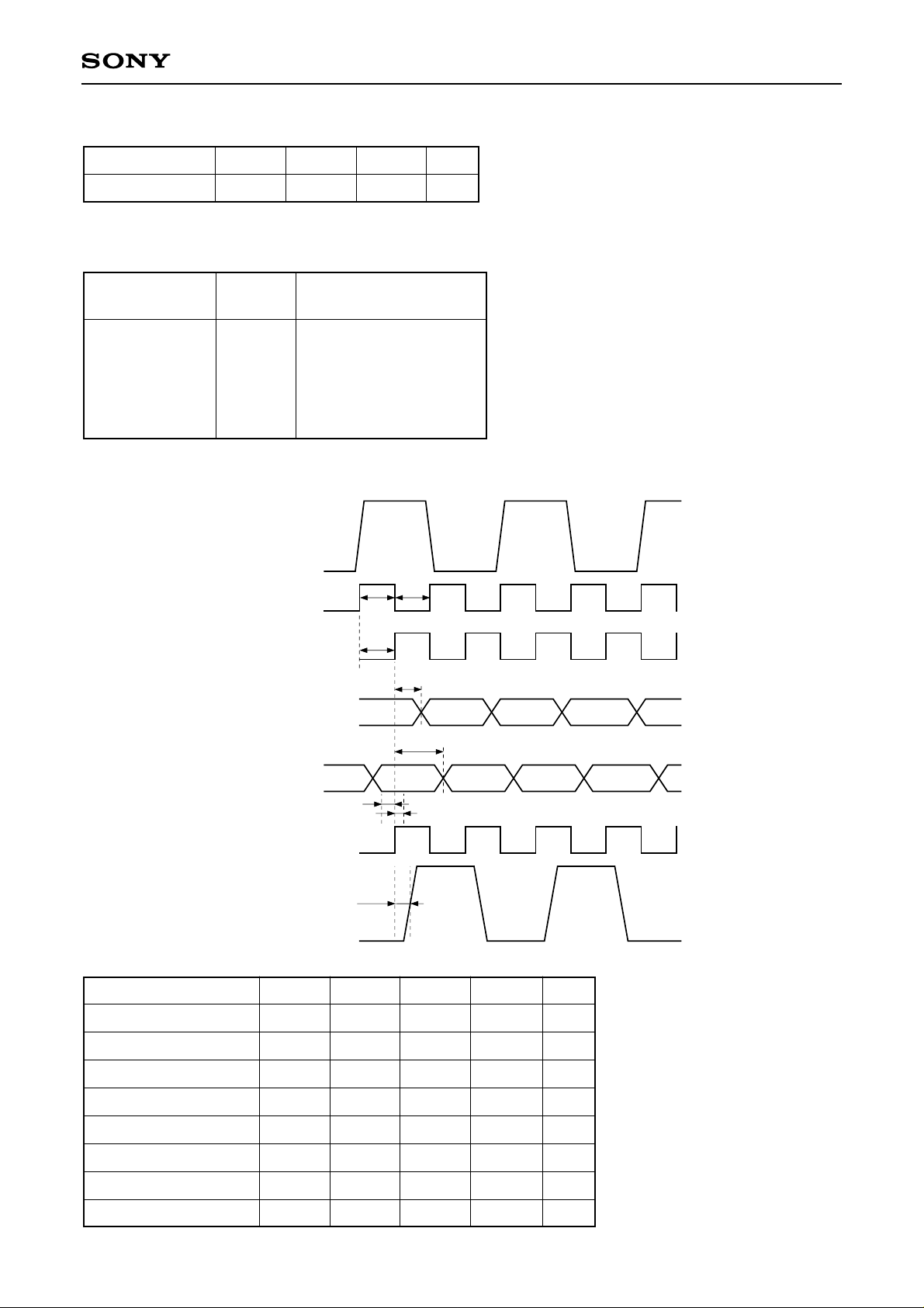
Output Format (CXD2301Q)
The table shows the output format of AD Converter
Analog input
voltage
VRT
:
:
:
:
VRB
Step
0
:
127
128
:
255
Digital output code
MSB LSB
0 0 0 0 0 0 0 0
:
0 1 1 1 1 1 1 1
1 0 0 0 0 0 0 0
:
1 1 1 1 1 1 1 1
Timing Chart
Analog input
External clock
TPW0
TPW1
Item
Clock High time
Clock Low time
Clock Delay
AD clock
AD output
Latch output
DA input
DA clock
DA output
Symbol Min. Typ. Unit
TPW1
TPW0
Tdc
tS
tPD(DA)
16
16
tPD(AD)
tDD
th
Max.
Tdc
24
ns
ns
ns
Data delay AD
Data delay (latch)
Settling time
Hold time
Data delay DA
tPD (AD)
tDD
tS
th
tPD (DA)
5
10
13
10
– 16 –
25
5
ns
ns
ns
ns
ns
Page 17

CXD2301Q
75
R10
47µ
SYNC INT
(R IN=75µ)
20k
OE
SEL
VR5
CLE
DVDD
14
DVSS
1
8
7
OUT
EXTERNAL CLO CK
INPUT
R9
75
OSC
OSC SWITCH
EXT/INT
BLK
SYNC
0.01µ
6
AVSSAVSS
23
C4
SS
DV
7
8
4
6
5
74HC0 4
9
11
10
OR
1
3
2
(INV BUFFER)
74S04
14
13
12
DVDD
DVDD
DVSS
4
5
VRBS
25
24
0.01
D0
VRB
26
1
3
2
SS
OE
DV
VREF
CLE
28
27
SW3
47µ
20k
VR3
0.01
DV
DD
AV
DD
GND
+5 V
–5V
SS
0.01µ
7
74S174
9
10
CLK DVSS
6
(LATCH)
11
4
5
13
12
1
3
2
14
16
15
DVDD
8
CLEAR
0.01µ
DV
CLK
8
7
9
10
4
6
5
13
11
12
1
3
2
74S174
(LATCH)
14
16
15
DVDD CLEAR
DVSS
8
7
9
11
10
12
SS
NC
DV
DVDD
NCNCAV
13
14
OUTPUT
GAIN
ADJUST
D7D6D5D4D3D2D1
BLK
CLK
SS
AVSS
IREF
VREF
16
15
17
18
R8
3.3k
(16R)
C5
0.1
20k
VR4
4
6
5
AVDD
AVDDIOIONCDV
21
19
20
R7
3
22
200
1
2
14
D0
SYNC
DD
SW1
PWNCNC
24
23
(R)
15
OUT
V
13
SEL
16
11
12
DD
CLK
DV
RT
V
17
18
SW2
8
7
9
10
D7D6D5D4D3D2D1
VRTS
AVDD
AVDD
VIN
21
19
C3
22
20
0.01
CMOS ADC/DAC Peripheral Circuit Board (Main Board)
Q2
DD
AV
VRT
ADJUST
VRB
ADJUST
VR2
R4
2k
510
R5
510
AVSS
Q1
R6
510
2k
VR1
75
R3
AVDD
C2 10µ
R2
AVSS
75
CLAMP
VOLTAGE
ADJUST
Q3
C1 470µ
C3
R1
100k
VIDEO INPUT
– 17 –
Page 18

CMOS ADC/DAC Peripheral Circuit Board (Sub Board)
C3
24
0.01µ
C2
0.1µ
23
22
21
CXD2301Q
1
2
4
3
CLP
NC
NC
NC
NC
AV
AVDD
VIN
AV
AVSS
NC
NC
V
REF
DD
SS
15
16
17
18
19
20
22
23
24
25
26
21
27
C4
0.1µ
C6
1µ
C5
1000p
25
26
27
28
29
30
31
32
20
CXD2301Q
NC
14
C1
19
18
17
0.1µ
16
15
14
13
12
11
10
9
6
5
8
7
13
12
10
11
NC
CLK
DD
DV
D7
D6
9
D5
8
D4
7
D3
6
D2
5
D1
4
D0
3
SS
DV
2
CLE
NC
NC
AV
AV
IREF
VREF
AVDD
AVDD
NC
SS
SS
IO
IO
28
15
16
17
13
14
18
19
21
22
20
23
C3
C2
13
14
18
19
15
16
17
20
21
22
23
CXD1171M
12
11
10
NC
1
NC
12
SS
DV
C4
9
8
7
6
5
4
3
2
11
10
CLK
BLK
9
D7
8
D6
7
D5
6
D4
5
D3
4
D2
3
D1
2
DV
DD
24
24
C1
– 18 –
1
D0
1
Page 19
List of Parts
resitance transistor
R1 100k Q1 2SC2785
R2 75Ω Q2 2SC2785
R3 75Ω Q3 2SC2785
R4 510Ω
R5 510Ω ic
R6 510Ω IC1 74S174
R7 R = 200 IC2 74S174
R8 18R ≈ 3.3k IC3 74S04
R9 75Ω
R10 75Ω oscillator
VR1 2k OSC
VR2 2k
VR3 20k others
VR4 20k connector BNC071
VR5 20k SW AT1D2M3
capacitance
C1 470µF/6.3V (chemical)
C2 10µF/16V (chemical)
C3 0.01µF
C4 0.01µF
C5 0.1µF
C6 0.1µF
C7 0.1µF
C8 0.1µF
C9 0.1µF
C10 0.1µF
C11 47µF/10V (chemical)
C12 47µF/10V (chemical)
C13 47µF/10V (chemical)
C14 0.1µF
CXD2301Q
Adjustment
1. Vref adjustment (VR1, VR2)
Adjustment of A/D converter reference voltage. VRB is adjusted through VR1 and VRT through VR2. When
self bias is used, there is no need for adjustment. Reference voltage is set through self bias at delivery.
2. Setting of clamp reference voltage (VR3)
Clamp reference voltage is set.
3. DAC output full scale adjustment (VR4)
Full scale voltage of D/A converter output is adjusted at the PCB shipment, the full scale voltage is adjusted
to approx. 2V.
4. Sync (clamp) pulse interface (VR5)
This adjustment enables interface with the signal generator and others at the PCB shipment, adjustment is
performed to obtain a threshold of approx. 2.5V to an H sync of 0 to 5V.
– 19 –
Page 20

CXD2301Q
5. OE, SEL, Sync, BLK, CLE, Sync INT
The following pins are set on the main board: Sync, CLE, Sync INT (CXD2301Q) and BLK (CXD1171M),
OE, SEL (not used). For the pins function, refer to the specifications. The difference between Sync pin and
Sync INT pin is that you input a pulse above 3.5Vp-p to Sync INT pin. The pulse threshold is set through
VR5. For input through Sync pin, pulse is input at TTL or CMOS level. In this case cut off the junction line
between Sync pin and Sync INT pin.
At the PCB shipment the main board pins are set as follows.
........
• OE
• SEL
• Sync
• CLE
• BLK
Low
......
Low
.....
Line junction with Sync INT pin
......
Low (Clamp function ON)
......
Low (Blanking OFF)
6. Clamp pulse input method
The clamp pulse is directly input to CXD2301Q as show in Application Circuit examples (1) and (2). Use the
direct input that is set at the PCB shipment.
Points on the PCB Pattern Layout
1. Set the layout not to have Digital current flow into Analog GND (Part 1). (For 1, see P.17 Component side
diagram.)
2. At CXD2301Q sub board, C2 and C3 capacitors serve the important role of bringing out CXD2301Q's full
performance.
These are over 0.1µF (ceramic) capacitors with good high frequency characteristics. Layout as close to the
IC as possible.
3. Analog GND (AVSS) and Digital GND (DVSS) are on a common voltage and power source. Keeping ADC's
DVSS (Part 2) as close as possible to the voltage supply source will provide better results. That is, a layout
where ADC is close to the voltage supply source, is recommended. (For 2, see P.17 Component side
diagram.)
4. ADC samples analog signals at the clock falling edge point. Accordingly clocks supplied to ADC should not
have any jitter.
5. The PCB layout shows ADC and DAC's Analog GND independently from the voltage supply source. The
layout aims at providing an independent evaluation of ADC and DAC, as much as possible. On the actual
board, common use will not cause any problems.
– 20 –
Page 21

CXD2301Q
Notes on Operation
1. Reference voltage
By shorting VRT and VRTS, VRB and VRBS, CXD2301 has the self bias function that generates VRT = about
2.6V and VRB = about 0.5V. On the PCB, either self bias or the external reference voltage can be selected
depending on the junction method of the jumper line. At shipment from the factory, reference voltage is
provided in self bias. Also, to provide external reference voltage, adjust the dynamic range (VRT – VRB) to
above 1.8Vp-p.
2. Clock input
There are 2 modes for the PCB clock input.
1) Provided from the external signal generator (External clock)
2) Using the crystal oscillator (built-in clock driver). (Internal clock)
The 2 modes are selected using the switch on the PCB.
3. The 2 Latch IC's (74S174) are not absolutely necessary for the evaluation of ADC and DAC. That is,
operation will still be normal if ADC output data is directly input to DAC input. However, as ADC output data
is hardly ever D/A converted without executing Digital signal processing, it was mounted to indicate an
example layout of Digital signal processing IC. When the ADC output data is used, use the output of the
latch IC.
4. When clamp is not used
Turning CLE to H will set OFF the clamp function. In this case, the DC element is cut off by means of C2 on
the main board and DC voltage on the ADC side of C2 turns to about (VRT + VRB). To transfer DC elements
of input signals, short C2. At that time, it is necessary to bias input signals, but keeping R2 open, Q3 can
also be used as buffer. Use the open space for the bias circuit.
5. Clamp pulse latch
On the evaluation board, the clamp pulse is latched with ADC sampling CLK and then input to the CLP pin.
This is to minimize Vsag due the synchronizing of noise and clamp pulse beat elements with GND sampling
clock around ADC. If there are no problems with Vsag, latch is not necessary.
6. Peripheral through hole
There is a group of through holes on the Analog input, output and Logic. These are to be used when
mounting additional circuits to the PCB. Use when necessary.
The connector hole on DAC part is used to mount the test chassis and the mount jack.
– 21 –
Page 22
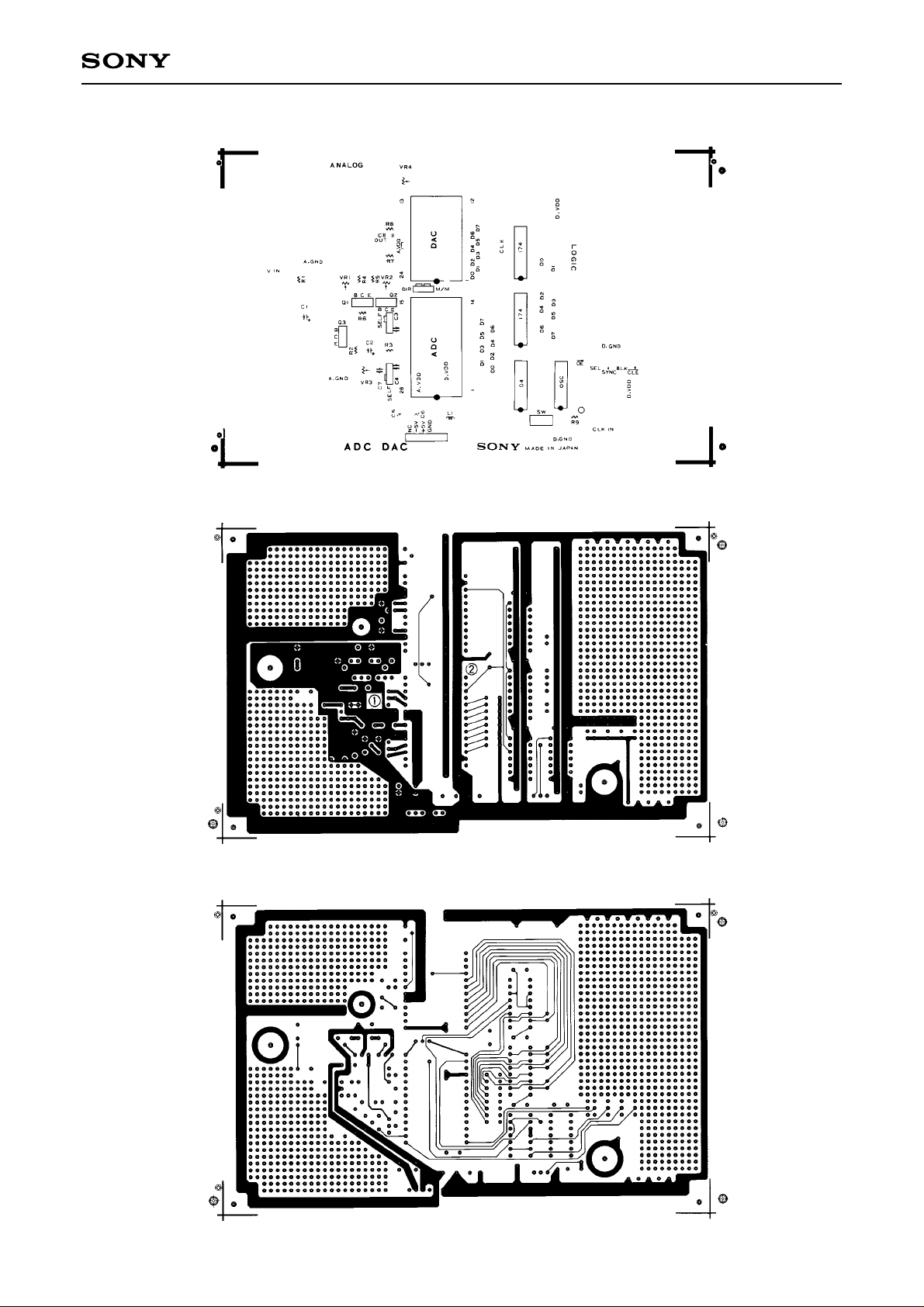
Silk Side
Component Side
CXD2301Q
Soldering Side (Diagram seen from the component side)
– 22 –
Page 23
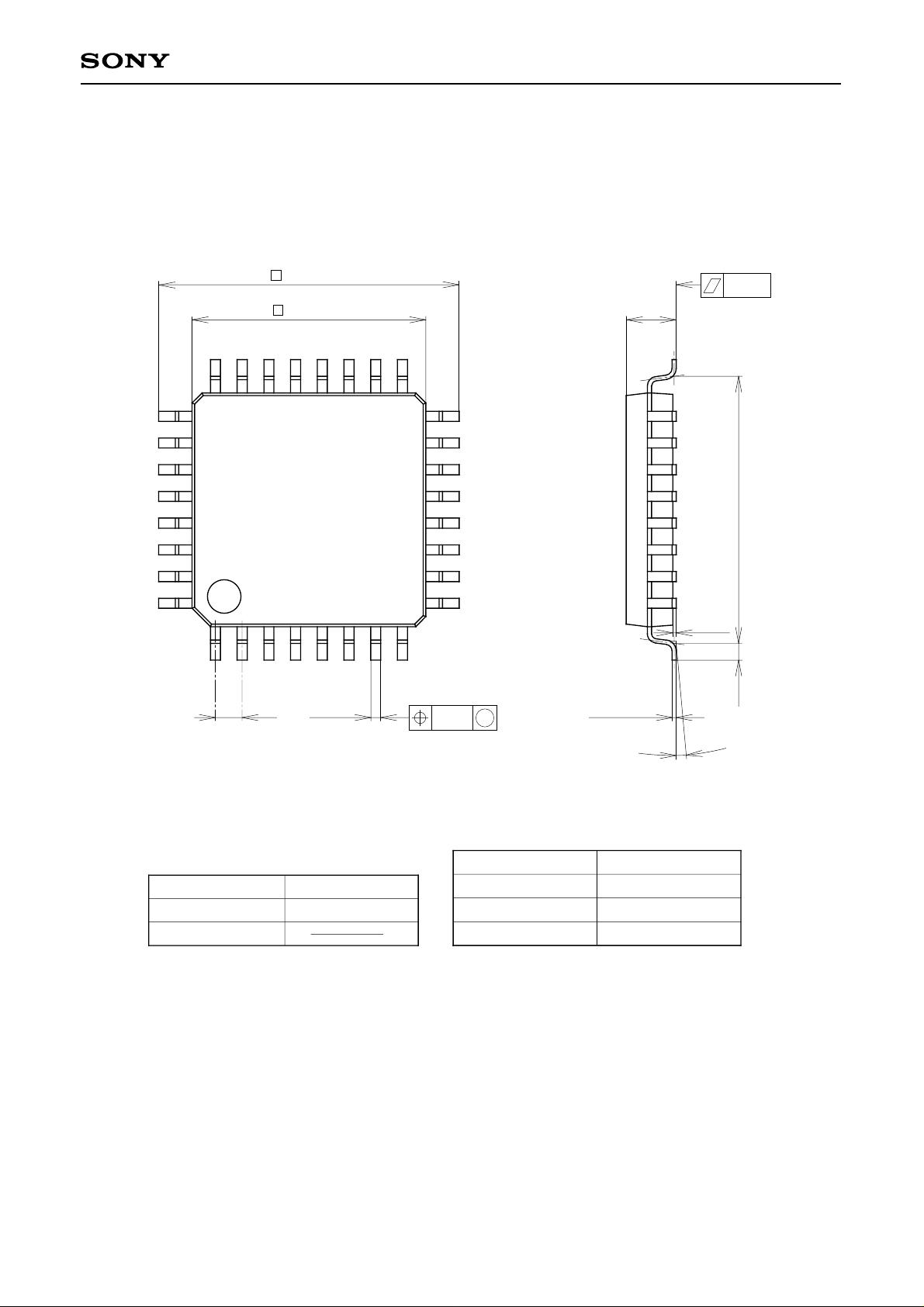
Package Outline Unit: mm
CXD2301Q
32PIN QFP (PLASTIC)
25
32
9.0 ± 0.2
+ 0.3
7.0 – 0.1
+ 0.35
1.5 – 0.15
0.1
1724
16
(8.0)
9
+ 0.2
0.1 – 0.1
1
0.8 0.3 – 0.1
+ 0.15
8
± 0.12
+ 0.1
M
0.127 – 0.05
0.50
0° to 10°
SONY CODE
EIAJ CODE
JEDEC CODE
QFP-32P-L01
∗QFP032-P-0707-A
PACKAGE MATERIAL
LEAD TREATMENT
LEAD MATERIAL
PACKAGE WEIGHT
– 23 –
EPOXY RESIN
SOLDER PLATING
42 ALLOY
0.2g
 Loading...