

Page 1
Description
The CXD2073S is an adaptive comb filter compatible
with NTSC system, and provide high-precision Y/C
separation with a single chip.
Features
• Y/C separation by adaptive processing
• Horizontal aperture compensation circuit
• 8-bit A/D converter (1 channel)
• 8-bit D/A converter (2 channels)
• One 1H delay line
• Clamp circuit
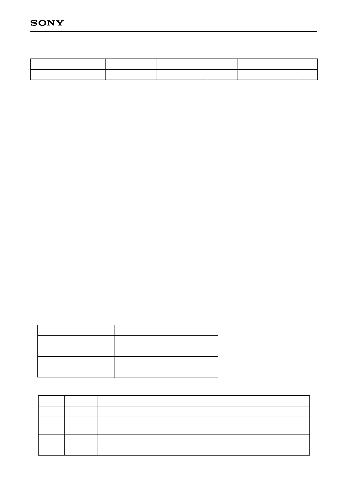
Absolute Maximum Ratings (Ta = 25°C, VSS = 0V)
• Supply voltage DVDD VSS – 0.5 to +7.0 V
DAVD VSS – 0.5 to +7.0 V
ADVD VSS – 0.5 to +7.0 V
PLVD VSS – 0.5 to +7.0 V
• Input voltage VI VSS – 0.5 to VDD +0.5 V
• Output voltage VO VSS – 0.5 to VDD +0.5 V
• Operating temperature
Topr –20 to +75 °C
• Storage temperature
Tstg –55 to +150 °C
Recommended Operating Conditions
• Supply voltage DVDD 5.0 ± 0.25 V
DAVD 5.0 ±0.25 V
ADVD 5.0 ±0.25 V
PLVD 5.0 ± 0.25 V
• Operating temperature
Topr –20 to +75 °C
Structure
Silicon gate CMOS IC
Applications
Y/C separation for color TVs and VCRs
– 1 –
CXD2073S
E97412B86-PS
Digital Comb Filter (NTSC)
Sony reserves the right to change products and specifications without prior notice. This information does not convey any license by
any implication or otherwise under any patents or other right. Application circuits shown, if any, are typical examples illustrating the
operation of the devices. Sony cannot assume responsibility for any problems arising out of the use of these circuits.
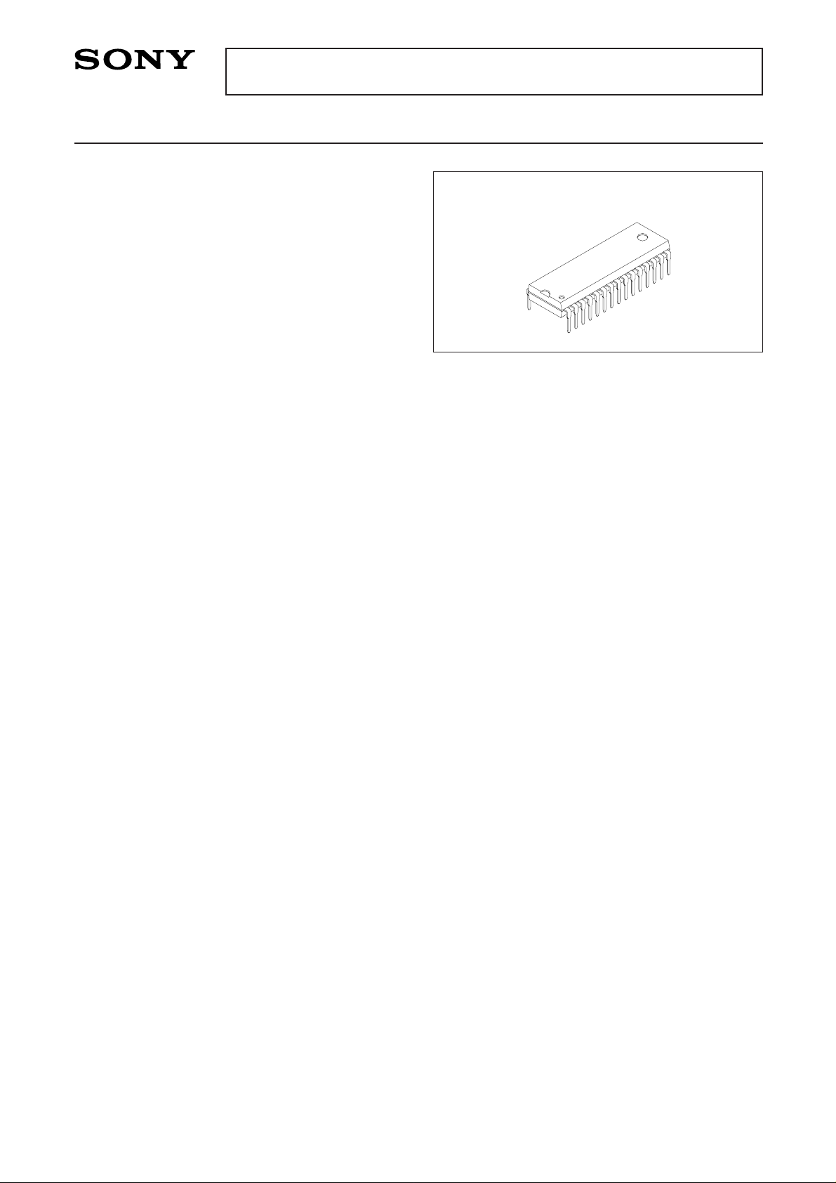
30 pin SDIP (Plastic)
For the availability of this product, please contact the sales office.
Page 2
– 2 –
CXD2073S
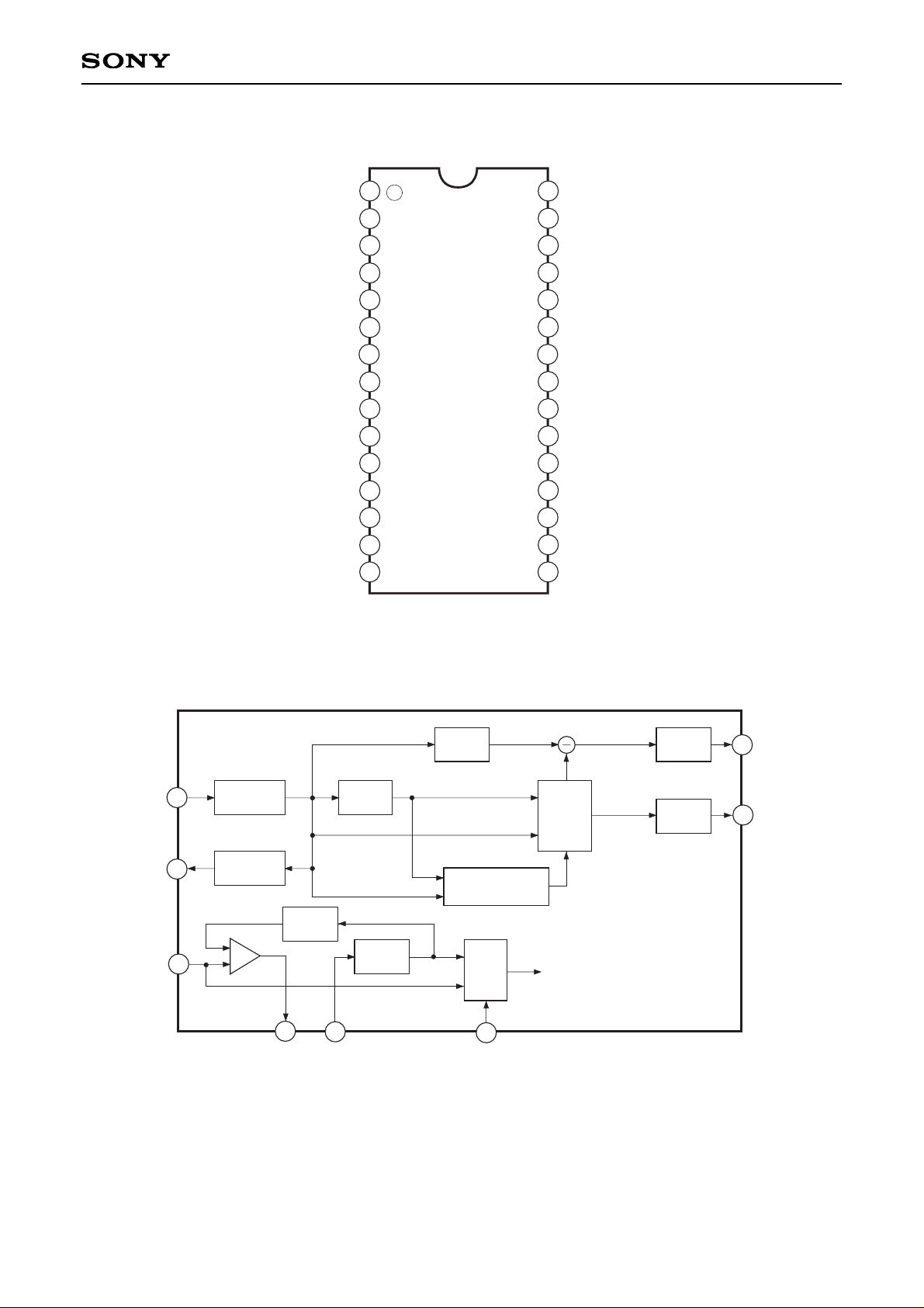
Pin Configuration (Top View)
Block Diagram
1
2
3
4
5
6
7
8
9
10
11
12
13
14
15
16
17
18
19
20
21
22
23
24
25
26
27
28
29
30
VCV
CPO
CKSL
FIN
TST1
TST2
DV
SS
DVDD
DVDD
DVSS
TST3
APCN
MOD1
MOD2
INIT
PLVD
PLVS
CLPEN
CLPO
ADIN
ADVS
ADVD
ACO
DAVD
AYO
DAVS
VRF
VG
VB
IRF
AYO
ACO
CKSL
VCV
CPO
FIN
CLPO
ADIN
A/D 1H
Clamp
DL D/A
D/A
1/4
VCO
SEL
Logic Operation
Block
Chroma
Output
Block
Internal clock
4
5
8
10
27
28
29
30
Page 3
– 3 –
CXD2073S
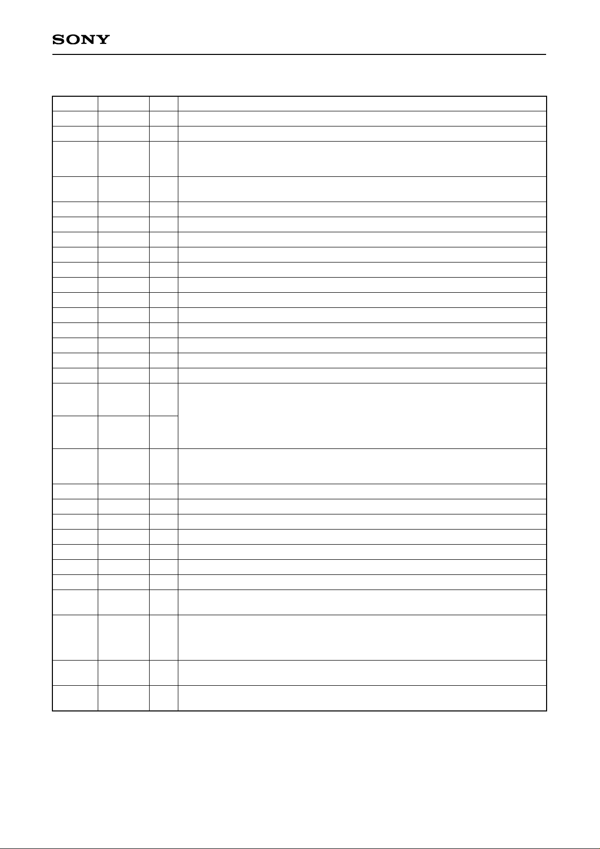
Pin Description
Pin No.
1
2
3
4
5
6
7
8
9
10
11
12
13
14
15
16
19
20
21
22
23
24
25
26
27
28
29
30
PLVD
PLVS
CLPEN
CLPO
ADIN
ADVS
ADVD
ACO
DAVD
AYO
DAVS
VRF
VG
VB
IRF
INIT
APCN
TST3
DVSS
DVDD
DVDD
DVSS
TST2
TST1
FIN
CKSL
CPO
VCV
—
—
I
O
I
—
—
O
—
O
—
I
O
O
O
I
I
O
—
—
—
—
O
I
I
I
O
I
Analog power supply for PLL (+5V)
Analog ground for PLL
Clamp enable
L: Clamp function is enabled. Set to L when the internal clamp is used.
H: Clamp function is disabled. Set to H when the internal clamp is not used.
Connect to ADIN when clamp circuit is used.
Leave this pin open when clamp circuit is not used.
Comb filter analog input (A/D converter input)
Analog ground for A/D converter
Analog power supply for A/D converter (+5V)
Analog chroma signal output
Analog power supply for D/A converter (+5V)
Analog luminance signal output
Analog ground for D/A converter
D/A converter reference voltage setting. Sets the full-scale value for D/A converter.
Connect to DAVD via a capacitor of approximately 0.1µF.
Connect to DAVS via a capacitor of approximately 0.1µF.
Connect a resistor of 16 times (16R) that of the output resistor "R" of AYO pin.
Test. Normally, fix to Low.
Y/C separation status setting pins
MOD2 MOD1
L L Adaptive processing mode
L H BPF separation fixed mode
H L Y through mode
H H Simple comb mode
Aperture compensation switching
L: Aperture compensation OFF
H: Aperture compensation ON
Test. Normally, leave this pin open.
Digital ground
Digital power supply (+5V)
Digital power supply (+5V)
Digital ground
Test. Normally, leave this pin open.
Test. Normally, fix to Low.
Clock input. Input burst-locked clock. Input fsc when the PLL is used. Input 4fsc
when the PLL is not used.
PLL control.
L: When the PLL is not used. The 4fsc clock input to FIN is supplied internally.
H:When the PLL is used. The 4fsc clock from VCO oscillation output is
supplied internally.
Phase comparison output for the internal PLL. Leave open when the PLL is not
used.
VCO oscillation control voltage input for the internal PLL. Connect to PLVS when
the PLL is not used.
Symbol I/O Description
17 MOD2 I
18 MOD1 I
Page 4
– 4 –
CXD2073S
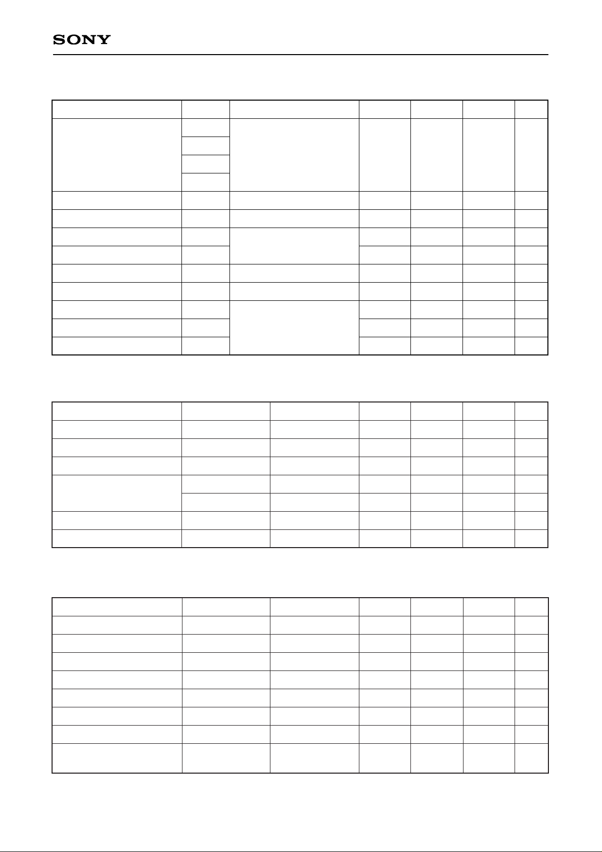
Electrical Characteristics (VDD = 5 ± 0.25V, VSS = 0V, Ta = –20 to +75°C)
Symbol
DVDD
ADVD
DAVD
PLVD
Topr
IDD
VIH
VIL
VOH
VOL
LVth
VIN
RFB
Conditions
—
—
Clock 14MHz
IOH = –2mA (Pin 20 and 25)
IOL = 4mA (Pin 20 and 25)
FIN (Pin 27)
Min.
4.75
–20
—
VDD × 0.7
VSS
VDD – 0.8
VSS
—
0.5
250k
Typ.
5.0
—
55
—
—
—
—
VDD/2
—
1M
Max.
5.25
+75
80
VDD
VDD × 0.3
VDD
0.4
—
VDD
2.5M
Unit
V
°C
mA
V
V
V
V
V
Vp-p
Ω
Item
Supply voltage
Operating temperature
Supply current
High level input voltage
Low level input voltage
High level output voltage
Low level output voltage
Logical Vth
Input voltage
Feedback resistor
A/D Converter Characteristics (VDD = 5V, Ta = 25°C, f = 10MHz)
Symbol
n
fmax
BW
BOTTOM
TOP – BOTTOM
ED
EL
Conditions
–3dB
Min.
—
14.3
—
0.48
1.96
–1.0
–3.0
Typ.
8
—
18
0.52
2.08
—
—
Max.
—
—
—
0.56
2.22
+1.0
+3.0
Unit
bit
MSPS
MHz
V
V
LSB
LSB
Item
Resolution
Max. conversion speed
Analog input band width
Input bias
Differential linearity error
Integral linearity error
D/A Converter Characteristics (VDD = 5V, VRF = 2V, IRF = 3.3kΩ, R = 200Ω, Ta = 25°C, f = 10MHz)
Symbol
n
fmax
ED
EL
VFS
IFS
VOS
VOC
Conditions
—
—
—
—
—
—
—
Min.
—
14.3
–0.8
–2.0
1.805
—
—
1.8
Typ.
8
—
—
—
1.90
9.5
—
—
Max.
—
—
+0.8
+2.0
1.995
15
1.0
2.1
Unit
bit
MSPS
LSB
LSB
V
mA
mV
V
Item
Resolution
Max. conversion speed
Differential linearity error
Integral linearity error
Output full-scale voltage
Output full-scale current
Output offset voltage
Precision guaranteed
output voltage range
CMOS level
(Pin 3, 16 to 19, 26, 28)
Page 5
– 5 –
CXD2073S
Clamp (VDD = 5V, Ta = 25°C, f = 10MHz)
Symbol
CLV
Conditions Min.
—
Typ.
0.67
Max.
—
Unit
V
Item
Clamp level
∗1
MOD1 (Pin 18)
L
L
H
H
MOD2 (Pin 17)
L
H
L
H
Modes
Adaptive processing mode
Y through mode
BPF mode
Simple comb mode
∗1
Sync tip clamp
Description of Functions
• Horizontal aperture compensation
Compensates aperture degradation accompanied by D/A conversion.
This compensation is effective for the following modes; adaptive processing, Y through, and simple comb
modes.
• Switching of Y/C separation modes
The following four modes can be set; however, the adaptive processing mode or Y through mode is normally
used.
(1) Adaptive processing mode
This mode detects interline correlation, switches between comb filter processing and BPF processing,
and operates Y/C separation.
(2) Y through mode
The composite video signal input from ADIN (Pin 5) is A/D converted. It is also D/A converted, and then
output from AYO (Pin 10).
At this time, the output of ACO (Pin 8) is the same output as that of adaptive processing mode.
(3) BPF mode
C signal is generated by passing composite video signal through BPF.
Y output is a signal in which the C signal generated is subtracted from input composite video signal.
(4) Simple comb mode
Y/C separation is operated by the comb filter processing forcibly.
• Selection Pin Setting Table
H
Internal clamp not used
See the table above.
Horizontal aperture compensation ON
Internal 4-multiple PLL used
L
Internal clamp used
Horizontal aperture compensation OFF
Internal 4-multiple PLL not used
Pin No. Symbol
3
17
18
19
28
CLPEN
MOD2
MOD1
APCN
CKSL
Page 6

– 6 –
CXD2073S
Application Circuit for D/A Converter
9
DAVD
11
DAVS
8
10
12
13
14
15
: analog power supply 5V : analog ground
AYO
VRF
IRF
ACO
VG
VB
0.1µ
0.1µ
3.3k
(R')
200
(R)
C OUT
Y OUT
200
(R)
0.1µ
2k
3k
0.1µ10µ
• Method of selecting output resistance
The CXD2073S has a built-in current output-type D/A converter. To obtain the output voltages, connect
resistors to AYO and ACO pins.
VFS = IFS × R
Here, VFS is output full-scale voltage, IFS is output full-scale current, and R is the output resistance
connected to each IO.
In addition, connect a resistance of 16 times the output resistor to the reference current pin IRF. In the case
where the value comes to be impractical, use a value of resistance as close to the value calculated as
possible. At that time,
VFS = VRF × 16 × R/R'.
R is the output resistance connected to each IO, R' is the resistance connected to IRF, and VRF is the VRF
pin voltage. Power consumption can be reduced by using higher resistance values, but then glitch energy
and data settling time increase contrastingly. Select optimum resistance values according to the system
applications.
In case of the circuit above, VFS = 2 [V] × 16 × 0.2k/3.3k ≈ 1.93 [V], IFS = 1.93/0.2k ≈ 9.65 [mA].
Page 7
– 7 –
CXD2073S
Notes on Operation
• Power supply, ground
Separate the analog and digital systems around the device to reduce noise effect. Both analog and digital
VDD are respectively bypassed to VSS as close to these VDD and VSS pins as possible through ceramic
capacitors of approximately 0.1µF.
Also, layout the power supply and ground pattern of the board substrate as wide as possible to lower
impedance.
• Clock
Use the burst-locked clock. Separate the clock line on the board substrate as far as possible from analogrelated pins, analog power supply, and analog ground.
• ADIN (analog input signal)
(1) Low impedance drive
The input signal to ADIN (Pin 5) should be driven at the low impedance and its wiring should be as short
as possible.
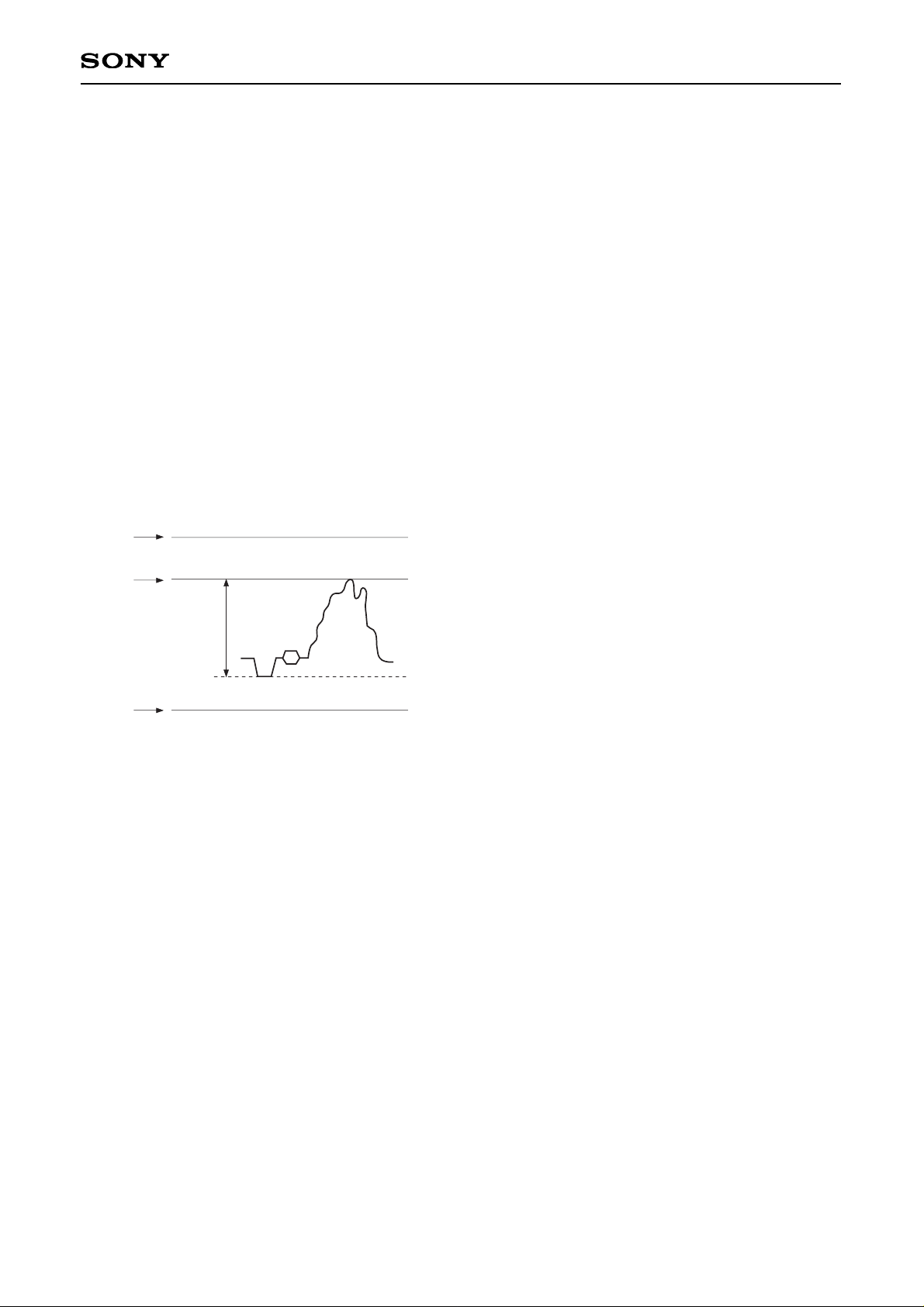
(2) Input level
Set the input signal peak-to-peak value VPP to 1.75V or less. Additionally, VPP is recommended to be
1.3V or more since the A/D converter input dynamic range should be made as large as possible.
VPP
2.60V (Reference top voltage typical value for internal A/D converter)
0.67V (Sync tip clamp level)
0.52V (Reference bottom voltage typical value for internal A/D converter)
C
B
A
The DC level at the ADIN pin is as shown in the diagram above when the internal sync tip clamp is used.
Labeling the internal D/A converter AYO output full-scale voltage as VFS, the correspondence between
the ADIN pin voltage and AYO output pin voltage (DC level) is as follows;
DC voltage at point A → 0 [V]
DC voltage at point B → AYO maximum output voltage [V]
DC voltage at point C → VFS [V]
The VFS is the AYO output voltage generated when the voltage equivalent to the point C is input.
• Internal delay
The delay from the internal A/D converter to the D/A converter output is 21.5 clocks + αns (α: D/A converter
analog output delay = approximately 20ns).
The 21.5 clocks are the sum of the clocks shown below;
A/D converter: 3.5 clocks (“0.5” is for fetching the data at the fall of the clock.)
Internal logic : 17 clocks
D/A converter: 1 clock
Page 8

– 8 –
CXD2073S
1
2
3
4
5
6
7
8
9
10
11
12
13
14
15
16
17
18
19
20
21
22
23
24
25
26
27
28
29
30
VCV
CPO
CKSL
FIN
TST1
TST2
DV
SS
DV
DD
DV
DD
DV
SS
TST3
APCN
MOD1
MOD2
INIT
PLVD
PLVS
CLPEN
CLPO
ADIN
ADVS
ADVD
ACO
DAVD
AYO
DAVS
VRF
VG
VB
IRF
0.1µ 0.1µ 0.1µ
0.1µ
3.3k
0.1µ
10µ
200200
5k
A5VA5VA5VA5V
H LH LH L
H L
D5V
0.1µ 0.1µ
0.001µ
Burst-locked
Clock
Clock
Generator
X'tal
3.58MHz
56k
560
0.022µ
A5V
L H
LPF
Y output
LPF
C output
LPF
10µ
Composite
video input
analog power supply (5V)
analog ground
digital power supply (5V)
digital ground
H: CMOS High level
L: CMOS Low level
Application circuits shown are typical examples illustrating the operation of the devices. Sony cannot assume responsibility for
any problems arising out of the use of these circuits or for any infringement of third party patent and other right due to same.
Application Circuit
(1) When the fsc clock is used
Recommended LPF: TH327LSJS-2513LCAS (TOKO)
(–3dB at 8MHz)
Page 9

– 9 –
CXD2073S
1
2
3
4
5
6
7
8
9
10
11
12
13
14
15
16
17
18
19
20
21
22
23
24
25
26
27
28
29
30
VCV
CPO
CKSL
FIN
TST1
TST2
DV
SS
DV
DD
DV
DD
DV
SS
TST3
APCN
MOD1
MOD2
INIT
PLVD
PLVS
CLPEN
CLPO
ADIN
ADVS
ADVD
ACO
DAVD
AYO
DAVS
VRF
VG
VB
IRF
0.1µ 0.1µ 0.1µ
0.1µ
3.3k
0.1µ
10µ
200200
5k
A5VA5VA5V
H LH LH L
H L
D5V
0.1µ 0.1µ
0.001µ
Burst-locked
Clock
Clock
Generator
X'tal
14.3MHz
L H
LPF
Y output
LPF
C output
LPF
10µ
Composite
video input
analog power supply (5V)
analog ground
digital power supply (5V)
digital ground
H: CMOS High level
L: CMOS Low level
Application circuits shown are typical examples illustrating the operation of the devices. Sony cannot assume responsibility for
any problems arising out of the use of these circuits or for any infringement of third party patent and other right due to same.
(2) When the 4fsc clock is used
Recommended LPF: TH327LSJS-2513LCAS (TOKO)
(–3dB at 8MHz)
Page 10
– 10 –
CXD2073S
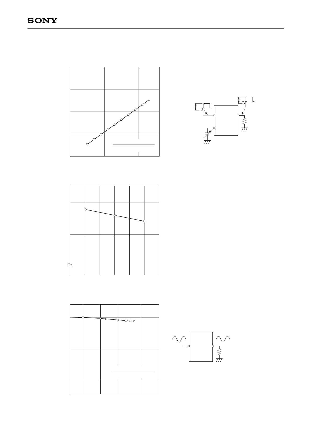
Example of Representative Characteristics
CXD2073S
AYOADIN
Input
1
VRF [V]
Analog I/O amplitude ratio vs. VRF pin voltage
Analog I/O amplitude ratio
0.5
1.0
1.5
2
25
Ta – Ambient temperature [°C]
Output full-scale voltage vs. Ambient temperature
VFS – Output full-scale voltage [V]
1.90
1.95
0
0.5
Frequency [MHz]
AYO (Y output) frequency response
Gain ratio [dB]
–1
0
–2
Input signal peak-to-peak voltage ≤ 1.75V
50 75–25 0
1 2 5
Gain for f = f [MHz]
Gain for f = 0.5 [MHz]
D/A output amplitude
A/D input amplitude
CXD2073S
AYOADIN
Input
VRF
Input amplitude
Output amplitude
R
200Ω
R
200Ω
V
DD = 5V
VRF = 2V
IRF = 3.3kΩ
R = 200Ω
Page 11
– 11 –
CXD2073S
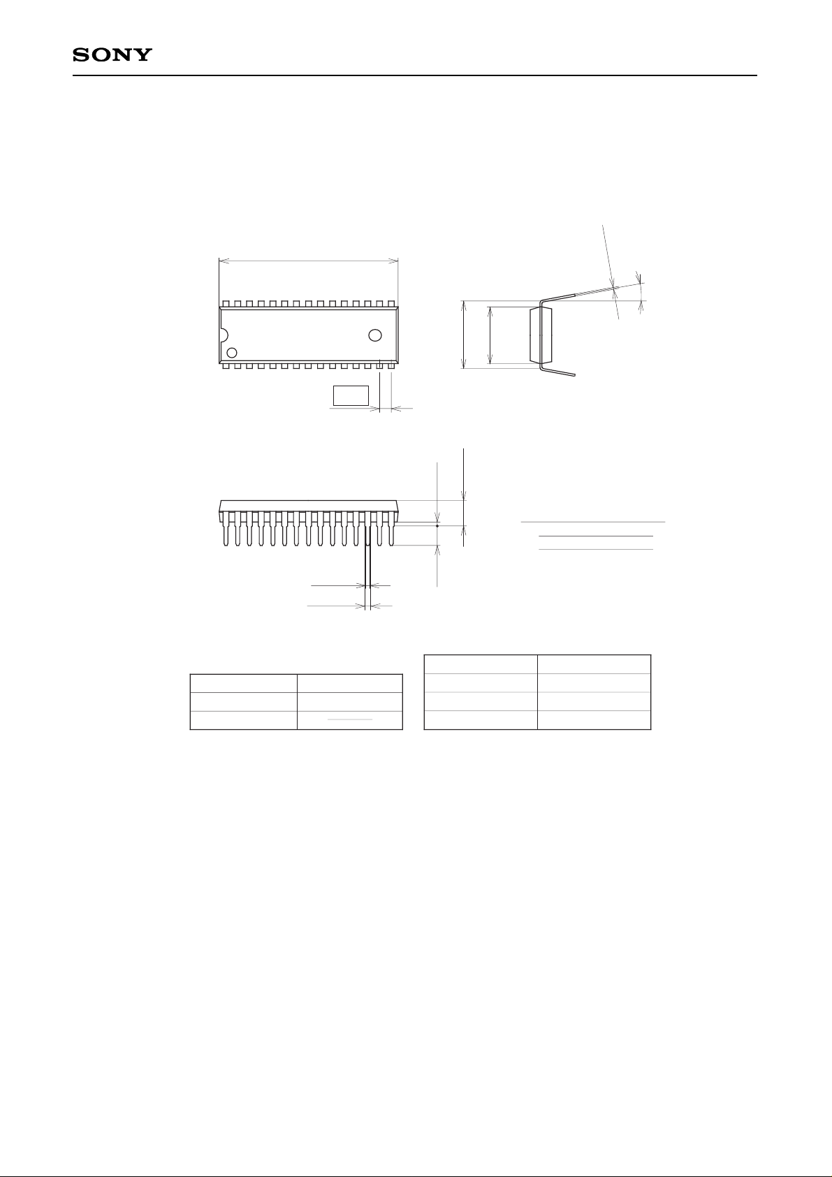
Package Outline Unit: mm
SONY CODE
EIAJ CODE
JEDEC CODE
30PIN SDIP (PLASTIC)
26.9 – 0.1
+ 0.4
15
16
30
1.778
10.16
8.5 – 0.1
+ 0.3
0.25 – 0.05
+ 0.1
0° to 15°
0.5 ± 0.1
0.9 ± 0.15
3.0 MIN
0.5 MIN
3.7 – 0.1
+ 0.4
SDIP-30P-01
SDIP030-P-0400
1
PACKAGE STRUCTURE
MOLDING COMPOUND
LEAD TREATMENT
LEAD MATERIAL
PACKAGE MASS
EPOXY RESIN
PLATING
COPPER ALLOY
1.8g
SOLDER/PALLADIUM
1.All mat surface type.
Two kinds of package surface:
2.All mirror surface type.
 Loading...