

Page 1
CXD2053AM/AS
For the availability of this product, please contact the sales office.
Auto Wide, EDTV-II ID Detection, ID-1 Detection
Description
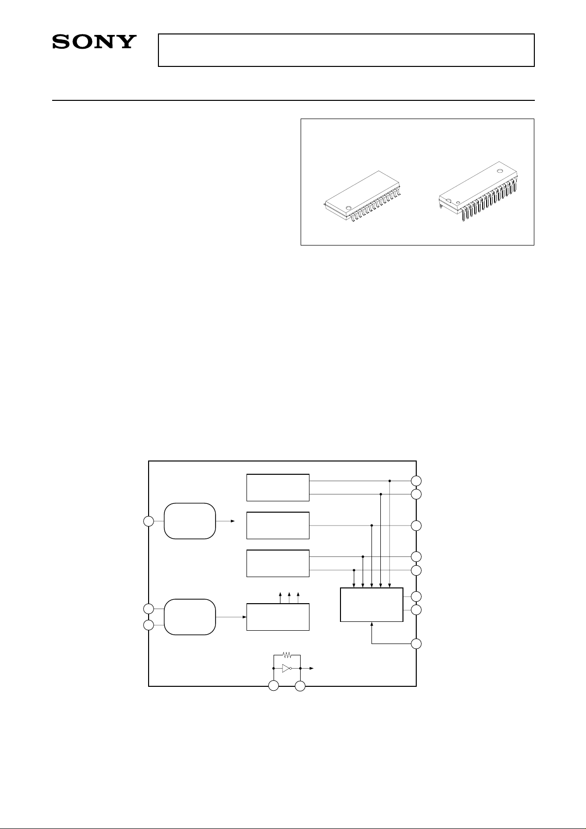
The CXD2053AM/AS is an IC which has the three
functions of identifying the wide video (auto wide),
detecting the EDTV-II ID, and detecting ID-1 (EIAJ,
CPX1024) from the video signal.
Features
• Video aspect ratio identification used with wide
TVs is realized with a single chip.
• I2C bus interface.
This IC can also be used without the bus.
• For auto wide function, 525/60 (NTSC) and 625/50
(PAL, SECAM) can be Supported.
Applications
Wide TV
Structure
Silicon gate CMOS IC
CXD2053AM
28 pin SOP (Plastic)
CXD2053AS
28 pin SDIP (Plastic)
Absolute Maximum Ratings
• Supply voltage VDD VSS – 0.5 to +7.0 V
• Input voltage VI VSS – 0.5 to VDD + 0.5 V
• Output voltage VO VSS – 0.5 to VDD + 0.5 V
• Storage temperature
Tstg –55 to +150 °C
Recommended Operating Conditions
• Supply voltage VDD 4.5 to 5.5 V
• Operating temperature
Topr –20 to +70 °C
Block Diagram
ADIN
VDIN
VSIN
2
11
10
AD Converter
Data Slice Sync
Separator
Auto wide
Identification
EDTV-II
ID Decoder
ID-1 Decoder
Timing Signal
Generator
22
XI
26
OAW1
27
OAW2
OED
28
25
O164
24
OLBX
SCL
I2C Bus Interface
21
XO
15
16
SDA
19
MCON
Sony reserves the right to change products and specifications without prior notice. This information does not convey any license by
any implication or otherwise under any patents or other right. Application circuits shown, if any, are typical examples illustrating the
operation of the devices. Sony cannot assume responsibility for any problems arising out of the use of these circuits.
– 1 –
E96531-ST
Page 2
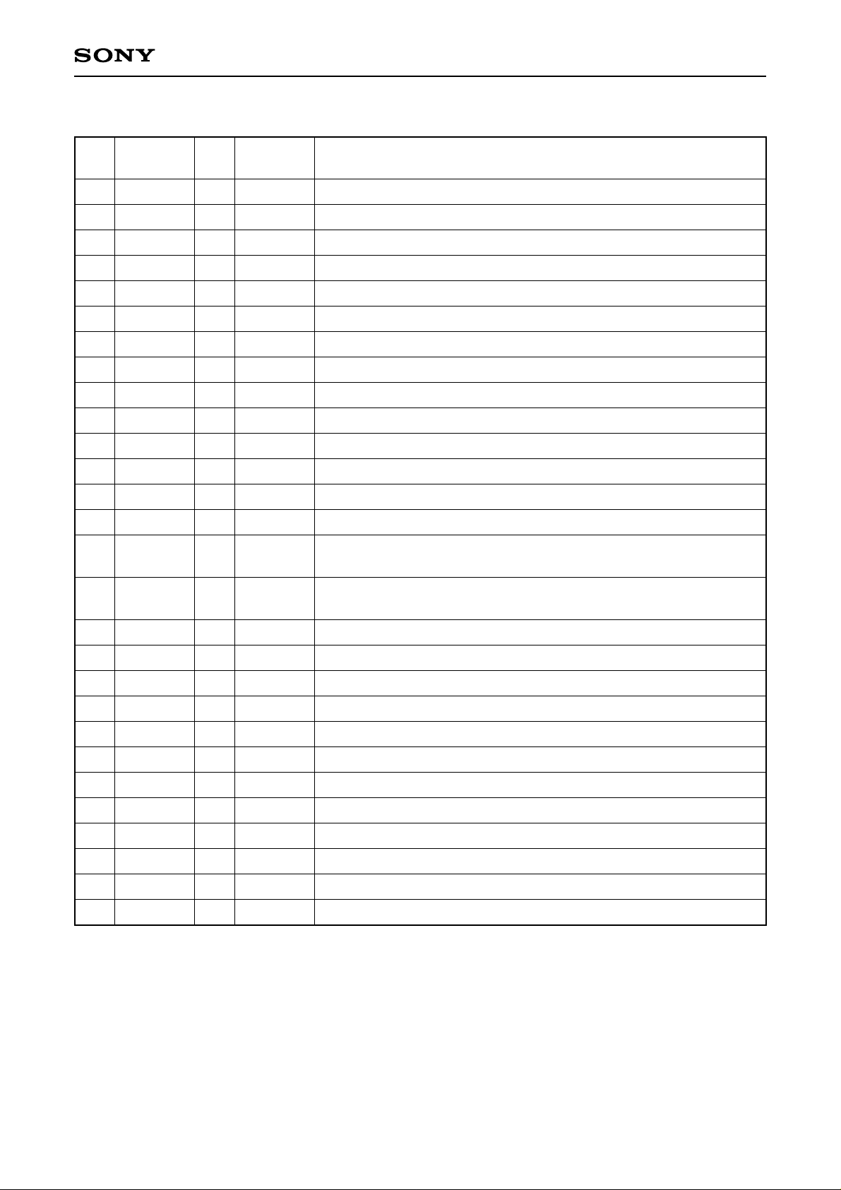
Pin Description
CXD2053AM/AS
Pin
No.
1
2
3
4
5
6
7
8
9
10
11
12
13
14
15
Symbol I/O I/O level Description
AVDD
ADIN
AVSS
CPV
VRB
VRT
CCP
ISET
AVDD
VSIN
VDIN
AVSS
TST1
TST2
SCL
[EDDEC2]
I
I
I
I
I
I
I
I
I
I
I
ANALOG
ANALOG
ANALOG
ANALOG
ANALOG
ANALOG
ANALOG
ANALOG
ANALOG
ANALOG
∗
2
TTL
∗
2
TTL
CMOS
∗1
Analog power supply.
AD converter input.
Analog ground.
Clamp voltage.
AD converter bottom voltage.
AD converter top voltage.
AD converter clamp integrating capacitor connection.
Bias current setting.
Analog power supply
Sync separation input.
Data slicer input.
Analog ground.
Test input; connect to VSS.
Test input; connect to VSS.
I2C bus clock [EDTV-II decoding identification switching]
SDA
16
[ED2FSC]
17
VSS
18
XRST
19
MCON
20
VDD
21
XO
22
XI
23
VSS
24
OLBX
25
O164
26
OAW1
27
OAW2
28
OED
∗1
Schmitt input
∗2
With pull-down resistor
∗3
Open drain
I/O
I
I
O
I
O
O
O
O
O
CMOS
TTL
TTL
CMOS
CMOS
CMOS
CMOS
CMOS
CMOS
CMOS
∗1, 3
I2C bus data [EDTV-II 3.58 M check existence]
Digital ground.
∗
1
Reset at 0.
I2C bus-free mode switching; 0 = I2C-free.
Digital system power supply.
Oscillator connection (14.318MHz).
Oscillator connection or clock input.
Digital ground.
VB-ID detection output; 1 = letter-box, 0 = normal.
VB-ID detection output; 1 = full mode.
Auto wide identification output; 1 = wide video subtitles not present.
Auto wide identification output; 1 = wide video subtitles present.
EDTV-II ID bit 3 detection output.
Note) In I2C-free mode when Pin 19 (MCON) = 0, Pins 15 and 16 switch to the functions in parentheses [ ].
– 2 –
Page 3
CXD2053AM/AS
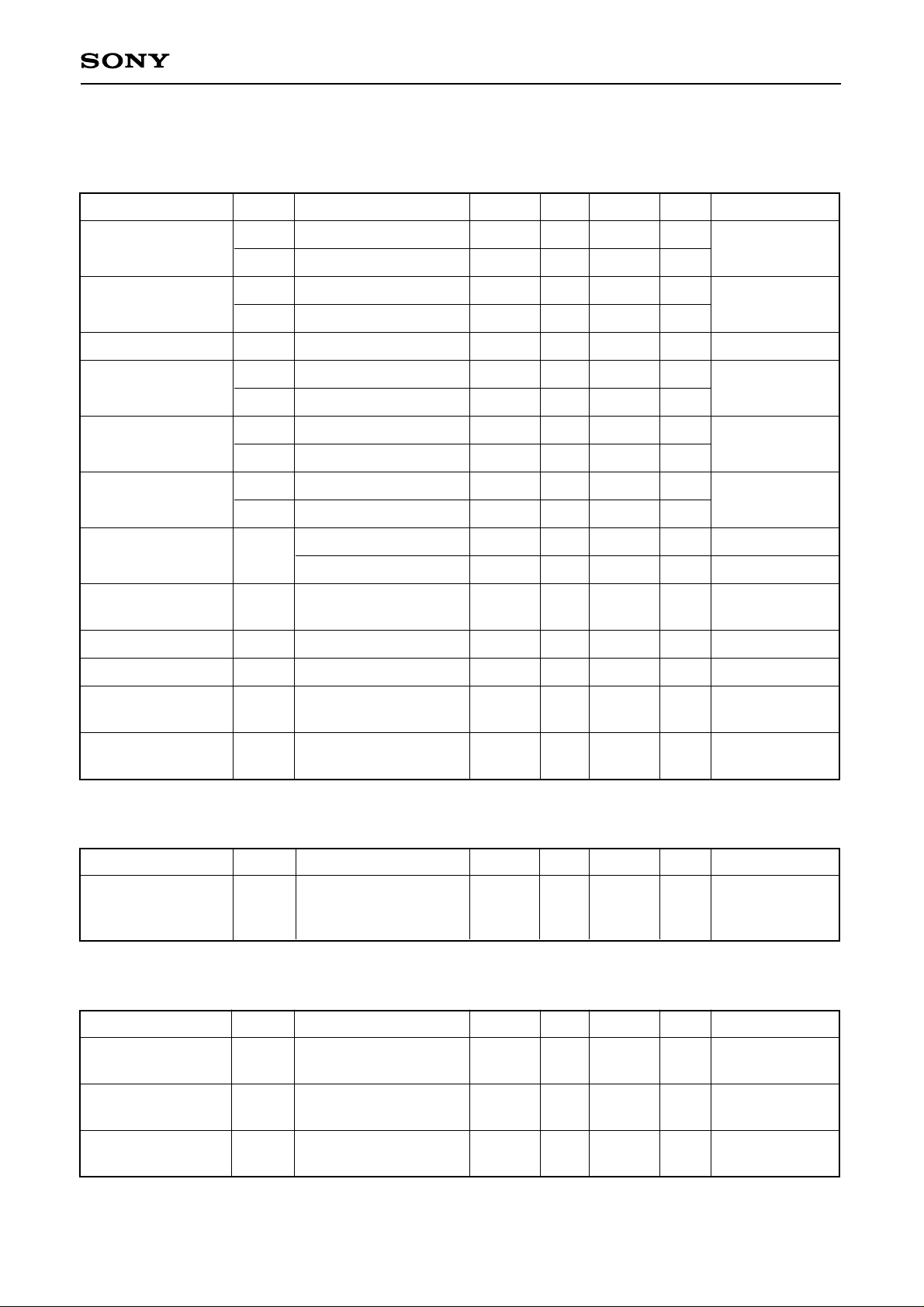
Electrical Characteristics
DC Characteristics (Logic Section) (VDD = 5.0V, VSS = 0V, Ta = 25°C)
Item
Output voltage
Output voltage
Output voltage
Input voltage
Input voltage
Input voltage
Input hysteresis
width
Input leak current
Output leak current
Symbol Condition Min. Typ. Max. Unit Remarks
VOH
VOL
VOH
IOH = –2mA
IOL = 4mA
IOH = –3mA
VDD – 0.8
VDD/2
0.4
V
Pins 24, 25, 26,
27 and 28
V
V
Pin 21 only
VOL
VOL
VIH
VIL
VIH
IOL = 3mA
IOL = 3mA
2.2
0.7 × VDD
VDD/2
0.4
0.8
V
V
Pin 16 only
V
Pins 13, 14, 18
and 19
V
V
Pin 22 only
VIL
VIH
0.8 × VDD
0.3 × VDD
V
V
Pins 15 and 16
VIL
0.05 ×VDD
0.2 × VDD
V
V
Pins 15 and 16
Vhys
Ii
IOZ
VIN = either VSS or VDD
VIN = eother VSS or VDD
–10
–40
0.4
+10
+40
V
Pin 18
Except for Pins
µA
13, 14 and 22
µA
Pin 16 only
Input current
Feedback resistor
Current consumption
Ii
Rfbk
IDD
VIN = VDD
XI (Pin 22) = either
VDD or VSS
Clock 14.318MHz
40
250k
100
1M
29
240
2.5M
µA
Ω
mA
Pins 13 and 14
Between Pins 21
and 22
Sum of Pins 1, 9
and 20
AC Characteristics (VDD = 5.0V, VSS = 0V, Ta = 25°C)
Item
Symbol Condition Min. Typ. Max. Unit Remarks
Pin 22 input, or
Clock frequency fxi
14.318
MHz
oscillator between
Pins 21 and 22
I/O Pin Capacitance
Item
Input pin
capacitance
Output pin
capacitance
Symbol Condition Min. Typ. Max. Unit Remarks
CIN
COUT
VDD = VI = 0V,
f = 1MHz
VDD = VI = 0V,
f = 1MHz
9
11
pF
pF
Input/output pin
capacitance
CI/O
VDD = VI = 0V,
f = 1MHz
– 3 –
11
pF
Page 4
CXD2053AM/AS
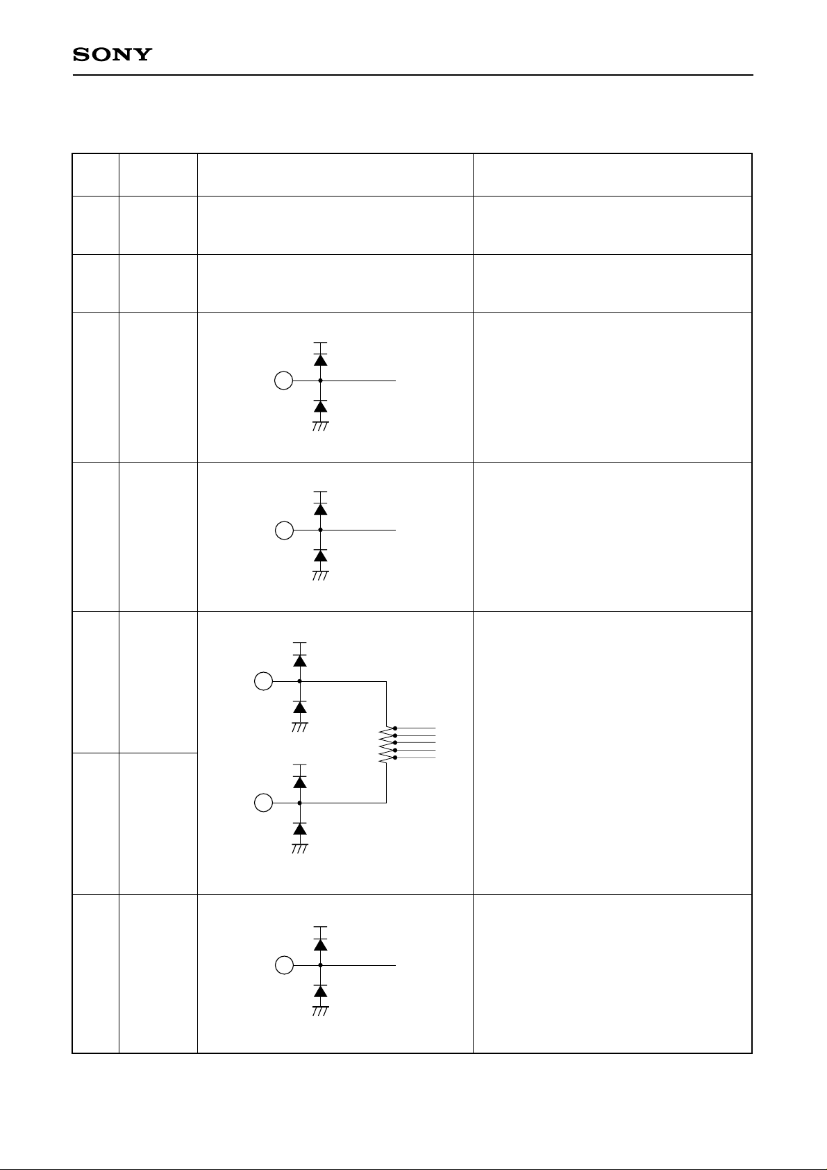
Pins and Electrical Characteristics
Analog Section (VDD = 5.0V, VSS = 0V, Ta = 25°C)
Pin
No.
1
3
2
4
Symbol Equivalent circuit Description
AD converter analog power supply.
Connect a low-noise power supply from the
digital system.
AD converter analog ground.
Connect to the same potential as other VSS
and AVSS.
AVDD
AVSS
Not connected to VDD (Pin 20) or AVDD
(Pin 9) inside the IC.
Not connected to VSS (Pins 17 and 23) or
AVSS (Pin 12) inside the IC.
AVDD
AD converter input.
ADIN
2
This pin is pedestal clamped to the
potential of CPV (Pin 4), so input the video
signal with capacitor coupled.
AVSS
AVDD
CPV
4
ADIN (Pin 2) pedestal clamp voltage
setting.
AVSS
AVDD
5
VRB
6
AVSS
AVDD
AD converter input range setting.
The resistor between Pins 5 and 6 is 310Ω
(Typ.).
5
6
VRT
AVSS
AVDD
7
CCP
7
Clamp circuit integrating capacitor
connection. Connect 0.022µF between this
pin and AVSS (Pin 3).
AVSS
– 4 –
Page 5
CXD2053AM/AS
Pin
No.
9
12
8
10
Symbol Equivalent circuit Description
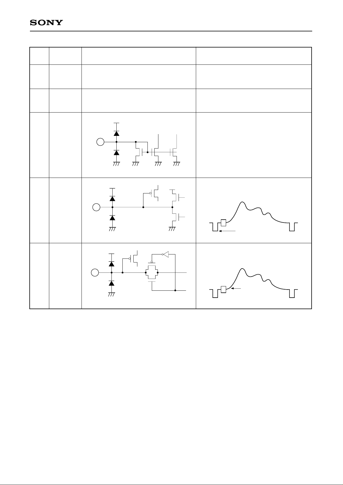
Sync separation system analog power supply.
Connect a low-noise power supply from the
digital system.
Sync separation system analog ground.
Connect to the same potential as other VSS
and AVSS.
Bias setting.
Connect to AVDD (Pin 9) with 33kΩ.
Chip clamp, sync separation input.
AVDD
AVSS
ISET
Not connected to VDD (Pin 20) or AVDD
(Pin 1) inside the IC.
Not connected to AVSS (Pin 3) or VSS
(Pins 17 and 23) inside the IC.
AVDD
8
AVSS
AVDD
Input with capacitor coupled.
VSIN
10
11
VDIN
11
AVSS
AVDD
AVSS
Clamp voltage 1.5V
Pedestal clamp, ID-1 data slicer input.
Input with capacitor coupled.
Clamp voltage
1.5V
– 5 –
Page 6

CXD2053AM/AS
1. Description of auto wide function
The auto wide function performs wide screen identification from the black bands at the top and bottom of the
screen. As shown below, the CXD2053AM/AS identifies the three types of 4:3 normal video, 16:9 wide video,
and wide video with subtitles.
4:3 normal video 16:9 wide video Wide video with subtitles
Fig. 1. Wide identification types
The results of this auto wide identification are expressed by 2 bits, and are output through the I2C bus during
bus mode. Also, these results are output directly to the OAW1 (Pin 26) and OAW2 (Pin 27) pins regardless of
bus or bus-free mode.
Auto wide identification is provided with a transition time of about 1 to 15 seconds to prevent misoperation.
During I2C bus mode, wide identification can be changed quickly without this transition time by manipulating
the INST bit.
2. Description of ID-1 (transmitter method of additional video information, aspect ratio identification)
As shown in the table below, the additional video information consists of 14-bit data, to which a 6-bit CRCC is
appended for a total of 20 bits. On an NTSC video signal, this information is carried on lines 20 and 283 of the
vertical blanking interval.
bit-No
Description
"1" "0"
1
A
2
3
Transmitter aspect ratio
Pictorial representation format
Undefined
Full mode (16:9)
Letter-box
4:3
Normal
WORD0
WORD1
WORD2
B
4
5
6
4-bit width
4-bit width
Discrimination information about the video signal and any other signal (audio
signal, etc.) incident to the video and transmitted simultaneously.
Word 0 dependent discrimination signal
Word 0 dependent discrimination signal, information, etc.
(From the Provisional Standard of EIAJ, CPX-1204)
Table 1. Description of ID-1 signal
Of the 14-bit data noted above, only the first 2 bits are handled by the CXD2053AM/AS. These 2 bits are
obtained by the I2C bus during bus mode. Also, these bits are output directly to the OLBX (Pin 24) and O164
(Pin 25) regardless of bus or bus-free mode.
– 6 –
Page 7

CXD2053AM/AS
3. Description of EDTV-II ID
As shown in the table below, EDTV-II ID consists of 27-bit data. On an NTSC video signal, this information is
carried on lines 22 and 285 of the vertical blanking interval.
Bit
No.
1
Reference signal
2
Reference signal
3
Letter-box
4
Parity of bits 3 and 5
5
Undefined
6
Field No.
7
Multiphase
8
VT
9
VH
10
HH
11
HH precombing
12
Broadcasting station operation bit
13
Broadcasting station operation bit
14
Broadcasting station operation bit
Description
01
—
0
Full line
0
0
1
A
No
No
No
No
1
—
Letter-box
1
—
2
B
Yes
Yes
Yes
Yes
Bit
No.
15
16
17
18
19
20
21
22
23
24
25
26
27
Description
Undefined
Undefined
Undefined
Error correction signal
Error correction signal
Error correction signal
Error correction signal
Error correction signal
Error correction signal
0
Confirmation sine wave
Confirmation sine wave
Confirmation sine wave
01
—
—
—
—
—
—
0
—
Table 2. Description of EDTV-II ID (discrimination control signal) signal
Of the 27 bits noted above, the CXD2053AM/AS outputs only bits 3 and 5. These 2 bits are obtained by the I2C
bus during bus mode. Also, bit 3 only is output directly to the OED (Pin 28) regardless of bus or bus-free mode.
Since the CXD2053AM/AS does not perform decode processing for bits 6 to 23, this results in simple
identification which does not use the error correction signals.
4. Clock
The CXD2053AM/AS requires a 4fsc clock (14.318MHz). Connect XI (Pin 22) and XO (Pin 21) when using a
crystal oscillator.
When inputting the clock from an external source, input to XI (Pin 22).
Clock is 14.318MHz regardless of switching auto wide 525/60 (NTSC) or 625/50 (PAL, SECAM).
5. Settings and data input/output
The CXD2053AM/AS settings and data input/output can be performed by direct setting by pins or with the I2C
bus interface.
– 7 –
Page 8

CXD2053AM/AS
5-1. I2C bus
Settings and data can be taken out via the I2C bus when MCON (Pin 19) is set to "1".
This LSI supports the I2C bus slave RECEIVER and slave TRANSMITTER modes. The slave address is 1C (H).
Also, in addition to standard mode (Max. 100K bit/s), this LSI also supports high-speed mode (Max. 400K bit/s).
Even when the IC power supply falls to 0V, it does not occupy the bus. However, the Absolute Maximum
Ratings should be strictly observed.
The I2C bus transfer sequence is shown in the figure below.
The amount of data transferred by this IC is 2 bytes for the write (RECEIVER) side and 1 byte for the readout
(TRANSMITTER) side.
Data write (RECEIVER mode)
7654321 0 1 76543210 1 176543210
Sm SLAm
Wm As DATAm As DATAm As P
Data readout (TRANSMITTER mode)
7654321 0 1 76543210 1
Sm SLAm
Rm As DATAs XAm P
Symbol
∗
m
∗
s
S
P
SLA
DATA
W
R
A
from master to slave
from slave to master
Start Condition
Stop Condition
Slave Address
Data
0: Write Master→ Slave
1: Read Slave → Master
Clock pulse for Acknowledgement (SDA: L)
Description
XA
Acknowledgement none (SDA: H)
– 8 –
Page 9

CXD2053AM/AS
R/W
WR
bit 7 MSB
bit 6
bit 5
bit 4
bit 3
1st byte2nd byte
bit 2
bit 1
bit 0 LSB
bit 7 MSB
bit 6
bit 5
bit 4
bit 3
bit 2
bit 1
Bit
Name Description
ED2FSC
ED2RES
EDDEC1
EDDEC2
VBLNJ1
VBRES
AWRES
INST
No Use
and TEST
UPAREA
0 when checking the 3.58MHz amplitude during EDTV-II ID
decoding; 1 when not checking the amplitude.
EDTV-II ID decoding function reset. 1 = reset.
EDTV-II ID decoding function detection switching.
Standard values: bit 5 = 0, bit 4 = 1.
EDTV-II ID decoding function detection switching.
Standard values: bit 3 = 0, bit 2 = 1.
Decoding not only of line 20 but also of the 1 line before and after line
20 by the ID-1 decoding function. 0 = yes, 1 = line 20 only.
ID-1 decoding function reset. 1 = reset.
Auto wide function reset. 1 = reset to 4:3.
Auto wide switching is performed without the wait time by changing
INST from 0 to 1.
Not used and LSI test bits. Be sure to set all bits to 0.
Normally. Set the same value as that of PAL bit below.
When PAL = 0, UPAREA = 0, etc.
RD
bit 0 LSB
bit 7 MSB
bit 6
bit 5
bit 4
bit 3
1st byte
bit 2
bit 1
bit 0 LSB
PAL
ED2ID
EDVLD
VBID
VBVLD
AWS
Auto wide function switching.
525/60 when PAL = 0 and 625/50 when PAL = 1.
EDTV-II ID decoding results. 3rd bit of the EDTV-II ID.
EDTV-II ID decoding results. 5th bit of the EDTV-II ID.
EDTV-II ID decoding results judgment. Becomes 1 when a valid
EDTV-II ID exists. The above noted ED2ID is output and held
regardless of this judgment.
ID-1 decoding results. 1st bit: full mode bit.
ID-1 decoding results. 2nd bit: letter-box bit.
VB-ID decoding results judgment. Becomes 1 when a valid VB-ID
exists. The above noted VB-ID is output and held regardless of this
judgment.
Auto wide identification results.
For 4:3 video, bit 1 = 0 and bit 0 = 0.
For 16:9 wide video, bit 1 = 0 and bit 0 = 1.
For subtitle video, bit 1 = 1 and bit 0 = 0.
Table 3. List of I2C bus controls
– 9 –
Page 10
CXD2053AM/AS
5-2. Bus-free mode
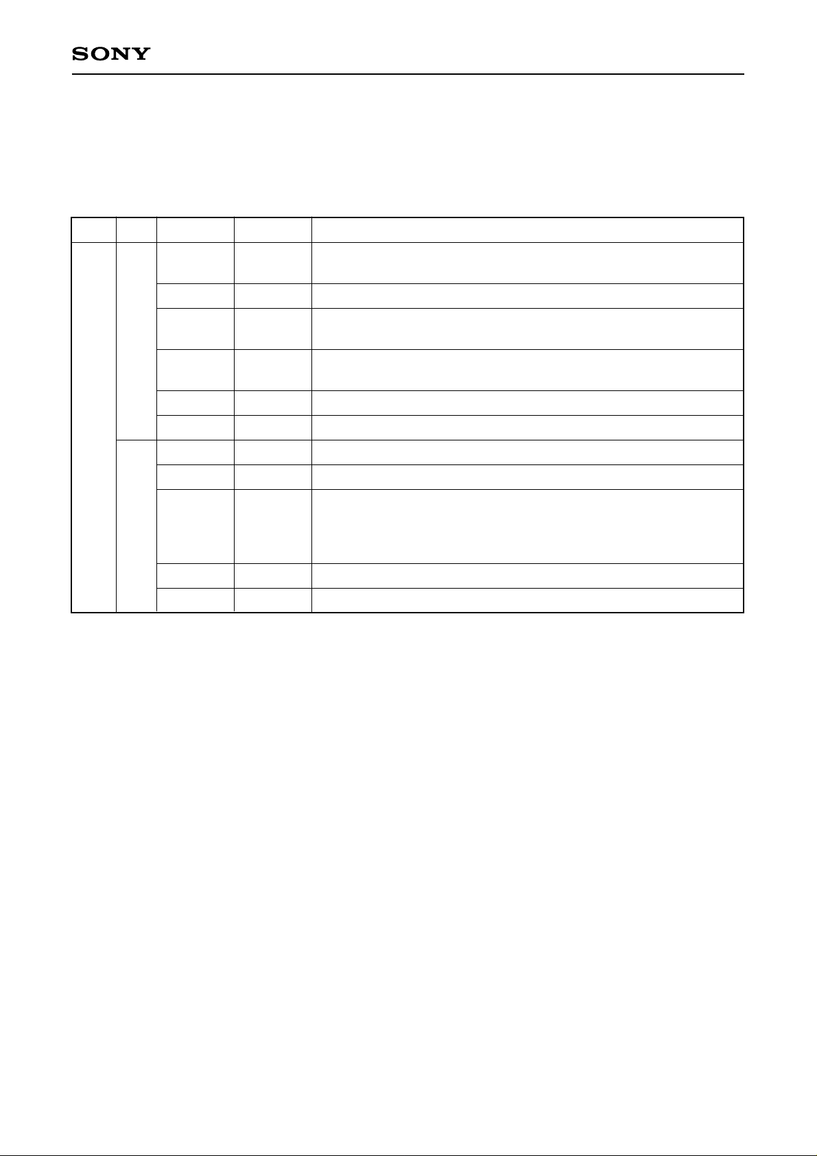
The CXD2053AM/AS can be operated without using the I2C bus when Pin 19 (MCON) is set to 0 and the IC is
switched to bus-free mode.
In this case, the contents normally set by the I2C are fixed to the values below.
Also, only the two functions listed in the table below can be switched by Pins 15 (SCL) and 16 (SDA).
Bit
bit 7 MSB
bit 6
bit 5
bit 4
1st byte2nd byte
bit 3
bit 2
bit 1
bit 0 LSB
bit 7 MSB
C setting information
2
I
bit 6
bit 5
bit 4
bit 3
bit 2
bit 1
bit 0 LSB
Name Description
ED2FSC
ED2RES
EDDEC1
EDDEC2
VBLNJ1
VBRES
AWRES
INST
No Use
and TEST
UPAREA
PAL
Directly controlled by Pin 16 (SDA).
The unmodified SDA pin level becomes ED2FSC.
ED2RES = 0
bit5 = 0, bit4 = 1.
Directly controlled by Pin 15 (SCL).
When SCL = 0, bit 3 = 0 and bit 2 = 1. When SCL = 1, bit 3 = 1 and bit 2 = 0.
VBLNJ1 = 0
VBRES = 0
AWRES = 0
INST = 0
All 0
UPAREA = 0
PAL = 0 Fixed to 525/60 mode.
Table 4. Setting values during bus-free mode (Pin 19 (MCON) = 0)
– 10 –
Page 11

6. Processing of EDTV-II ID and ID-1 data from the bus
EDTV-II ID
or ID-1
Decoder
CXD2053AM/AS
Pin direct output
Data validity judgment
CXD2053AM/AS
EDVLD or
VBVLD
2
I
C
to microcomputer
As shown in the figure above, the data validity judgment and decoding results are obtained independently
during EDTV-II ID or ID-1 decoding. When outputting these results directly to pins, the results are output after
first taking their logical product (AND). These results are output independently to the I2C bus.
Therefore, processing inside the microcomputer which has acquired the information from the I2C is performed
either by simply outputting this data directly to the pins or by taking the logical product (AND) as above.
In addition, performing the processing when the data validity judgment result (EDVLD or VBVLD) is 1 and the
decoding result is 0 allows video to be judged as 4:3 video. Even video which has had the top and bottom of
the screen blacked out due to picture composition intentions can be viewed as the original 4:3 video by giving
this judgment priority over the auto wide function.
7. Setting EDTV-II ID decoding function
The performance of the EDTV-II ID decoding function can be switched directly by pin settings during either I2C
bus or bus-free mode.
I2C exists
ED2FSC = 0
EDDEC2 bit3 = 0, bit2 = 1
ED2FSC = 0
EDDEC2 bit3 = 1, bit2 = 0
ED2FSC = 1
EDDEC2 bit3 = 1, bit2 = 0
Setting
I2C -free
Resistance to ghosting
Resistance to weak
electric fields
SCL (15pin) = Low
SDA (16pin) = Low
Medium
Medium
SCL (15pin) = High
SDA (16pin) = Low
Strong
Medium
SCL (15pin) = High
SDA (15pin) = High
Strong
Strong
Table 5. EDTV-II ID decoding function switching
ED2FSC is originally a function which stops the 3.58MHz amplitude check for the Y signal input from the S
terminal, etc. However, it can also be used in combination with the EDDEC2 setting to increase the resistance
to ghosting and weak electric fields as shown in the table above. EDDEC2 is the luminance check level
switching during the 3.58MHz or 2.04MHz confirmation signal interval.
Similarly, although EDDEC1 is the 2.04MHz amplitude check level switching, it should be set to bit 5 = 0 and
bit 4 = 1.
Since EDTV-II ID identification for this IC is simple identification, increasing the resistance to weak electric
fields, etc. results in a tradeoff which increases the possibility of misoperation. Accordingly, the leftmost
settings in the table above should be used as the standard settings, and other settings used only when
necessary.
– 11 –
Page 12
CXD2053AM/AS
8. Judgment time during auto wide and shortening this time
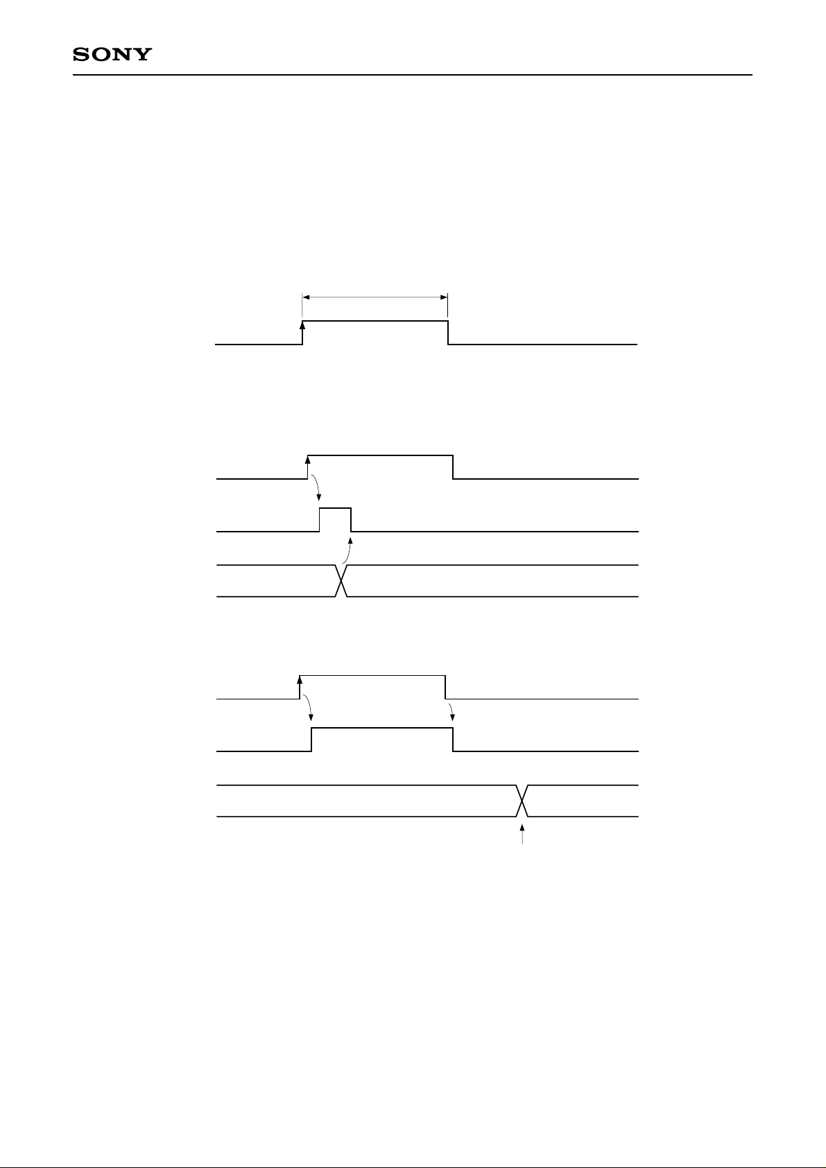
An appropriate judgment transition wait time is provided during auto wide in order to prevent misjudgments.
During I2C bus mode, this transition time can be shortened as necessary using the INST bit.
At the rising edge of INST, the screen changes without waiting to the screen being judged at that time.
The INST pulse width should be set to 3 fields or more as shown below.
3 fields (50ms) or more
INST
The wait time-free status ends with the auto wide judgment transition or when INST becomes 0. This situation
is illustrated in the figure below.
INST
Wait time-free status
(inside the IC)
Auto wide identification
INST
Wait time-free status
(inside the IC)
Auto wide identification No screen change
Transition time wait
After transition
Transition time wait
The screen change here.
INST does not
function.
– 12 –
Page 13

Direct output
(open when not used)
CXD2053AM/AS
C
2
I
22p
Z
22p
14.3MH
20
9
1
33k
DD
DD
DD
AVSS
3
V
AV
19
MCON
AV
AVSS
12
18
XRST
ISET
8
28
OED
VRT
6
24
OLBX
25
O164
CPV
4
27
26
OAW2
OAW1
16
SDA
CXD2053AM/AS
VRB
CCP
5
7
0.022µ
15
SCL
100
13
TST1
ADIN
2
14
TST2
470p
17
SS
V
100
23
VSS
VSIN
10
10
1000p
21
XO
22
XI
VDIN
11
100
60 to 80mA
DD = 5.0V ± 5%
V
Application Circuit
100
2.2k
0.01µ
100
2.0Vp-p
100 IRE
33
0.01µ
0 IRE
15
10µ
–40 IRE
100
1µ
100
0.1µ
Application circuits shown are typical examples illustrating the operation of the devices. Sony cannot assume responsibility for
any problems arising out of the use of these circuits or for any infringement of third party patent and other right due to same.
10µ
3.3k
in
V
10k
– 13 –
Page 14

Package Outline Unit: mm
CXD2053AM
CXD2053AM/AS
28PIN SOP (PLASTIC) 375mil
1
SONY CODE
EIAJ CODE
JEDEC CODE
+ 0.4
18.8 – 0.1
0.45 ± 0.1
SOP-28P-L04
∗SOP028-P-0375-D
1528
14
1.27
M
± 0.12
PACKAGE STRUCTURE
PACKAGE MATERIAL
LEAD TREATMENT
LEAD MATERIAL
PACKAGE WEIGHT
+ 0.3
7.6 – 0.1
10.3 ± 0.4
2.3 – 0.15
9.3
+ 0.1
0.2 – 0.05
EPOXY / PHENOL RESIN
SOLDER PLATING
42 ALLOY
0.7g
+ 0.4
+ 0.2
0.1 – 0.05
0.5 ± 0.2
0.15
CXD2053AS
28PIN SDIP (PLASTIC) 400mil
+ 0.4
26.9 – 0.1
28 15
– 0.1
+ 0.3
10.16
8.5
114
1.778
– 0.1
+ 0.4
0.5 MIN
3.7
SONY CODE
EIAJ CODE
JEDEC CODE
0.5 ± 0.1
0.9 ± 0.15
SDIP-28P-01
SDIP028-P-0400-A
3.0 MIN
PACKAGE STRUCTURE
PACKAGE MATERIAL
LEAD TREATMENT
LEAD MATERIAL
PACKAGE WEIGHT
– 0.05
+ 0.1
0.25
0° to 15°
EPOXY RESIN
SOLDER PLATING
COPPER / 42 ALLOY
1.7g
– 14 –
 Loading...