

Page 1

DBS Audio Signal Processor
For the availability of this product, please contact the sales office.
CXD2027Q/R
Description
The CXD2027Q/R are audio signal processors
designed for DBS applications. These LSIs perform
all digital processing from QPSK demodulation to
analog audio output on a single chip.
Features
QPSK and PCM demodulators and DAC output
are configured on a single chip.
Descrambler interface according to the COATEC
system and SkyPort system .
Functions
QPSK demodulator
• Carrier, clock and data regeneration
• ALC and VCXO adjustment-free
PCM demodulator
• Frame sync protection by correlation detection
• De-interleaving and descrambling
• BCH error correction, range bit error correction
• Audio data range control
Expansion from 10 to 14 bits in A mode
Upper bit majority correction in B mode
• Control sign integration correction, chargeable
flag integration correction by master frame
synchronization
• Interface output for external DAC
• Digital interface output
1-bit DAC output
• Quadruple oversampling filter
• Digital de-emphasis circuit
• 1-bit stereo DAC with 2nd-order ∆∑ format noise
shaper
S/N ratio : 90dB (Typ.)
Distortion: 0.011% (Typ.)
CPU interface
•I2C bus
Descrambler interface
• COATEC system, SkyPort system
Mute functions
• Error occurrence frequency detection mute
• Audio chargeable flag detection mute
• Control sign (B7) detection mute
CXD2027Q
64 pin QFP (Plastic)
Structure
Silicon gate CMOS IC
Applications
TVs, VCRs with built-in BS tuners
Absolute Maximum Ratings (Ta = 25°C, Vss = 0V)
• Supply voltage VDD Vss – 0.5 to +7.0 V
• Input voltage VI Vss – 0.5 to VDD + 0.5V
• Output voltage VO Vss – 0.5 to VDD + 0.5V
• Storage temperature Tstg –55 to +150 °C
Operating Conditions
• Supply voltage VDD 4.75 to 5.25 V
• Operating temperature Topr –20 to +75 °C
CXD2027R
80 pin LQFP (Plastic)
Sony reserves the right to change products and specifications without prior notice. This information does not convey any license by
any implication or otherwise under any patents or other right. Application circuits shown, if any, are typical examples illustrating the
operation of the devices. Sony cannot assume responsibility for any problems arising out of the use of these circuits.
– 1 –
E94808-ST
Page 2

CXD2027Q/R
DATB
DATA
DATO
DSLA
13
MUTE
54
&
SHIFTER
BCH (7, 3)
RANGE BIT
GENERATOR
MUTE SIGNAL
8
9
(63, 56)
BCH DECODER
7
ERROR
MAJORITY
CORRECTION
10 → 14 BIT
DATA EXPAND
LPO
28
CLOCK GENERATOR
32
25
DAC1
DAC2
DE-ENPHASIS
DIGITAL FILTER
35
43
44
AUDIO
INTERFACE
DIGITAL
INTERFACE
LRCK
AUD
RNO
RPO
LNO
BCLK
45
F256
46
15
38
Note) Pin numbers are for the CXD2027R.
TX
SASL
NSYN
BITI
DSLB
BITO
48
DE-SCRAMBLER
AUDIO DATA
INTERPOLATOR
C BUS I/F
2
I
4 kBIT-RAM
DE-INTERLEAVER
FRAME SYNC
5
6
4
DATA
RECOVERY
ADC
SYNC
MASTER FRAME
ALC SIGNAL
GENERATOR
INTEGRAL
CORRECTION
8TH RANGE BIT
INTEGRAL
CORRECTION
CONTROL WORD
CARRIER
RECOVERY
GENERATOR
SYSTEM CLOCK
TIMING
GENERATOR
CLOCK
RECOVERY
51
50
47
14
11
12
56
SCLK
SDA
DTUP
CC1
CK2M
FRAM
MCKO
Block Diagram
71
RT
73
ADIN
76
RB
77
GR
67
ALCO
– 2 –
66
PHAA
65
M23I
64
M23O
58
PHAB
57
MCKI
Page 3

Pin Configuration 1
CXD2027Q
CXD2027Q/R
DD5
V
M23O
M23I
PHAA
ALCO
SS9
V
TST7
RT
ADIN
ADVD
ADVS
RB
GR
SCLK
SDA
3
DD
V
DTUP
NSYN
F256
BCLK
4
DD
V
PHAB
MCKI
8
SS
V
MCKO
TST8
MUTE
7
SS
V
51 50 49 48 47 46 45 44 43 42 41 40 39 38 37 36 35 34 33
52
53
54
55
56
57
58
59
60
61
62
63
64
1 2 3 4 5 6 7 8 9 10111213141516171819
TST0
0
SS
V
MRST
BITO
BITI
DSLB
DSLA
DATB
DATA
0
DD
V
CK2M
FRAM
CC1
DATO
TX
LRCK
TST2
AUD
TST3
TST6
TST4
SASL
TST5
32
31
30
29
28
27
26
25
24
23
22
21
20
SS6
V
SS5
V
RNO
DD2
V
RPO
SS4
V
TST1
SS3
V
LPO
V
DD1
LNO
SS2
V
SS1
V
– 3 –
Page 4

Pin Configuration 2
CXD2027R
CXD2027Q/R
N.C.
N.C.
DD5
V
M23O
M23I
PHAA
ALCO
SS9
V
N.C.
TST7
RT
N.C.
ADIN
ADVD
ADVS
RB
GR
TST0
N.C.
N.C.
N.C.
4
DD
V
PHAB
MCKI
8
SS
V
MCKO
TST8
MUTE
7
SS
V
SCLK
SDA
3
DD
V
DTUP
NSYN
F256
60 59 58 57 56 55 54 53 52 51 50 49 48 47 46 45 44 43 42
61
62
63
64
65
66
67
68
69
70
71
72
73
74
75
76
77
78
79
80
BCLK
LRCK
AUD
TST6
41
N.C.
40
39
38
37
36
35
34
33
32
31
30
29
28
27
26
25
24
23
22
21
N.C.
N.C.
SASL
SS6
V
V
SS5
RNO
N.C.
DD2
V
RPO
SS4
V
TST1
VSS3
LPO
DD1
V
N.C.
LNO
V
SS2
SS1
V
N.C.
N.C.
1 2 3 4 5 6 7 8 9 10111213141516171819
N.C.
0
SS
V
MRST
BITO
BITI
DSLB
DSLA
DATB
DATA
0
DD
V
CK2M
DATO
FRAM
CC1
TX
TST2
TST3
TST4
20
TST5
N.C.
– 4 –
Page 5

Pin Description 1
CXD2027Q (64pin QFP)
CXD2027Q/R
Pin
No.
1
2
3
4
5
6
7
8
9
10
11
12
13
14
15
Symbol I/O Pin Description Remarks
TST0
MRST
VSS Digital
BITO
BITI
DSLB
DSLA
DATB
DATA
VDD Digital
CK2M
FRAM
DATO
CC1
TX
I
Test pin; normally low
I
Master reset; H: normal operation; L: reset
—
Digital ground
O
Bit stream output after PSK demodulation
I
Bit stream input after PSK demodulation
I
External descrambler pin
I
External descrambler pin
I
Data input 2 after BCH correction (for COATEC)
I
Data input 1 after BCH correction (for SkyPort)
—
Digital +5V power supply
O
2.048MHz clock output
O
Frame start bit flag
O
Data output after BCH correction
O
Control sign first bit output
O
Digital format audio output
Internal pull down
Internal pull up
TTL input
TTL input
TTL input
TTL input
TTL input
16
17
18
19
20
21
22
23
24
25
26
27
28
29
30
31
32
TST2
TST3
TST4
TST5
VSS Digital
VSS D/A
LNO
VDD D/A
LPO
VSS D/A
TST1
VSS D/A
RPO
VDD D/A
RNO
VSS D/A
VSS Digital
I
Test pin; normally low
I
Test pin; normally low
I
Test pin; normally low
I
Test pin; normally high
—
Digital ground
—
Analog ground
O
Lch D/A converter output
—
Analog +5V power supply
O
Lch D/A converter output
—
Analog ground
I
Test pin; normally low
—
Analog ground
O
Rch D/A converter output
—
Analog +5V power supply
O
Rch D/A converter output
—
Analog ground
—
Digital ground
Internal pull down
Internal pull down
Internal pull down
Internal pull down
33
34
SASL
TST6
I
I2C bus slave address select (L: D4, H: D6)
I
Test pin; normally low
– 5 –
Internal pull down
Internal pull down
Page 6

CXD2027Q/R
Pin
No.
35
36
37
38
39
40
41
42
43
44
45
46
47
48
49
Symbol I/O Pin Description Remarks
AUD
LRCK
BCLK
F256
DTUP
NSYN
VDD Digital
SDA
SCLK
VSS Digital
TST8
MUTE
VSS Digital
MCKO
MCKI
O
Audio data output for external DF/DAC
O
LR clock output for external DF/DAC
O
Bit clock output for external DF/DAC
O
Clock output for external DF/DAC
O
CCUP: control sign update flag / DED: BCH 2 error detection
O
Asynchronous flag (H: asynchronous; L: synchronous)
—
Digital +5V power supply
I
SDA (I2C bus)
I
SCL (I2C bus)
—
Digital ground
I
Test pin; normally low
I
External forced muting input
—
Digital ground
O
MCKI inversion output
I
24.576MHz clock input
Switched by I2C bus
I2C bus compatible
I2C bus compatible
TTL input
50
51
52
53
54
55
56
57
58
59
60
61
62
63
64
PHAB
VDD Digital
VDD Digital
M23O
M23I
PHAA
ALCO
VSS Digital
TST7
RT
ADIN
VDD A/D
VSS A/D
RB
GR
O
Clock regeneration phase error data output
—
Digital +5V power supply
—
Digital +5V power supply
O
M23I inversion output
I
22.909088MHz clock input
O
Carrier regeneration phase error data output
O
ALC A/D control output
—
Digital ground
I
Test pin; normally low
I
A/D converter VRT input
I
Analog data input
—
Analog +5V power supply
—
Analog ground
I
A/D converter VRB input; connect to analog ground
I
A/D converter VGR input; connect to analog ground
– 6 –
Page 7

Pin Description 2
CXD2027R (80pin LQFP)
CXD2027Q/R
Pin
No.
1
2
3
4
5
6
7
8
9
10
11
12
13
14
15
Symbol I/O Pin Description Remarks
N.C.
MRST
VSS Digital
BITO
BITI
DSLB
DSLA
DATB
DATA
VDD Digital
CK2M
FRAM
DATO
CC1
TX
—
Non-connection
I
Master reset; H: normal operation; L: reset
—
Digital ground
O
Bit stream output after PSK demodulation
I
Bit stream input after PSK demodulation
I
External descrambler pin
I
External descrambler pin
I
Data input 2 after BCH correction (for COATEC)
I
Data input 1 after BCH correction (for SkyPort)
—
Digital +5V power supply
O
2.048MHz clock output
O
Frame start bit flag
O
Data output after BCH correction
O
Control sign first bit output
O
Digital format audio output
Internal pull up
TTL input
TTL input
TTL input
TTL input
TTL input
16
17
18
19
20
21
22
23
24
25
26
27
28
29
30
31
32
TST2
TST3
TST4
TST5
N.C.
N.C.
N.C.
VSS Digital
VSS D/A
LNO
N.C.
VDD D/A
LPO
VSS D/A
TST1
VSS D/A
RPO
I
Test pin; normally low
I
Test pin; normally low
I
Test pin; normally low
I
Test pin; normally high
—
Non-connection
—
Non-connection
—
Non-connection
—
Digital ground
—
Analog ground
O
Lch DAC output
—
Non-connection
—
Analog +5V power supply
O
Lch DAC output
—
Analog ground
I
Test pin; normally low
—
Analog ground
O
Rch DAC output
Internal pull down
Internal pull down
Internal pull down
Internal pull down
33
34
VDD D/A
N.C.
—
Analog +5V power supply
—
Non-connection
– 7 –
Page 8

CXD2027Q/R
Pin
No.
35
36
37
38
39
40
41
42
43
44
45
46
47
48
49
Symbol I/O Pin Description Remarks
RNO
VSS D/A
VSS Digital
SASL
N.C.
N.C.
N.C.
TST6
AUD
LRCK
BCLK
F256
DTUP
NSYN
VDD Digital
O
Rch D/A converter output
—
Analog ground
—
Digital ground
I
I2C bus slave address select (L: D4, H: D6)
—
Non-connection
—
Non-connection
—
Non-connection
I
Test pin; normally low
O
Audio data output for external DF/DAC
O
LR clock output for external DF/DAC
O
Bit clock output for external DF/DAC
O
Clock output for external DF/DAC
O
CCUP: control sign update flag/DED: BCH 2 error detection
O
Asynchronous flag (H: asynchronous; L: synchronous)
—
Digital +5V power supply
Internal pull down
Internal pull down
Switched by I2C bus
50
51
52
53
54
55
56
57
58
59
60
61
62
63
64
65
66
SDA
SCLK
VSS Digital
TST8
MUTE
VSS Digital
MCKO
MCKI
PHAB
VDD Digital
N.C.
N.C.
N.C.
VDD Digital
M23O
M23I
PHAA
I
SDA (I2C bus)
I
SCL (I2C bus)
—
Digital ground
I
Test pin; normally low
I
External forced muting input
—
Digital ground
O
MCKI inversion output
I
24.576MHz clock input
O
Clock regeneration phase error data output
—
Digital +5V power supply
—
Non-connection
—
Non-connection
—
Non-connection
—
Digital +5V power supply
O
M23I inversion output
I
22.909088MHz clock input
O
Carrier regeneration phase error data output
I2C bus compatible
I2C bus compatible
TTL input
67
68
69
70
ALCO
VSS Digital
N.C.
TST7
O
ALC A/D control output
—
Digital ground
—
Non-connection
I
Test pin; normally low
– 8 –
Page 9

CXD2027Q/R
Pin
No.
71
72
73
74
75
76
77
78
79
80
Symbol I/O Description Remarks
RT
N.C.
ADIN
VDD A/D
VSS A/D
RB
GR
TST0
N.C.
N.C.
I
A/D converter VRT input
—
Non-connection
I
Analog data input
—
Analog +5V power supply
—
Analog ground
I
A/D converter VRB input; connect to analog ground
I
A/D converter VGR input; connect to analog ground
I
A/D test pin; normally low
—
Non-connection
—
Non-connection
Absolute Maximum Ratings (Ta = 25°C, Vss = 0V)
Item
Supply voltage
Symbol Ratings Unit
VDD
Vss – 0.5 to +7.0
V
Internal pull down
Input voltage
Output voltage
Operating temperature
Storage temperature
VI
VO
Topr
Tstg
Vss – 0.5 to VDD + 0.5
Vss – 0.5 to VDD + 0.5
–20 to +75
–55 to +150
V
V
°C
°C
I/O Pin Capacitance (VDD = VI = 0V, f = 1MHz)
Item
Input pin capacitance
Output pin capacitance
Input/output pin capacitance
∗1
Input pins other than ∗2and
∗2
SCLK
∗3
BITI, DSLB, DSLA, DATB, DATA, TST5
∗4
All output pins
∗5
SDA
Symbol Min. Typ. Max. Unit Corresponding pins
pF
∗1
∗2
∗3
∗4
∗5
CIN
COUT
CI/O
9
10
11
11
10
∗3
– 9 –
Page 10

CXD2027Q/R
Electrical Characteristics
[DC characteristics] (VDD = 5V ± 0.25V, Vss = 0V, Ta = –20 to +75°C)
Item
Power consumption
Input/output voltage
CMOS input
Input
TTL input
voltage
High level
Low level
Hysteresis voltage
Input rise/fall time
Output voltage
Symbol
PD
VI, VO
VIH
VIL
VIH
VIL
Vt+
Vt–
Vt+ – Vt
tr, tf
VOH
VOL
VOH
VOL
VOH
VOL
Measurement
conditions
VDD = 4.75 to 5.25V
–
IOH = –2mA
IOL = 4mA
IOH = –4mA
IOL = 4mA
IOH = –4mA
IOL = 8mA
Min. Typ. Max. Unit
180
Vss
280
350
VDD
0.7VDD
0.3VDD
2.2
0.8
0.7VDD
0.3VDD
0.5
0
500
VDD – 0.8
0.4
VDD – 0.8
0.4
VDD – 0.8
0.4
mW
V
V
ns
V
Corre-
sponding
pins
∗1
∗2
∗3
∗4
∗5
∗6
∗7
∗8
VOL
VOL
∗1
All pins
∗2
Input pins other than ∗3and
∗3
BITI, DSLB, DSLA, DATB, DATA, MUTE
∗4
SDA, SCLK
∗5
All input pins
∗6
Output pins other than ∗7, ∗8and
∗7
LNO, LPO, RPO, RNO
∗8
BITO, CK2M, FRAM, DATO, CCI, TX
∗9
SDA, SCLK
∗4
∗9
IOL = 3mA
IOL = 6mA
0
0
0.4
0.6
∗9
– 10 –
Page 11
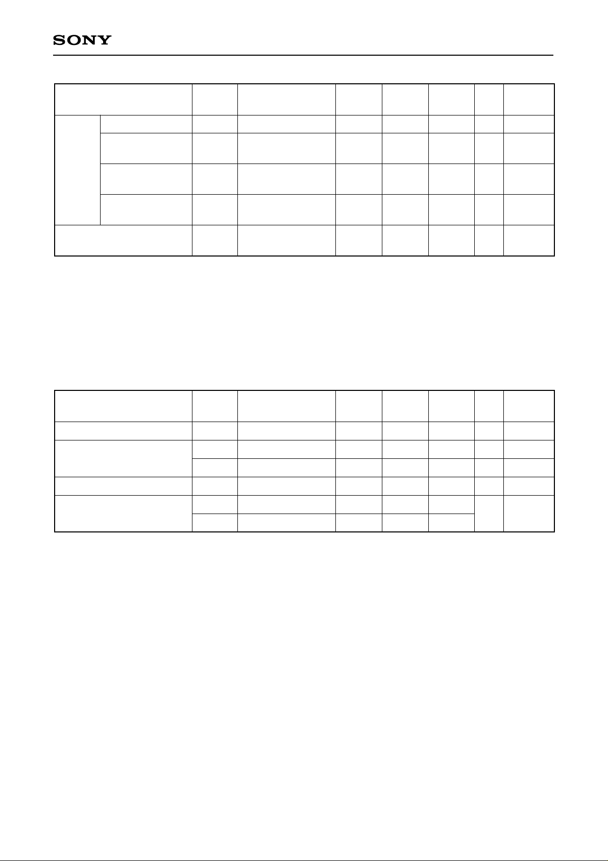
CXD2027Q/R
Item Symbol
Normal input pin
With pull-up
Input
leak
current
resistor
With pull-down
resistor
Bidirectional pin
(during input state)
Output leak current
(I2C bus)
∗1
Input pins other than ∗2, ∗3and
∗2
MRST
∗3
TST0, TST1, TST2, TST3, TST4, SASL, TST6
∗4
BITI, DSLB, DSLA, DATB, DATA, TST5
∗5
SDA, SCLK
II
IIL
IIH
II
IOZ
∗4
Measurement
conditions
VIN = VSS or VDD
VIN = VSS
VIN = VDD
VIN = VSS or VDD
VIN = VSS
Min. Typ. Max. Unit
–10
–40
40
–40
–10
–100
100
10
–240
240
40
–10
µA
µA
µA
µA
µA
Corre-
sponding
pins
∗1
∗2
∗3
∗4
∗5
[Oscillation cell electrical characteristics] (VDD = 5V ± 0.25V, Ta = –20 to +75°C)
Item Symbol
Logic threshold value
Input voltage
Feedback resistance
Output voltage
∗6
MCKI, M23I
∗7
MCKI, MCKO, M23I, M23O
∗8
MCKO, M23O
LVth
VIH
VIL
RFB
VOH
VOL
Measurement
conditions
VIN = VSS or VDD
IOH = –12mA
IOL = 12mA
Min. Typ. Max. Unit
VDD/2
0.7VDD
0.3VDD
250k
1M
2.5M
VDD/2
VDD/2
V
V
V
Ω
V
Corre-
sponding
pins
∗6
∗7
∗8
– 11 –
Page 12
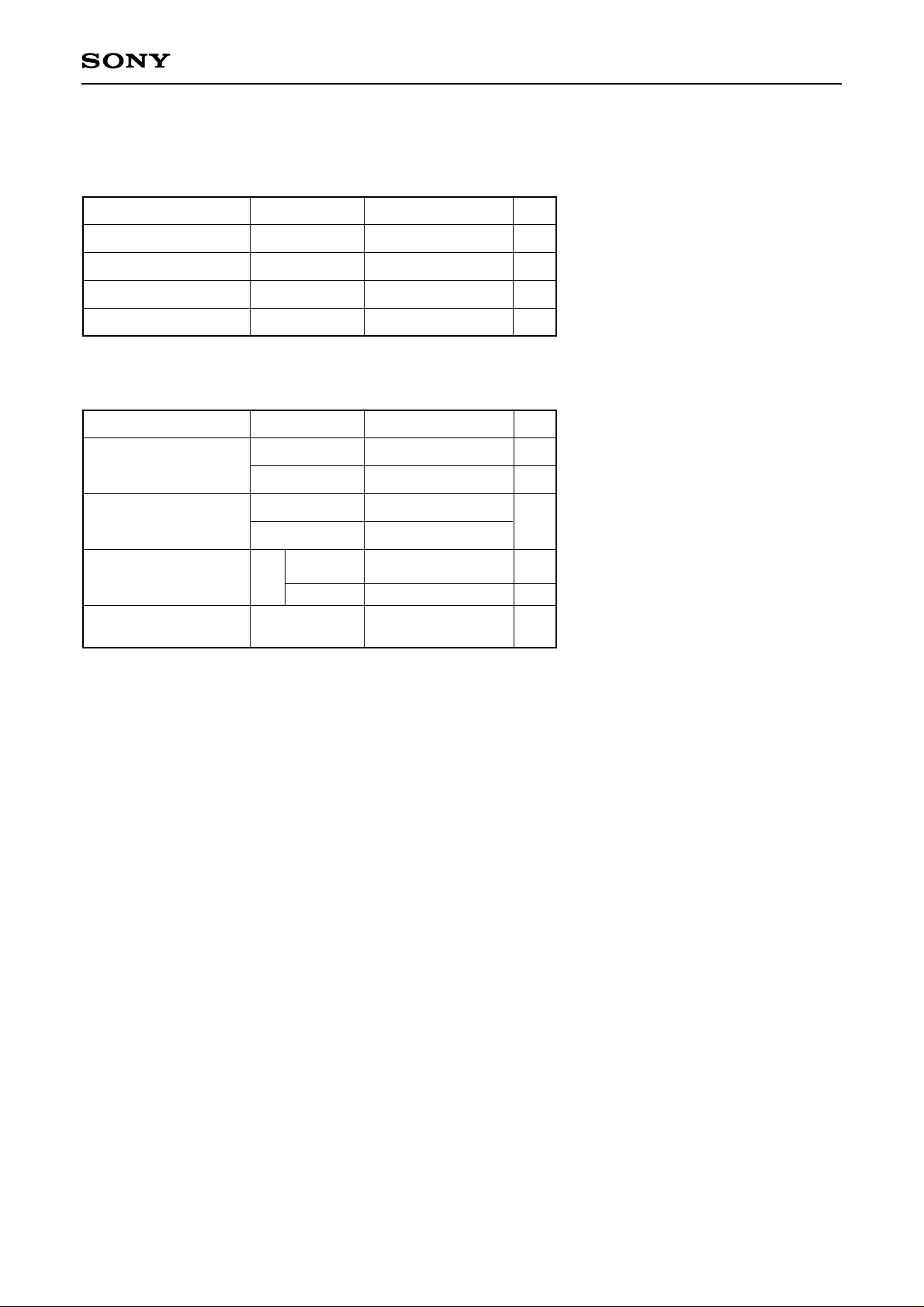
[Internal A/D converter characteristics]
Absolute Maximum Ratings (Ta = 25°C)
CXD2027Q/R
Item
Supply voltage
Input voltage (analog)
Input voltage (digital)
Reference voltage
Operating Conditions
Item
Supply voltage
Reference input
voltage
Analog input
Operating ambient
temperature
Symbol Ratings Unit
AVD
AIN
+7.0
AVD to AVS
VDD to VSS
RB, RT
AVD to AVS
Symbol Ratings Unit
AVD, AVS
l DVS – AVS l
RB
RT
Amplitude
AIN
DC level
Topr
4.75 to 5.25
0 to 100
0 to
to 3.75
100 to 300
(typ. 200)
typ.1.25
–20 to +75
V
V
V
V
V
mV
V
mVp-p
V
°C
– 12 –
Page 13
CXD2027Q/R
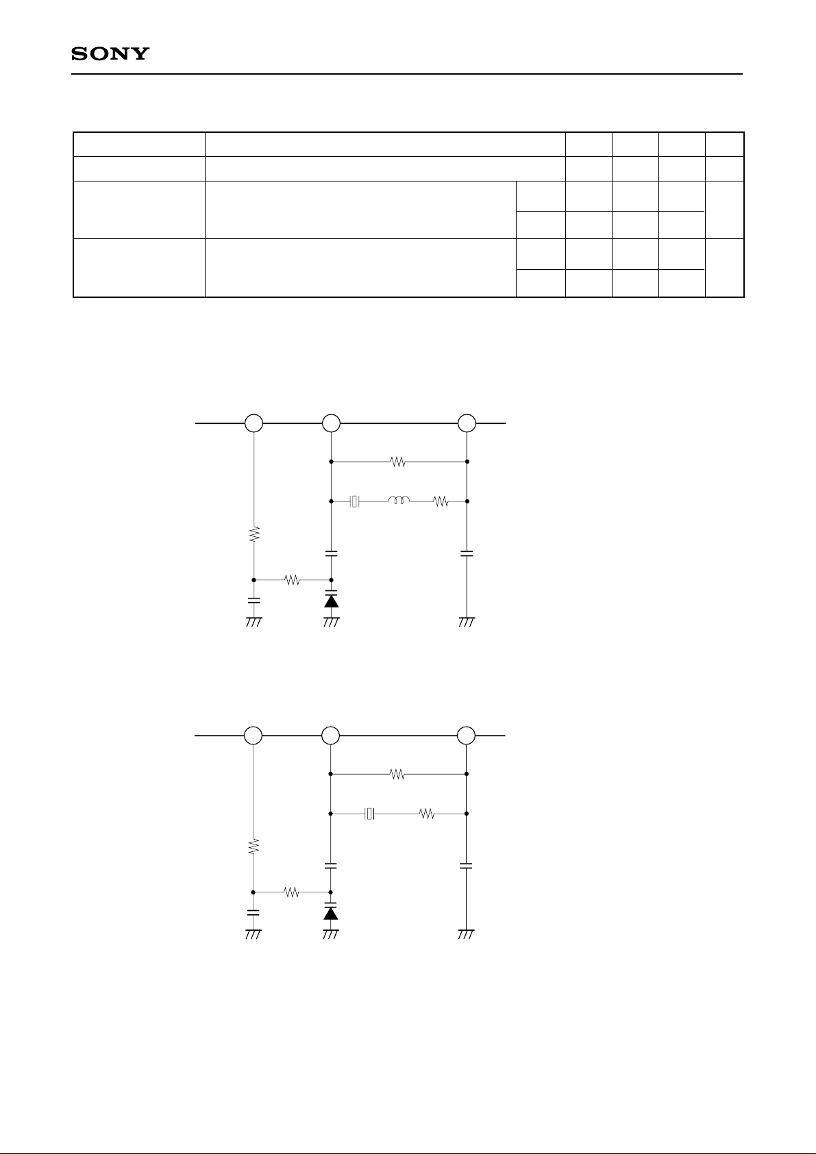
[AC characteristics] (VDD = 5.0V ± 0.25V, Ta = 25°C)
Item
ALC characteristics
Carrier
regeneration
PLL pull-in range
Clock
regeneration
PLL pull-in range
∗
Performance guaranteed only when using constants of the recommended oscillation circuit.
Deviation from standard input level 200mVp-p
Pull-in frequency∗relative to 5.7272MHz.
Includes temperature characteristics (–20 to +75°C)
and supply voltage fluctuation (±5%) of VCXO.
Pull-in frequency∗relative to 2.048MHz.
Includes temperature characteristics (–20 to +75°C)
and supply voltage fluctuation (±5%) of VCXO.
Conditions Min. Typ. Max. Unit
Upper
Lower
Upper
Lower
+750
–450
+300
–100
22.909088MHz (for carrier regeneration PLL) VCXO circuit
PHAA M23I M23O
100K
2.7µ 68
4.7K
22K
390p (CH)
12p (UJ)
±50 %
Hz
Hz
0.01µ
HVU359
24.576MHz (for clock regeneration PLL) VCXO circuit
PHAB MCKI MCKO
100K
4.7K
22K
0.047µ
1800p (CH)
HVU359
330
X'tal
: Daishinku AG8865C
VC
: Hitachi HVU359
L
: Matsushita ELJ-FC series
10p (UJ)
X'talVC: Daishinku AG8865C
: Hitachi HVU359
– 13 –
Page 14
CXD2027Q/R
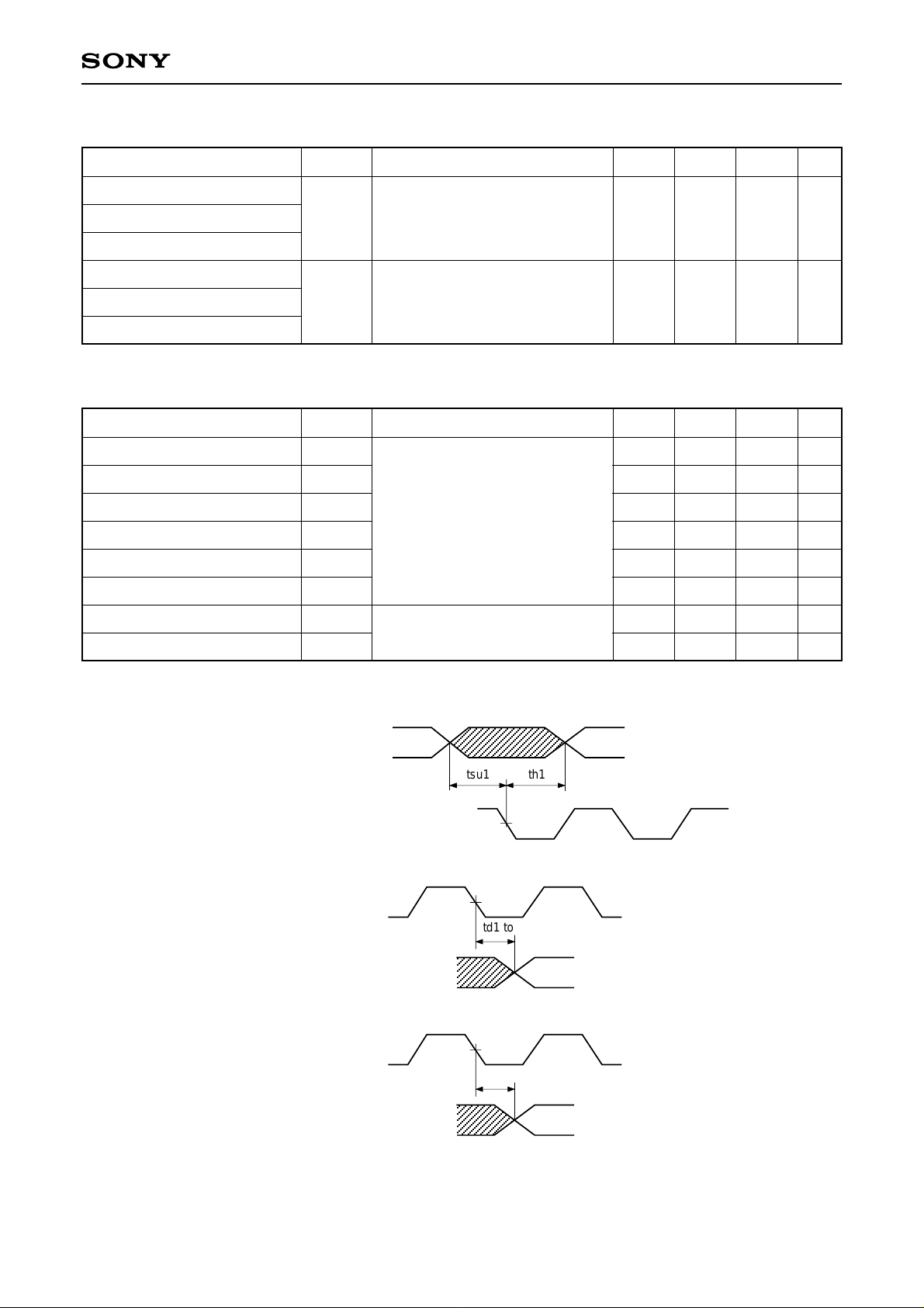
(VDD = 5.0V ± 0.25V, Ta = –20 to +75°C, CL = 60pF)
Item
BITI set-up time
DATA set-up time
DATB set-up time
BITI hold time
DATA hold time
DATB hold time
Item
BITO delay time
DATO delay time
NSYN delay time
FRAM delay time
DTUP delay time
CC1 delay time
Symbol Conditions Min. Typ. Max. Unit
tsu1
th1
Value relative to CK2M fall
Value relative to CK2M fall
32
ns
0
ns
(VDD = 5.0V ± 0.25V, Ta = –20 to +75°C, CL = 60pF)
Symbol Conditions Min. Typ. Max. Unit
td1
td2
td3
td4
td5
td6
17
24
37
Value relative to CK2M fall
23
38
21
ns
ns
ns
ns
ns
ns
AUD delay time
LRCK delay time
td7
td8
BITI, DATA, DATB
CK2M
CK2M
BITO, DATO, NSYN,
FRAM, DTUP, CC1
BCLK
Value relative to BCLK fall
tsu1 th1
td1 to td6
td7 to td8
28
26
ns
ns
AUD, LRCK
– 14 –
Page 15
CXD2027Q/R
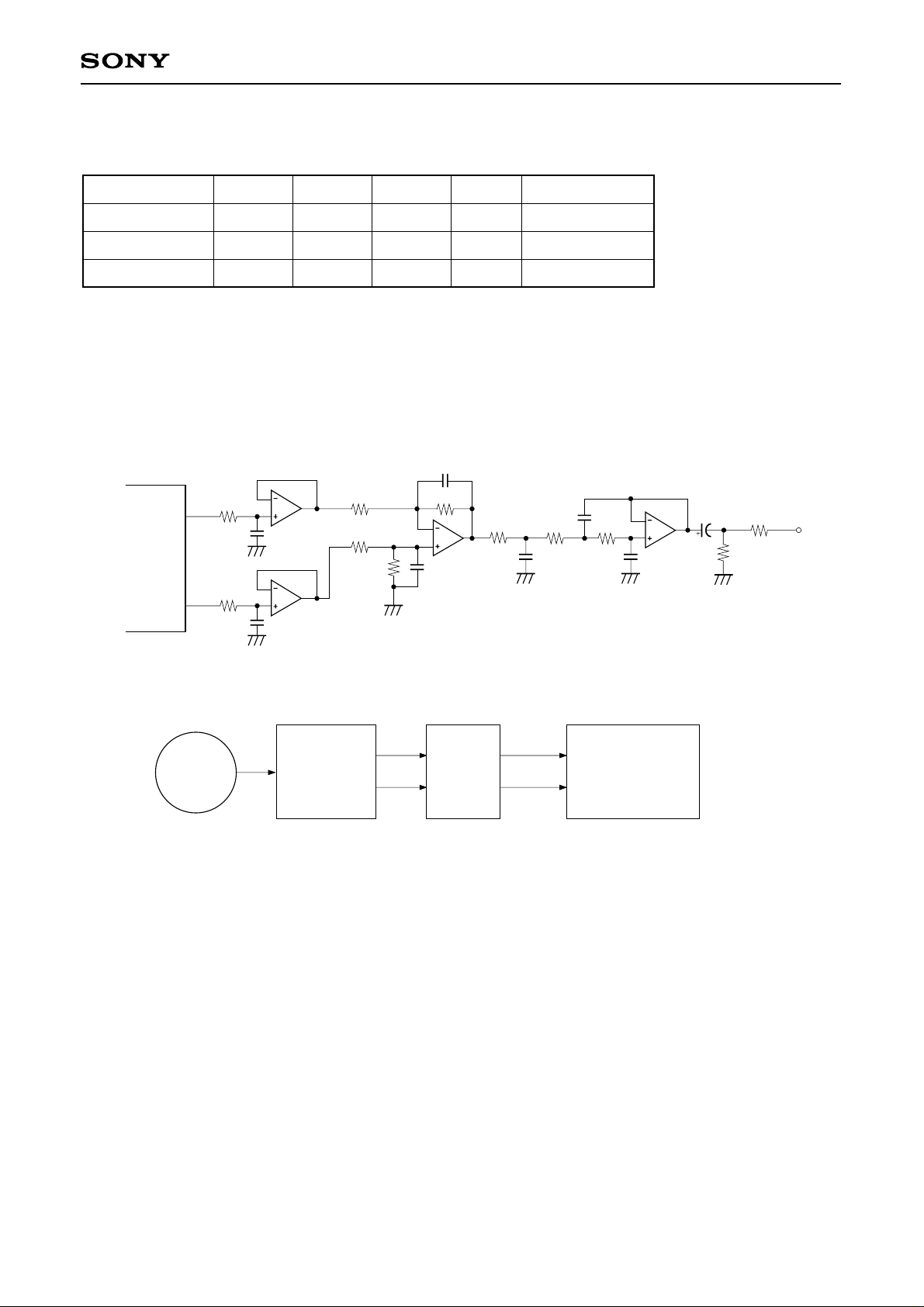
Internal 1-bit DAC analog characteristics
(fs = 48kHz, VDD = 5.0V, Ta = 25°C, signal frequency = 1kHz, measurement band = 4Hz to 20kHz, B mode)
Item
S/N
THD + N
Output level
∗1
"A" characteristic weighting filter used
∗2
When master clock is 256fs
Min. Typ. Max. Unit Remarks
90
0.011
1.95
dB
%
V(rms)
(EIAJ)
(EIAJ)
∗2
The following circuit is used for analog characteristics measurement.
CXD2027Q/R
LNO (RNO)
LPO (RPO)
130k
130k
47p
47p
5.4k
5.4k
4.7k
820p
4.7k
820p
4.7k
1800p
∗1
0.015
4.7k 4.7k
820p
22
12k
100
OUTPUT
TEST DISC CXD2027Q/R
DATA
Lch ANALOG
Rch
ANALOG
CIRCUIT
ANALOG TESTER
(ADVANTEST T7342)
– 15 –
Page 16

CXD2027Q/R
Description of Functions
• ALC
This detects the fluctuation of the input QPSK modulated signal level and absorbs the fluctuation by
controlling A/D VRT. With this function, a signal is output from ALCO after PWM modulation, and should be
fed back to the RT pin after integration.
• Carrier regeneration
A 5.727272MHz carrier is regenerated.
The input QPSK modulated signal is A/D converted at a sample rate of 22.909088MHz (5.727272MHz × 4),
and control voltage is generated using that sampling position as phase error data. The control voltage is
output from the PHAA pin after PWM modulation, and controls VCXO, which consists of an internal
oscillation cell and external crystal.
• Clock regeneration
This is a PLL circuit with 24.576MHz clock. It is 512 × fs, for use with the DAC.
Phase comparison is carried out using the regenerated I and Q signals and VCXO divided output, and
control voltage is generated. After PWM modulation, the control voltage is output from the PHAB pin, and
controls VCXO, which consists of an internal oscillation cell and external crystal.
• Data regeneration
A 2.048MHz bit stream is regenerated from the regenerated I and Q signals.
• Frame sync and master frame sync
Correlated detection and competitive counter format is used for sync protection. The number of rear
protection is set at three times, and that of front protection is set at 3, 5, 7, or 9 times.
Also, synchronizing to the master frame can be done when the master frame signal is being sent to the
control sign 14th bit. In this case, the number of rear protection is set to 2 times, and that of front protection
is set at 7, 9 or 11 times.
• Descramble
A superimposed PN signal is removed for BS.
Also, there is a built-in interface for an external descrambler unit.
• De-interleave
The data interleaved by the built-in 4kbit SRAM is returned to the correct data array.
• (63, 56) BCH sign error correction
This performs (63, 56) BCH sign error correction. Error capability is 1 error correction, 2 errors detection.
• Range bit BCH sign error correction
This performs (7, 3) BCH sign error correction. Error capability is 1 error correction, 2 errors detection.
When there are 2 errors, the previous value is held.
– 16 –
Page 17

CXD2027Q/R
• Control sign integration detection and 8th range bit integration detection
Integration detection is carried out in units of 15 frames. When a match of 12/15 or more is obtained, a
defined control sign is detected. However, updating is every 18 frames.
When a match of 12/15 or more is not obtained, the previous value is held.
Further, synchronizing to the master frame can be done when the master frame signal is being sent to the
control sign 14th bit.
After integration detection, the control sign and range bit can be read by the I2C bus.
• 10 → 14 bit data expansion
During A mode, the instantaneously compressed 10 bits of audio data are expanded to 14 bits according to
the range expansion rule. The lower bits of data are fixed at a set value during expansion, and the data is
treated as 16 bits.
• Upper bit majority detection
During B mode, this carries out upper bit majority detection and protects the upper bits.
• Mute signal generation
This performs muting by the external MUTE signal and internal logic, and also generates a mute signal
according to the mute setting from the I2C bus.
• Audio data interpolation
This receives the bit error detection signal and interpolation indication signal from majority detection, and
then carries out the average value interpolation or the previous value hold.
• Clock generation for D/A converter
This generates the clock for the DAC.
• Digital filter (DF) and de-emphasis
A 2ch 1-bit DAC with 2nd-order ∆∑ format noise shaper of quadruple oversampling filter is built in.
The output format is differential.
De-emphasis function corresponding to the mode is also built in.
• Audio interface
One of the following three output formats can be selected.
1) SONY: bit clock 32 fs/ MSB first/ 16 bits (for built-in D/A converter)
2) IIS: SONY format 1 BCLK delay
3) Bit clock 64fs / MSB first / 16 bits rearward truncation
• Digital interface
Conforms to the following digital audio interface format: type II form I (for consumer digital audio equipment)
•I2C bus interface
Control by microcomputer is carried out by the I2C bus I/F.
The slave address can be switched by controlling SASL; for low: D4, for high: D6.
– 17 –
Page 18

CXD2027Q/R
• Output channel selection
The output channels provided are analog output for built-in D/A converter Lch/Rch, one output system for
external D/A audio output and one for digital audio output. Channel selection can be done easily through
the I2C bus.
Unused channels can be suppressed using the I2C bus.
• Audio output selection
Mode selection can be carried out via the I2C bus.
• Zero cross muting
The I2C bus can be used for zero cross muting.
When a mute signal is input, muting is not carried out until zero cross conditions are satisfied for 1 frame.
If these conditions are not met for 1 frame, muting is forced at the next frame.
Zero cross mute cancel is performed in frame units.
The conditions for zero cross are a change in audio data MSB, or when audio data value is between 00ffh
and ff00h.
• Description of mute function
A signal is treated as a mute signal in the following cases:
1) when asynchronous
2) control sign 7th bit (non-broadcast flag) or 16th bit (audio suppression flag) is high
3) 8th range bit (audio chargeable flag) is high (however, only channel for high)
4) number of double error flags goes over a certain TH level (error frequency detection mute)
5) audio carrier (5.7272MHz) can not be detected
6) an I2C bus mute flag is up
7) for other than audio
1. Asynchronous flag mute
Muting is applied when an asynchronous state exists. Also, the number of front sync protection can be
changed among 3, 5, 7 or 9 times by the I2C bus, so the conditions for asynchronous flag muting can be
changed.
2. Muting by control sign 7th and 16th bits
The control sign 7th bit is a flag indicating broadcast or non-broadcast. If this bit is high, muting is
applied. Also, the I2C bus can be used so that this bit does not apply muting.
The control sign 16th bit audio suppression flag is used when broadcast channels are switched and
when transmission modes are switched. Both use the value after integration detection.
3. Chargeable flag detection mute
The 8th range bit indicates if audio data is for a chargeable broadcast or not. For a chargeable
broadcast, a flag ("H") goes up in that bit's position. When this bit is high, the broadcast is detected as
chargeable and muting is applied. Further, the I2C bus can be used for each channel so that this bit
does not apply muting. The value after every 18 frames of integration detection is used.
– 18 –
Page 19

CXD2027Q/R
4. Error frequency detection mute
Muting is applied after BCH (63, 56) sign error correction is executed for every 64 data, when the
number of double error detection flags goes over a certain TH (threshold value) level during a certain
number of frames. Also, the I2C bus can be used so that muting is not applied. The setting values are
indicated below.
Number of frames: 128, 256, 512, 1024
Up to 32 double errors can be detected in one frame, so 1/16, 1/8, 1/4 and 1/2 of the maximum
detections for each frame number are set as the TH levels.
Therefore, there are 16 possible combinations, and the value is set by the I2C bus.
The TH level for muting cancel is half of the TH value when muting is applied; in other words, 1/32, 1/16,
1/8 and 1/4, respectively.
5. Carrier detection mute
When the BS broadcast audio carrier frequency of 5.7272MHz can not be detected by the PSK
demodulator unit, muting is applied. Also, the I2C bus can be used so that muting is not applied.
6. I2C bus muting
The I2C bus can apply forced muting to analog and AUD outputs. TX output is locked to analog output.
7. Muting other than audio
Muting is done for other than audio mode when the control sign 2nd and 3rd, or 4th and 5th bits are "H, H".
– 19 –
Page 20

External descramble I/F circuit example
COATEC and SkyPort units can be connected simultaneously.
CXD2027Q/R
CXD2027Q/R
BITO
BSTMI
COATEC unit SkyPort unit
DSLA
0
0
1
1
∗
The COATEC unit and SkyPort unit can be connected simultaneously.
DSLB
0
1
0
1
BITI
BSTMO
Unit connection
DSLB
RGND
Descramble format
COATEC, SkyPort
SkyPort
COATEC
Internal
DATI
∗
DATO
DATB
DSDO
DASLC
DATA
DATI
2
C BUS
I
register
DATO
DSLA
DASL
However, use the I2C bus to set DASLC at high when turning off the COATEC unit power supply.
– 20 –
Page 21
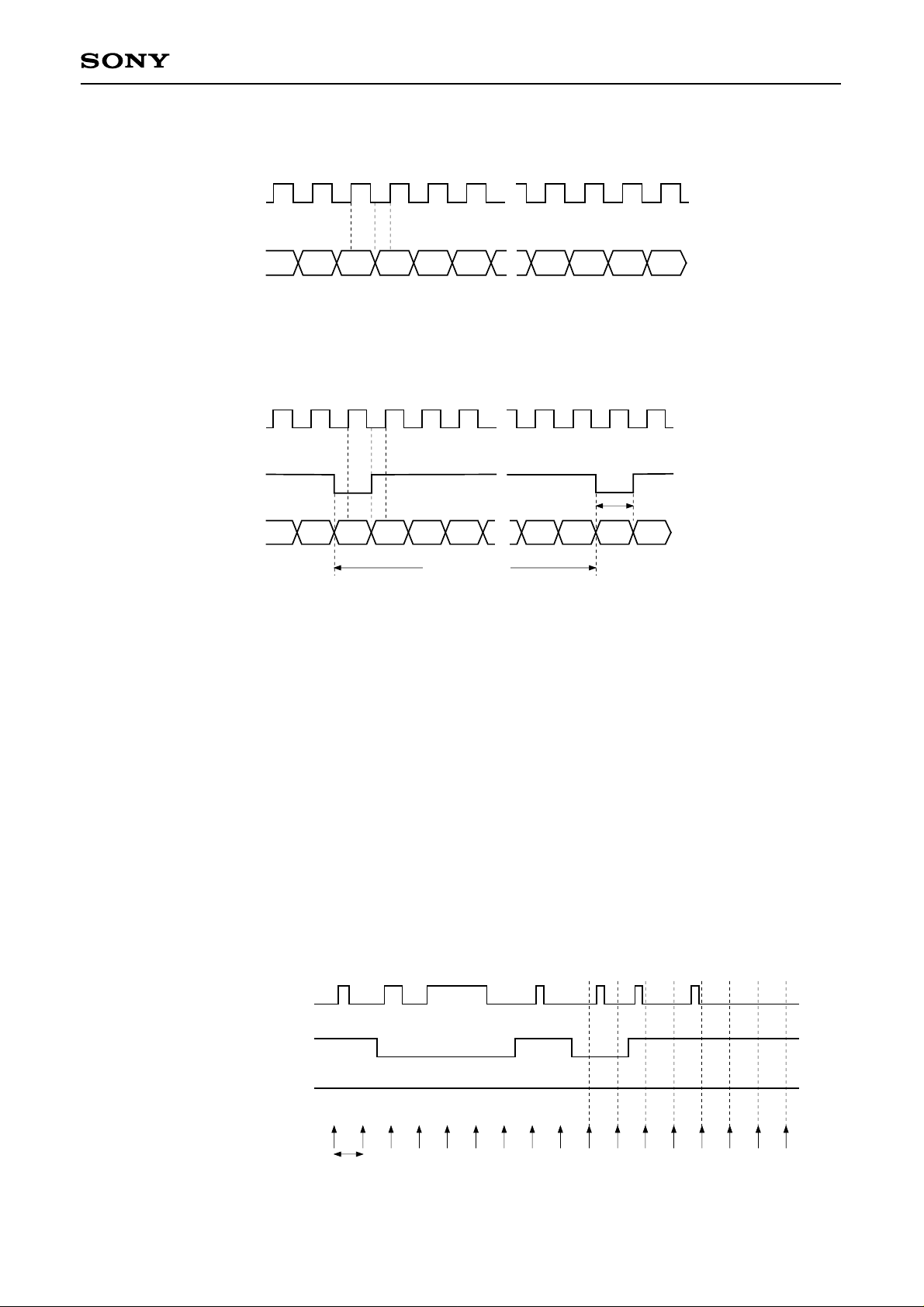
Bit stream signal interface
CK2M
CXD2027Q/R
BITO is output at falling sync.
BITO
2048 1 2 3 4 2047 2048 1 2
Data interface after BCH error correction
CK2M
FRAM
DATO is output at falling sync.
DATO
2048 1 2 3 4 2047 2048 1 2
1ms
1 frame
Examples of error detection countermeasures for low C/N control sign and chargeable flag integration
detection
When C/N is low, NSYN frequently goes high level (asynchronous state).
In this case, problems such as wrong display or wrong detection of control sign 7th bit "broadcast/nonbroadcast" flag may occur due to incorrect integration detection. This can be improved using the
microcomputer software shown below.
Integration detection result can be updated only when NSYN is low level. Detection results of this IC are read
by the standard trigger of the microcomputer, and if the result values match for 5 to 6 times continuously, the
detection result is taken as an update for the system. It is also possible to update the integration detection
result by the continuous matching of 7 times or more. However, standard trigger cycle of the microcomputer
must be set about 18ms.
NSYN
Control sign,Chargeable flag
(IC)
Control sign,Chargeable flag
(microcomputer)
→ integration detection results
Standard trigger
(microcomputer)
18ms
123456
– 21 –
Page 22

CXD2027Q/R
Description of I2C bus
The I2C bus is a bidirectional serial bus system developed by Philips. It can transmit and receive data
between multiple devices using two lines, SCLK (Serial Clock) and SDA (Serial Data).
This LSI has a built-in I2C bus interface circuit and is compatible with slave RECEIVER and slave
TRANSMITTER operation modes.
For the transfer configuration, both RECEIVER mode and TRANSMITTER mode have sub-addresses.
RECEIVER mode
The first byte is the slave address, the second byte is the sub-address, and data is read at the third byte
and after. Continuous data reading is also possible. After transmission of the first byte, the sub-address
is made (+1) automatically.
TRANSMITTER mode
The first byte is the slave address, and data is sent at the second byte and after. Continuous data output
is also possible. After transmission of the first byte, the sub-address is made (+1) automatically.
When there is no verification answer from the master, the SDA line is released.
To read data, the sub-address for the data to be read is written in RECEIVER mode, then the data is read
in TRANSMITTER mode.
The SDA line is released for initial reset, so the bus is not occupied. Also, even if the IC supply voltage falls
to 0V, the bus is not occupied. Nonetheless, please keep within the absolute maximum ratings.
This bus is compatible not only with standard mode (maximum 100kbit/s) but with high speed mode
(maximum 400kbit/s) as well.
– 22 –
Page 23
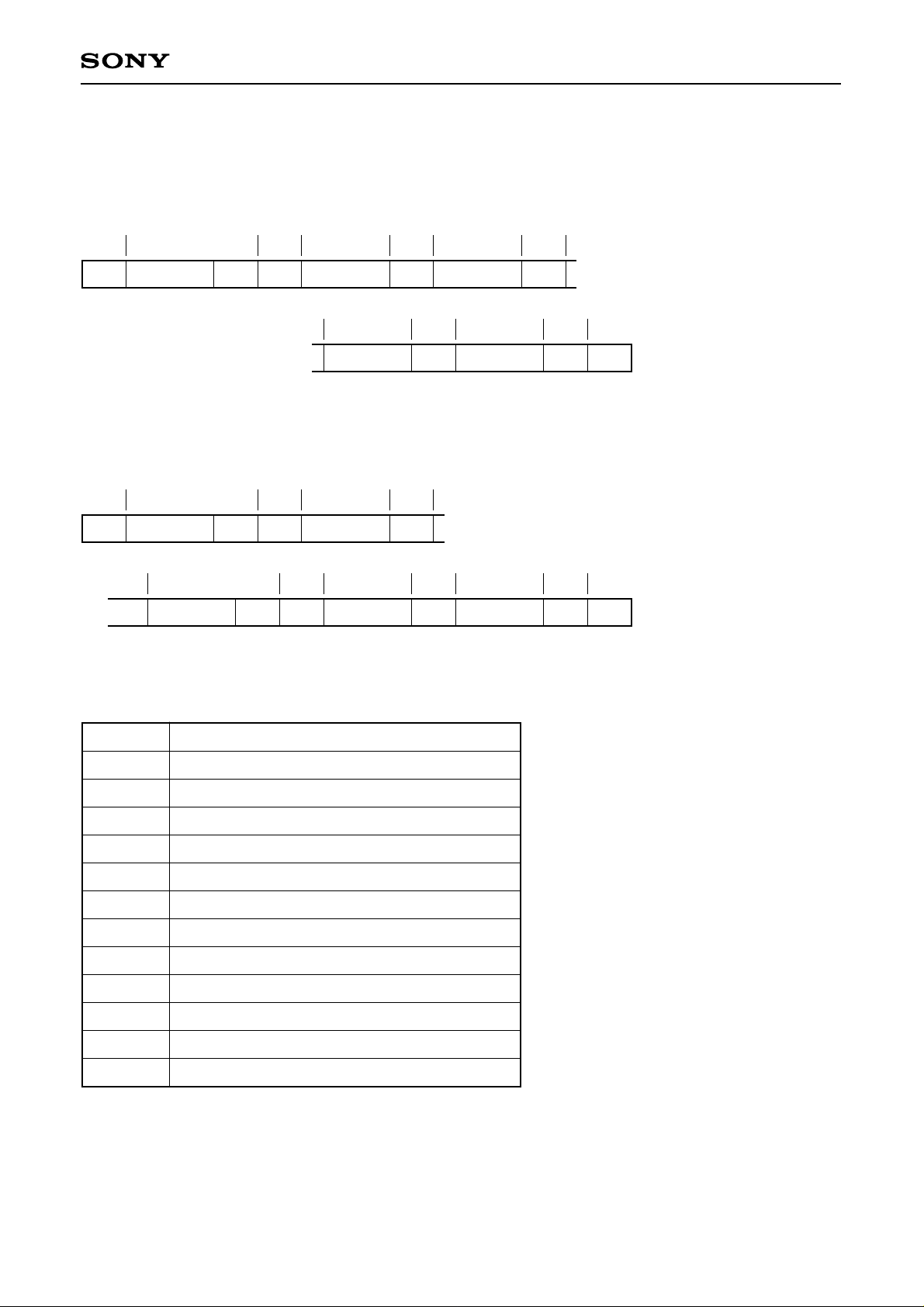
• Specifications
Data write (RECEIVER mode)
CXD2027Q/R
7654321
0 76543210 1 76543210 11
SLAm Wm SUBm As DATAm AsAsSm
76543210 1 176543210
to
DATAm As DATAm As P
Data read (RECEIVER mode & TRANSMITTER mode)
7654321
0 76543210 11
SLAm Wm SUBm AsAsSm
765432107654321 110187654321
to
DATAsSLAm AmAsRmSrm DATAs XAm P
to
to
Symbol
∗
m
∗
s
S
Sr
P
SLA
SUB
DATA
W
R
A
XA
Description
from master to slave
from slave to master
Start Condition
Start Condition
Stop Condition
Slave Address
Sub Address
Data
0 : Write Master → Slave
1 : Read Slave → Master
Clock pulse for Acknowledgement (SDA: L)
Acknowledgement none (SDA:H)
– 23 –
Page 24
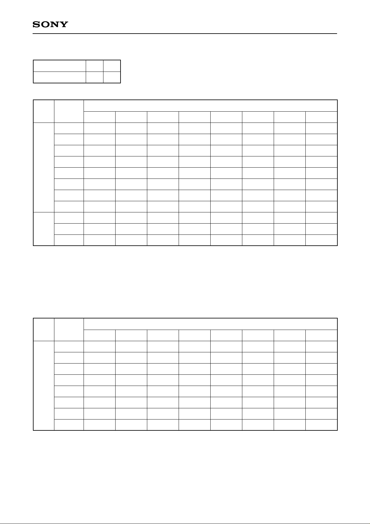
I2C bus control table
CXD2027Q/R
SASL
Slave address
R/W
Sub-
address
00'H
01'H
02'H
03'H
WR
04'H
05'H
06'H
07'H
00'H
RD
01'H
02'H
L
D4HD6
MSB
Data LSB
bit7 bit6 bit5 bit4 bit3 bit2 bit1 bit0
A1S1
BUSMT1
OTSTP1
DASLC
(TSB0)
RGOF1
CC1
CC9
(L)
A1S2
BUSMT2
OTSTP2
C1SL
(TSB1)
RGOF2
CC2
CC10
(L)
A1S3
AMUTE
OTSTP3
LRSL
XEOFF
RGOF3
CC3
CC11
(L)
SIG
OTSTP4
IIS
XINH
RGOF4
CC4
CC12
(L)
A2S1
DOS1
MTOF0
NF1
BLFS
C2
PI1
OTSL
CC5
CC13
RG81
A2S2
DOS2
MTOF1
NF2
FPCC
C10
PI2
MFRAM
CC6
CC14
RG82
A2S3
DOS3
MTOF2
TH1
FPCB
XPRT
NR
(TEST2)
CC7
CC15
RG83
MTOF3
TH2
(TEST1)
DOMU
(TEST3)
CC8
CC16
RG84
Blanks : Data not related to internal logic.
( ) : Data for testing. Fix to the default value.
(L) : Low is output.
MSB, LSB : Data is transmitted with MSB first.
Default data (default value of internal register after master reset)
W
Sub-
address
00'H
01'H
02'H
03'H
MSB
bit7 bit6 bit5 bit4 bit3 bit2 bit1 bit0
0
—
0
0
1
—
0
0
0
—
1
0
Data LSB
—
—
0
0
WR
04'H
05'H
06'H
07'H
0
—
(0)
1
0
—
(0)
1
—
0
0
—
1
1
0
1
0
0
1
0
1
1
0
0
1
1
1
1
0
1
0
0
0
0
1
0
1
0
0
(0)
—
—
1
1
(0)
0
—
(0)
( ) : Always fix to the default value.
– 24 –
Page 25

• BUS setting values for audio output selection
Sub-address 00'H 00000000'B
CXD2027Q/R
BIT No.
bit7
bit6
bit5
bit3
bit2
bit1
stereo
Name Description
A1S1
A1S2
Audio output mode selection when using built-in DF/DAC
A1S3
A2S1
A2S2
Audio output mode selection when using external DF/DAC
A2S3
A1S1
Applications
A2S1
DOS1
TV
0
A mode
B mode
TV
independent
main + sub
main
1
X
0
0
A1S2
A2S2
DOS2
X
X
X
1
0
A1S3
A2S3
DOS3
X
X
X
X
0
A mode
2ch mono
independent
B mode
TV
A mode
1ch mono
independent
B mode
Sub-address 01'H 00000001'B
BIT No.
bit3
bit2
Name Description
DOS1
DOS2
Output mode selection when using digital interface
sub
main + sub
main
sub
main + sub
main
sub
main
main
main
0
1
1
1
X
X
X
0
1
X
0
1
0
0
1
0
0
X
X
X
1
X
0
1
X
0
1
X
X
X
bit1
DOS3
Same setting method as for A1S1, A1S2 and A1S3
– 25 –
Page 26

• Muting-related BUS setting values
Sub-address 02'H 00000010'B
CXD2027Q/R
BIT No.
bit7
bit6
bit3
bit2
bit1
bit0
Name Description H L
BUSMT1
BUSMT2
MTOF0
MTOF1
MTOF2
MTOF3
Audio data mute when using built-in DF/DAC
Audio data mute when using external DF/DAC
Carrier detection mute
Non-broadcast flag mute
Error occurrence frequency mute
External mute (EXMU)
Sub-address 03'H 00000011'B
BIT No.
bit7
bit6
bit5
bit4
Name Description H L
OTSTP1
OTSTP2
OTSTP3
OTSTP4
Signal suppression for external DF/DAC (AUD, LRCK, BCLK)
Signal suppression for external descramble
(CK2M, FRAM, DATO)
Control sign output suppression (NSYN, CCUP, CC1)
Built-in DF/DAC operation / non-operation selection
ON
ON
ON
ON
ON
ON
Non-
operation
Non-
operation
Non-
operation
Non-
operation
OFF
OFF
OFF
OFF
OFF
OFF
Operation
Operation
Operation
Operation
bit3
bit2
bit1
bit0
bit3
NF1
0
0
1
1
bit1
TH1
0
0
1
NF1
NF2
TH1
TH2
NF2
TH2
bit2
0
1
0
1
bit0
0
1
0
Error occurrence frequency mute setting (number of frames)
Error occurrence frequency mute setting (threshold value)
Number of frames
128
256
512
1024
Threshold value
MUTE
1/2
1/4
1/8
∗1
Cancel
∗2
1/4
1/8
1/16
1
∗1
MUTE when over this value
∗2
MUTE cancel when below this value
1
1/16
1/32
– 26 –
Page 27
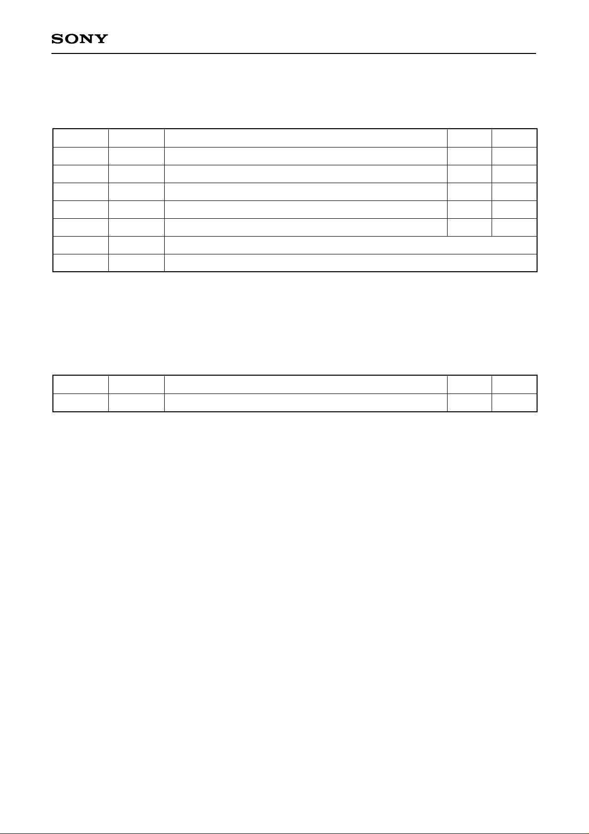
• BUS setting values for chargeable flag mute
Sub-address 07'H 00000111'B
CXD2027Q/R
BIT No.
bit7
bit6
bit5
bit4
bit2
bit1
bit0
Name Description H L
RGOF1
RGOF2
RGOF3
RGOF4
MFRAM
TEST2
TEST3
Audio 1ch mute
Audio 2ch mute
Audio 3ch mute
Audio 4ch mute
Master frame sync processing
For testing (fix to low)
For testing (fix to low)
ON
ON
ON
ON
OFF
• BUS setting values for external I/F, etc.
Sub-address 02'H 00000010'B
BIT No.
Name Description H L
bit4 SIG Signal polarity selection for external descramble I/F Inverted Positive
Corresponding input pins : BITI, DATA, DATB
Corresponding output pins: CK2M, DATO, FRAM
OFF
OFF
OFF
OFF
ON
– 27 –
Page 28
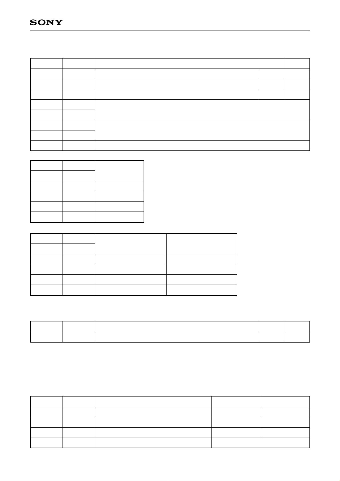
Sub-address 04'H 00000100'B
CXD2027Q/R
BIT No.
bit7
bit6
bit5
bit4
bit3
bit2
bit1
bit0
bit4
IIS
1
1
0
0
Name Description H L
DASLC
C1SL
LRSL
External descramble I/F control
CC1 (control sign 1st bit) output polarity inversion
LRCK polarity inversion
Refer to page 20.
Inverted
Inverted
IIS
Audio output format switching
BLFS
FPCC
FPCB
TEST1
Selection of the number of front protection for frame sync protection and master
frame syncprotection selection
For testing (fix to low)
bit3
Format
BLFS
1
0
1
0
Prohibited
2) IIS
3) 64fs
1) SONY
Positive
Positive
bit2
FPCC
1
1
0
0
bit1
FPCB
1
0
1
0
The number of frame sync
front protection
3
5
7
9
The number of master
frame sync front protection
7
9
11
11
Sub-address 07'H 00000111'B
BIT No.
Name Description H L
bit3 OTSL DTUP pin output signal switching DED CCUP
• Digital I/F BUS setting values
Sub-address 05'H 00000101'B
BIT No.
Name Description H L
bit3
bit2
bit1
bit0
C2
C10
XPRT
DOMU
Digital copy allowed/prohibited selection
Channel status 10th bit
Parity inversion selection for digital interface
Mute for digital interface (TX is DC low)
– 28 –
Allowed
General
Transmission error
ON
Prohibited
BS
Normal
OFF
Page 29
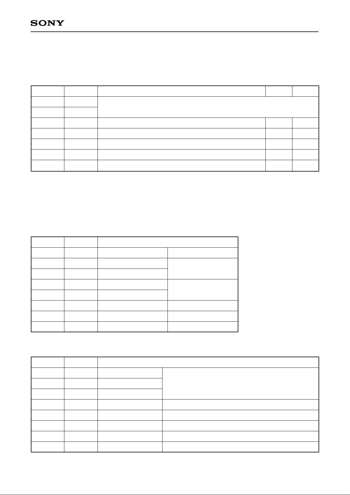
• DF and D/A converter-related BUS setting values
Write register
Sub-address 06'H 00000110'B
CXD2027Q/R
BIT No.
bit7
Name Description H L
TSB0
For testing (normally set to low regardless of input data)
bit6
bit5
bit4
bit3
bit2
bit1
TSB1
XEOFF
XINH
PI1
PI2
NR
Digital de-emphasis selection
DC dither selection
DC dither phase control Rch
DC dither phase control Lch
Modulation NR
• Control sign bit reading after integration correction
Sub-address 00'H 00010000'B
BIT No.
bit7
Name Description
CC1
Control sign 1st bit
Mode selection
ON
ON
Inverted
Inverted
ON
OFF
OFF
Positive
Positive
OFF
bit6
bit5
bit4
bit3
bit2
bit1
bit0
CC2
CC3
CC4
CC5
CC6
CC7
CC8
Control sign 2nd bit
Control sign 3rd bit
Control sign 4th bit
Control sign 5th bit
Control sign 6th bit
Control sign 7th bit
Control sign 8th bit
Sub-address 01'H 00010001'B
BIT No.
bit7
bit6
bit5
bit4
bit3
bit2
Name Description
CC9
CC10
CC11
CC12
CC13
CC14
Control sign 9th bit
Control sign 10th bit
Control sign 11th bit
Control sign 12th bit
Control sign 13th bit
Control sign 14th bit
TV audio
Additional audio
Suppression backup
Broadcast identification
Expansion bit
Expansion bits
Video scramble existent/non-existent
—
Master frame sync flag H: asynchronous, L: synchronous
bit1
bit0
CC15
CC16
Control sign 15th bit
Control sign 16th bit
Data suppression
Audio output suppression
– 29 –
Page 30
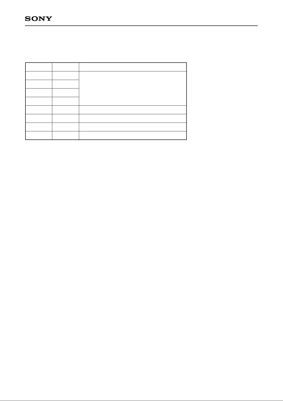
• Range 8th bit read after integration correction
Sub-address 02'H 00010010'B
CXD2027Q/R
BIT No.
bit7
bit6
bit5
bit4
bit3
bit2
bit1
bit0
Name Description
—
—
Low level fixed output
—
—
RG81
RG82
RG83
RG84
Range 8th bit (chargeable flag) 1ch
Range 8th bit (chargeable flag) 2ch
Range 8th bit (chargeable flag) 3ch
Range 8th bit (chargeable flag) 4ch
– 30 –
Page 31
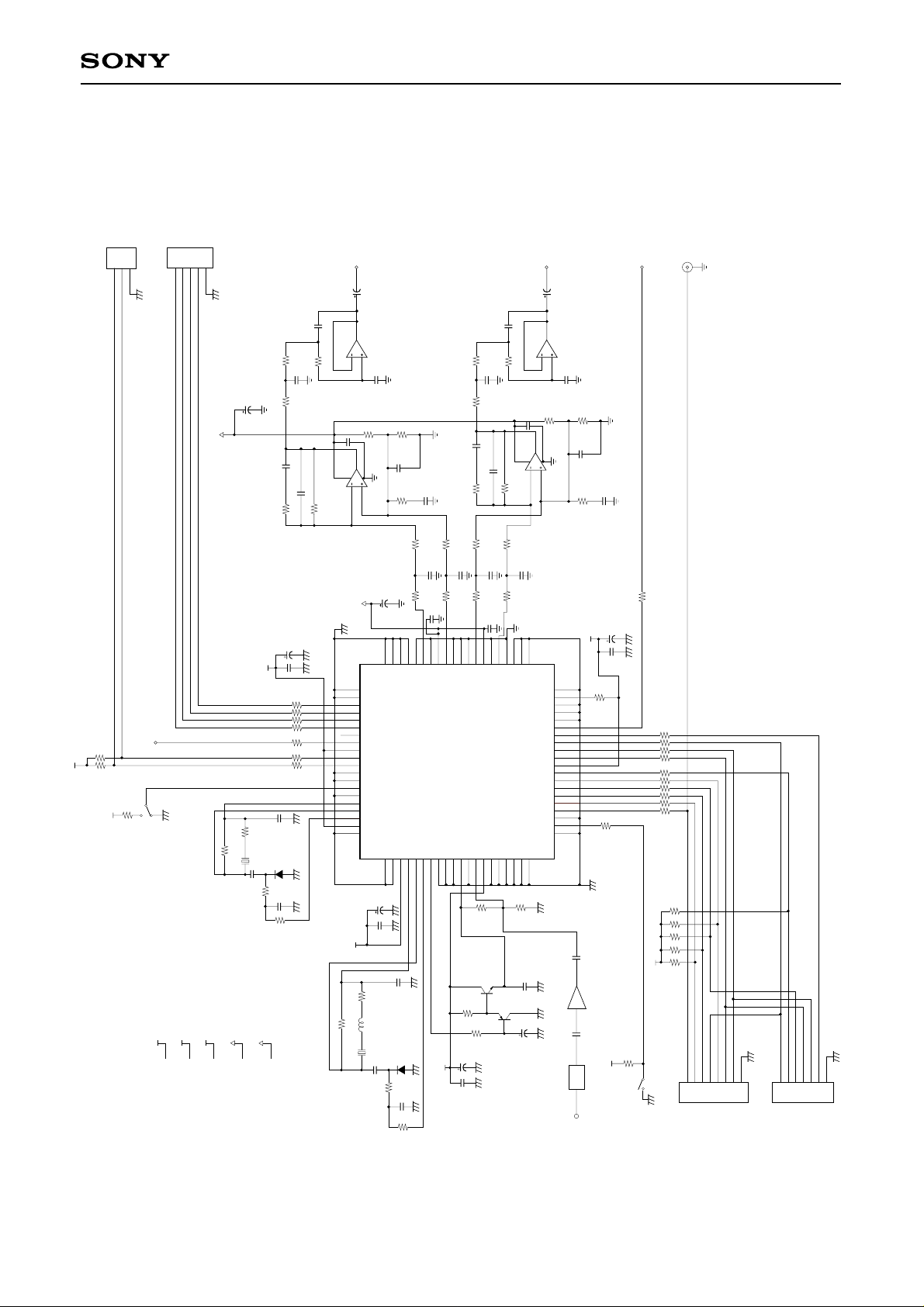
CXD2027Q/R
D24 + 5V
1
SCL2SDA
4.7k
4.7k
D24 + 5V
C
2
I
3
5.6k
NSYN
Dad + 5V
1F256
2BCLK
D23 + 5V
D_out
3LRCK
4AUD
5
D24 + 5V
0.1µ
Aout + 12V
100k
A + 5V
47µ/16V
D24 + 5V
330
24MHz
1800p: CH
0.047µ/16V
Aout + 12V
10p: CH
22k
4.7k
: CH
0.01µ
680 680
2200p: CH
150p: CH
6.8k
47µ/16V
100
× 5
× 2
220
HVU359TRF
0.1µ
0.027µ
680
0.1µ
15k
R ch
Output
47µ/16V
7
NJM4580E
6
5
1500p: CH
30k
30k
150p
8
1
2
41
42
43
44
45
46
47
48
49
50
51
52
53
54
55
56
57
58
59
60
D23 + 5V
100k
: CH
4
2200p: CH
6.8k
3
NJM4580E
120p: CH
47µ/16V
9.1k 8.2k
39
62
0.1µ
NC6
SASL
DD5
NC11
V
12p: CH
22k
0.01µ
4.7k
0.1µ
SS6VSS5
NC5
RNO
V
M23O
M23I
PHAA
ALCO
HVU359TRF
A + 5V
40383736353433323130292827262524232221
NC7
NC8
TST6
AUD
LRCK
BCLK
F256
DTUP
NSYN
DD
3
V
SDA
SCLK
SS7
V
TST8
MUTE
SS
8
V
MCKO
MDKI
PHAB
DD4
V
NC9
NC10
61636465666768697071727374757677787980
47µ
16V
68
2.7µ
23MHz
390p: CH
9.1k 8.2k
SS4
DD2
RPO
V
V
CXD2027R
SS9
NC12
TST7RTNC13
V
Dad + 5V
120p: CH
SS3
LPO
V
TST1
ADIN
3
5.6k
22k
47µ
16V
0.1µ
: CH
0.01µ
680 680
150p: CH
2200p: CH
6.8k
120p: CH
9.1k 8.2k
0.1µ
DD1
NC4
LNO
V
ADVD
ADVSRBGR
12k
FE ≥ 200)
2SC2712
(h
1
2
1
2
0.027µ
680
8
15k
120p: CH
9.1k 8.2k
SS2VSS1
NC3
V
TST0
NC14
12k
3
2SA1162
0.1µ
2
NC2
NC15
2200p
47µ/16V
L ch
Output
47µ/16V
7
NJM4580E
6
5
1500p: CH
30k
30k
1
150p:
CH
4
3
NC1
TST5
TST4
TST3
TST2
TX
CC1
DATO
FRAM
CK2M
DD
0
V
DATA
DATB
DSLA
DSLB
BITI
BITO
SS
0
V
MRST
NC0
6.8k
NJM4580E
D24 + 5V
20
19
18
17
16
15
14
13
12
11
10
9
8
7
6
5
4
3
2
1
0.01µ
Buffer
1000p
BPF
INPUT
ANALOG
2200p: CH
47µ/16V
0.01µ
5.6k
100
10k
D24 + 5V
TX
100
D24 + 5V
SW
REST
BITO
The analog de-emphasis circuit is included in the external circuit connected to the built-in
DAC.
Note 1) Circuit connection and constants are the same for the CXD2027Q.
Note 2) This circuit example shows digital de-emphasis off.
100
× 4
× 6
100
5.6k
× 5
8 BITO
7 BITI
6 DSLB
5 DATO
4 DATB
3 CK2M
2 FRAM17 DATO
COATEC
6 DATA
Application circuits shown are typical examples illustrating the operation of the devices. Sony cannot assume responsibility for
any problems arising out of the use of these circuits or for any infringement of third party patent and other right due to the same.
5 DSLA
4 CK2M
3 FRAM
2 CC1
1
SkyPort
Application Circuit
– 31 –
Page 32
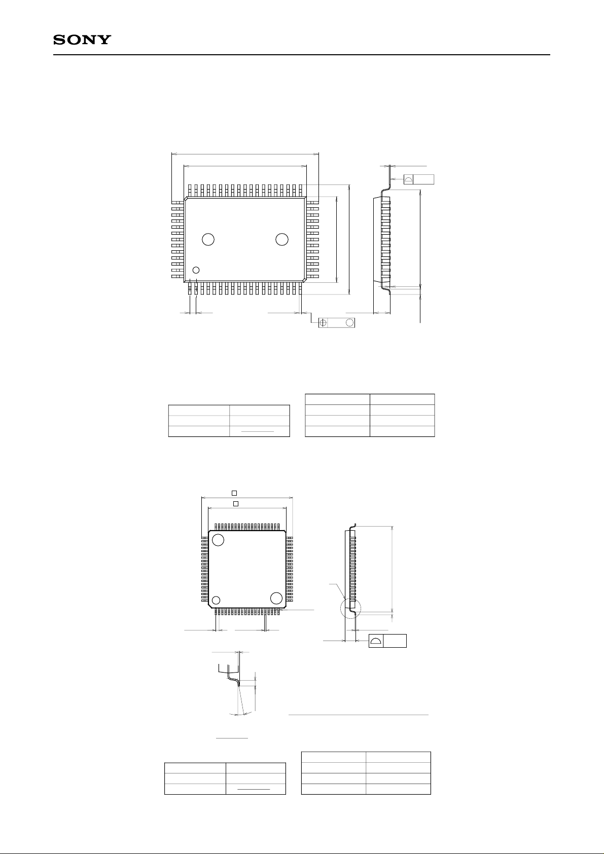
Package Outline Unit: mm
CXD2027Q/R
CXD2027Q
52
64
SONY CODE
EIAJ CODE
JEDEC CODE
64PIN QFP(PLASTIC)
23.9 ± 0.4
+ 0.4
20.0 – 0.1
51
1
1.0
+ 0.15
0.4 – 0.1
33
32
+ 0.4
14.0 – 0.1
17.9 ± 0.4
20
19
± 0.12
+ 0.35
2.75 – 0.15
M
PACKAGE STRUCTURE
QFP–64P–L01
∗
QFP064–P–1420
PACKAGE MATERIAL
LEAD TREATMENT
LEAD MATERIAL
PACKAGE WEIGHT
EPOXY RESIN
SOLDER/PALLADIUM
COPPER /42 ALLOY
1.5g
0.15 – 0.05
+ 0.2
0.1 – 0.05
PLATING
+ 0.1
0.15
16.3
0.8 ± 0.2
CXD2027R
61
80
0.5 ± 0.08
SONY CODE
EIAJ CODE
JEDEC CODE
60
1
0.1 ± 0.1
0° to 10°
DETAIL A
80PIN LQFP (PLASTIC)
14.0 ± 0.2
∗ 12.0 ± 0.1
41
20
+ 0.08
0.18 – 0.03
0.5 ± 0.2
LQFP-80P-L01
∗QFP080-P-1212-A
40
+ 0.05
0.127 – 0.02
(13.0)
0.5 ± 0.2
0.1
21
(0.22)
A
+ 0.2
1.5 – 0.1
NOTE: Dimension “∗” does not include mold protrusion.
PACKAGE STRUCTURE
PACKAGE MATERIAL
LEAD TREATMENT
LEAD MATERIAL
PACKAGE WEIGHT
EPOXY / PHENOL RESIN
SOLDER PLATING
42 ALLOY
0.5g
– 32 –
 Loading...