

Page 1

IEEE1394 Link Layer LSI for DVB and DSS
For the availability of this product, please contact the sales office.
Description
The CXD1948R is a Link Layer LSI conforming to
the IEEE1394 serial bus standard. During transmission,
the MPEG2 transport stream is time stamped,
transformed to IEEE1394 format and sent to the
IEEE1394 Phy IC.
During reception, the signal from IEEE1394 is kept
in the built-in FIFO, synchronized to the time stamp
value and output.
This IC utilizes Apple Computer’s Fire Wire
technology.
Features
• Conforms to IEEE1394 serial bus standard
• Supports DVB and DSS transport streams
• Dedicated ports for asynchronous data/isochronous
data
• Isochronous data inserted from asynchronous data
port
• Smoothing buffer function
• Large capacity FIFO
Isochronous transmit/receive FIFO 960 × 32 bits
Asynchronous transmit FIFO 30 × 33 bits
Asynchronous receive FIFO 36 × 33 bits
Isochronous Insert Packet Transmit Buffer
47 × 33 bits
• CIP header automatic attachment/detection
Absolute Maximum Ratings (Ta = 25°C)
• Supply voltage VDD Vss – 0.5 to +4.6 V
• Input voltage VI Vss – 0.5 to VDD + 0.5 V
• Output voltage VO Vss – 0.5 to VDD + 0.5 V
• Operating temperature
• Storage temperature
Recommended Operating Conditions
• Supply voltage VDD 3.0 to 3.6 V
• Operating temperature
CXD1948R
100 pin LQFP (Plastic)
Topr –20 to +75 °C
Tstg –55 to +150 °C
Topr –20 to +75 °C
Applications
• Digital interface for D-STB
• Digital interface for D-VHS
Structure
Silicon gate CMOS IC
Fire Wire is a registered trademark of Apple Computer Corporation, USA
Sony reserves the right to change products and specifications without prior notice. This information does not convey any license by
any implication or otherwise under any patents or other right. Application circuits shown, if any, are typical examples illustrating the
operation of the devices. Sony cannot assume responsibility for any problems arising out of the use of these circuits.
– 1 –
E96844-PS
Page 2

CXD1948R
Contents
1. Block Diagram ............................................................................................................................................... 3
2. Pin Configuration ........................................................................................................................................... 4
3. Pin Description .............................................................................................................................................. 5
4. Electrical Characteristics ............................................................................................................................... 8
4-1. DC Characteristics ................................................................................................................................ 8
4-2. AC Characteristics ................................................................................................................................ 8
4-3. Timing Definitions ................................................................................................................................. 8
5. Isochronous Communication ......................................................................................................................... 9
5-1. Built-in FIFO ......................................................................................................................................... 9
5-2. Transport Stream I/F .......................................................................................................................... 10
5-3. Transport Stream Packet Split and Combine Functions ..................................................................... 18
5-4. Transport Stream ................................................................................................................................ 19
5-5. Isochronous Packet Structure ............................................................................................................ 20
5-6. Relationship between Additional Data and CFR Registers ................................................................ 27
5-7. 27MHz Time Stamp ............................................................................................................................ 27
5-8. Dummy Packet Transmission ............................................................................................................. 28
5-9. Time Stamp ........................................................................................................................................ 29
5-10. Error Processing ............................................................................................................................... 30
5-11. Late Processing ................................................................................................................................ 31
6. Asynchronous Communication .................................................................................................................... 31
6-1. Host/IF ................................................................................................................................................ 31
6-2. CFR .................................................................................................................................................... 34
6-3. Asynchronous Packet Transmission .................................................................................................. 44
6-4. Asynchronous Packet Reception ........................................................................................................ 47
6-5. CXD1948R Data Format .................................................................................................................... 52
6-6. Self-ID Packet Receiving Error Processing ........................................................................................ 62
7. Insert Packet ............................................................................................................................................... 63
7-1. Insert Packet Transmission ................................................................................................................ 63
7-2. Adding a Time Stamp to the Insert Packet ......................................................................................... 66
8. Link-Phy Communication ............................................................................................................................ 67
8-1. Link-Phy Interface Specifications ....................................................................................................... 67
8-2. Communication ................................................................................................................................... 67
9. Parallel Input/Output Port ............................................................................................................................ 74
10. System Configuration Example ................................................................................................................. 75
Annex. Corresponding Table for CFR Access Address And Host Interface I/O Data ..................................... 76
– 2 –
Page 3
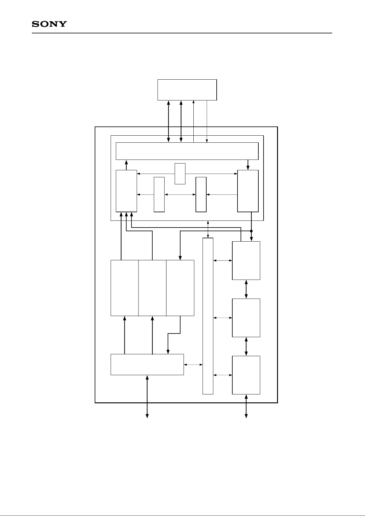
PHY
CXD1948R
Transmitter
FIFO
Transmit
Asynchronous
D [0 : 3]
Cycle Timer
Buffer
Transmit
Insert Packet
LREQ
CTL [0 : 1]
I/F
PHY
CRC
Buffer
Receive
Asynchronous
SYSCLK
Cycle Monitor
Receiver
Detect/
Generate
Header/Sync
Link Core
1. Block Diagram
Host
Host
I/F
– 3 –
Receive
Transmit/
Isochronous
Configuration Register
Transport
Data Stream
MPEG2
Transporter
FIFO
I/F
Page 4
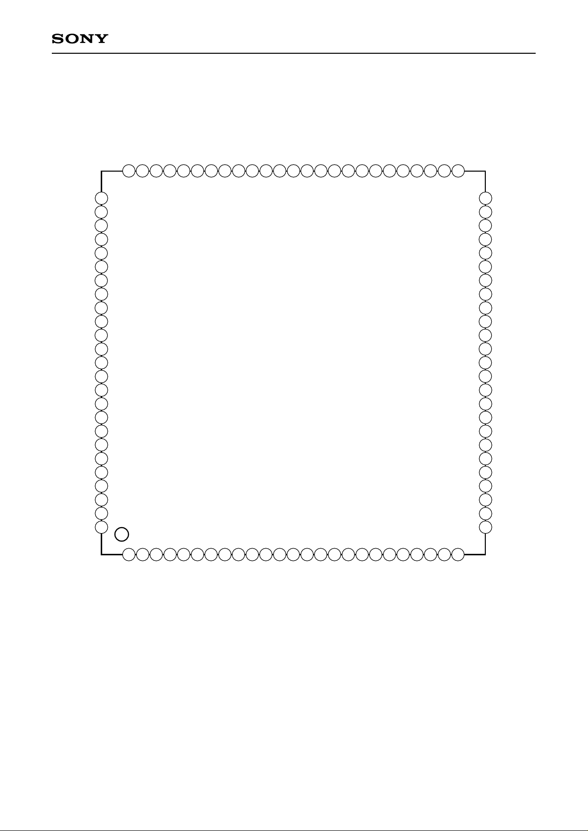
2. Pin Configuration
CXD1948R
VSS
AICK
IFFULL
IFEMPTY
PACKETEN
DD
V
CK27
IOEC
AIDT15
AIDT14
AIDT13
AIDT12
AIDT11
AIDT10
AIDT9
AIDT8
SS
V
AIDT7
AIDT6
AIDT5
AIDT4
AIDT3
AIDT2
AIDT1
AIDT0
76
77
78
79
80
81
82
83
84
85
86
87
88
89
90
91
92
93
94
95
96
97
98
99
100
AIREAD
75
AIWRITE
73
74
READREQ
PACKETGAP
ERRFLAG
72
71
PORT4
70
PORT3
69
TEST19
67
68
LPS
66
DD
V
65
LREQ
64
CTL0
63
CTL1
62
SS
D0
V
D1
60
59
61
D2
58
D3
57
TEST18
TEST17
55
56
TEST15
TEST16
53
54
SS
V
DD
SYSCLK
V
5152
50
TEST14
49
V
48
TEST13
47
TEST12
46
PORT2
45
PORT1
44
PORT0
43
TEST8
42
XINT
41
XW/R
40
XWAIT
39
XCS
38
V
37
ADDRESS0
36
ADDRESS1
35
ADDRESS2
34
ADDRESS3
33
ADDRESS4
32
ADDRESS5
31
ADDRESS6
X8/16
30
XRESET
29
V
28
TEST7
27
TEST6
26
SS
DD
SS
1
SS
V
2
3
DATA15
4
DATA13
DATA14
6
5
DATA12
7
DATA11
DATA10
8
DATA9
9
DATA8
10
DD
V
11
DATA7
12
DATA6
– 4 –
13
DATA5
14 15
DATA4
16
DATA2
DATA3
17
DATA1
18
DATA0
19
SS
V
20
TEST0
21
TEST1
22
TEST2
23
TEST3
24
TEST4
25
TEST5
Page 5
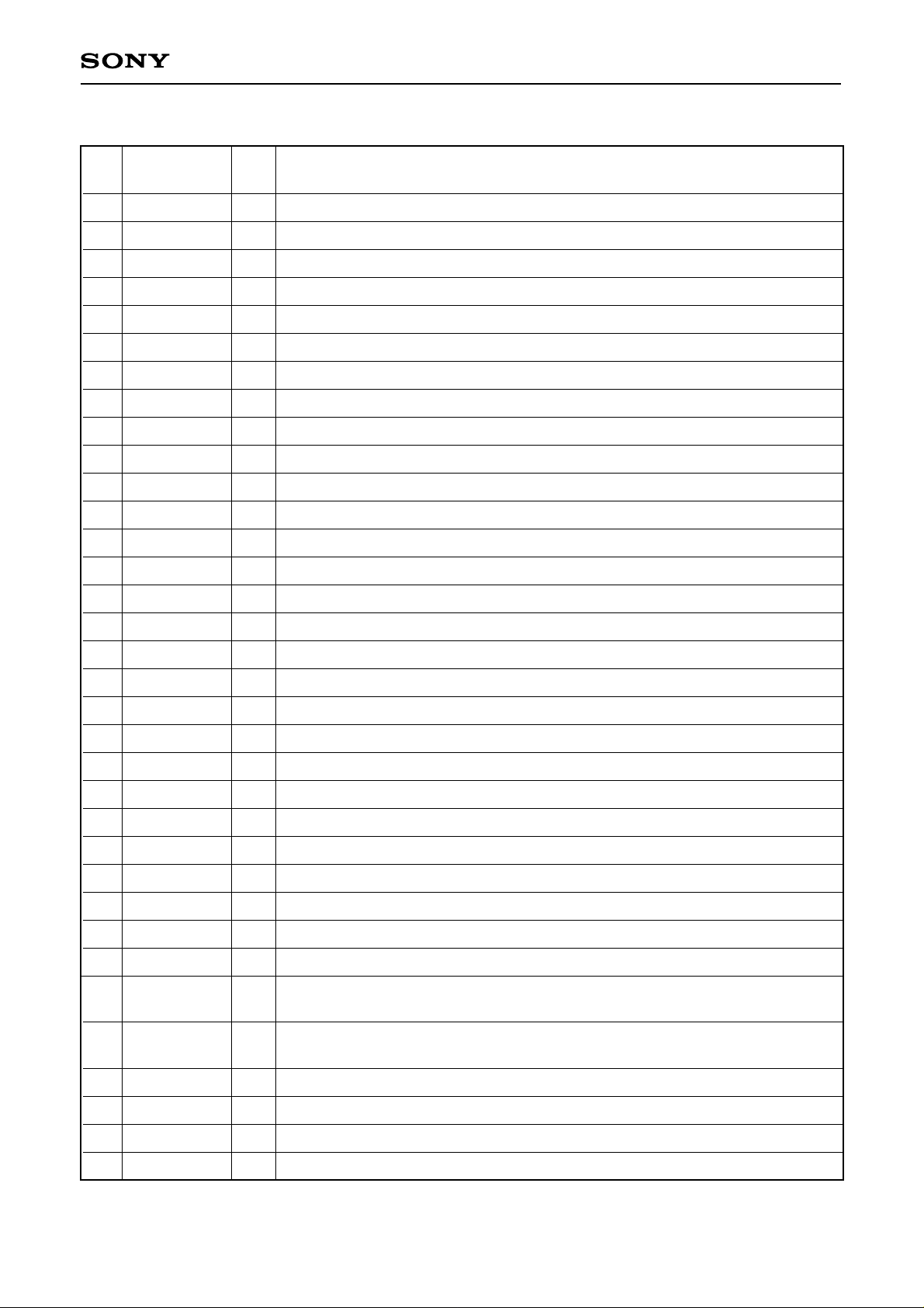
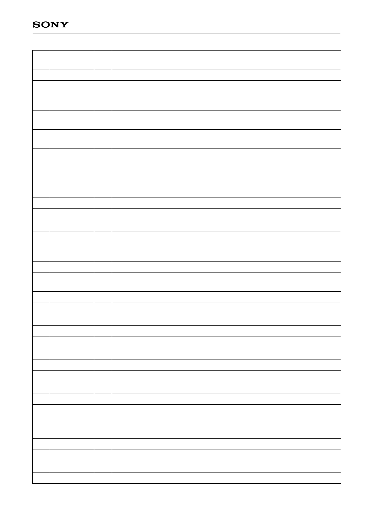
3. Pin Description
CXD1948R
Pin
No.
1
2
3
4
5
6
7
8
9
10
11
12
13
14
15
Symbol I/O
Vss
DATA15
DATA14
DATA13
DATA12
DATA11
DATA10
DATA9
DATA8
VDD
DATA7
DATA6
DATA5
DATA4
DATA3
GND
—
I/O data with host I/F BIT 15
I/O
I/O data with host I/F BIT 14
I/O
I/O data with host I/F BIT 13
I/O
I/O data with host I/F BIT 12
I/O
I/O data with host I/F BIT 11
I/O
I/O data with host I/F BIT 10
I/O
I/O data with host I/F BIT 9
I/O
I/O data with host I/F BIT 8
I/O
Power supply
—
I/O data with host I/F BIT 7
I/O
I/O data with host I/F BIT 6
I/O
I/O data with host I/F BIT 5
I/O
I/O data with host I/F BIT 4
I/O
I/O data with host I/F BIT 3
I/O
Description
16
17
18
19
20
21
22
23
24
25
26
27
28
29
30
DATA2
DATA1
DATA0
Vss
TEST0
TEST1
TEST2
TEST3
TEST4
TEST5
TEST6
TEST7
Vss
XRESET
X8/16
I/O data with host I/F BIT 2
I/O
I/O data with host I/F BIT 1
I/O
I/O data with host I/F BIT 0
I/O
GND
—
Test pin
—
Test pin
—
Test pin
—
Test pin
—
Test pin
—
Test pin
—
Test pin
—
Test pin
—
GND
—
Master reset signal
I
I/O data with host I/F bus select signal
I
∗
∗
∗
∗
∗
∗
∗
∗
0: Active; 1: Non-active
0: 8 bit; 1: 16 bit
ADDRESS6
31
ADDRESS5
32
ADDRESS4
33
ADDRESS3
34
∗
The test pins should be used open.
Host I/F address bus BIT 6
I
Host I/F address bus BIT 5
I
Host I/F address bus BIT 4
I
Host I/F address bus BIT 3
I
– 5 –
Page 6
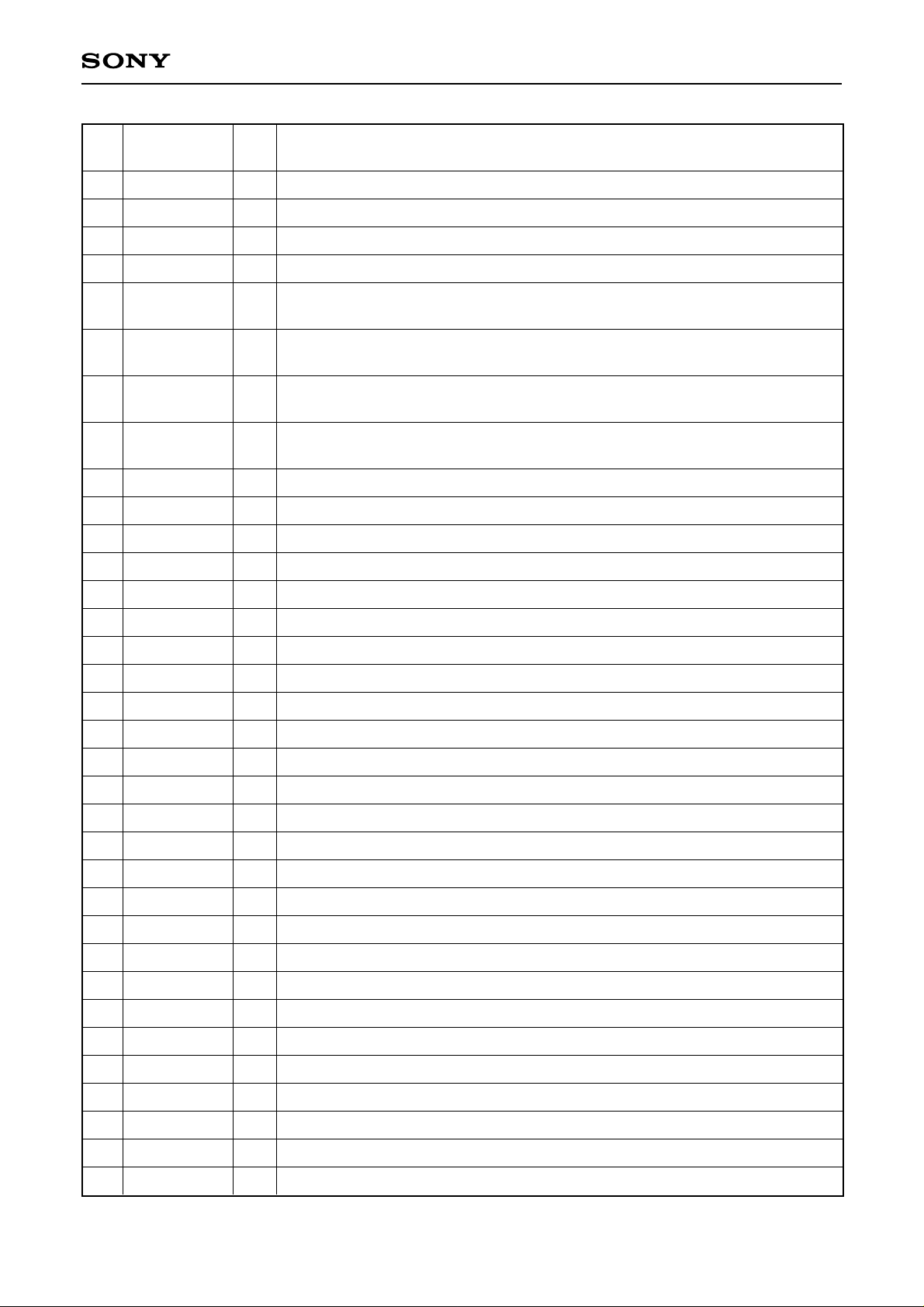
CXD1948R
Pin
No.
35
36
37
38
39
40
41
42
43
44
45
46
47
48
Symbol I/O
ADDRESS2
ADDRESS1
ADDRESS0
VDD
XCS
XWAIT
XW/R
XINT
TEST8
PORT0
PORT1
PORT2
TEST12
TEST13
I
Host I/F address bus BIT 2
I
Host I/F address bus BIT 1
I
Host I/F address bus BIT 0
—
Power supply
Host I/F chip select signal
I
O
I
O
—
I/O
I/O
I/O
—
—
0: Active; 1: Non-active
Host I/F wait signal
0: Active; 1: Non-active
Host I/F write/read signal
0: Write; 1: Read
Host I/F interrupt signal
0: Active; 1: Non-active
Test pin
∗
Parallel I/O port BIT0
Parallel I/O port BIT1
Parallel I/O port BIT2
Test pin
Test pin
∗
∗
Description
49
50
51
52
53
54
55
56
57
58
59
60
61
62
63
64
65
VSS
TEST14
VDD
SYSCLK
VSS
TEST15
TEST16
TEST17
TEST18
D3
D2
D1
D0
VSS
CTL1
CTL0
LREQ
—
GND
—
Test pin
—
Power supply
I
Phy I/F system clock (49.152MHz)
—
GND
—
Test pin
—
Test pin
—
Test pin
—
Test pin
I/O
Phy I/F data bus BIT 3
I/O
Phy I/F data bus BIT 2
I/O
Phy I/F data bus BIT 1
I/O
Phy I/F data bus BIT 0
—
GND
I/O
Phy I/F control bus BIT 1
I/O
Phy I/F control bus BIT 0
O
Phy I/F request signal
∗
∗
∗
∗
∗
66
VDD
67
LPS
68
TEST19
∗
The test pins should be used open.
—
Power supply
O
Phy I/F Link power status signal
—
Test pin
∗
– 6 –
Page 7
CXD1948R
Pin
No.
69
70
71
72
73
74
75
76
77
78
79
80
Symbol I/O
PORT3
PORT4
PACKETGAP
READREQ
ERRFLAG
AIWRITE
AIREAD
VSS
AICK
IFFULL
IFEMPTY
PACKETEN
Description
Parallel I/O port BIT3
I/O
Parallel I/O port BIT4
I/O
Timing signal for adding time stamp to inserted isochronous packet
I
O
I/O
I
I
—
I
O
O
I/O
0: Non-active; 1: Active
Received packet synchronization reference signal
0: Non-active; 1: Active
Packet error signal
0: Non-active; 1: Active
Transport stream I/F data write enable signal
0: Non-active; 1: Active
Transport stream I/F data read enable signal
0: Non-active; 1: Active
GND
Transport stream I/F clock
Isochronous FIFO status output 1: Full
Isochronous FIFO status output 1: Empty
Transport stream I/F packet enable signal
0: Non-active; 1: Active
81
82
83
84
85
86
87
88
89
90
91
92
93
94
95
96
VDD
CK27
IOEC
AIDT15
AIDT14
AIDT13
AIDT12
AIDT11
AIDT10
AIDT9
AIDT8
VSS
AIDT7
AIDT6
AIDT5
AIDT4
Power supply
—
Clock input for 27MHz time stamp (open when not in use)
I
Transport stream I/F data bus control signal
I
I/O
I/O
I/O
I/O
I/O
I/O
I/O
I/O
—
I/O
I/O
I/O
I/O
0: Input; 1: Output
Transport stream I/F data bus BIT 15
Transport stream I/F data bus BIT 14
Transport stream I/F data bus BIT 13
Transport stream I/F data bus BIT 12
Transport stream I/F data bus BIT 11
Transport stream I/F data bus BIT 10
Transport stream I/F data bus BIT 9
Transport stream I/F data bus BIT 8
GND
Transport stream I/F data bus BIT 7
Transport stream I/F data bus BIT 6
Transport stream I/F data bus BIT 5
Transport stream I/F data bus BIT 4
97
AIDT3
98
AIDT2
99
AIDT1
100
AIDT0
∗
The test pins should be used open.
Transport stream I/F data bus BIT 3
I/O
Transport stream I/F data bus BIT 2
I/O
Transport stream I/F data bus BIT 1
I/O
Transport stream I/F data bus BIT 0
I/O
– 7 –
Page 8
CXD1948R
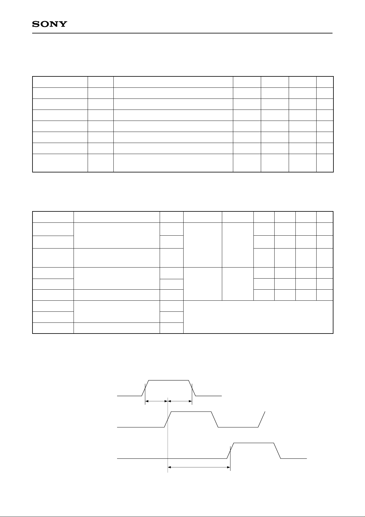
4. Electrical Characteristics
4-1. DC Characteristics (Ta = 25°C, VSS = 0V)
Item Symbol Conditions Min. Typ. Max. Unit
Input voltage
Input voltage
Output voltage
Output voltage
Input leak current
Input leak current
Output leak
current
VIH
VIL
VOH
VOL
II1
II2
IOZ
CMOS input cell
CMOS input cell
IOH = –4.0mA
IOL = 4.0mA
Bidirectional pin (input state)
Normal input pin
Tri-state pin (for high impedance state)
VIN = VSS or VDD
0.7VDD
VDD – 0.4
–40
–10
–40
0.2VDD
0.4
40
10
40
V
V
V
V
µA
µA
µA
4-2. AC Characteristics (VDD = 3.0 to 3.6V)
Item Applicable pin
Input setup
AIDT [15 : 0], ERRFLAG,
PACKETEN, IOEC, AIWRITE,
Input hold
Output delay
AIREAD, PACKETGAP
AIDT [15 : 0], ERRFLAG,
READREQ
Symbol
Tsu1
Th1
Td1
Normal clock
AICK
AIREAD
AIWRITE
∗1
Conditions Min. Typ. Max. Unit
CL = 10pF
10
5
40
ns
0
ns
ns
Input setup
Tsu2
D [3 : 0], CTL [1 : 0]
Input hold
Output delay
Input setup
Input hold
Output delay
∗1
During asynchronous I/F, the reference clock is AIWRITE (transmit)/AIREAD (receive).
D [3 : 0], CTL [1 : 0], LREQ
ADDRESS [6 : 0],
DATA [15 : 0], XCS, XWR
DATA [15 : 0], XWAIT, XINT
Th2
Td2
Tsu3
Th3
Td3
SYSCLK
CL = 10pF
Refer to P.31 ATF/CFR/IPF write timing
ATF/CFR read timing
4-3. Timing Definitions
Input
Tsu Th
reference clock
5
2
2
15
ns
ns
ns
Output
Td
– 8 –
Page 9
CXD1948R
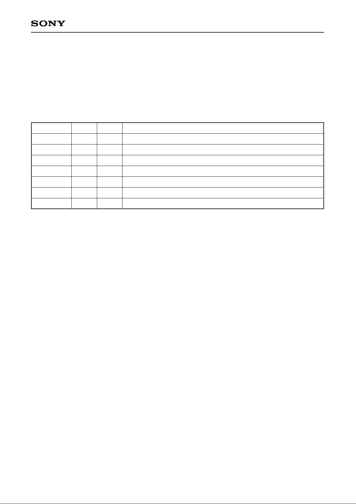
5. Isochronous Communication
The CXD1948R has a function which transmits and receives DVB and DSS transport stream data as
isochronous packets.
The communication of transport stream data with the DVB and DSS systems is performed using a dedicated
I/O data bus and several control signal pins. (See below.)
Further, it supports a wide variety of application I/F, including 8-bit data and 16-bit data, synchronous and
asynchronous.
Name
AIDT
PACKETEN
ERRFLAG
AIWRITE
AIREAD
READREQ
AICK
Width
16
1
1
1
1
1
1
in/out
in/out
in/out
in/out
in
in
out
in
Description
Transport stream data bus
Indicates a valid packet (valid: 1; invalid: 0)
Indicates that the packet is an error (error: 1; no error: 0)
Data write strobe signal
Data read strobe signal
Packet read request signal
Clock for interface (during sync)
5-1. Built-in FIFO
The CXD1948R has a built-in dedicated FIFO for isochronous communication.
The FIFO capacity is 3840 bytes, and it can accumulate 20 packets worth of DVB transport stream.
In order to actually use the built-in FIFO, the bank structure must be set. This is performed by the CFR
PacketBanks register.
– 9 –
Page 10
CXD1948R
5-2. Transport Stream Data I/F
5-2-1. Data Bus
The data interface is 8 bit/16 bit, and switching is done by accessing the CFR AIDT16 register. (The default
value is 8 bit.)
5-2-2. Transport Packet Size
Data communication is done in transport stream packet units.
The data size for one packet can be set optionally by accessing the S_PacketSize register on the CFR.
S_PacketSize expresses the byte size of 1 source packet for isochronous communication.
For DVB specifications, this is 192 (data 188 bytes, source packet header 4 bytes).
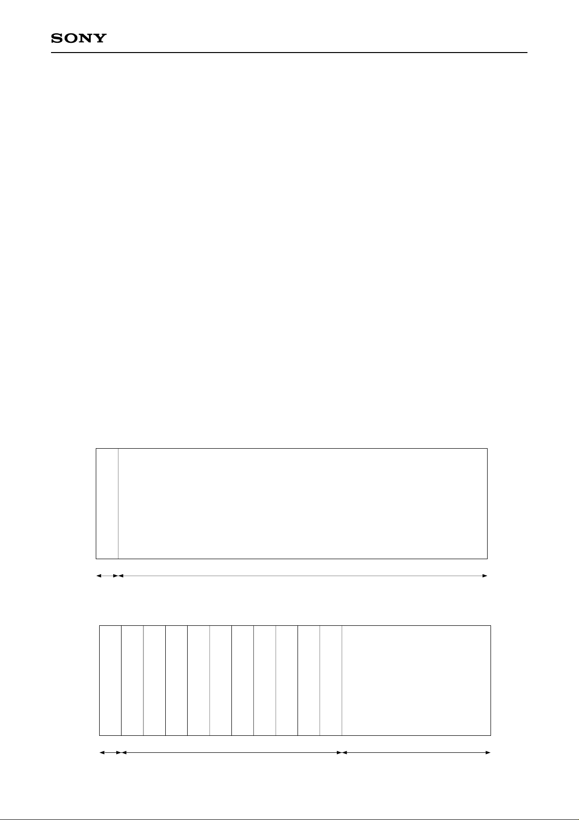
5-2-3. Isochronous Additional Data
Optional data can be added to the transport stream packet when isochronous communication is performed.
Setting of the additional data is done by setting the CFR AddSize and AddData1 to AddData10 registers.
AddSize is a 4-bit register, and expresses the number of additional bytes for isochronous transmit/receive.
AddData1 to AddData10 are each 8-bit registers, and express the additional data for isochronous transmit/receive.
The default setting is no additional data.
The additional data is inserted between the source packet header and the transport stream data.
The smallest group of data that can be handed under IEEE1394 is 32 bits, so the setting must be such that the
total of the transport stream data and additional data is a 32-bit unit.
An example is shown below.
Example of Isochronous Communication Setting
When S_PacketSize = 192 and AddSize = 0 (example of setting for DVB)
SPH
Transport stream data
188 bytes4 bytes
When S_PacketSize = 144 and TxAddSize = 10 (example of setting for DSS)
SPH
Transport stream data
Additional data 3
Additional data 2
Additional data 1
Additional data 5
Additional data 4
Additional data 6
10 bytes4 bytes
Additional data 9
Additional data 8
Additional data 7
– 10 –
Additional data 10
130 bytes
Page 11
CXD1948R
5-2-4. Transmit Interface
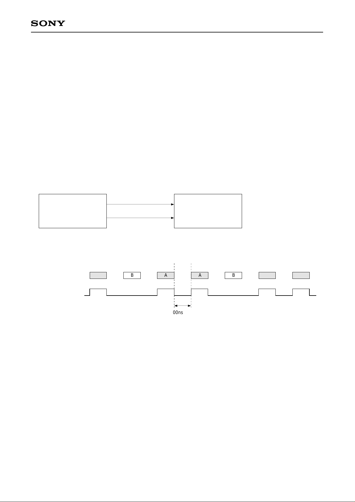
The CXD1948R is designed for use not only in transmitting an entire input transport stream, but also in
transmitting one program only in the stream. The packet for transmission is selected through PACKETEN input
as in the diagram below.
Moreover, constraints are imposed in the packet intervals of streams that can be input to the CXD1948R.
Each time the CXD1948R receives one packet of transport stream data, it adds time stamp data and data from
the host I/F, and there must be an interval of 500ns or more for this processing. The timing is illustrated below.
Also, the PACKETEN input signal must input “HIGH” while the first data of the transport stream packet is being
sent. The maximum period for PACKETENABLE signal high is the period that the transport stream packet data
is valid.
The timing charts for synchronous/asynchronous interface are shown below.
Transmit Interface Limits
AIDT
MPEG2 transporter CXD1948R
Transmission of Program A
AIDT
PACKETEN
A
PACKETEN
B A A
500ns (min)
B A A
– 11 –
Page 12
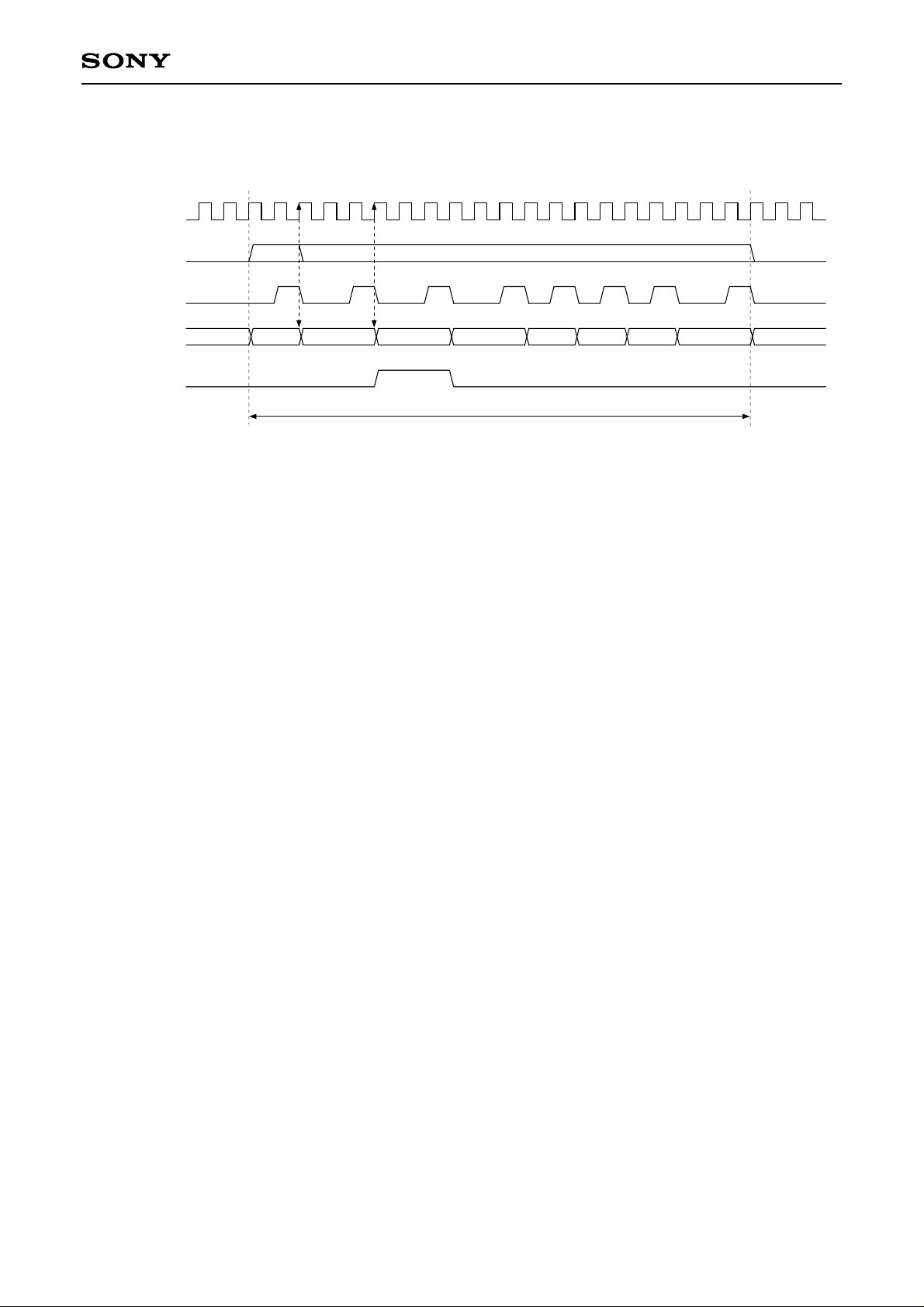
Transmit Interface (for sync mode/8 bit/Nbyte)
AICK
CXD1948R
PACKETEN
AIWRITE
AIDT
ERRFLAG
Don’t Care
first data
taken in
second data
taken in
Valid interval for transport stream packet
Don’t Care
Don’t CareN – 1N – 2N – 3········3210
Sync interface mode is obtained by setting the CFR AsyncAI register to 0. (The default is 0.)
The CXD1948R identifies the first data of the transport stream packet by detecting that the PACKETEN signal
has gone from low to high.
There is no particular need to input the PACKETEN signal after the first data. The size of the data taken in as
valid data is equal to the value set in the CFR S_PacketSize register, decreased by 4 and by the value set in
the AddSize register. The timing for taking in of the data internally is done by AICK rise when AIWRITE is
high.
The AIWRITE signal is used as the enable signal, so the interval that the AIWRITE signal is high relative to
one data must be one AICK clock interval. The interval that the AIWRITE signal is low relative to one data is
not specified.
The limits on AICK input frequency are given below.
For 8-bit data input: 40MHz (Max.), 2MHz (Min.)
For 16-bit data input: 20MHz (Max.), 2MHz (Min.)
The ERRFLAG input during transmit can be made valid by setting the CFR ErrBitEnable register to 1. (The
default is 0.)
The CXD1948R identifies the subject packet as an error if the ERRFLAG input is high for even one data
during transport stream packet valid interval.
The switching timing for ERRFLAG input can be changed in the same way as data switching timing, with
AIWRITE signal rise.
– 12 –
Page 13
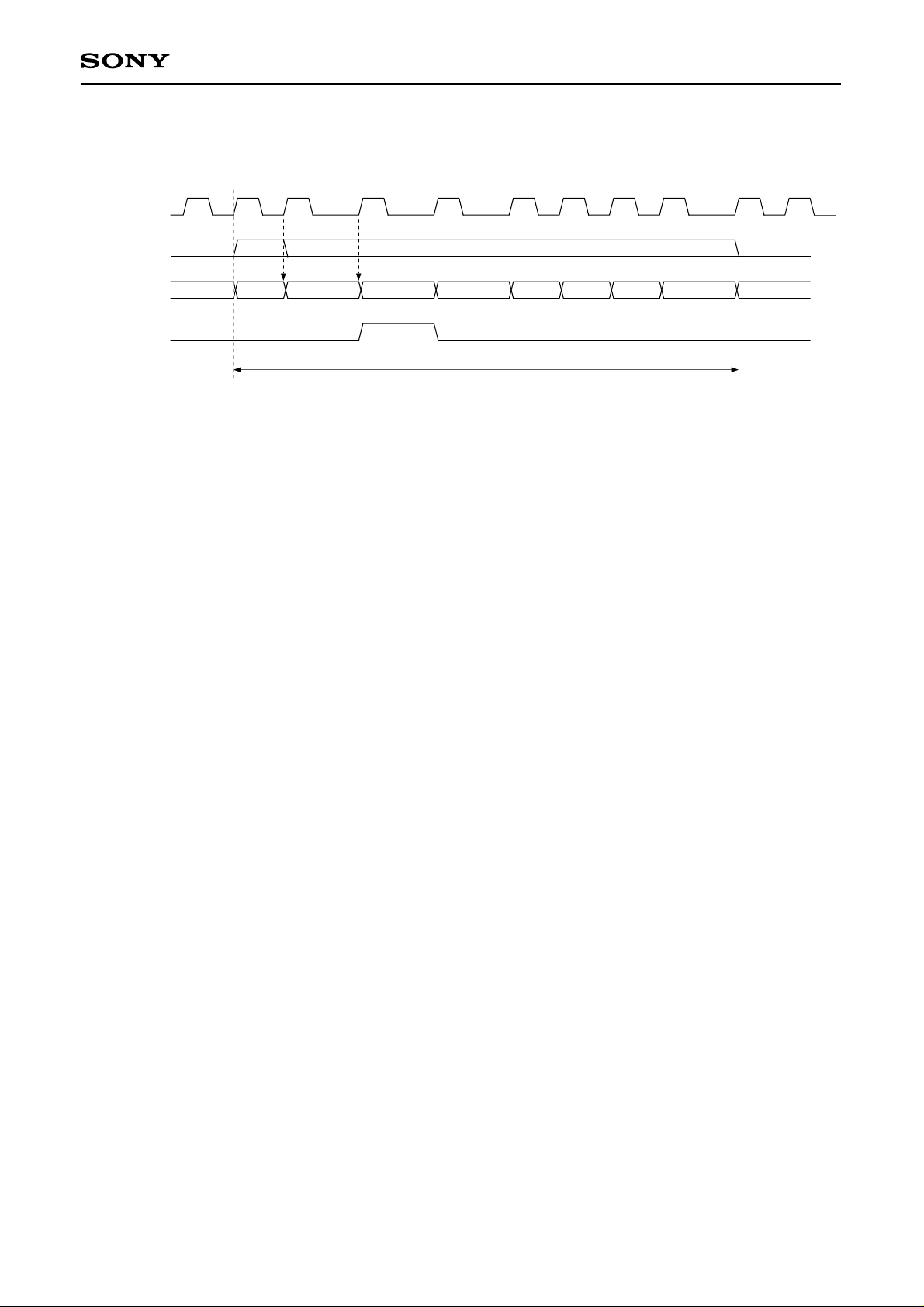
Transmit Interface (for asynchronous mode/8 bit/Nbyte)
AIWRITE
CXD1948R
PACKETEN
AIDT
ERRFLAG
Don’t Care
first data
taken in
second data
taken in
Valid interval for transport stream packet
Don’t Care
Don’t CareN – 1N – 2N – 3········3210
Asynchronous interface mode is obtained by setting the CFR AsyncAI register to 1. (The default is 0.)
The CXD1948R identifies the first data of the transport stream packet by detecting that the PACKET_EN
signal has gone from low to high.
There is no particular need to input the PACKET_EN signal after the first data.
The size of the data taken in as valid data is equal to the value set in the CFR S_PacketSize register,
decreased by 4 and by the value set in the AddSize register. The timing for taking in of the data internally is
done by AIWRITE rise.
The AIWRITE input is used as the clock, so there must be one AIWRITE input rising edge relative to one data.
AIWRITE input duty is not specified, but the AIWRITE input must continue to be input evenly as the clock even
outside of the transport stream packet valid interval.
The limits on AIWRITE input frequency are given below.
For 8-bit data input: 20MHz (Max.), 1MHz (Min.)
For 16-bit data input: 10MHz (Max.), 1MHz (Min.)
The ERRFLAG input during transmit can be made valid by setting the CFR ErrBitEnable register to 1. (The
default is 0.)
The CXD1948R identifies the subject packet as an error if the ERRFLAG input is high for even one data
during transport stream packet valid interval.
The switching timing for ERRFLAG input can be changed in the same way as data switching timing, with
AIWRITE signal rise.
– 13 –
Page 14
CXD1948R
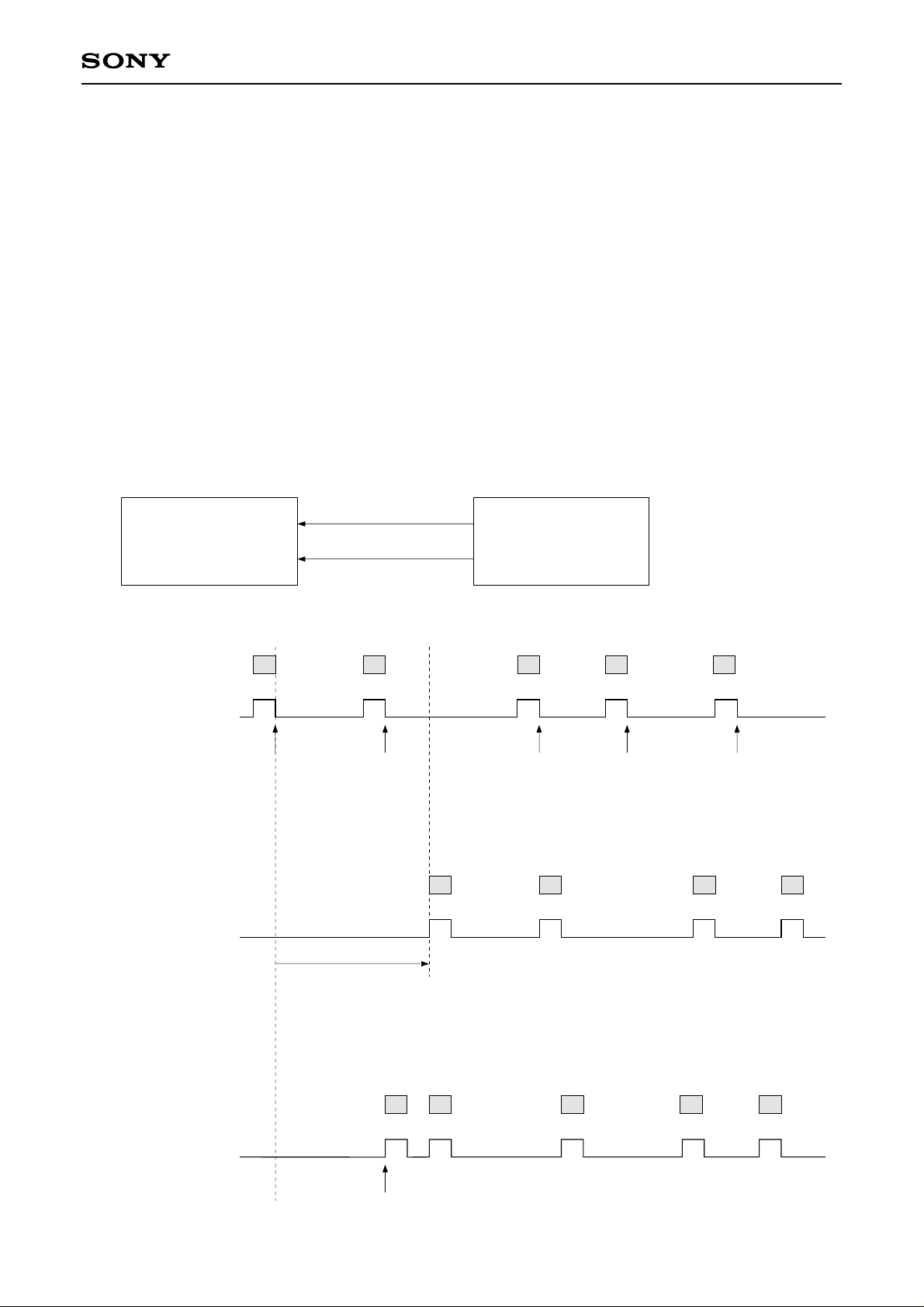
5-2-5. Receive Interface
The CXD1948R supports two modes; one in which data is output based on the time stamp value added to the
transport stream packet during transmission, and one in which the data is output consecutively as soon as it is
ready, without using the time stamp.
When output is based on the time stamp value, the actual output timing is done using a value which is the time
stamp value with a fixed delay added. This is done in order to keep the packet intervals even on the transmit
and receive sides.
When the time stamp value is not used for output, data output begins when the packet has completely arrived
at the receive side. In this case, the time required for the packet to be sent and arrive completely at the receive
side varies for each isochronous cycle, and packet interval on the transmit side can not be guaranteed.
The timing is shown below.
The mode in which the time stamp is not used can be set by setting the CFR TmsDis register to 1. (The default
is 0.)
Receive Interface
D-VHS system CXD1948R
Transmit I/F
AIDT
PACKETEN
Time stamp
added timing
Receive I/F
Time stamp function used
AIDT
PACKETEN
AIDT
PACKETEN
12
12 34
Fixed delay
3 4
5
Time stamp function not used
AIDT
PACKETEN
12 3 4 5
Time when packet 1
output is ready
– 14 –
Page 15
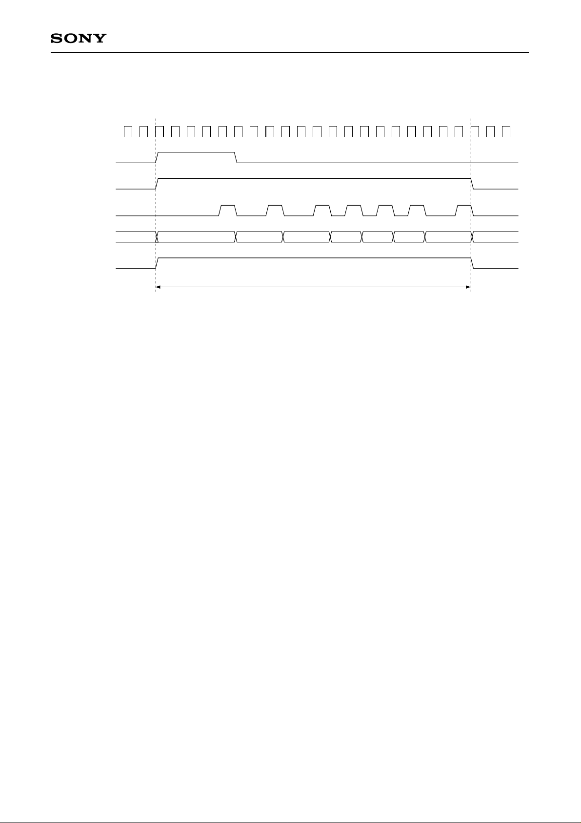
Receive Interface (for sync mode/8 bit/Nbyte)
AICK
READREQ
PACKETEN
AIREAD
CXD1948R
AIDT
ERRFLAG
Don’t Care Don’t CareN – 1N – 2N – 3········210
Valid interval for transport stream packet
Sync interface mode is obtained by setting the CFR AsyncAI register to 0. (The default is 0.)
The CXD1948R outputs the first data of the transport stream packet by changing the READREQ output signal
and PACKETEN output signal from low to high when the packet has been completely received and is ready for
output.
The READREQ output signal goes low when the first data is output.
The same as for transmit, the result of subtracting 4 and the value set in the AddSize register from the value
set in the CFR S_PacketSize register is used as the size of the valid data output in one packet. The timing is
done by the AICK rise when AIREAD is high.
The AIREAD signal is used as the enable signal, so the interval that the AIREAD signal is high relative to one
data must be one AICK clock interval. The interval that the AIREAD signal is low relative to one data is not
specified.
The limits on AICK input frequency are given below.
For 8-bit data input: 40MHz (Max.), 2MHz (Min.)
For 16-bit data input: 20MHz (Max.), 2MHz (Min.)
The ERRFLAG input during receive can be made valid by setting the CFR ErrBitEnable register to 1. (The
default is 0.)
The CXD1948R outputs the ERRFLAG at high during the valid interval if the output transport stream packet is
an error.
The switching timing for ERR_FLAG input can be changed in the same way as data switching timing, with
AIREAD signal rise.
– 15 –
Page 16
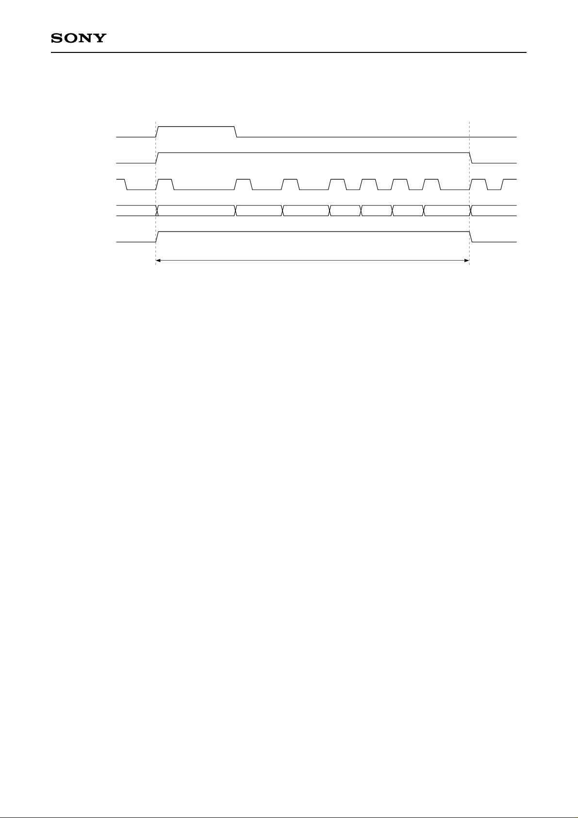
Receive Interface (for asynchronous mode/8 bit/Nbyte)
READREQ
PACKETEN
AIREAD
CXD1948R
AIDT
ERRFLAG
Don’t Care Don’t CareN – 1N – 2N – 3········210
Valid interval for transport stream packet
Sync interface mode is obtained by setting the CFR AsyncAI register to 0. (The default is 0.)
The CXD1948R outputs the first data by changing the READREQ output signal and PACKETEN output signal
from low to high when the packet has been completely received and is ready for output.
The READREQ output signal goes low when the first data is output.
The same as for transmit, the result of subtracting 4 and the value set in the AddSize register from the value
set in the CFR S_PacketSize register is used as the size of the valid data output in one packet. The timing is
done by the AIREAD signal rise.
The AIREAD signal is used as the clock, so there must be one AIREAD input rising edge relative to one data.
AIREAD input duty is not specified, but the AIREAD input must continue to be input evenly as the clock even
outside of the transport stream packet valid interval.
The interval that the AIREAD signal is low relative to one data is not specified.
The limits on AICK input frequency are given below.
For 8-bit data input: 20MHz (Max.), 1MHz (Min.)
For 16-bit data input: 10MHz (Max.), 1MHz (Min.)
The ERRFLAG input during receive can be made valid by setting the CFR ErrBitEnable register to 1. (The
default is 0.)
The CXD1948R outputs the ERRFLAG at high during the valid interval if the output transport stream packet is
an error.
The switching timing for ERR_FLAG input can be changed in the same way as data switching timing, with
AIREAD signal rise.
– 16 –
Page 17

CXD1948R
5-2-6. Using the ERRFLAG Pin
The CXD1948R can function as a transport stream data interface using error information.
Concretely, this is done using the ERRFLAG pin.
Like other transport stream data interfaces, the ERRFLAG pin is a bidirectional pin. I/O switching is performed
by the CFR IGFMode register.
Also, ERRFLAG control is performed by the CFR ErrBitEn and ErrOutEn registers.
The settings when using ERRFLAG during transmit and receive are given below.
Transmit settings
The ERRFLAG input can be made valid by setting the CFR ErrBitEn register to “1”. (The default is “0”.)
In order to add the error information provided by ERRFLAG to an isochronous packet and transmit this
information, the added data must be 4 bytes or more.
Concretely, the CFR AddSize register value must be 4 or larger.
Both of the conditions below must be met to send error information using the ERRFLAG pin during transmit.
(1) The ErrBitEn register is 1.
(2) The AddSize register is 4 or higher.
Receive settings
The ERRFLAG output can be made valid by setting the CFR ErrOutEn register to “1”. (The default is “0”.)
The CXD1948R handles received packet errors in two ways as follows.
(1) Packets with error information added to the transport stream data
In this case, the error information must be added to the received isochronous packet.
In addition, the CFR ErrBitEn register must be set to 1.
(2) Error packets occurring during isochronous communication
These errors refer to packets received with non-consecutive DBC values due to CRC errors or Late
processing during transmit.
In this case, only the CFR ErrOutEn register is set.
Setting this register to “1” inserts an error packet between packets with non-consecutive DBC values.
As a result, one packet of ERRFLAG = 1 data is read by the transport stream data interface.
If the ErrOutEn register is set to 0, this processing is not performed.
Non-consecutive DBC values also result when the receive FIFO overflows, and the processing is the same
in these cases as well.
– 17 –
Page 18
CXD1948R
5-3. Transport Stream Packet Split and Combine Functions
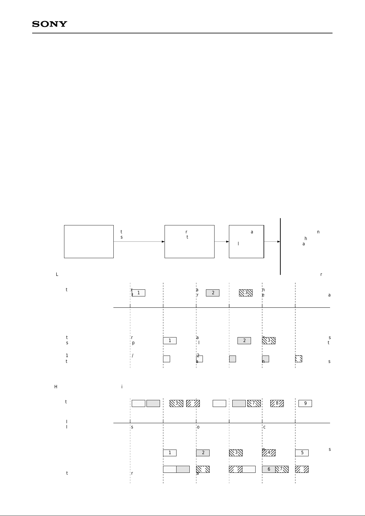
The CXD1948R supports split and combine functions in order to use the bus bandwidth effectively.
Concretely, the input transport stream packet can be split or combined according to the input rate and
transmitted as an isochronous packet.
The minimum size which can be split on the CXD1948R is one data block.
For DVB specifications, one data block consists of 24 bytes, which means that 1 packet can be divided into
eighths for transmission.
The maximum size which can be combined is 15 packets. However, if the number of packets which can be
transmitted in that cycle is smaller than the number that can be combined, all the packets present are
combined in the transmission FIFO buffer and transmitted.
The number of data blocks to be transmitted in one isochronous cycle is set before hand according to the
stream peak rate.
This is done by setting values in the CFR NOSP and NODB registers.
The number of transmit source packets in one isochronous cycle is expressed by NOSP, and the number of
transmit data blocks in one isochronous cycle is expressed by NODB.
The default values are NOSP = 0001 and NODB = 000, for transmission of one source packet in one
isochronous cycle. Always be sure to set either NOSP or NODB to 0.
If the isochronous transmission parameters are not set such that the transmission rate is greater than the input
stream peak rate, the FIFO buffer may fail.
Example of Isochronous Transmit using Packet Split and Combine Functions
transport
MPEG2 transporter
Low rate
transport
stream data
IEEE1394
Isochronous
transmit without
splitting
1/2 packet
transmit
stream data
1
CXD1948R
2
1 2
12
12
Physical
layer LSI
3
IEEE1394 bus
3
3
High rate
transport
stream data
IEEE1394
Isochronous
transmit without
combining
2 packet
transmit
12
3
4
12
12
56
3
7
3
4
56
8
4
7
9
5
8
– 18 –
Page 19
CXD1948R
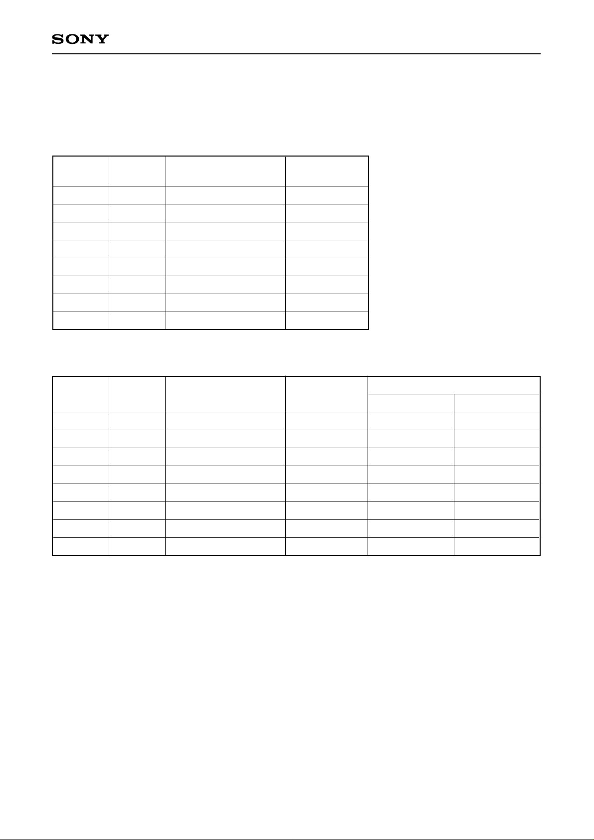
5-4. Transport Stream Data Bandwidth
The bandwidths on which transport stream data can be transmitted on the CXD1948R are illustrated below.
DVB
DSS
NOSP
value
0000
0000
0000
0001
0010
0011
0100
0101
NOSP
value
0000
0000
NODB
value
001
010
100
000
000
000
000
000
NODB
value
001
010
No. of transmit data
1 data block
2 data blocks
4 data blocks
1 source packet
2 source packets
3 source packets
4 source packets
5 source packets
No. of transmit data
1 data block
2 data blocks
Transmittable
data rate
1.5Mbps
3.0Mbps
6.0Mbps
12.0Mbps
24.0Mbps
36.0Mbps
48.1Mbps
60.1Mbps
Transmittable
data rate
2.2Mbps
4.4Mbps
Transmittable data rate
Addsize = Ah Addsize = 0h
2.0Mbps
4.1Mbps
2.2Mbps
4.4Mbps
0001
0010
0011
0100
0101
0110
000
000
000
000
000
000
1 source packet
2 source packets
3 source packets
4 source packets
5 source packets
6 source packets
8.9Mbps
12.0Mbps
26.8Mbps
35.8Mbps
44.8Mbps
53.7Mbps
8.3Mbps
16.6Mbps
24.9Mbps
33.2Mbps
41.6Mbps
49.9Mbps
8.9Mbps
17.9Mbps
26.8Mbps
35.8Mbps
44.8Mbps
53.7Mbps
– 19 –
Page 20
CXD1948R
A
A
5-5. Isochronous Packet Structure
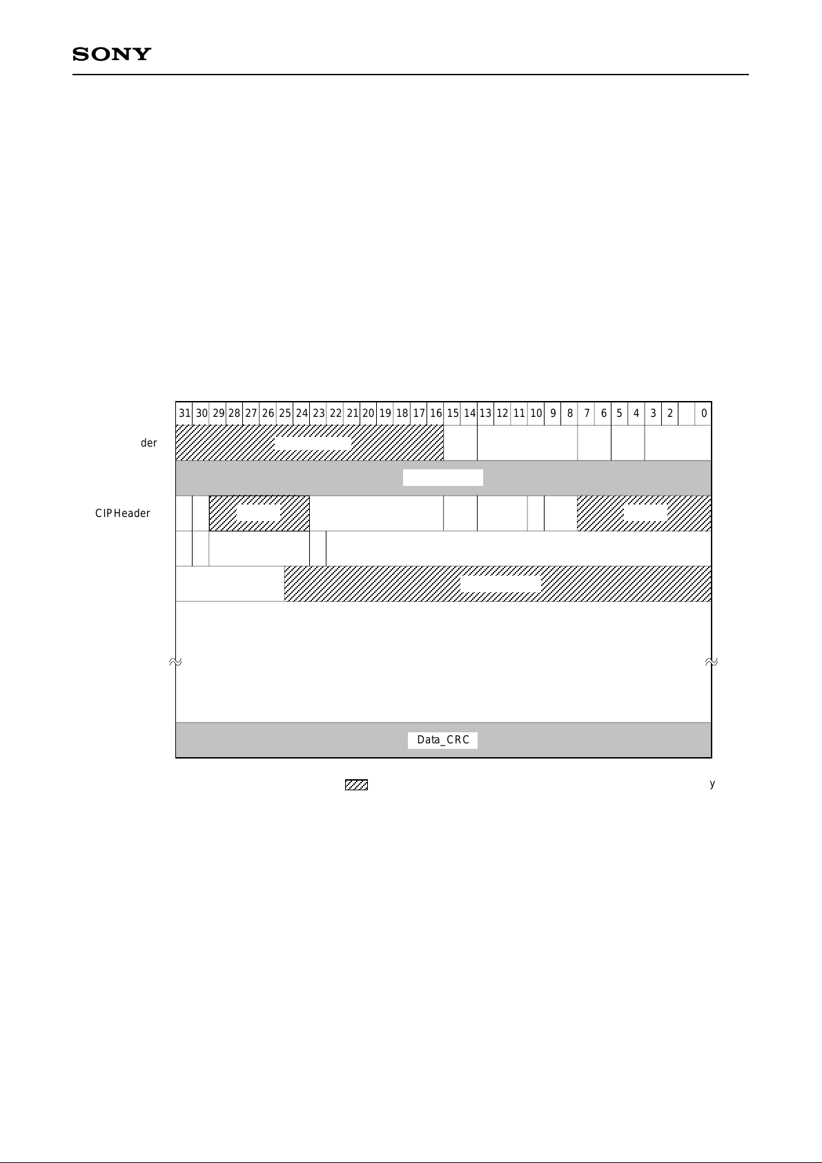
The basic isochronous packet structure supported by the CXD1948R is illustrated below.
On the CXD1948R, CIPHeaders 1 and 2 are automatically attached/detected in conformity to AV protocol.
Also, a source packet header is automatically added/detected on the transport stream packet based on the
MPEG Data Transmission for IEEE1394 Digital Interface specifications proposed in DVB-SMI.
When one source packet is transmitted in one isochronous cycle, 1st quadlet is 1394Header, 2nd quadlet is
Header_CRC (added at Link Core), 3rd quadlet is CIPHeader1, 4th quadlet is CIPHeader2, 5th quadlet is source
packet header and 6th quadlet and after is the data area. The final quadlet is Data_CRC (added at Link Core).
When a dummy packet is transmitted, there are only 1394Header, Header_CRC, CIPHeader1, CIPHeader2
and Data_CRC.
Basic Structure
031302928272625242322212019181716151413121110987654321
1394Header
CIPHeader1
CIPHeader2
SPHeader
reserved
reserved
speed sytag
DBC
AAA
data length
Header CRC
0 0 QPC
10
Note: The diagonally shaded areas ( ) for 1394Header and CIPHeader1 and 2 are attached automatically by
the CXD1948R. Other areas are set from the external microcomputer via the host I/F.
In transmission from the CXD1948R to an IEEE 1394PHYIC, the four bits marked "reserved" and "speed"
of the 1394Header are automatically replaced by "tcode".
SID
AA
FMT
TF
DBS FN
Data
Data_CRC
channel
SPH
FDF
TimeStampReserved
– 20 –
Page 21
1394Header Fields
CXD1948R
Field Name
data_length
Indicates the byte length of data from CIPHeader1.
Description
Type of format for data transferred as isochronous packet.
00: no Header
tag
01: format defined by AV protocol
10: Reserved
11: Reserved
channel
Channel number used by the transmitted packet.
Defines transfer speed.
00: 100Mbit/s
speed
01: 200Mbit/s
10: 400Mbit/s
11: Undefined
The CXD1948R supports “00” and “01”.
sy
This field is defined by the application.
Note: The Link Core must be informed of the communication speed in the case of isochronous communication,
so [5 : 4] of [7 : 4], where a tCode is inserted, is used as the speed code. This is replaced with tCode
(1010) at the Link Core.
CIPHeader1 Fields
Field Name
SID
DBS
FN
QPC
SPH
DBC
CIPHeader2 Fields
Field Name
FMT
Description
The CXD1948R Node ID. (0 to 3Fh)
The number of quadlets transferred in one isochronous packet.
For DVB specifications, this is “00000110b” and for DSS specifications, “00001001b”.
Indicates how many data blocks a source packet is divided into.
The number of quadlets added to an incomplete packet when the source packet
is split. Fixed at “0h” on the CXD1948R.
Expresses whether a source packet header is used or not. Fixed at “1” on the
CXD1948R.
Increased by one for each data block. This is a free run continuity counter.
When multiple data blocks are to be sent as a single isochronous packet,
indicates the value for the first data block.
Description
Data format ID.
This is “100000b” for DVB and “100001b” for DSS specifications.
TF
FDF
Indicates whether data is time-shifted. 1 if time-shifted; 0 if not time-shifted.
Used in application defined by FMT.
The value set via the host I/F is input as is on the CXD1948R.
– 21 –
Page 22
SPHeader fields
CXD1948R
Field Name
Reserved
TimeStamp
The value set via the host I/F is input as is on the CXD1948R.
This is the value of the time that the transport stream packet arrived at the
CXD1948R plus the fixed delay value.
Description
5-5-1. DVB Format
The DVB format supported by the CXD1948R is described below.
The CFR S_PacketSize and AddSize registers are set as shown below when using the CXD1948R in DVB
format.
S_PacketSize: 0C0h
AddSize: 0h
Next, the NOSP and NODB registers are set. These determine how many data are to be transmitted/received
in one isochronous cycle.
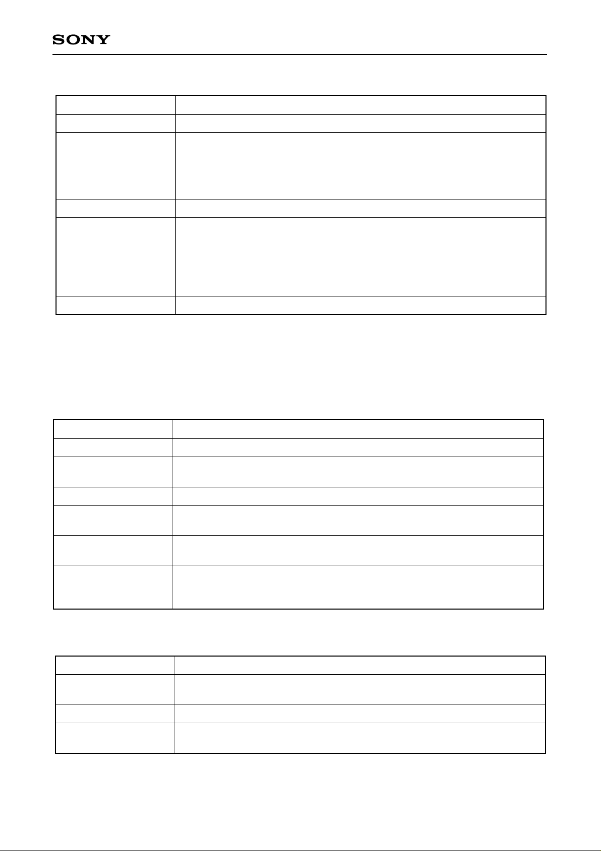
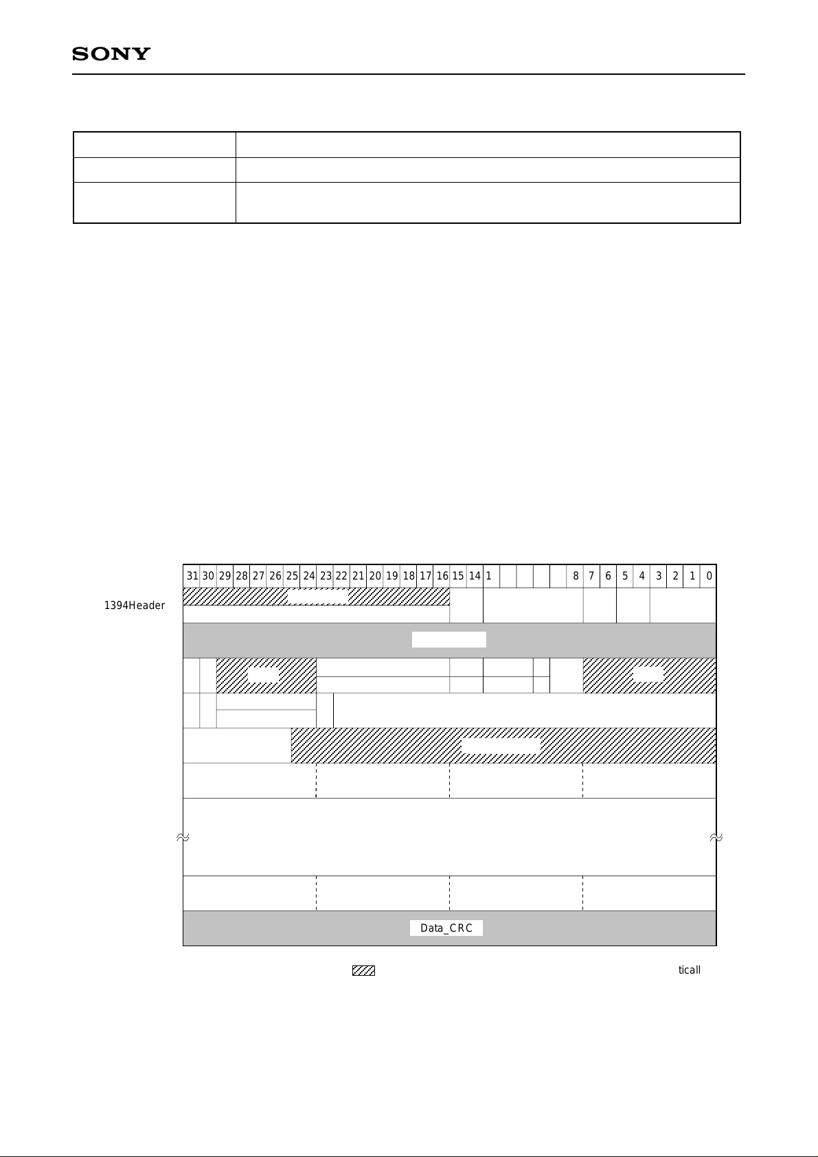
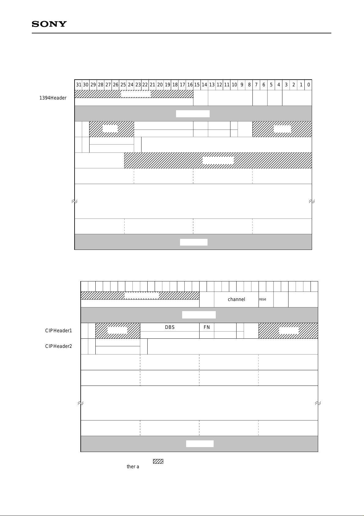
The structures of isochronous packets for transmit/receive of data consisting of 1 source packet, 4 data blocks
or 2 source packets in one isochronous cycle are illustrated below.
DVB/Isochronous Packet Structure (1 source packet)
1394Header
CIPHeader1
CIPHeader2
SPHeader
031302928272625242322212019181716151413121110987654321
data_length
00C8h
Header_CRC
00
10
Note: The diagonally shaded areas ( ) for 1394Header and CIPHeader1 and 2 are attached automatically by
the CXD1948R. Other areas are set from the external microcomputer via the host I/F.
In transmission from the CXD1948R to an IEEE 1394PHYIC, the four bits marked "reserved" and "speed"
of the 1394Header are automatically replaced by "tcode".
SID
FMT
20h
Reserved
data0 data1 data2 data3
data184 data185 data186 data187
TF
DBS FN
06h 11 000
Data (188 bytes)
Data_CRC
channel
QPC
FDF
TimeStamp
SPH
1
reserved
reserved
speed sytag
DBC
– 22 –
Page 23
DVB/Isochronous Packet Structure (4 data blocks)
(First half data)
SID
FMT
20h
data_length
0068h
DBS FN
06h 11 000
TF
1394Header
CIPHeader1
CIPHeader2
00
10
Header_CRC
QPC
FDF
channel
SPH
1
reserved
reserved
CXD1948R
031302928272625242322212019181716151413121110987654321
speed sytag
DBC
SPHeader
(Second half data)
1394Header
CIPHeader1
CIPHeader2
TimeStampReserved
data0 data1 data2 data3
Data (92 bytes)
data88 data89 data90 data91
Data_CRC
data_length
0068h
channel
Header_CRC
00
10
SID
FMT
20h
DBS FN
06h 11 000
TF
QPC
FDF
SPH
reserved
1
reserved
031302928272625242322212019181716151413121110987654321
speed sytag
DBC
data92 data93 data94 data95
data96 data97 data98 data99
Data (96 bytes)
data184 data185 data186 data187
Data_CRC
Note: The diagonally shaded areas ( ) for 1394Header and CIPHeader1 and 2 are attached automatically by
the CXD1948R. Other areas are set from the external microcomputer via the host I/F.
In transmission from the CXD1948R to an IEEE 1394PHYIC, the four bits marked "reserved" and "speed"
of the 1394Header are automatically replaced by "tcode".
– 23 –
Page 24
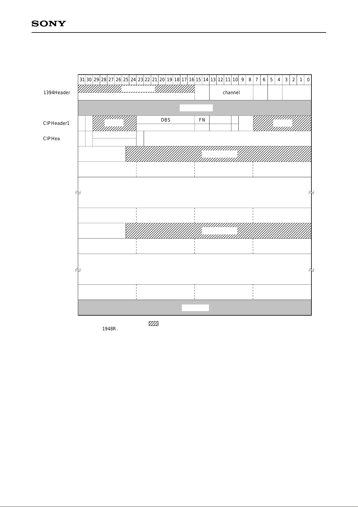
DVB/Isochronous Packet Structure (2 source packets)
SID
FMT
20h
data_length
0184h
DBS FN
06h 11 000
TF
1394Header
CIPHeader1
CIPHeader2
00
10
Header_CRC
QPC
FDF
channel
SPH
1
reserved
reserved
CXD1948R
031302928272625242322212019181716151413121110987654321
speed sytag
DBC
SPHeader
SPHeader
TimeStampReserved
data0 data1 data2 data3
Data (188 bytes)
data184 data185 data186 data187
TimeSrampReserved
data0 data1 data2 data3
Data (188 bytes)
data184 data185 data186 data187
Data_CRC
Note: The diagonally shaded areas ( ) for 1394Header and CIPHeader1 and 2 are attached automatically by
the CXD1948R. Other areas are set from the external microcomputer via the host I/F.
In transmission from the CXD1948R to an IEEE 1394PHYIC, the four bits marked "reserved" and "speed"
of the 1394Header are automatically replaced by "tcode".
– 24 –
Page 25
CXD1948R
5-5-2. DSS Format
The DSS format supported by the CXD1948R is described below.
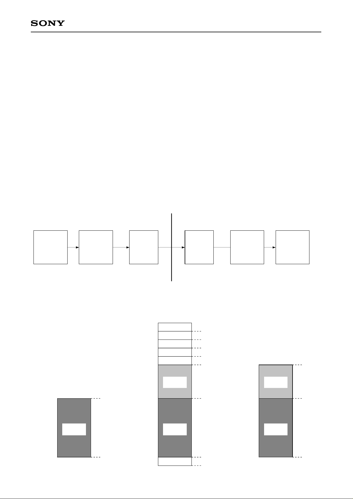
The interface with the system and the CFR setting differ according to whether the CXD1948R is used as DSSSTB or DSS-DVHS system digital I/F, as follows:
A) DSS-STB system digital I/F: S_PacketSize: 090h; AddSize: 0h
B) DSS-DVHS system digital I/F: S_PacketSize: 090h; AddSize: Ah
The isochronous data format on the IEEE1394 bus does not change for A and B. Only the amount of data
interfaced with the system changes.
The DSS-STB system interfaces with 130 bytes as one packet of transport stream.
The CXD1948R adds a 4-byte source packet header and 10 bytes of data set on the CFR via the host I/F to
the received 130 bytes, then transmits them as an isochronous packet.
For the DSS-DVHS system, only the source packet header is removed from the received isochronous packet,
and 140 bytes of data are output as transport stream data.
The above is for the case of transmission; in reception, 140 bytes of data is input from the DSS-DVHS system,
and 130 bytes of data is output to the DSS-STB system.
The same as for the DVB format, the amount of data transmitted in one isochronous cycle is set by the NOSP
and NODB registers.
Example of Interface with DSS System
DSS-STB
system
CXD1948R
S_PacketSize : 090H
AddSize : Ah
IEEE1394
Physical
layer LSI
IEEE1394
Serial Bus
IEEE1394
Physical
layer LSI
Isochronous packet
on IEEE1394 bus
1394header
headerCRC
CIPheader1
CIPheader2
SPheader
Additional
Data
4 bytes
4 bytes
4 bytes
4 bytes
4 bytes
10 bytes
CXD1948R
S_PacketSize : 090H
AddSize : 0h
Interface with DSS-DVHS systemInterface with DSS-STB system
Additional
Data
DSS-DVHS
system
10 bytes
Payload
Data
130 bytes
Payload
Data
Data_CRC 4 bytes
130 bytes
– 25 –
Payload
Data
130 bytes
Page 26
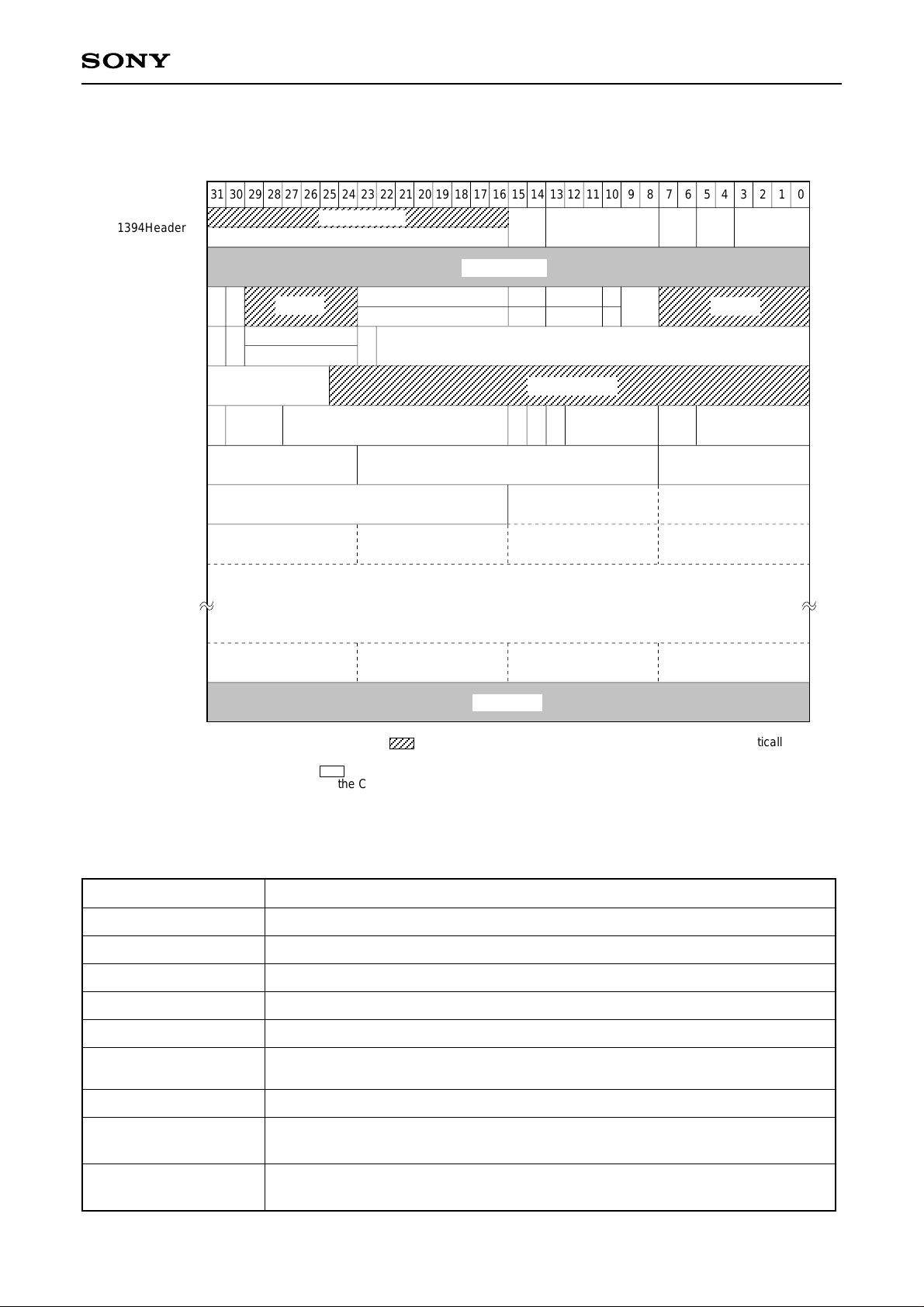
DSS/Isochronous Packet Structure (1 source packet)
SID
FMT
21h
data_length
0098h
DBS FN
09h 10 000
TF
1394Header
CIPHeader1
CIPHeader2
00
10
Header_CRC
QPC
FDF
channel
SPH
1
reserved
reserved
CXD1948R
031302928272625242322212019181716151413121110987654321
speed sytag
DBC
SPHeader
Reserved
TIF
Reserved EF TF UF MS
Reserved Channel Information
data2 data3 data4 data5
data126 data127 data128 data129
Note: The diagonally shaded areas ( ) for 1394Header and CIPHeader1 and 2 are attached automatically by
the CXD1948R. Other areas are set from the external microcomputer via the host I/F.
The white areas ( ) indicate additional data.
In transmission from the CXD1948R to an IEEE 1394PHYIC, the four bits marked "reserved" and "speed"
of the 1394Header are automatically replaced by "tcode".
TimeStamp (27MHz) CR Reserved
Reserved
Data (130 bytes)
Data_CRC
TimeStamp
Reserved
data0 data1
Additional Data Fields
Field Name
TIF
TimeStamp
EF
TF
UF
CR
MS
Channel
Information
Reserved
for bit rate
Description
Time Stamp Invalid Flag 1: Invalid, 0: valid
Time stamp value stamped at 27MHz synchronized to MPEG2 transport stream.
Error Flag 1: Error, 0: No Error
Transition Flag 1: Transition (1sec), 0: No Transition
VBV Underflow Flag 1: Underflow, 0: Normal
Copy Right
Multi/Single 00: Single program, 01: 10: 11: Reserved
– 26 –
Page 27
CXD1948R
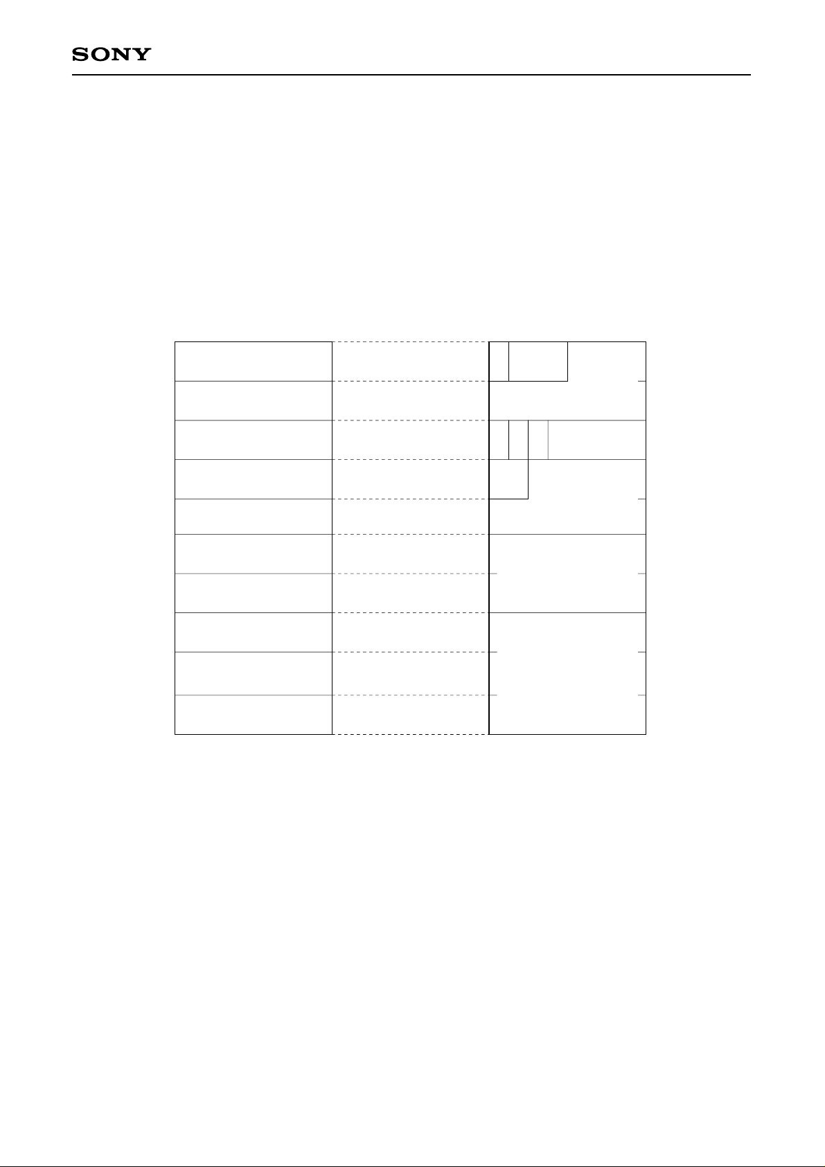
5-6. Relationship between Additional Data and CFR Registers
The CXD1948R has 10 bytes of data registers for additional data. These are common registers for transmit
and receive. Setting is done from the host I/F to add data to the transport stream data.
For receive, the additional data is detected from the isochronous packet and the value is written in.
The relationship between the CFR additional data registers AddData and the additional data in DSS format is
described below.
CFR Registers
MSB LSB
AddData1
AddData2
AddData3
AddData4
AddData5
AddData6
AddData7
AddData8
AddData9
DSS Additional Data
MSB LSB
TIF Reserved
TimeStamp (27MHz)
CREF TF UF
MS
Reserved
Channel Infomation
Reserved
AddData10
5-7. 27MHz Time Stamp
When a 27MHz time stamp synchronized to the transport stream is added on the CXD1948R, the CFR 27MTS
register is set to “1”. Further, a 27MHz clock must be input from the CK27 pin. When the 27MTS register is set
to “0”, the 27MHz time stamp field value enters as is to the lowest 4 bits of the AddData1 register and the value
of the AddData2 register.
– 27 –
Page 28

CXD1948R
5-8. Dummy Packet Transmission
The CXD1948R has a function that automatically transmits a dummy packet when isochronous transmission is
muted, or when there is no packet to be transmitted during isochronous transmission.
The dummy packet consists of header information only. The DBC value is the normal packet value transmitted
on the next isochronous cycle.
Dummy Packet Structure
031302928272625242322212019181716151413121110987654321
1394Header
CIPHeader1
CIPHeader2
data_length
0008h
Header_CRC
0 0 QPC
SID
DBS FN
AA
10
FMT
FDF
channel
SPH
reserved
reserved
speed sytag
DBC
AAA
Data_CRC
Note: The diagonally shaded areas ( ) for 1394Header and CIPHeader1 and 2 are attached automatically by
the CXD1948R. Other areas are set from the external microcomputer via the host I/F.
In transmission from the CXD1948R to an IEEE 1394PHYIC, the four bits marked "reserved" and "speed"
of the 1394Header are automatically replaced by "tcode".
Example of Dummy Packet Transmission (for transmit of 1 data block)
IEEE1394 cycle
DBC = 1 DBC = 2 DBC = 3DBC = 2
Isochronous packet
normal packet dummy packet
– 28 –
Page 29
CXD1948R
5-9. Time Stamp
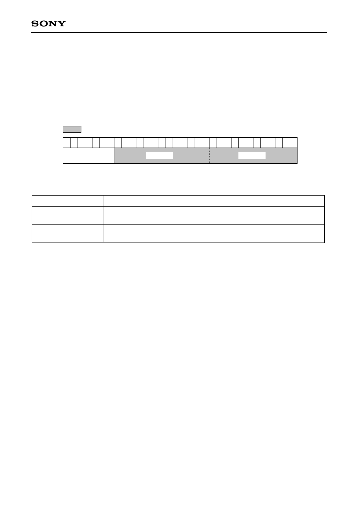
The CXD1948R has a function that adds a time stamp to the input transport stream packet and transmits it,
detects the time stamp on a received packet, and outputs the transport stream packet based on that value. The
time stamp is 25 bits, and is superimposed on the source packet header.
Source Packet Header Structure
time stamp field
031302928272625242322212019181716151413121110987654321
CycleOffsetCycleCountReserved
Time Stamp Field
Field Name
CycleCount
CycleOffset
Time intervals of less than 1 second are expressed in units of 125µs.
(0 to 1F3Fh)
Time intervals of less than 125µs are expressed in units of 24.576MHz clock
cycles. (0 to BFF)
Description
Time Stamp Adding
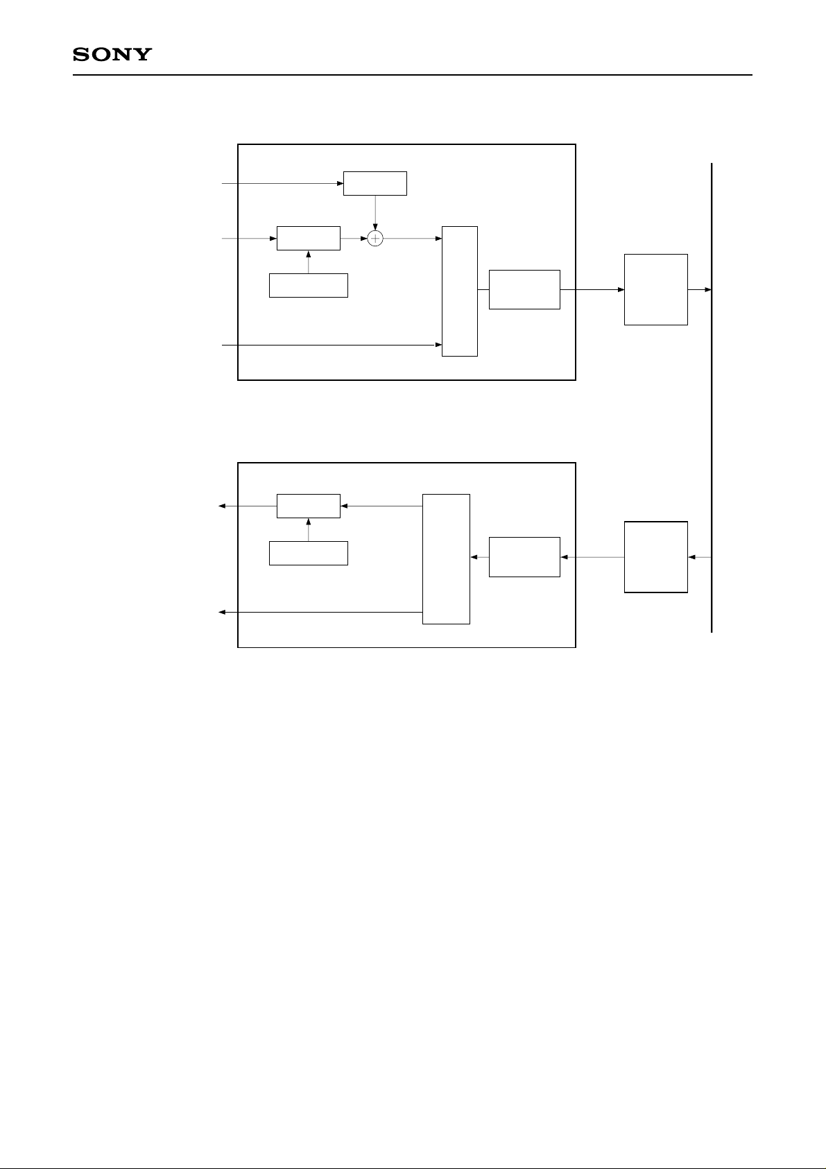
The CXD1948R takes in the internal cycle timer value when the transport stream packet is completely
received. Next it adds the CFR TxDelay register value set from the host I/F to the cycle timer value, and
superimposes it on the source packet header as a time stamp.
Time Stamp Detection
After completely receiving the isochronous packet, the CXD1948R detects the superimposed time stamp to the
source packet header. It compares the detected time stamp value and the internal cycle timer value, and starts
data output from the point where the times match. (Actually output request is performed.)
Also, if the time is already past, it performs data output immediately.
– 29 –
Page 30
Block Diagram
host I/F
CXD1948R (transmit side)
TxDelay
CXD1948R
IEEE1394
Serial BUS
CFR
PACKETEN
transport stream data
transport stream data
DETECT
Cycle Timer
CXD1948R (receive side)
DETECTREADREQ
Cycle Timer
TimeStamp
TimeStamp
MUX
DEMUX
Isochronous
FIFO
Isochronous
FIFO
transmit
data
receive
data
IEEE1394
PHY LSI
IEEE1394
PHY LSI
5-10. Error Processing
When a correct packet can not be received, for example if a CRC error is generated or a packet which violates
protocol is received, the CXD1948R automatically performs error processing.
Error processing control is done by setting the CFR ErrOutEn register.
A description of error processing follows.
Processing for Transmit
ErrFlag input becomes valid when the CFR ErrBit Enable register is set to “1”.
The input error packet is processed in the same way as a normal packet.
However, error information is also transmitted, so only the mode when additional data is added to the transport
stream data is valid. (The superimposed position of the error information is the MSB of the additional data 3rd
byte.)
ErrFlag input becomes invalid when the ErrBitEnable register is set to “0”.
Processing for Receive
ErrFlag output becomes valid when the CFR ErrBit Enable register is set to “1”.
When the received isochronous packet is judged as an error, ErrFlag is made “1” and output.
Because the time stamp cannot be trusted, output is performed immediately.
When the ErrFlagEnable register is set to “0”, only the correctly received isochronous packets are output.
– 30 –
Page 31

CXD1948R
5-11. Late Processing
The CXD1948R automatically performs late processing when an isochronous packet is transmitted.
In late processing, the time stamp superimposed on the source packet header of the packet for transmission is
consulted, and if there is the possibility that the receiving side may not receive the entire packet within the
timing indicated by the time stamp, the packet transmission is canceled.
The time stamp value is the time when the transport stream packet was received plus TxDelay, so the number
of packets for late processing can be reduced by making the TxDelay value larger.
However, the upper limit of the TxDelay value depends on the stream transmission rate and the built-in FIFO
buffer capacity.
6. Asynchronous Communication
6-1. Host/IF
The host I/F controls data communication between the external CPU and the CXD1948R ATF/ARF/CFR/IPB∗1,
respectively.
Communications between the CPU and CXD1948R include:
1) CPU writes data to ATF → asynchronous packet transmit
2) CPU reads data in ARF → asynchronous packet receive
3) CPU writes data to CFR → mode, header data setting
4) CPU reads data in CFR → internal status, header data read-in
5) CXD1948R informs CPU of an interrupt event with an interrupt signal
6) CPU performs insert of isochronous packet from host I/F
7) CPU sets additional information (10 bytes) in isochronous packet
The CXD1948R supports 16-bit and 8-bit host I/F.
The ATF/ARF/CFR built in to the CXD1948R have a 32-bit structure, so all bits can not be accessed with one
access. The target address must be accessed two consecutive times for 16 bits and four consecutive times for
8 bits.
The roles played by the signals communicated between the CXD1948R and the external microcomputer are
given bellow.
DATA [15:0] in/out Data for writing to or reading from specified address
ADDRESS [7:0] in Address for writing or reading data
Data destination (CFR or FIFO) and data breakpoint (Write or Confirm) are
discriminated according to the address
XCS in Access enable from host bus (low active)
XW/R in Data read/write enable signal (high: read; low: write)
XWAIT out Indicates access (read or write) completed to specified address (low active)
XINT out Interrupt signal. Indicates some kind of interrupt when low
Type of interrupt and mask specified by CFR
X8/16 in Host I/F data bus switching
H: 16 bits; L: 8 bits
∗1
ATF (Asynchronous Transmit Fifo), ARF (Asynchronous Receive Fifo),
CFR (Configuration Register), IPB (Insert Packet transmit Buffer)
– 31 –
Page 32
CXD1948R
AAAA
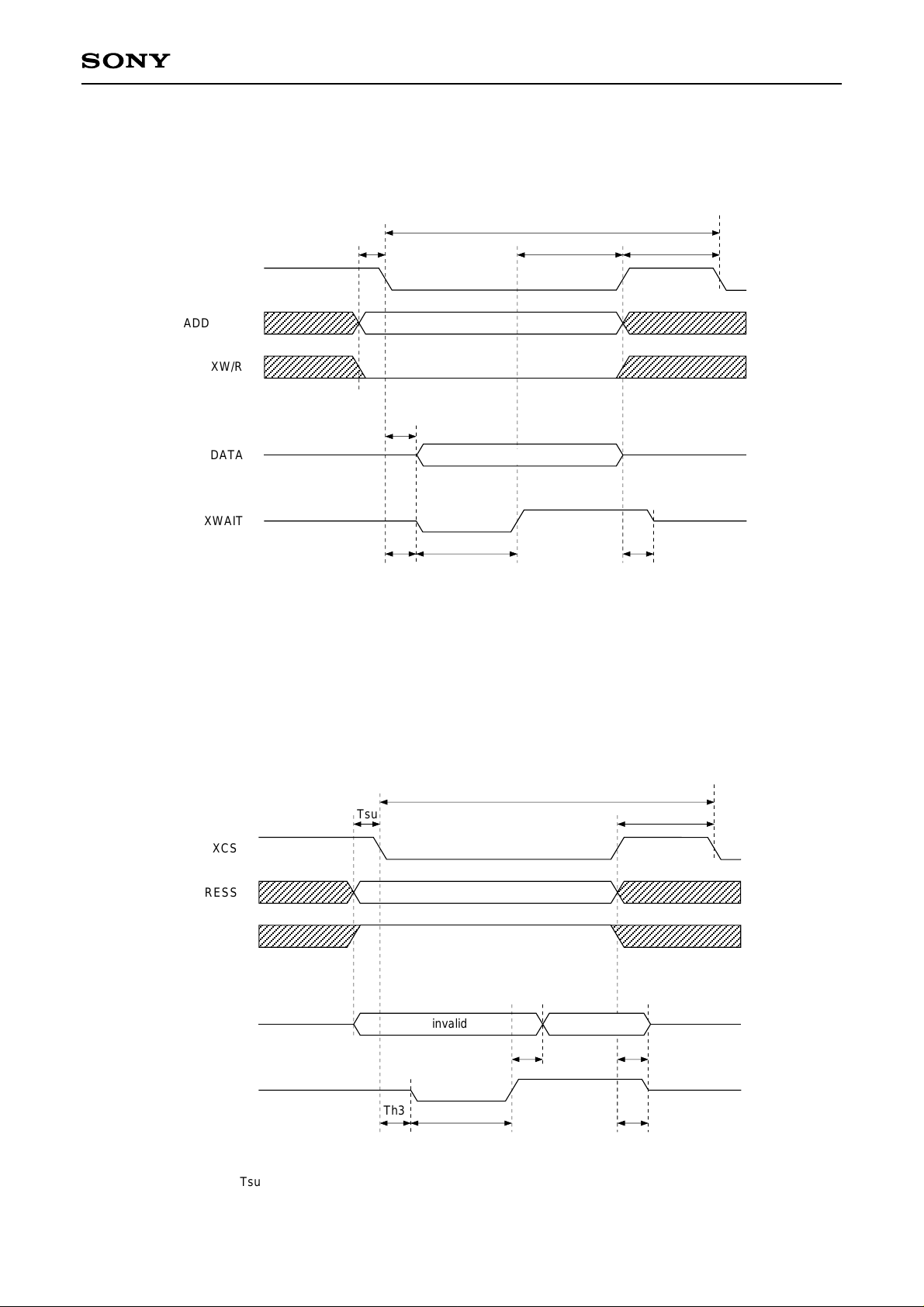
Writing Timing to ATF/CFR/IPF
For write, the CXD1948R latches ADDRESS, XW/R and DATA at XCS falling edge. The timing chart is
illustrated below.
Tcyc
XCS
ADDRESS
XW/R
DATA
Tsu1
Th1
Tsu2
Valid
Tcych
XWAIT
Th2
Tsu1 ≥ 0ns, Tsu2 ≤ 5ns, Th1 ≥ 0ns
Tcyc ≥ 250ns, Tcych ≥ 100ns, Twait ≤ 100ns, Th2 ≤ 5ns, Th3 ≤ 5ns
Twait Th3
Timing for Data Read from ARF/CFR
For read, the CXD1948R latches ADDRESS and XW/R at XCS falling edge. The timing chart is illustrated
below.
Tcyc
Tsu
XCS
ADDRESS
XW/R
Tcych
DATA
XWAIT
Th3
Tsu ≥ 0ns, Th1 ≥ 5ns
Tcyc ≥ 400ns, Tcych ≥ 100ns, Twait ≤ 250ns, Th2 ≤ 5ns, Th3 ≤ 5ns, Th4 ≤ 5ns
invalid
Twait Th4
– 32 –
valid
Th2Th1
Page 33
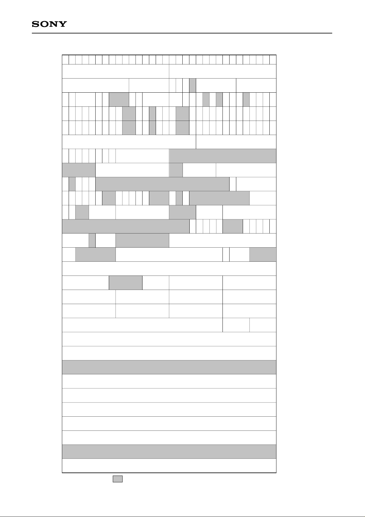
Configuration Register (CFR) Address Map
CXD1948R
31302928272625242322212019181716151413121110987654321
00
04
08
0C
10
14
18
1C
20
24
28
2C
30
34
38
BusNumber NodeNumber
BsyCtrl BlkBusDep ATRC
idVal
RxSld
Int
PhyInt
PhRRx
BusRst
Int
PhyInt
PhRRx
BusRst
IGFOn
HSTxOn
HSRxOn
IGFMode
ArbGp
Arf
ArfAFull
WrPhy
FrGp
ArfDc
4There
EnSp
ArfFull
RdPhy
NOSP NODB
{ 0, 0 }
FairGap
FairGap
IFClear
regRW
AEmpty
Arf
Version
NodeSum CFMContID
AsyncAI
CyMasEn
CySt
IFOvfIFOvf
CySec
CySt
CySec
TxEn
TxRdy
TxRdy
RxEn
RxDta
RxDta
EndSlf
CmdRst
EndSlf
CmdRst
RstTx
RstRx
ITStk
ITStk
ATStk
ATStk
SntRj
SntRj
HdrErr
HdrErr
root
TCErr
TCErr
Status
Power
CyMas
AIDT16
CycleNumber CycleOffset
27MTS
ErrBitEn
ArfEmpty
LPS
RxChannel
TxDelay S_PacketSize
AtfFull
4Avail
Atf
AEmpty
Atf
AtfAFull
AtfEmpty
PacketBanks
ATF
ARF
Clear
Clear
PDIR2
PDIR4
PDIR3
{Tag [1: 0] , ChNumber [5: 0] , 1394Rsv [1: 0 ] , Speed [1: 0 ] , sy [3 :0] }
TxCIPHdr1
{ DBS [7: 0], FN [1: 0], QPC [2: 0], SPH, rsv [1: 0] }
TxCIPHdr2
{ 1, 0, FMT [5 : 0], TF, FDF [22 : 0] }
Revision
ITxC
CyTEn
CyLst
CyPnd
CyDne
CyLst
CyPnd
CyDne
PDIR1
PDIR0
Tx1394Hdr
27MTIF
IRxC
CyAbFail
CyAbFail
DiffGap
PhyDataRxRegPhyAdRxRegPhyRegDataPhyRegAd
27Mrsv
TmsDis
TxLate
IPktLateIPktLate
TxLate
SIGapCnt
PDATA4
StrSid
ErrOutEn
RxLack
IFEmpty
RxLack
IFEmpty
ATAck
PDATA3
PDATA2
0
AckCtl
IPTxGo
IFFull
IsAbFail
IFFull
IsAbFail
PDATA1
PDATA0
Version
Node Address
Control
Interrupt
Interrupt Mask
Cycle Timer
DIF Mode
IsoTxRx Init
Diagnostics
Async Status
Phy Chip Access
Parallel Port
Tx1394Hdr
TxCIPHdr1
TxCIPHdr2
3C
40
44
48
4C
50
64
68
6C
70
74
78
SPH-reserved AddSize AddData2 AddData1
AddData6 AddData5
AddData4 AddData3
AddData8 AddData7AddData10 AddData9
Data_length [15 : 0] , Tag [1 : 0] , ChNumber [5 : 0]
Rx1394Hdr
Rx1394Hdr
tCode [3 : 0]
Rx1394Hdr
sy [3 : 0]
RxCIPHdr1
EOH, form, SID [5 : 0] , DBS [7 : 0] , FN [1 : 0] , QPC [2 : 0] , SPH, rsv [1 : 0] , DBC [7 : 0]
RxCIPHdr2
EOH, form, TF, FMT [5 : 0] , FDF [22 : 0]
IPB Write (first quadlet of the packet)
IPB Write
IPB Write (confirm write)
ATF Write (first quadlet of the packet)
ATF Write/ARF Read
SPH-rsv/AddData1-2
AddData3-6
AddData7-10
Rx1394Hdr
RxCIPHdr1
RxCIPHdr2
7C
ATF Write (confirm write)
Note: The shaded areas ( ) are reserved and can not be used.
– 33 –
Page 34
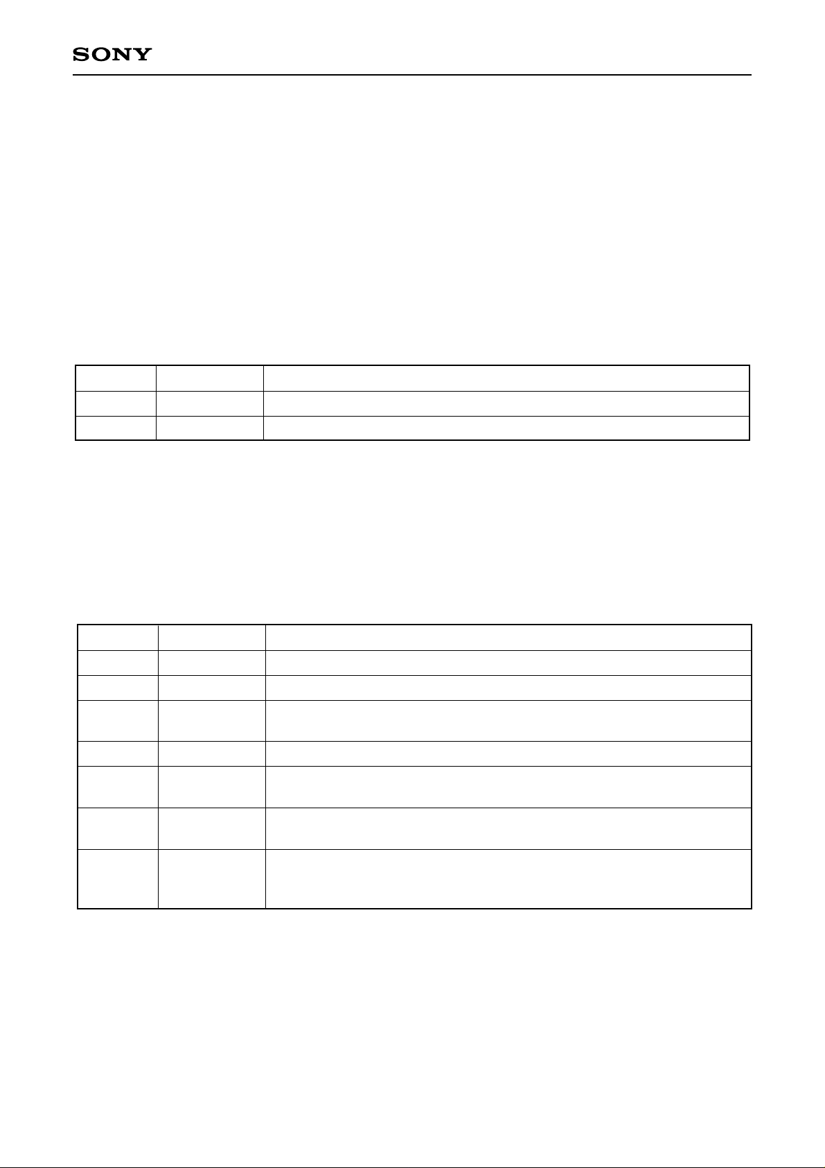
CXD1948R
6-2. CFR (Configuration Register)
This is a memory space to store the status information and operation mode and packet header information
inside the chip. Read/write with the external microcomputer can be performed via the host I/F. (Be sure to set
to “0” when writing to the reserved area.)
The address map and register contents are shown below.
Register Description
1) Version/Revision Register
These registers have the CXD1948R version/revision written in them.
The register address is 00h; they are read only, and the initial value is 0000_0001h.
Bit Name
31 to 16
15 to 0
Version
Revision
CXD1948R Version Number
CXD1948R Revision Number
Function
2) Node Address Register
These registers are used for packet receive/refuse control, and to monitor root/cycle master status and the
total number of nodes connected.
The register address is 04h and the initial value is FFFF_0040h.
Only the bus number is read/write, and the other registers are normally read only, but the diagnostic register
can be read/write by setting regRW to “1”.
Bit Name
31 to 22
21 to 16
15
14
12
Bus Number
Node Number
root
Power Status
CyMst
Bus number of connected bus
Node number of this link
Root/not root for this link
1: root; 0: not root
Cable power status for this mode
Whether or not this link is cycle master
1: cycle master; 0: not
Function
11 to 6
5 to 0
NodeSum
CFMcontID
Total number of connected nodes. Value is 0 when an error occurs in Self_ID
communication.
The Phy_ID of the contender is inserted here. However, when the node can
itself be a contender and it has a larger Phy_ID than this value, then the
node itself is the contender.
– 34 –
Page 35

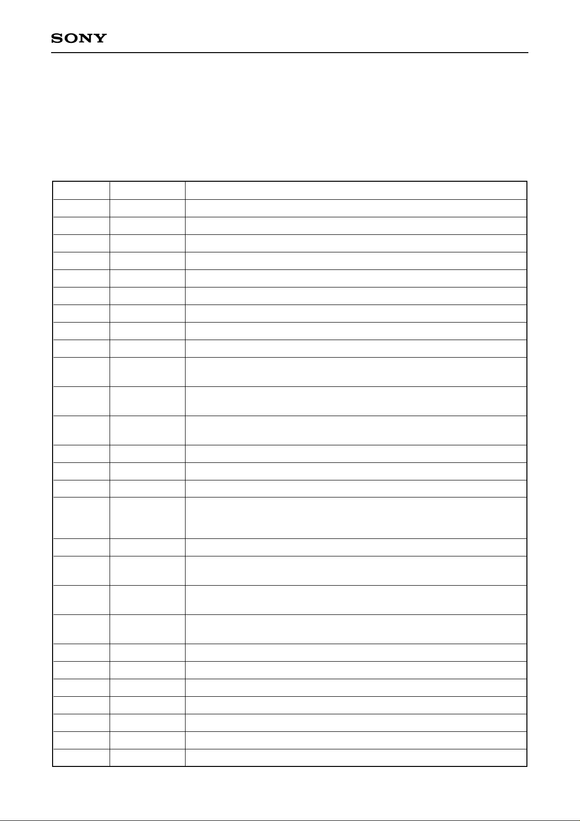
3) Control Register
These registers perform settings for the CXD1948R basic operations.
The register address is 08h; they are read/write, and the initial value is C400_0A00h.
CXD1948R
Bit Name
31
30
29 to 27
26
25
21
20
19 to 16
15, 14
idVal
RxSld
BsyCtrl
TxEn
RxEn
RstTx
RstRx
BlkBusDep
ATRC
Function
Receives packet from the address set in the node address register at “1”.
Receives packet at bus number “3Fh” node number “3fh” only at “0”.
Validates reception of SelfID packet at “1”. Non-valid at “0”.
Processing for NodeSum, CFMContID, DiffGap and SIGapCnt is invalid.
Controls Busy status of input packet.
000 = Returns busy according to normal busy/retry protocol when necessary.
(Always fixed at “000” on the CXD1948R)
Transmitter does not transmit Arbitration and packet when “0”
Receiver does not receive packet when “0”
Sync resets transmitter when set to “1”
This bit is cleared automatically
Sync resets receiver when set to “1”
This bit is cleared automatically
Access limits on Broadcast packets for the CSR bus-dependent area can be
set here. Each bit corresponds to 128 bytes of the CSR bus-dependent area.
With the LSB corresponding to the first 128 bytes, and so on until the MSB
corresponding to the last 128 bytes, access to any area for which the
corresponding bit has been set “1” is invalid.
The Retry Code can be controlled. The Retry Code for the packet being sent
is the logical OR of the value set here and the value stored in ATF.
13
12
11
9
7
6
0
5
3
2
1
AIDT16
AsyncAI
CyMasEn
CyTEn
ITxC
IRxC
AckCtl
TmsDis
StrSid
ErrOutEn
IPTxGo
Selects AIDT bus width. 8 bits at “0” and 16 bits at “1”
Transport stream I/F setting. Synchronous at “0” and asynchronous at “1”.
When “1” and the node becomes the ROOT, Cycle Master functions are activated.
Validates Cycle Offset increment at “1”
Transmits isochronous packet with tCode = C at “1”
Transmits isochronous packet with tCode = A at “0”
Receives tCode = A, tCode = C packets as isochronous packet at “1”
Receives tCode = A packet as isochronous packet at “0”
Controls Ack code which is returned when tCode = 0, 1 (Write request
quadlet/block) packets are received.
0: Ack code = 1 (complate), 1: Ack code = 0 (pending)
Does not use time stamp for data read during receive at “1”
Uses time stamp for data read during receive at “0”
Takes received SelfID packet in to ARF at “1”
Does not take received SelfID packet in to ARF at “0”
Outputs error packet at ErrFlag High during receive at “1”
Does not output error packet during receive at “0”
Transmits insert packet at “1”
Automatically changes to “0” after transmit
– 35 –
Page 36
CXD1948R
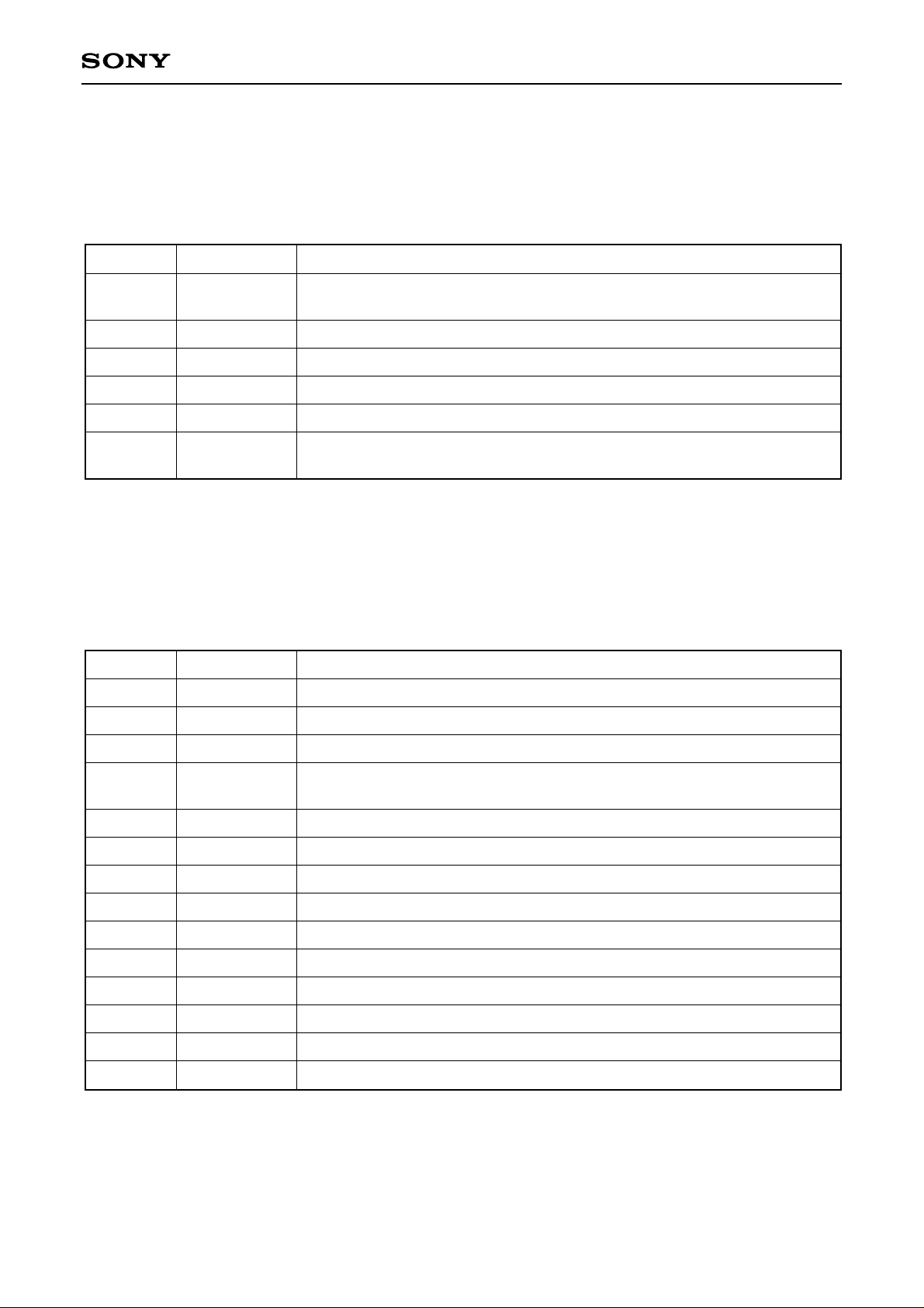
4) Interrupt and Interrupt-Mask Registers
These registers combine the Interrupt Register, which informs the host I/F of changes in the CXD1948R status,
and the Interrupt Mask Register, which masks the Interrupt Register.
The address of the Interrupt Register is 0Ch, and when the regRW bit is “0”, bits other than Int bit are cleared
by writing. When the regRW bit is “1” all bits are read/write.
The address of the Interrupt-Mask Register is 10H and it is read/write.
The initial value for both registers is 0000_0000h.
Bit Name
31
30
29
28
27
26
25
24
23
20
19
17
16
15
Int
PhyInt
PhRRx
BusRst
FairGap
TxRdy
RxDta
CmdRst
EndSlf
ITStk
ATStk
SntRj
HdrErr
TCErr
Function
Indicates the OR result of all the interrupt (interrupt mask) bits.
Indicates Phy Interrupt received from Phy chip
Indicates data received from Phy to Phy register
Indicates Bus Reset received from Phy
Indicates FairGap received from Phy
Transmitter is able to transmit
Receiver has received a correct packet
Receiver has received a packet addressed to CSR RESET_START register
SelfID phase complete
Transmitter detected wrong data in isochronous FIFO during isochronous
transmit
Transmitter detected wrong data in asynchronous FIFO during asynchronous
transmit
Receiver transmitted Busy Ack for a packet transmitted to this node because
receive FIFO is full
Receiver detected Header CRC error in the packet transmitted to this node
Transmitter detected wrong tCode data in transmit FIFO
12
11
10
9
8
7
6
5
4
3
2
1
0
IFOvf
CySec
CySt
CyDne
CyPnd
CyLst
CyAbFail
IPktLate
TxLate
RxLack
IFEmpty
IFFull
IsAbFail
Indicates overflow in isochronous FIFO
I
ndicates that Cycle Timer register Cycle Number upper 7 bits were
incremented.
(This is generated almost every second when Cycle Timer is valid.)
Transmitter/Receiver transmitted/received Cycle Start packet
After transmit or receive of Cycle Start packet, FairGap was detected on the
bus. This means that the isochronous cycle is complete.
Indicates that Cycle Timer register Cycle Offset is “0”. Stays as is until
isochronous cycle is complete.
When not Cycle Master, indicates that Cycle Timer completed 2 cycles
without receiving Cycle Start packet.
Failure of Cycle Start packet transmission Arbitration
Late transmit of insert packet
Late transmit of isochronous packet
Indicates isochronous packet non-continuous DBC
Isochronous FIFO empty
Isochronous FIFO full
Failure of isochronous packet transmission Arbitration
– 36 –
Page 37

CXD1948R
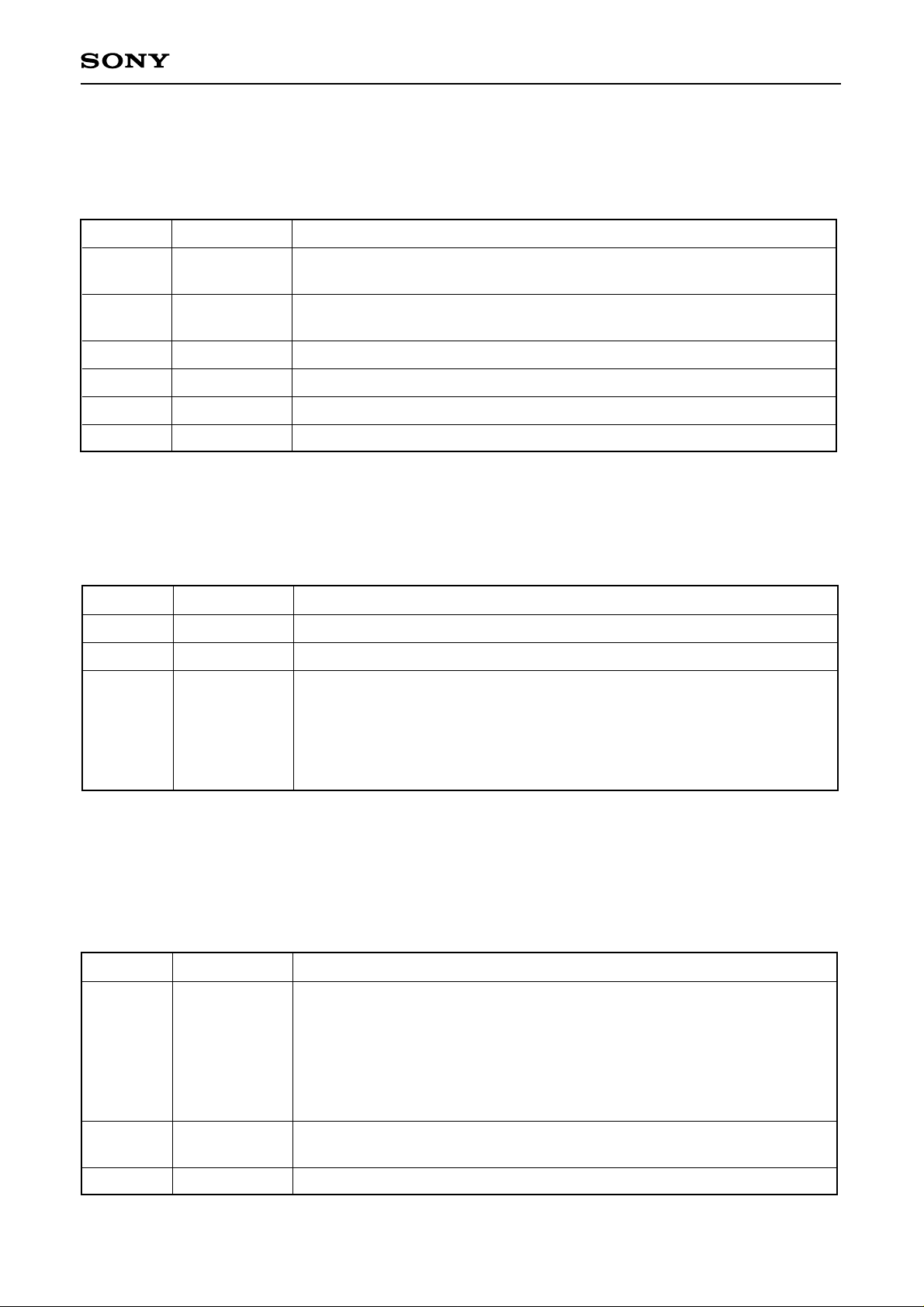
5) Cycle Timer Registers
These registers are composed of the 24.576MHz clock cycle Cycle Offset and the 125µs in its host, and the
Cycle Master that counts 1 second. The value of all nodes are regulated by the Cycle Master node.
The register address is 14h; it is read/write, and the initial value is 0000_0000h.
Bit Name
Function
The upper 7 bits counts seconds (1Hz) and the lower 13 bits count the
31 to 12
CycleNumber
isochronous cycle (8kHz = 125µs). The values are controlled by Control
register Cycle Master and Cycle Timer Enable.
Counts the system clock (24.576MHz). The Cycle Number is incremented
11 to 0
CycleOffset
when this counter completes one cycle. The value is controlled by Control
register Cycle Master and Cycle Timer Enable.
6) DIF Mode Register
This register performs settings for transmit and receive of isochronous packets, and sets transmitted
isochronous packet 1394 header information (specified in the Draft).
The register address is 18h; it is read/write, and the initial value is 0100_0000h.
Bit
31
30
29
28
27
26
25
24
Name
IGFOn
IGFMode
HSTxOn
HSRxOn
IFClear
ErrBitEn
27MTS
LPS
Isochronous FIFO operation is active at “1”
Changes isochronous FIFO operation to transmit at “1”. Receives at “0”
Isochronous transmit side operation is active at “1”. Invalid at “0”
Isochronous receive side operation is active at “1”. Invalid at “0”
Clears isochronous FIFO at “1”
Uses 27MHz time stamp at “1”
Does not use 27MHz time stamp at “0”
LPS pin high at “1”
LPS pin low at “0”
Function
23 to 16
RxChannel
Tag/Channel Number for isochronous packet receive
7) IsoTxRx Init
This register performs setting related to isochronous packet transmit/receive time stamp, and packet size and
packet bank.
The register address is 1Ch; it is read/write, and the initial value is 0000_0000h.
Bit Name
Function
Transmission delay time for isochronous packets. The upper 6 bits are
26 to 16
TxDelay
added to the lower 6 bits of the Cycle Number, and the lower 5 bits are
added to the upper 5 bits of the Cycle Offset to obtain the time stamp.
13 to 9
8 to 0
PacketBanks
S_PacketSize
Sets number of isochronous FIFO packet bank
Sets isochronous packet source packet size
The value includes SPH and additional data (byte units)
– 37 –
Page 38
CXD1948R
8) Diagnostic Register
This register controls or monitors the CXD1948R status.
The register address is 20h and the initial value is 0000_0000h.
Only the EnSp bit and regRW bit are read/write; other bits are read/write when the regRW bit is “1” and read
only when it is “0”.
Bit Name
31
29
28
27
6
5 to 0
EnSp
ArbGp
FrGp
regRW
DiffGap
SIGapCnt
Receives all packets on the bus regardless of receiver address and format
at “1”. Invalid at “0”.
Bus is in idle state due to Arbitration Reset Gap
Bus is in idle state due to Fair Gap
Almost all registers are read/write when set at “1”
“1” when there is dispersion in Gap count values in received Self ID
This value is entered when all Gap count values in received Self ID are the
same. “00h” when bus reset is generated.
Function
9) Asynchronous Transmit and Receive FIFO Status Registers
These registers can monitor and control the ATF/ARF statuses.
The register address is 24h and the initial value is 0428_0000h.
Only the ClearATF bit and ClearARF bit are read/write; other bits are read/write when the regRW bit is “1” and
read only when it is “0”.
Bit Name
31
ARFFull
ARF is full when “1” and receive is not possible
Function
30
29
28
27
26
23
22
21
20
19
15
13
3 to 0
ARFAFull
ARF4Th
ARFDc
ARFAEmpty
ARFEmpty
ATFFull
ATFAFull
ATF4Avail
ATFAEmpty
ATFEmpty
ClearATF
ClearARF
ATAck
ARF can receive only one more quadlet when “1”
More than 4 quadlets of data are written in ARF when “1”
This is the control bit for reading a packet from ARF, and is “1” only when the
first and last quadlets of the packet are read.
Only one more quadlet of data is written in ARF when “1”
ARF is empty when “1” and there is no data to be read
ATF is full when “1” and write is not possible
ATF can write only one more quadlet when “1”
More than 4 quadlets of data can be written in ATF when “1”
ATF has only one more quadlet of data not transmitted when “1”
ATF is empty when “1” and there is no data for transmit
Sync reset of ATF when “1” (Self Clear)
Sync reset of ARF when “1” (Self Clear)
Value of received Ack code
– 38 –
Page 39
CXD1948R
10) Phy Chip Access Registers
These registers are used for read/write of the contents of the Phy chip Phy register connected to the
CXD1948R.
The register address is 28h and the initial value is 0000_0000h.
Bit Name
31
30
27 to 24
23 to 16
11 to 8
7 to 0
RdPhy
WrPhy
PhyRegAd
PhyRegData
PhyAdRxReg
PhyDataRxReg
The CXD1948R requests read to the address set in PhyRegAd via the Phy
I/F when “1”
The CXD1948R requests write to the address set in PhyRegAd via the Phy
I/F when “1”
Sets the read/write address of the connected Phy chip Phy register
Value of data for write to address specified by PhyRegAd
Value of read Phy register address during read
Value of the read Phy register data during read
Function
11) Tx1394Hdr Registers
These registers are used to set the value of 1394Hdr added at the CXD1948R during isochronous transmit,
and the number of data blocks transmitted in the isochronous cycle.
The register address is 30h and the initial value is 0000_0000h.
Bit Name
31 to 28
26 to 24
NOSP
NODB
Sets number of source packets transmitted in the isochronous cycle
Sets number of data blocks transmitted in the isochronous cycle
Function
Header when transmitting isochronous packet
bit15 to bit14: Tag [1 : 0], Isochronous data format tag
15 to 0
Tx1394Hdr
bit13 to bit8: ChNumber [5 : 0], Isochronous Channel
bit7 to bit6: Rsv [1 : 0], Reserved
bit5 to bit4: Speed [1 : 0], Speed code
bit3 to bit0: Sy [3 : 0], Synchronization Code
12) TxCIPHdr1 Registers
These registers are used to set the value of CIPHdr1 added at the CXD1948R during isochronous
transmission and settings related to the 27MHz time stamp.
CIPHdr1 is one of the CIP headers.
The register address is 34h and the initial value is 0000_0070h.
Bit Name
Function
Value of CIPHdr1 added during isochronous transmit
bit31 to bit30: “00”
bit23 to bit16: DBS, one data block size (quadlet)
23 to 8
TxCIPHdr1
bit15 to bit14: FN [1 : 0], Franction number
bit13 to bit11: QPC [2 : 0], Quadlet padding Count
bit10: SPH, Source packet Header
bit9 to bit8: rsv [1 : 0] reserved
7
6 to 4
27MTIF
27Mrsv
27MHz time stamp value invalid at “1”
27MHz time stamp value valid at “0”
Reserve area when 27MHz time stamp is used
– 39 –
Page 40
CXD1948R
13) TxCIPHdr2 Registers
These registers are used to set the value of CIPHdr2 added at the CXD1948R during isochronous
transmission. CIPHdr2 is one of the CIP headers.
The register address is 38h and the initial value is 0000_0000h.
Bit Name
Function
Value of CIPHdr2 added during isochronous transmit
bit31 to bit30: “10”
31 to 16
TxCIPHdr2
bit29 to bit24: FMT [5 : 0], Format ID
bit23: TF, Time Shift 1: TimeShift
0: no TimeShift
bit22 to bit0: Format Dependet Field
14) SPH-reserved/AddData1, 2 Registers
These registers are used for setting the reserve value of the source packet header added/detected by the
CXD1948R during isochronous communication, and for setting and storing additional data and setting the
number of additional data.
The register address is 3Ch and the initial value is 0000_0000h.
Bit Name
31 to 25
19 to 16
15 to 8
7 to 0
SPH-reserved
AddSize
AddData1
AddData2
Value of source packet header reserve stored during receive or added during
isochronous communication
Sets number of data added during isochronous transmission
Value of data 1 stored during receive or added during isochronous communication
Value of data 2 stored during receive or added during isochronous communication
Function
15) AddData3 to 6 Registers
These registers are used for the data added/detected by the CXD1948R during isochronous communication.
The register address is 40h and the initial value is 0000_0000h.
Bit Name
31 to 24
23 to 16
15 to 8
7 to 0
AddData3
AddData4
AddData5
AddData6
Value of data 3 stored during receive or added during isochronous communication
Value of data 4 stored during receive or added during isochronous communication
Value of data 5 stored during receive or added during isochronous communication
Value of data 6 stored during receive or added during isochronous communication
Function
16) AddData7 to 10 Registers
These registers are used for the data added/detected by the CXD1948R during isochronous communication.
The register address is 44h and the initial value is 0000_0000h.
Bit Name
31 to 24
23 to 16
15 to 8
AddData7
AddData8
AddData9
Value of data 7 stored during receive or added during isochronous communication
Value of data 8 stored during receive or added during isochronous communication
Value of data 9 stored during receive or added during isochronous communication
Function
7 to 0
AddData10
Value of data 10 stored during receive or added during isochronous communication
– 40 –
Page 41

CXD1948R
17) Rx1394Hdr Registers
These registers are used to store the value of the 1394Hdr detected by the CXD1948R during isochronous
receive.
The register address is 48h and the initial value is 0000_0000h.
Bit Name
Function
Value of 1394Hdr detected during isochronous receive
bit31 to bit16: Data_length [15 : 0], 1 isochronous packet byte length
31 to 8
Rx1394Hdr
3 to 0
bit15, bit14: Tag [1 : 0], Isochronous data format tage
bit13 to bit8: ChNumber [5 : 0], Isochronous channel Number
bit7 to bit4: tCode [3 : 0], Isochronous Transaction code
bit3 to bit0: sy [3 : 0] Synchronization Code
18) RxCIPHdr1 Registers
These registers are used to store the value of the CIPHdr1 detected by the CXD1948R during isochronous
receive.
The register address is 4Ch and the initial value is 0000_0000h.
Bit Name
Function
Value of CIPHdr1 detected during isochronous receive
bit31: EOH
bit30: form
bit29 to bit24: SID, Source [5 : 0] Node ID
31 to 0
RxCIPHdr1
bit23 to bit16: DBS [7 : 0], Data Block Size
bit15, bit14: FN [1 : 0] Fraction
bit13 to bit11: QPC [2 : 0], Quadlet Padding Count
bit10: SPH, Source Packet Header
bit9, bit8: rsv [1 : 0], Reserved
bit7 to bit0: DBC [7 : 0], Data Block Counter
19) RxCIPHdr2 Registers
These registers are used to store the value of the CIPHdr2 detected by the CXD1948R during isochronous
receive.
The register address is 50h and the initial value is 0000_0000h.
Bit Name
Function
Value of CIPHdr2 detected during isochronous receive
bit31: EOH
31 to 0
RxCIPHdr2
bit30: form
bit29 to bit24: FMT [5 : 0], Format ID
bit23: TF, TimeShift Flag
bit22 to bit0: FDF [22 : 0], Format Dependent on Fields
20) IPBWrite (first quadlet of the packet) Registers
The first quadlet of the transmitted insert packet is written in these registers.
The register address is 64h and the initial value is 0000_0000h.
Bit Name
Function
IPBWrite
31 to 0
(first quadlet of
Writes the first quadlet of the transmitted insert packet.
the packet)
– 41 –
Page 42

CXD1948R
21) IPBWrite Registers
The second through the next to the last quadlets of the transmitted insert packet are written in these registers.
The register address is 68h and the initial value is 0000_0000h.
Bit Name
31 to 0
IPBWrite
Writes the second through the next to the last quadlets of the transmitted
insert packet.
Function
22) IPBWrite (confirm write) Registers
The last quadlet of the transmitted insert packet is written in these registers.
The register address is 6Ch and the initial value is 0000_0000h.
Bit Name
31 to 0
IPBWrite
(confirm write)
Writes the last quadlet of the transmitted insert packet.
Function
23) ATFWrite (first quadlet of the packet) Registers
The first quadlet of the transmitted asynchronous packet is written in these registers.
The register address is 70h and the initial value is 0000_0000h.
Bit Name
Function
ATFWrite
31 to 0
(first quadlet of
Writes the first quadlet of the transmitted asynchronous packet.
the packet)
24) ATFWrite/ARFRead Registers
The second through the next to the last quadlets of the transmitted asynchronous packet are written in these
registers. Also, the asynchronous packet read from the ARF during receive is read one quadlet at a time.
The register address is 74h and the initial value is 0000_0000h.
Bit Name
31 to 0
ATFWrite
/ARFRead
Transmit: Writes the second through the next to the last quadlets of the
transmitted asynchronous packet.
Receive: Writes the asynchronous packet read from ARF one quadlet at a time.
Function
25) ARFWrite (confirm write) Registers
The last quadlet of the transmitted asynchronous packet is written in these registers.
The register address is 7Ch and the initial value is 0000_0000h.
Bit Name
31 to 0
ATFWrite
(confirm write)
Writes the last quadlet of the transmitted asynchronous packet.
Function
– 42 –
Page 43
26) Parallel Port Registers
These registers are used to set the parallel port I/O direction and data.
The register address is 2Ch and the initial value is 0000_0000h.
Be sure to set all non-pertinent registers to “0”.
Bit Name Function
CXD1948R
12
11
10
9
8
4
3
2
1
0
PDIR4
PDIR3
PDIR2
PDIR1
PDIR0
PDATA4
PDATA3
PDATA2
PDATA1
PDATA0
PORT4 I/O switching setting. 0: Input, 1: Output
PORT3 I/O switching setting. 0: Input, 1: Output
PORT2 I/O switching setting. 0: Input, 1: Output
PORT1 I/O switching setting. 0: Input, 1: Output
PORT0 I/O switching setting. 0: Input, 1: Output
Sets the PORT4 output data when PDIR4 is 0.
Inputs the PORT4 input data when PDIR4 is 1.
Sets the PORT3 output data when PDIR3 is 0.
Inputs the PORT3 input data when PDIR3 is 1.
Sets the PORT2 output data when PDIR2 is 0.
Inputs the PORT2 input data when PDIR2 is 1.
Sets the PORT1 output data when PDIR1 is 0.
Inputs the PORT1 input data when PDIR1 is 1.
Sets the PORT0 output data when PDIR0 is 0.
Inputs the PORT0 input data when PDIR0 is 1.
– 43 –
Page 44
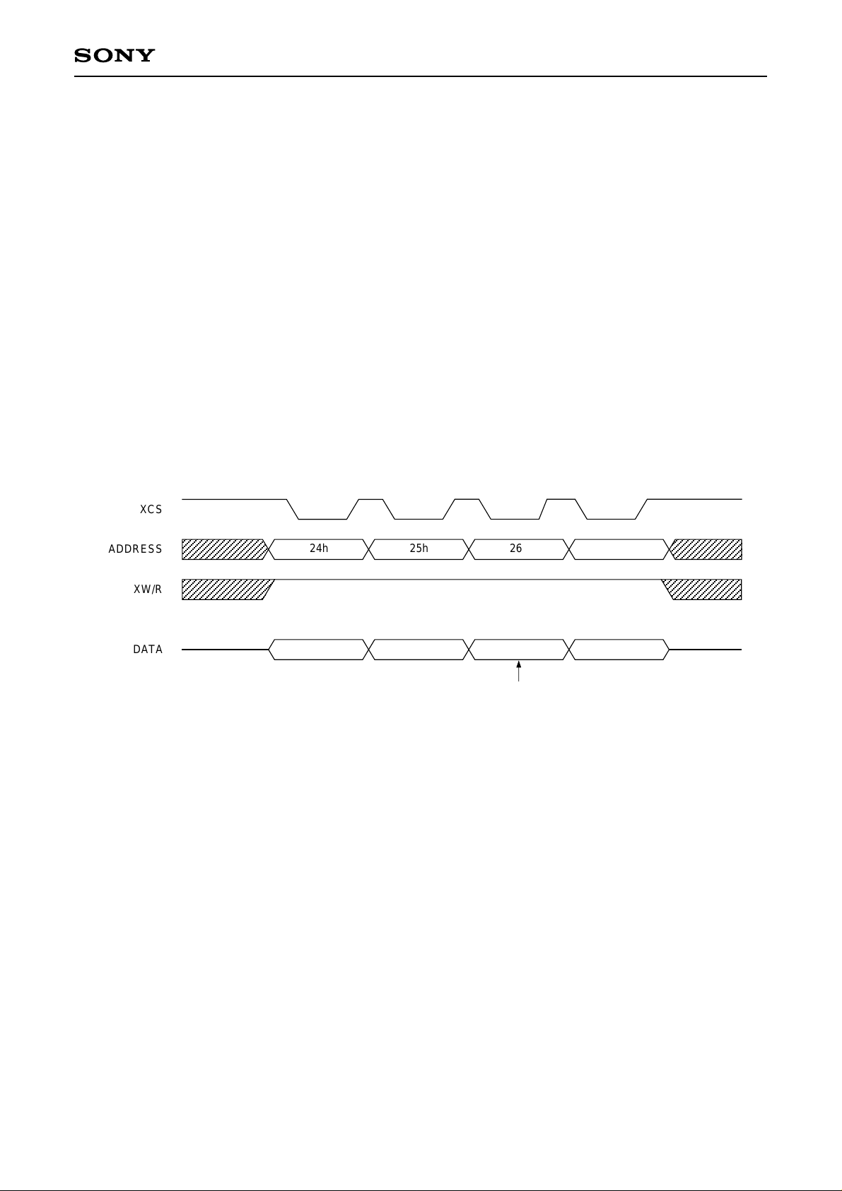
CXD1948R
6-3. Asynchronous Packet Transmission
Packet data is written from the external microcomputer to the ATF inside the CXD1948R in order to transmit an
asynchronous packet. At this time the first quadlet of the packet only is written in the CFR ATFWrite (first
quadlet of the packet) register (70h). The second through the next to the last quadlets are written in the CFR
ATFWrite/ARFRread registers (74h). Then the last quadlet is written in the CFR ATFWrite (confirm write)
register (7Ch) and the packet is stored in the ATF.
However, if the ATF is full, write will not actually be performed even when write is executed.
Once the bus is enabled, transmit takes place automatically.
The procedure for transmitting a quadlet write request packet is given here as an example.
(for 8-bit data interface)
(1) Confirming that ATF is not full
The CFR Async Status register (24h to 27h) is read to confirm that the 23rd bit (AtfFull bit) is low. If it is high it
means that there are some unsent packets stored and it waits until they are transmitted.
XCS
ADDRESS
XW/R
DATA
24h
25h 26h 27h
28h
This indicates that ATF is empty.
It is “80h” when ATF is full.
The number of quadlets that can be stored in ATF can be found from the value of the Async Status register
bits [23 : 19]. The following six states can be found, so a judgement must be made as to whether write is
possible from the number of quadlets in the packet being sent from the external microcomputer.
AtfFull = High: Can’t write
AtfAFull = High: only 1 quadlet
All bits low: 2 to 3 quadlet
Atf4Avail = High: 4 to 28 quadlet
Atf4Avail = High, AtfAEmpty = High: 29 quadlet
Atf4Avail = High, AtfEmpty = High: 30 quadlet
– 44 –
Page 45
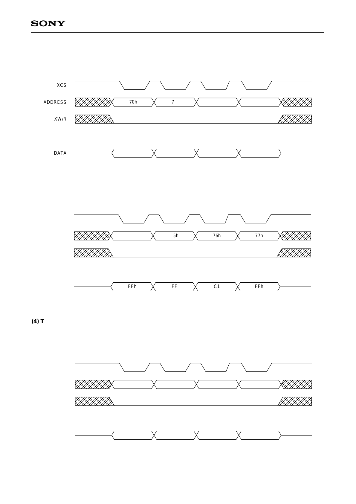
(2) First quadlet of the transmitted packet Write
Let the first quadlet of the quadlet write request packet be “00000000h”.
This is written in the CFR ATFWrite (first quadlet of the packet) register.
XCS
CXD1948R
ADDRESS
XW/R
DATA
70h
00h 00h 00h 00h
71h 72h 73h
(3) Second quadlet of the transmitted packet Write
Let the second quadlet of the quadlet write request packet be “FFC1FFFFh”.
This is written in the CFR ATFWrite/ARFRead register.
XCS
ADDRESS
XW/R
74h
75h 76h 77h
DATA
FFh FF C1 FFh
(4) Third quadlet of the transmitted packet Write
Let the third quadlet of the quadlet write request packet be “F000000Ch”.
This is written in the CFR ATFWrite/ARFRead register.
XCS
ADDRESS
XW/R
DATA
74h 75h 76h 77h
0Ch 00h 00h F0h
– 45 –
Page 46

(5) Last quadlet of the transmitted packet Write
Let the last quadlet of the quadlet write request packet be “12345678h”.
This is written in the CFR ATFWrite (confirm write) register.
XCS
CXD1948R
ADDRESS
XW/R
DATA
7Ch 7Dh 7Eh 7Fh
78h 56h 34h 12h
The quadlet write request packet is stored in the ATF as shown above. When the bus is enabled, the
CXD1948R transmits automatically. If transmit does not take place, the CFR interrupt register (0Ch to 0Fh)
must be read to confirm if the ATStk bit or TCErr bit is high. If these bits are high, the packet stored in the ATF
may not be correct.
ATStk = High: If the first quadlet of the packet was not written in the CFR ATFWrite (first quadlet of the
packet) register but was written in the ATFWrite/ARFRead register or the ATFWrite (confirm
write) register.
TCErr = High: A value that is not a transaction code able to be transmitted by asynchronous packet is
written in the tCode field of the first quadlet of the packet.
The transactions codes that can be transmitted as asynchronous packets are any of (0, 1, 2,
4, 5, 6, 7, 9, B, Eh).
For either of ATStk or TCErr above, the next packet for write will not be transmitted even if it is correct.
At this time “1” must be written in the Async Status register ClearATF bit in order to clear the ATF. Transmit is
then enabled when a correct packet is written.
– 46 –
Page 47
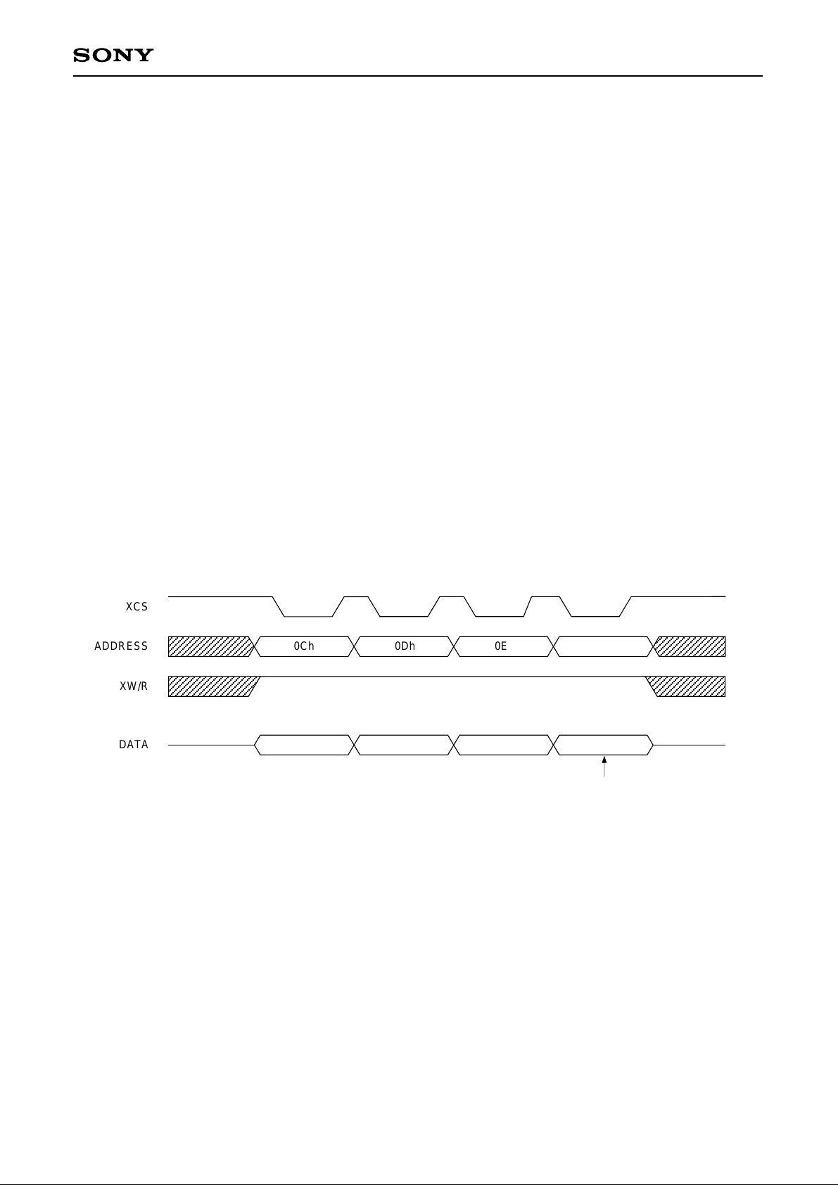
CXD1948R
6-4. Asynchronous Packet Reception
Basically, if there is room to write the packet in FIFO and the destination_ID matches, then asynchronous
packets are received. Receive is completed when the packet data is read from the ARF inside the CXD1948R
by the external microcomputer.
The CXD1948R raises an RxDta flag when a packet is received. (Normally, if the RxDta bit of the CFR
Interrupt Mask register (10h to 14h) is set at “1”, XINT goes low when a packet is received and this can be
detected.)
Next, the CFR Async Status register (24h to 28h) ArfEmpty bit should be low. This indicates that a correct
packet was received.
After this, one quadlet at a time can be read by reading the CFR ATFWrite/ARFRead registers (74h to 78h).
Packet receive is completed by repeating this until the ArfEmpty bit goes high.
However, if the ARF status is empty, read will not be done even if Read is executed. In this case, the data read
by the microcomputer will be the previously read value.
The procedure for receiving a quadlet write request packet is given here as an example.
(for 8-bit data interface)
(1) Confirming that the packet was received
The CFR Interrupt register (0Ch to 0Fh) is read to confirm that the 25th bit (RxDta bit) is high.
XCS
ADDRESS
XW/R
DATA
0Ch
0Dh 0Eh 0Fh
82h
This indicates that RxDta only was generated.
(2) Confirming that the received packet was stored correctly in FIFO
The CFR Async Status register (24h to 27h) is read to confirm that the 26th bit (ArfEmpty bit) is low.
If this bit is high it means that reception may be in progress (all quadlets have not arrived). Read can not be
done in this state, so wait and then clear again.
– 47 –
Page 48
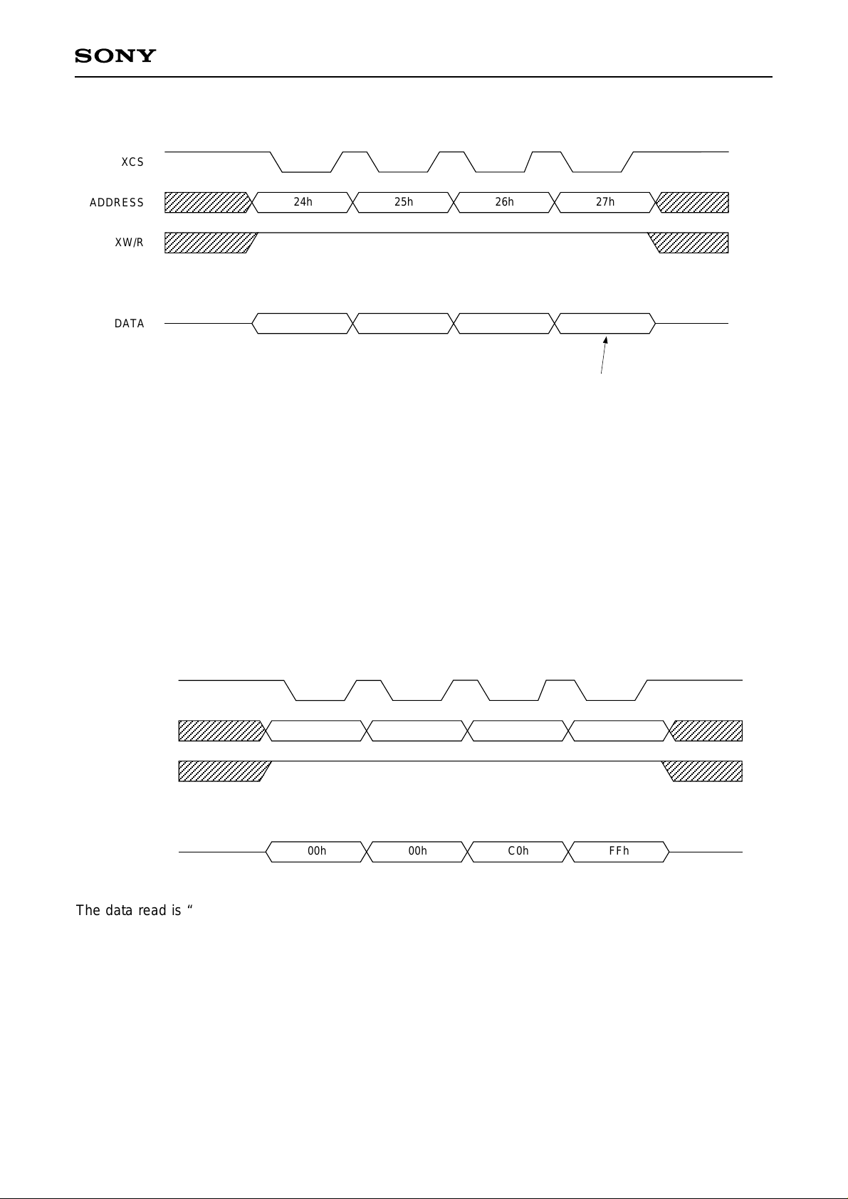
XCS
CXD1948R
ADDRESS
XW/R
DATA
24h
25h 26h 27h
20h
This indicates ARF4There flags up.
In the above example, the Arf4There are high and ArfEmpty is low.
This means that the packet stored in FIFO has more than 4 quadlets, including the footer (quadlet to which the
Link that received the packet is added automatically; speed and ackSent, etc. are written).
ArfDc is “1” only when the read quadlet is a start quadlet or a footer of packet.
The read quadlet can be identified whether it is a start quadlet or a footer by confirming the ArfDc bit of the
Async Status register (24h to 27h) after reading the qualet.
(3) First quadlet of the received packet Read
The CFR ATFWrite/ARFRead register is read.
XCS
ADDRESS
XW/R
DATA
74h
00h 00h C0h FFh
75h 76h 77h
The data read is “FFC00000h”. The read quadlet can be identified as a start quadlet by confirming the ArfDc
bit of the Async Status register (24h to 27h) after reading the qualet.
– 48 –
Page 49

CXD1948R
(4) Second quadlet of the received packet Read
The CFR ATFWrite/ARFRead register is read. As in (2) before, when the status is read after this read, the
ArfDc bit should be low.
XCS
ADDRESS
XW/R
DATA
74h 75h 76h 77h
FFh FFh C1h FFh
(5) Third quadlet of the received packet Read
The CFR ATFWrite/ARFRead register is read.
XCS
ADDRESS
XW/R
74h 75h 76h 77h
DATA
20h 02h 00h F0h
The data read is “F0000220h”.
(6) Fourth quadlet of the received packet Read
The CFR ATFWrite/ARFRead register is read.
XCS
ADDRESS
XW/R
DATA
74h 75h 76h 77h
78h 56h 34h 12h
The data read is “12345678h”.
– 49 –
Page 50
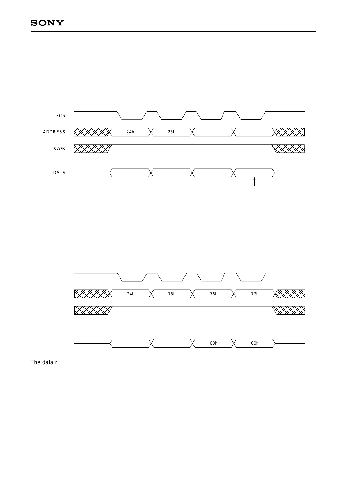
CXD1948R
(7) Checking for remaining packets still in FIFO
4 quadlets were read in preceding items (1) to (6). They were read continuously because Arf4There was high.
If Arf4There was low, Async Status must be read after 1 quadlet is read, to find out if ArfEmpty is high.
Even if Arf4There is high, as in this case, after the 4th quadlet read must be done while checking ArfEmpty in
the same way.
XCS
ADDRESS
XW/R
DATA
24h
25h 26h 27h
08h
This indicates that the ARF Dc flag is up,
and ARF is AlmostEmpty.
In the above example the Arf4There bit is low, so a maximum of 3 more quadlets can be predicted, but the
ArfAEmpty bit is high, so there is only one more quadlet in FIFO. Therefore, the probability is high where the
quadlet to be read next is a footer.
(8) Fifth quadlet of the received packet Read
The CFR ATFWrite/ARFRead register is read.
XCS
ADDRESS
74h 75h 76h 77h
XW/R
DATA
01h 00h 00h 00h
The data read is “00000001h”.
The lower 4 bits of this quadlet are the ackSent field, and this indicates “01h” transmitted as this packet’s
Ack_code. This is always written even if the packet is one which does not have Ack_code transmitted, such as
a broadcast packet.
If this value is “04h”, the ARF may have become full during receive and quadlets may be missing.
If it is “0Dh”, an error was detected in the data field CRC check of the received packet, or data_length and the
actual data length do not match.
– 50 –
Page 51

CXD1948R
(9) Checking for remaining packets still in FIFO
The last quadlet was read in (8) before, so there should be no more packets in FIFO. In addition, it is
confirmed whether the quadlet read last is a footer at the same time.
XCS
ADDRESS
XW/R
DATA
24h
25h 26h 27h
14h
This indicates that ARF Dc flag is up,
and ARF are Empty.
As seen above, it can be confirmed that ARF is Empty and the quadlet read last is a footer.
This completes asynchronous packet reception.
– 51 –
Page 52
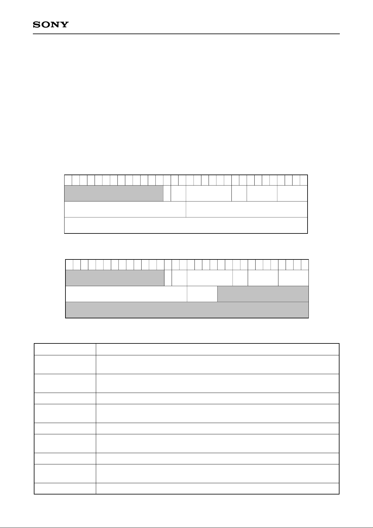
CXD1948R
6-5. CXD1948R Data Format
6-5-1. Asynchronous Transmit (Host Bus ( CXD1948R)
The following are the four basic formats for asynchronous data during transmit.
a) No-data Packets (Used for quadlet read requests and all write responses.)
b) Quadlet Packets (Used for quadlet write requests, quadlet read request and block read responses.)
c) Block Packets (Used for lock requests, lock responses, block write requests and block read responses.)
d) Unformatted data
6-5-1-1. No-data Transmit
The data format for no-data transmit is shown below.
The 1st quadlet contains packet control information. The 2nd and 3rd quadlets contain 16-bit Destination ID
and 48-bit Destination Offset for request, or Response Code for response.
Quadlet Read Request Transmit Format
031302928272625242322212019181716151413121110987654321
tCode priorityspd
imm
tLabel
rt
Write Response Transmit Format
destinationID
No-data Transmit Fields
Field Name
imm
spd
Immediately tries to transmit continuously after Acknowledge is sent, if “1” is set
(Used for Phy Read and Lock Response.)
Transmit speed
00: 100Mbps; 01: 200Mbps; 10: 400Mbps; 11: Reserved
destinationOffsetLow
imm
tLabel
rCode
Description
destinationOffsetHighdestinationID
031302928272625242322212019181716151413121110987654321
tCode priorityspd rt
tLabel
rt
tCode
priority
destinationID
destinationOffsetHigh,
destinationOffsetLow
rCode
Transaction Label. Used as a pair with response packet relative to request packet.
This packet’s Retry Code
00: New; 01: Retry-X, 10: Retry-A, 11: Retry-B
This packet’s Transaction Code
This packet’s Priority Level
For values other than “0”, the transmitter uses Priority Arbitration relative to this packet
Indicates this packet’s Destination bus number in 10 bits and the Node number in 6 bits
Two continuous such areas indicate Destination Node address space address. This
address must be in quadlet units.
Response Code for write response packet
– 52 –
Page 53
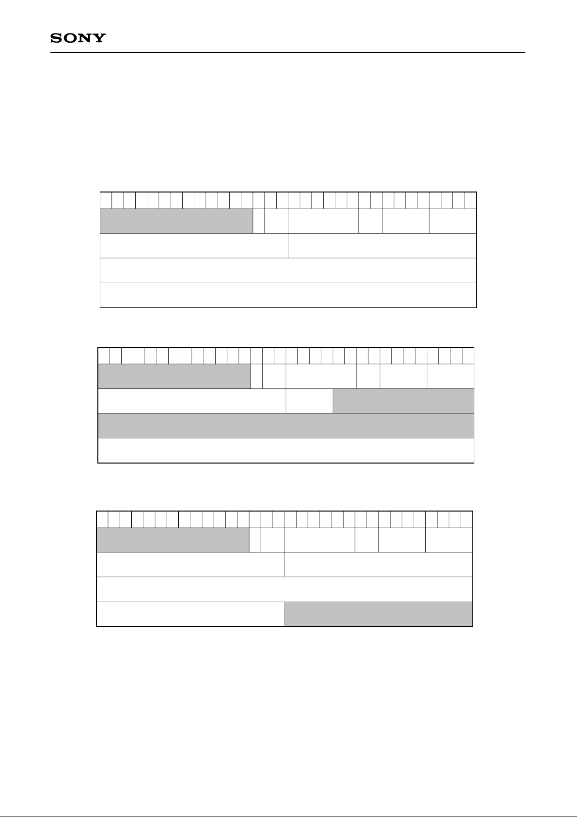
CXD1948R
6-5-1-2. Quadlet Transmit
The data format for quadlet transmit is shown below.
The 1st quadlet contains packet control information. The 2nd and 3rd quadlets contain 16-bit Destination ID
and 48-bit Destination Offset for request, or Response Code for response. The 4th quadlet is quadlet data for
Read responses and Write Quadlet requests. It is Data Length and Reserved for Block Read request.
Quadlet Write Request Transmit Format
031302928272625242322212019181716151413121110987654321
tCode priorityspd
imm
destinationOffsetLow
quadlet data
tLabel
rt
destinationOffsetHighdestinationID
Quadlet Read Response Transmit Format
destinationID
Block Read Request Transmit Format
dataLength
imm
quadlet data
imm
destinationOffsetLow
tLabel
rCode
tLabel
031302928272625242322212019181716151413121110987654321
tCode priorityspd rt
031302928272625242322212019181716151413121110987654321
tCode priorityspd
rt
destinationOffsetHighdestinationID
– 53 –
Page 54

Quadlet Transmit Fields
CXD1948R
Field Name
imm
spd
tLabel
rt
tCode
priority
destinationID
destinationOffsetHigh,
destinationOffsetLow
quadlet data
rCode
dataLength
Description
Immediately tries to transmit continuously after Acknowledge is sent, if “1” is set
(Used for Phy Read and Lock Response.)
Transmit speed
00: 100Mbps; 01: 200Mbps; 10: 400Mbps; 11: Reserved
Transaction Label. Used as a pair with response packet relative to request packet.
This packet’s Retry Code
00: New; 01: Retry-X, 10: Retry-A, 11: Retry-B
This packet’s Transaction Code
This packet’s Priority Level
For values other than “0”, the transmitter uses Priority Arbitration relative to this packet
Indicates this packet’s Destination bus number in 10 bits and the Node number in 6 bits
Two continuous such areas indicate Destination Node address space address.
This address must be in quadlet units.
Writes transmit data for Quadlet Write requests and Quadlet Read response
Response Code for Quadlet Response packet
Writes how many bytes requested for Block Read request
– 54 –
Page 55
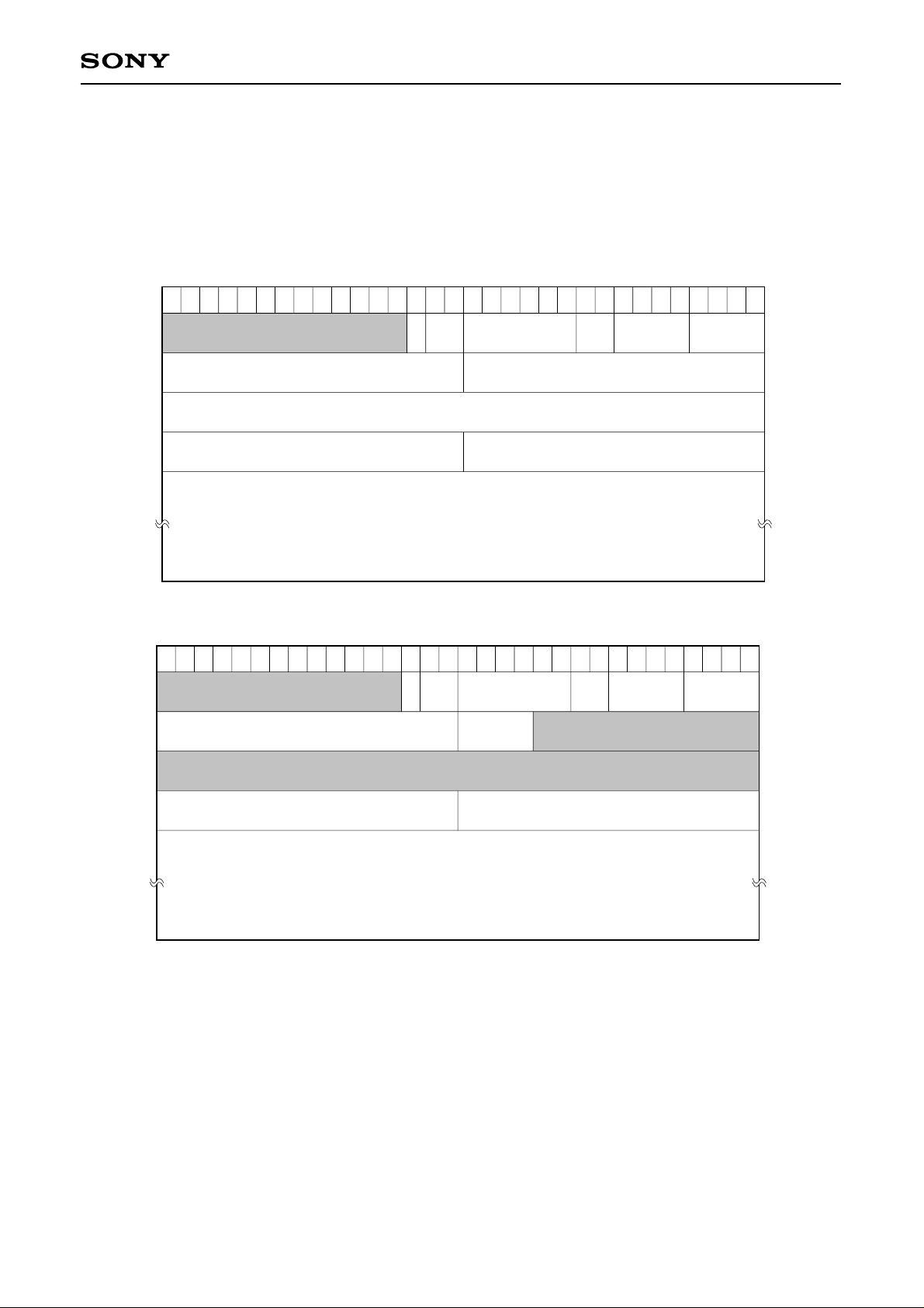
CXD1948R
6-5-1-3. Block Transmit
The data format for block transmit is shown below.
The 1st quadlet contains packet control information. The 2nd and 3rd quadlets contain 16-bit Destination ID
and 48-bit Destination Offset for request, or Response Code for response. The 4th quadlet contains data
length and Extended Transaction Code (all “0” except for Lock Transaction).
Block Transmit Format
031302928272625242322212019181716151413121110987654321
tCode priorityspd
imm
destinationOffsetLow
tLabel
rt
destinationOffsetHighdestinationID
dataLength
Block Read or Lock Transmit Format
destinationID
dataLength
black data
imm
black data
tLabel
rCode
extendedTcode
031302928272625242322212019181716151413121110987654321
tCode priorityspd rt
extendedTcode
– 55 –
Page 56
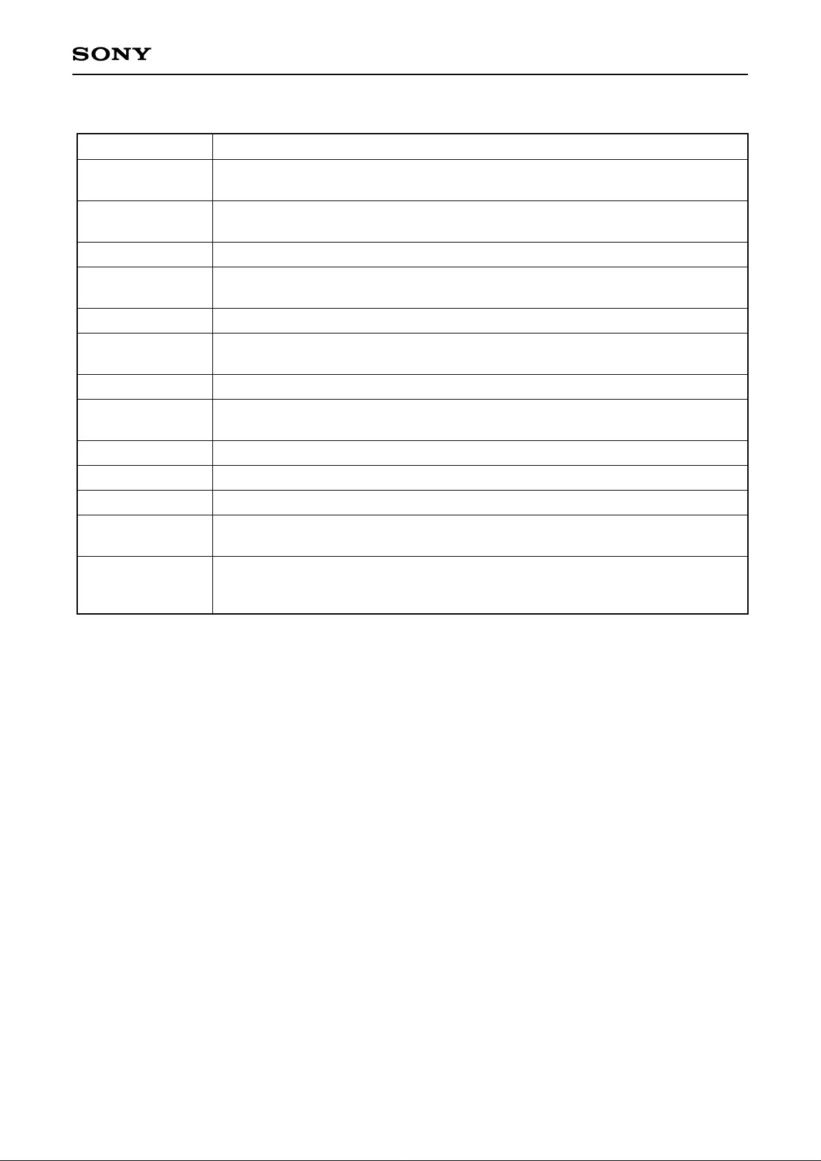
Block Transmit Fields
CXD1948R
Field Name
imm
spd
tLabel
rt
tCode
priority
destinationID
destinationOffsetHigh,
destinationOffsetLow
quadlet data
rCode
dataLength
extendedtCode
Description
Immediately tries to transmit continuously after Acknowledge is sent, if “1” is set
(Used for Phy Read and Lock Response.)
Transmit speed
00: 100Mbps; 01: 200Mbps; 10: 400Mbps; 11: Reserved
Transaction Label. Used as a pair with response packet relative to request packet.
This packet’s Retry Code.
00: New; 01: Retry-A, 10: Retry-A, 11: Retry-B
This packet’s Transaction Code.
This packet’s Priority Level.
For values other than “0”, the transmitter uses Priority Arbitration relative to this packet.
Indicates this packet’s Destination bus number in 10 bits and the Node number in 6 bits.
Two continuous such areas indicate Destination Node address space address.
This address must be in quadlet units.
Writes transmit data for Quadlet Write requests and Quadlet Read response.
Response Code for Quadlet Response packet.
Writes how many bytes requested for Block Read request.
Specifies actual Lock Action performed by this packet data when tCode is a Lock
Transaction.
block data
Writes transmitted data. This data is not written in FIFO when dataLength = “0”. The first
byte of the block must indicate the upper byte of the first data, regardless of data
Destination or Source listing.
– 56 –
Page 57
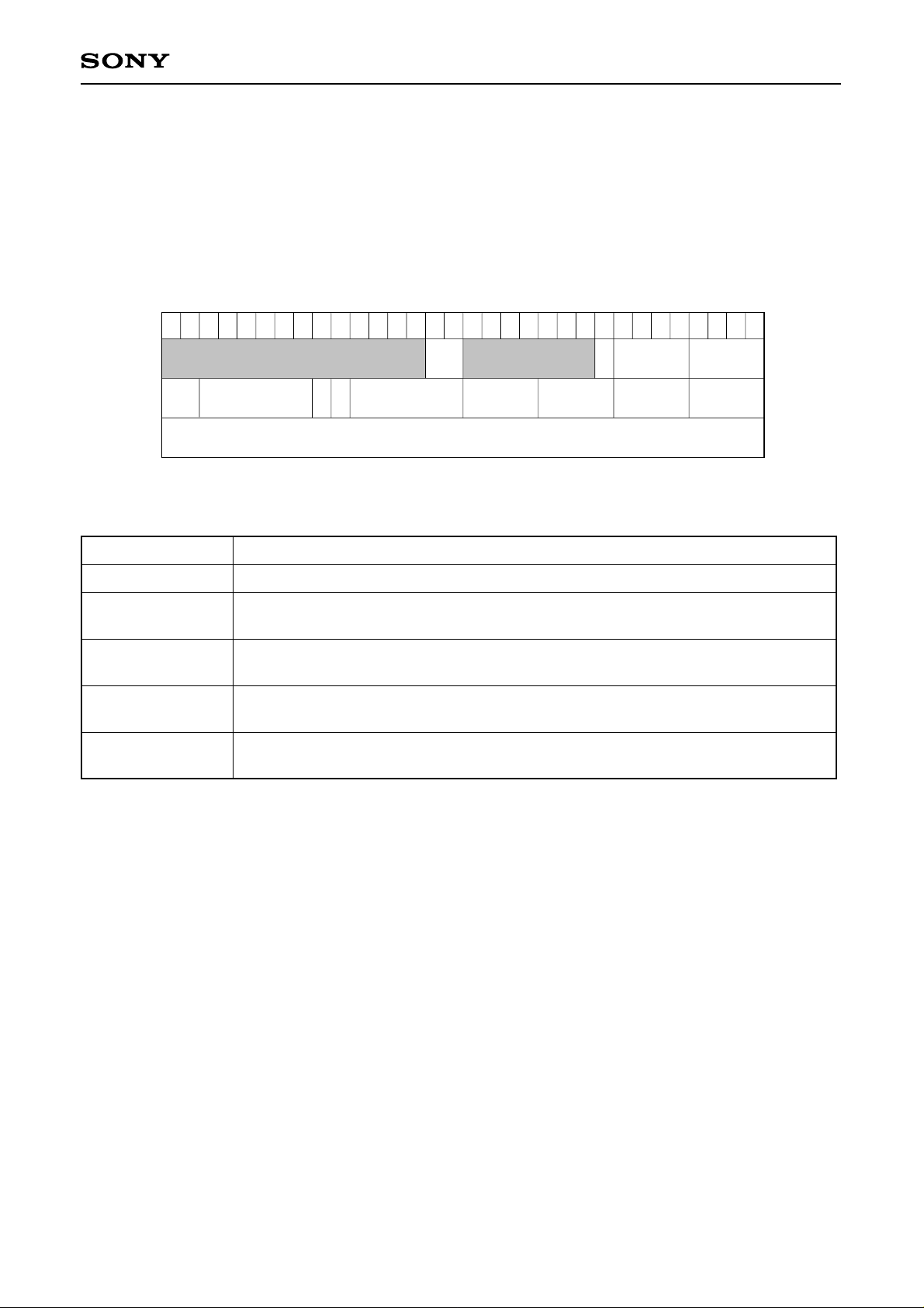
CXD1948R
6-5-1-4. Unformatted Transmit (Phy Configuration Packet)
The data format for unformatted transmit during Phy Configuration packet transmit is shown below.
The 1st quadlet contains packet control information. The remaining quadlets contain data, and get on the bus
and are transmitted regardless of format. There is no CRC attached to the packet data.
Further, there is no CRC attached to the first quadlet.
Logical-inverse is not added at Link Core, so it must be added when transmitting.
Unformatted Transmit Format 1 (PHY configuration Packet)
031302928272625242322212019181716151413121110987654321
tCode
= 1110
phy_ID 0000gap_cnt00 R T 0000 0000 0000
logical inverse of 2nd quadlet data
priorityspd 1
Unformatted Transmit (PHY Configuration Packet) Fields
Field Name
00
phy_ID
R
T
gap_cnt
Indicates that the transmit packet is a Phy configuration packet.
Sets the force_root bit of the node with this Phy_ID sets to “1”.
(Only valid when R is set at “1”.)
Sets the force_root bit of the node with this Phy_ID to “1” when set at “1”, and clears
other nodes’ force_root bit. The Phy_ID area is ignored when set at “0”.
When set to “1”, all nodes use the value of the gap_cnt field to reset their own
gap_Count values.
Indicates values of all node new Phy_CONFIGURATION.gap_Count.
This value becomes valid when it is received. (when the T field is “1”)
Description
– 57 –
Page 58

CXD1948R
6-5-1-5. Unformatted Transmit (Link-on Packet)
The data format for unformatted transmit during Link-on packet transmit is shown below.
The 1st quadlet contains packet control information. The remaining quadlets contain data, and are transmitted
regardless of format. There is no CRC attached to the packet data. Further, there is no CRC attached to the
first quadlet.
Logical-inverse is not added at Link Core, so it must be added when transmitting.
Unformatted Transmit Format 1 (Link-on Packet)
031302928272625242322212019181716151413121110987654321
tCode
= 1110
priorityspd 1
phy_ID 000001 0000 0000 0000
00000000
logical inverse of 2nd quadlet data
Unformatted Transmit (Link-on Packet) Fields
Field Name
01
phy_ID
Indicates that the transmit packet is a Link-on packet.
Indicates the Phy chip ID of this packet’s Destination.
Description
– 58 –
Page 59
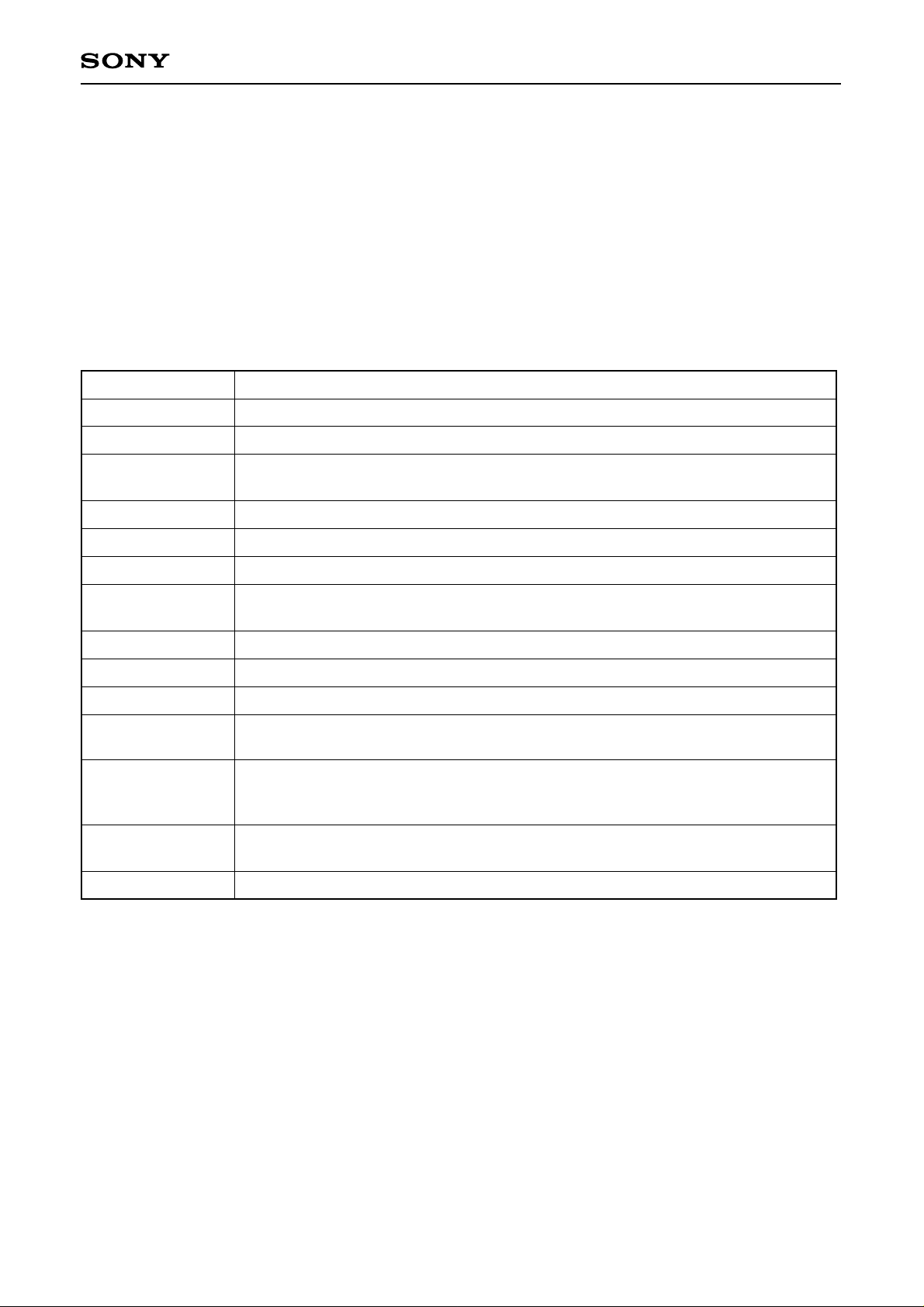
6-5-2. Asynchronous Receive (CXD1948R → Host Bus)
The following are the three basic formats for asynchronous data during receive.
a) No-data Packets (Used for quadlet read requests and all write responses.)
b) Quadlet Packets (Used for quadlet write requests, quadlet read request and block read responses.)
c) Block Packets (Used for lock requests, lock responses, block write requests and block read responses.)
The names of receive data areas and their contents are given below.
Async Receive Fields
CXD1948R
Field Name
destinationID
tLabel
rt
tCode
priority
sourceID
destinationOffsetHigh,
destinationOffsetLow
rCode
quadlet data
dataLength
extendedtCode
block data
Description
This node’s bus number (all “0” if “local bus”) and node number (all “1” if broadcast)
Transaction Label. Used as a pair with response packet relative to request packet.
This packet’s Retry Code.
00: New; 01: Retry-X, 10: Retry-A, 11: Retry-B
This packet’s Transaction Code
This packet’s Priority Level
The Node ID of the node that sent this packet
Two continuous such areas indicate Destination Node address space address.
This address must be in quadlet units.
Response Code for Response packet
Received data is written for quadlet write requests and quadlet read response.
The number of bytes in received block type’s packet data.
Specifies actual Lock Action performed by this packet data when tCode is a Lock
Transaction.
Received data is written. This data is not written in FIFO when dataLength = “0”. The
first byte of the block must indicate the upper byte of the first data, regardless of data
destination or Source listing.
spd
ackSent
Speed of received packet.
00: 100Mbps; 01: 200Mbps; 10: 400Mbps; 11: Reserved
Acknowledge code sent by Link Core relative to this packet is written.
– 59 –
Page 60
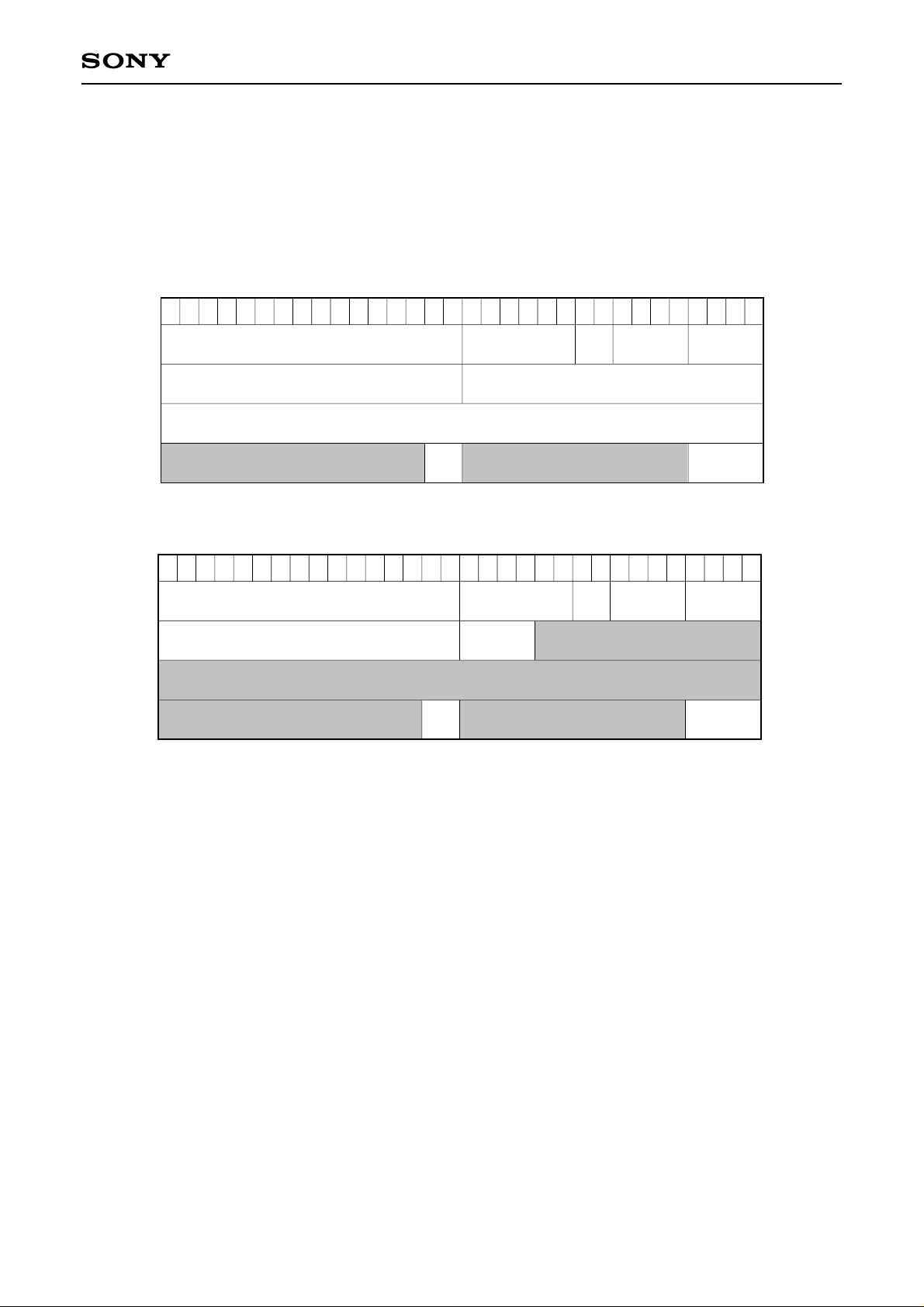
CXD1948R
6-5-2-1. No-data Receive
The data format for no-data receive is shown below.
The 1st quadlet contains the destination ID and other packet headers. The 2nd and 3rd quadlets contain 16-bit
source ID, and 48-bit destination offset for request and the Response Code for response. The last quadlet
contains packet receive status.
Quadlet Read Request Receive Format
031302928272625242322212019181716151413121110987654321
destinationID
sourceID destinationOffsetHigh
Write Response Receive Format
destinationID
sourceID rCode
tLabel
destinationOffsetLow
spd acksent
tLabel
spd acksent
tCode priorityrt
tCode priorityrt
031302928272625242322212019181716151413121110987654321
– 60 –
Page 61
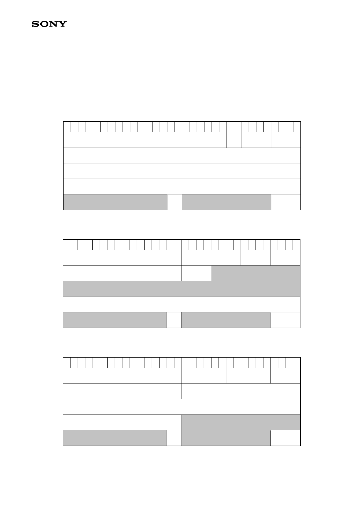
CXD1948R
6-5-2-2. Quadlet Receive
The format for Quadlet Receive is shown below.
The 1st quadlet contains the destination ID and other packet headers. The 2nd and 3rd quadlets contain 16-bit
source ID, and 48-bit destination offset for request and the Response Code for response. The 4th quadlet
contains data for Read request and Write Quadlet request, and data length and Reserved for Block Read
request. The last quadlet contains packet receive status.
Quadlet Write Request Receive Format
031302928272625242322212019181716151413121110987654321
destinationID
sourceID destinationOffsetHigh
Quadlet Read Response Receive Format
destinationID
sourceID rCode
tLabel
destinationOffsetLow
quadlet data
spd acksent
tLabel
quadlet data
tCode priorityrt
tCode priorityrt
031302928272625242322212019181716151413121110987654321
Block Read Request Receive Format
destinationID
sourceID destinationOffsetHigh
dataLength
spd acksent
tLabel
destinationOffsetLow
spd acksent
tCode priorityrt
– 61 –
031302928272625242322212019181716151413121110987654321
Page 62
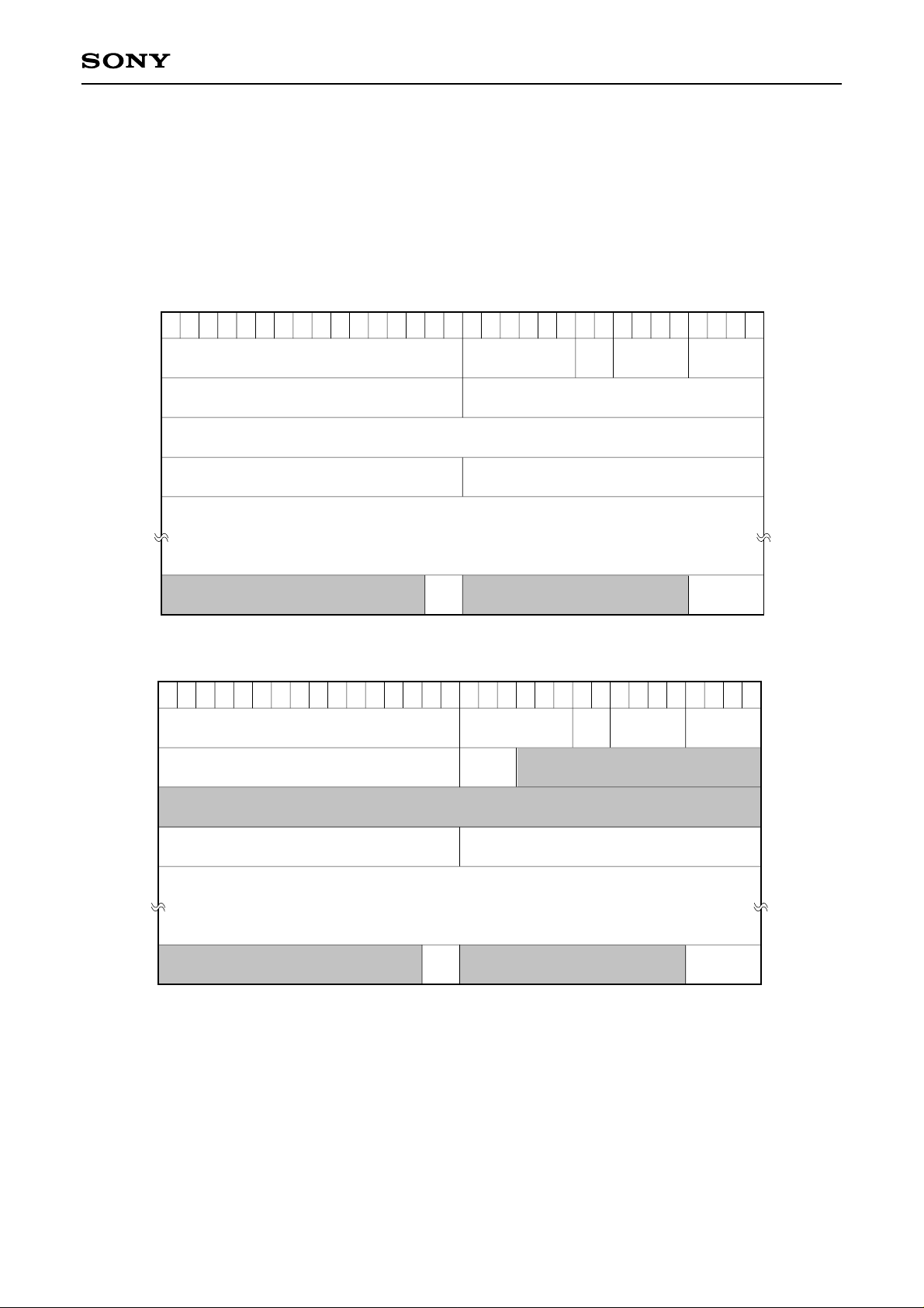
CXD1948R
6-5-2-3. Block Receive
The format for Block Receive is shown below.
The 1st quadlet contains the destination ID and other packet headers. The 2nd and 3rd quadlets contain 16-bit
source ID, and 48-bit destination offset for request and the Response Code for response. The 4th quadlet
contains data length and Extended Transaction Code (all “0” except for Lock Transaction). This is followed by
Block data. The last quadlet contains packet receive status.
Block Receive Format
031302928272625242322212019181716151413121110987654321
destinationID
sourceID destinationOffsetHigh
destinationOffsetLow
dataLength
Block Read or Lock Response Receive Format
destinationID
sourceID
tLabel
extendedtCode
block data
spd acksent
tLabel
rCode
tCode priorityrt
tCode priorityrt
031302928272625242322212019181716151413121110987654321
dataLength
block data
spd acksent
extendedtCode
6-6. Self-ID Packet Receiving Error Processing
In the Self-ID phase after bus reset on the CXD1948R, if the Self-ID packet could not be received correctly,
Self-ID packet receive is stopped immediately and the Node_sum value becomes “0”.
The external microcomputer thus can judge that the Self-ID phase could not be completed correctly.
– 62 –
Page 63
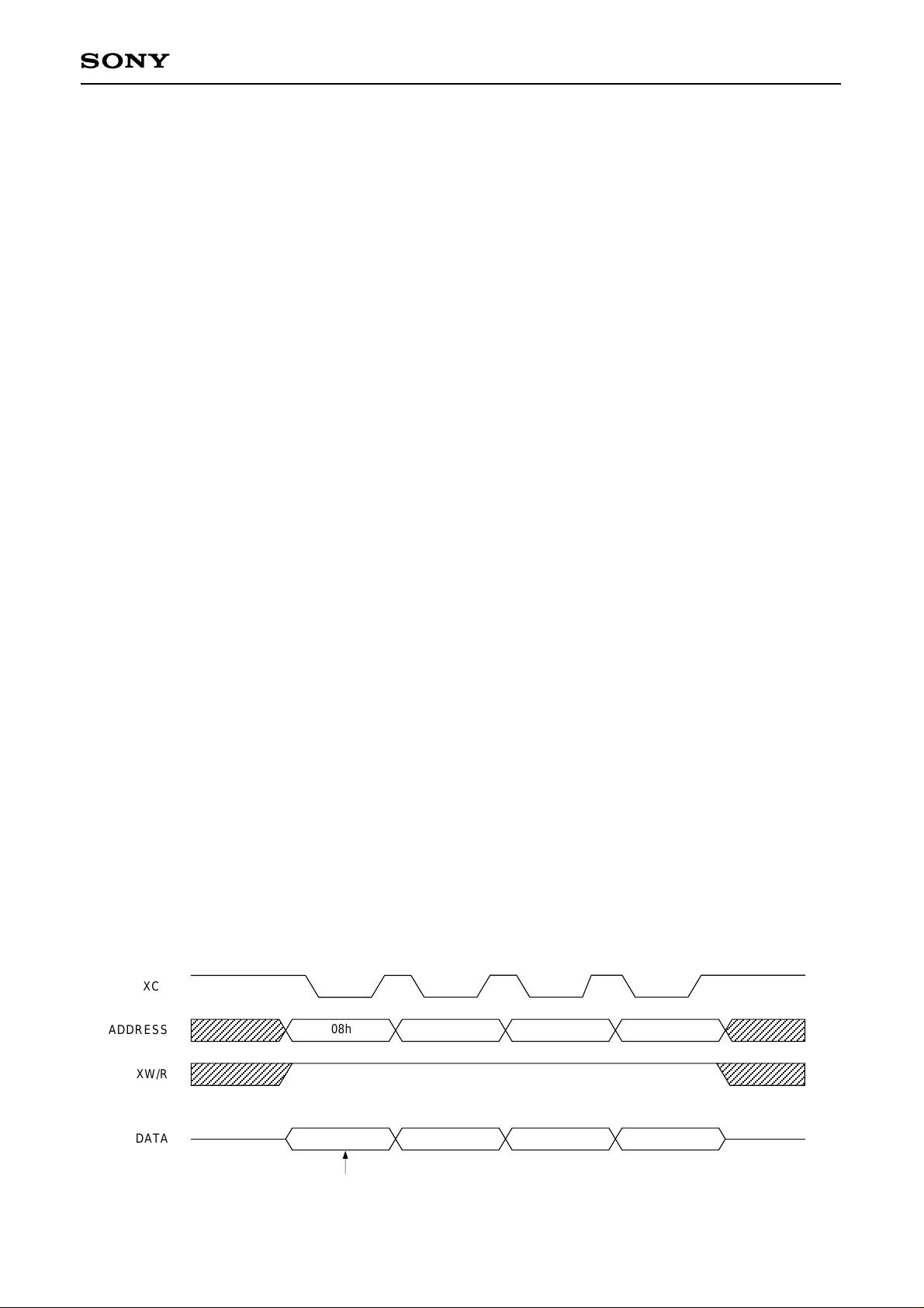
CXD1948R
7. Insert Packet
7-1. Insert Packet Transmission
The CXD1948R has a function where the data set by the host I/F is inserted as isochronous packet and it is
transmitted when the transport stream data is being isochronous-transmitted.
The transmit method is the same as for asynchronous packet transmit; it is done by accessing the specified
CFR (refer to CFR Address Map) address (64 to 6C).
• Insert Packet Transmit
The external writes packet data in the CXD1948R internal IPF in order to perform insert packet transmit. At
this time only the first quadlet of the packet is written in the CFR IPBWrite (first quadlet of the packet)
register (64h). The second through the next to the last quadlets are written in the CFR IPBWrite register
(68h).
Then the last quadlet is written in the IPBWrite (confirm write) register (6Ch) to store the packet in IPB.
There are two types of Insert packet transmission, as described below.
(1) Transmission by writing the last quadlet in IPBWrite (confirm write).
(2) Transmission by setting the CFR IPTxGo register to high.
If IPTxGo is used, the data written earlier in IPB can be transmitted as is, with no changes. The IPTxGo
register only becomes “0” when Insert packet transmit is actually performed, or if it is erased from IPB due to
transmit Late processing or the like.
The time stamp added to the Insert packet takes the fall timing of the Packet Gap input directly after IPTxGo
register value changes from “0” to “1”.
Once the time stamp is added, processing is the same as for transport stream data.
The FIFO capacity for the Insert packet is 188 bytes. Data which exceeds this capacity can not be transmitted.
In this case, the data up to 188 bytes is valid.
If the transmitted data is less than 188 bytes, all data bits other than those written are set to “1” and
transmitted.
The written data is held after transmit, and to continue sending a packet with the same contents, it is only
necessary to set the IPTxGo register to “1” after confirming that it changed to “0”.
Writing to IPB must be done in quadlet units.
The procedure for transmitting a 4 quadlet Insert packet is described below.
(for 8 bit interface)
(1) Confirming that transmit of the previously written packet is complete
The CFR Control register (08h to 0bh) is read to confirm that its first bit (IPTxGo bit) is low. If it is high, it
means that transmit of the previously written packet has not been performed.
XCS
ADDRESS
XW/R
08h
09h 0Ah 0Bh
DATA
xxxxxx1xb
This indicates that the Insert packet has not been transmitted.
It is “xxxxxx0xB” when an Insert packet can be written.
– 63 –
Page 64
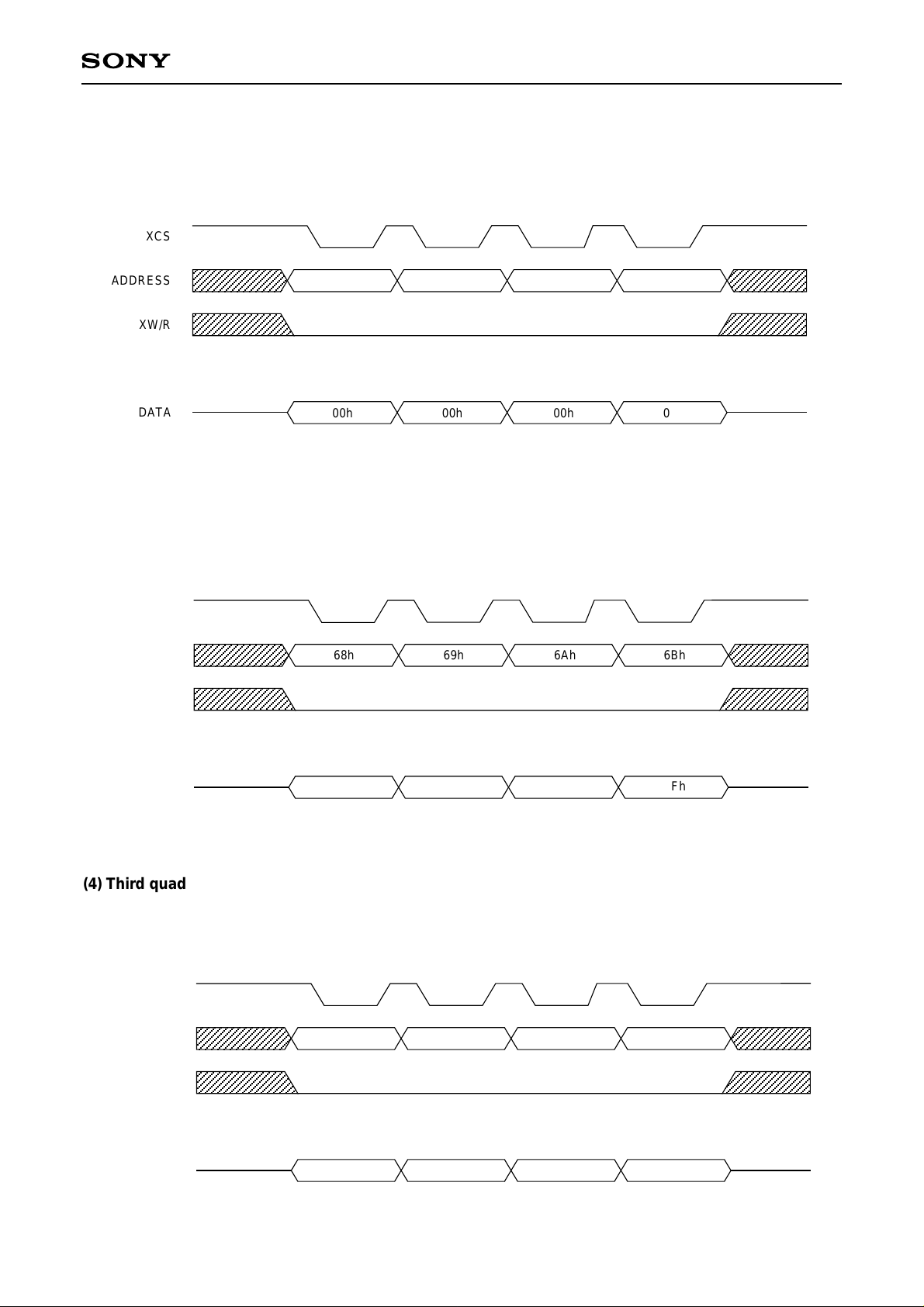
(2) First quadlet of the transmitted packet Write
Let the first quadlet of the quadlet write request packet be “00000000h”.
This is written in the CFR IPBWrite (first quadlet of the packet) register.
XCS
CXD1948R
ADDRESS
XW/R
DATA
64h 65h 66h 67h
00h 00h 00h 00h
(3) Second quadlet of the transmitted packet Write
Let the second quadlet of the quadlet write request packet be “FFC1FFFFh”.
This is written in the CFR IPBWrite register.
XCS
ADDRESS
XW/R
68h 69h 6Ah 6Bh
DATA
FFh FFh C1h FFh
(4) Third quadlet of the transmitted packet Write
Let the third quadlet of the quadlet write request packet be “F000000Ch”.
This is written in the CFR IPBWrite register.
XCS
ADDRESS
XW/R
DATA
68h 69h 6Ah 6Bh
0Ch 00h 00h F0h
– 64 –
Page 65
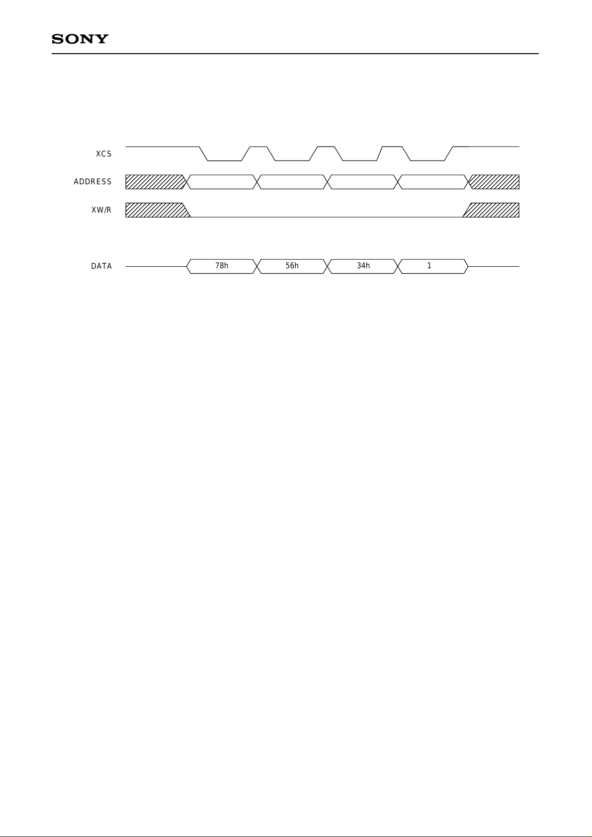
(5) Last quadlet of the transmitted packet Write
Let the last quadlet of the quadlet write request packet be “12345678h”.
This is written in the CFR IPBWrite (confirm write) register.
XCS
CXD1948R
ADDRESS
XW/R
DATA
6Ch 6Dh 6Eh 6Fh
78h 56h 34h 12h
The 4-quadlet data is stored in the IPB as shown above. The CXD1948R transmits the packet with 1394
header and CIP header automatically attached, as with the case for the normal transport stream data, after the
time stamp is added to the packet stored in the IPB. If Insert packet transmit does not take place due to Late
processing, the CFR interrupt register (0Ch to 0Fh) must be read to confirm that the IpktLate bit is high.
Set the CFR IPTxGo register to high to add the time stamp when transmitting the Insert packet data again
without updating its contents.
– 65 –
Page 66
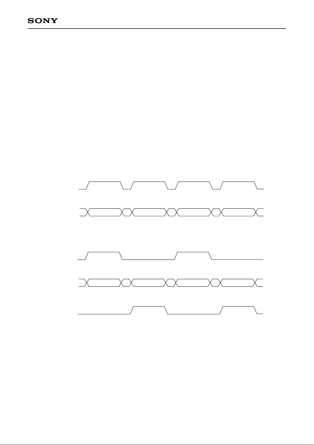
CXD1948R
7-2. Adding a Time Stamp to the Insert Packet
A time stamp must be added to the Insert packet in order to process it as an isochronous packet.
The CXD1948R adds the time stamp using PACKETGAP input.
Concretely, the TxDelay register value added at the falling edge of the PACKETGAP input immediately after
the Insert packet has been written to the IPB becomes the time stamp value of the Insert packet to be
transmitted.
The time stamp must be added to the Insert packet during the interval when there is no transport stream data
input.
When transmitting the entire transport stream, there is no gap during which to input PACKETGAP, so the
Insert packet cannot be transmitted.
When transmitting the Insert packet, be sure to select a program from the transport stream and then perform
transmission.
At this time, PACKETGAP input can add the time stamp to the Insert packet by inputting the PACKETEN of the
non-selected programs as is.
When transmitting the entire transport stream
PACKETEN
AIDT
Program 1 Program 2 Program 1 Program 3
When transmitting only program 1 within the transport stream
PACKETEN
AIDT
PACKETGAP
Program 1 Program 2 Program 1 Program 3
– 66 –
Page 67
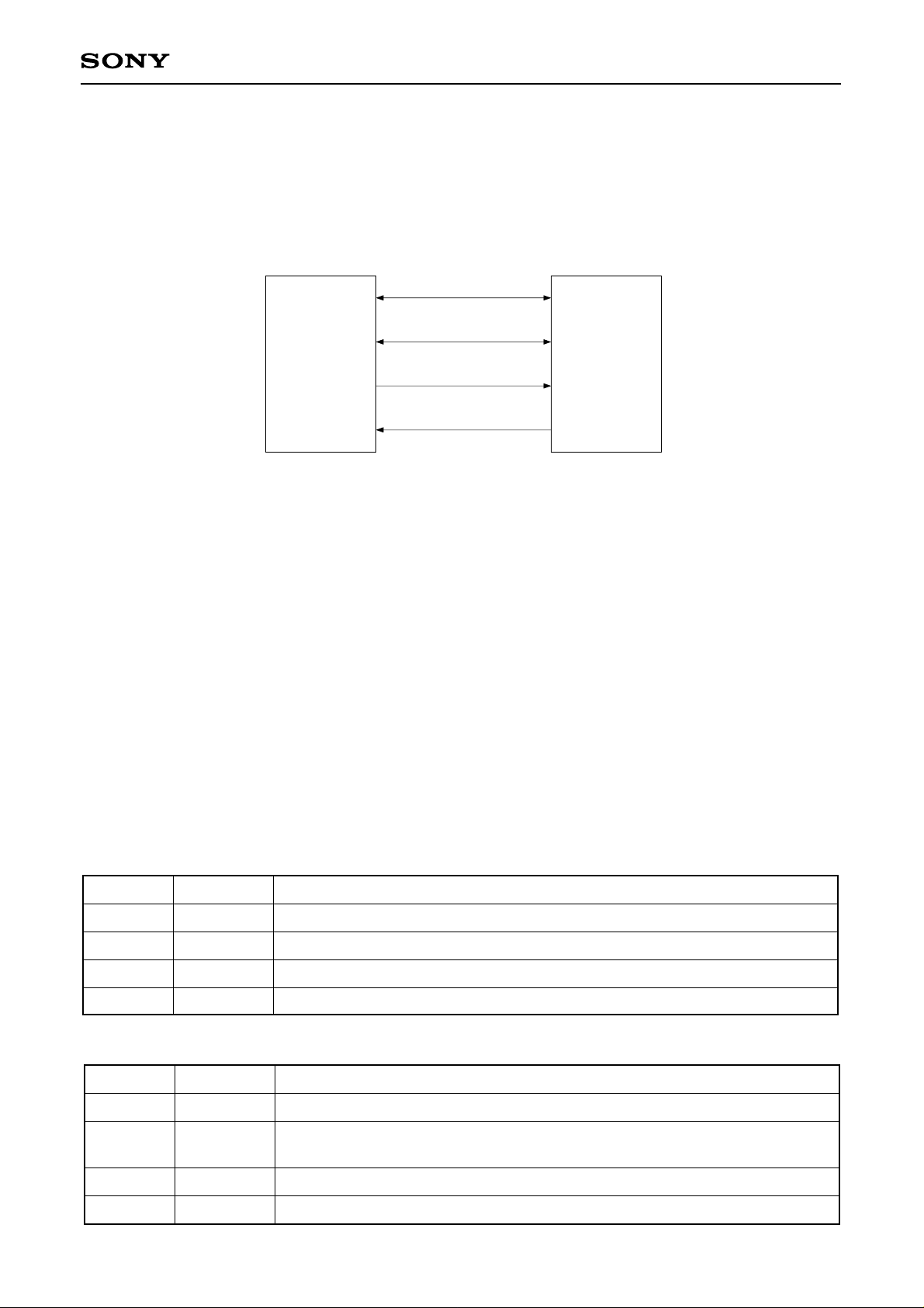
CXD1948R
8. Link-Phy Communication
8-1. Link-Phy Interface Specifications
The CXD1948R and Phy layer chip communicate using the four signals shown in the block diagram below:
D [0 : 3], CTL [0 : 1], LREQ and SYSCLK.
D [0 : 3]
CTL [0 : 1]
1394
Link Layer
CXD1948R
LREQ
SYSCLK
1394
Phy Layer
The roles of the signals are as follows.
D [0 : 3] in/out Bidirectional data line
CTL [0 : 1] in/out Bidirectional control line
LREQ out LREQ out Request signal line from CXD1948R to Phy chip.
Used for bus access and Phy register read/write requests.
SYSCLK in System clock (49.152MHz) supplied from Phy to the CXD1948R.
The types of communication and their contents are described below.
8-2. Communication
There are four types of communication between Phy Link: Request, Status, Transmit and Receive. Except for
request, all commands are initialized by the Phy chip.
8-2-1. Bus controlling
CTL [0 : 1] controls communication between Phy and the CXD1948R. The communication contents differ
depending on if Phy or the CXD1948R is controlling.
a) Phy controlling
CTL [0 : 1] Name
00
01
10
11
Idle
Status
Receive
Transmit
Bus is idle (Default mode)
Phy is sending status information to the CXD1948R
Phy is sending a packet to the CXD1948R
The CXD1948R authorized packet transmit
Description of Activity
b) CXD1948R controlling
CTL [0 : 1] Name
00
Idle
The CXD1948R completed transmit
Description of Activity
01
10
11
Hold
Transmit
Reserved
The CXD1948R is holding the bus until transmit preparations are complete. Or,
the CXD1948R is trying to transmit another packet without arbitration.
The CXD1948R is transmitting a packet to Phy
Not used
– 67 –
Page 68
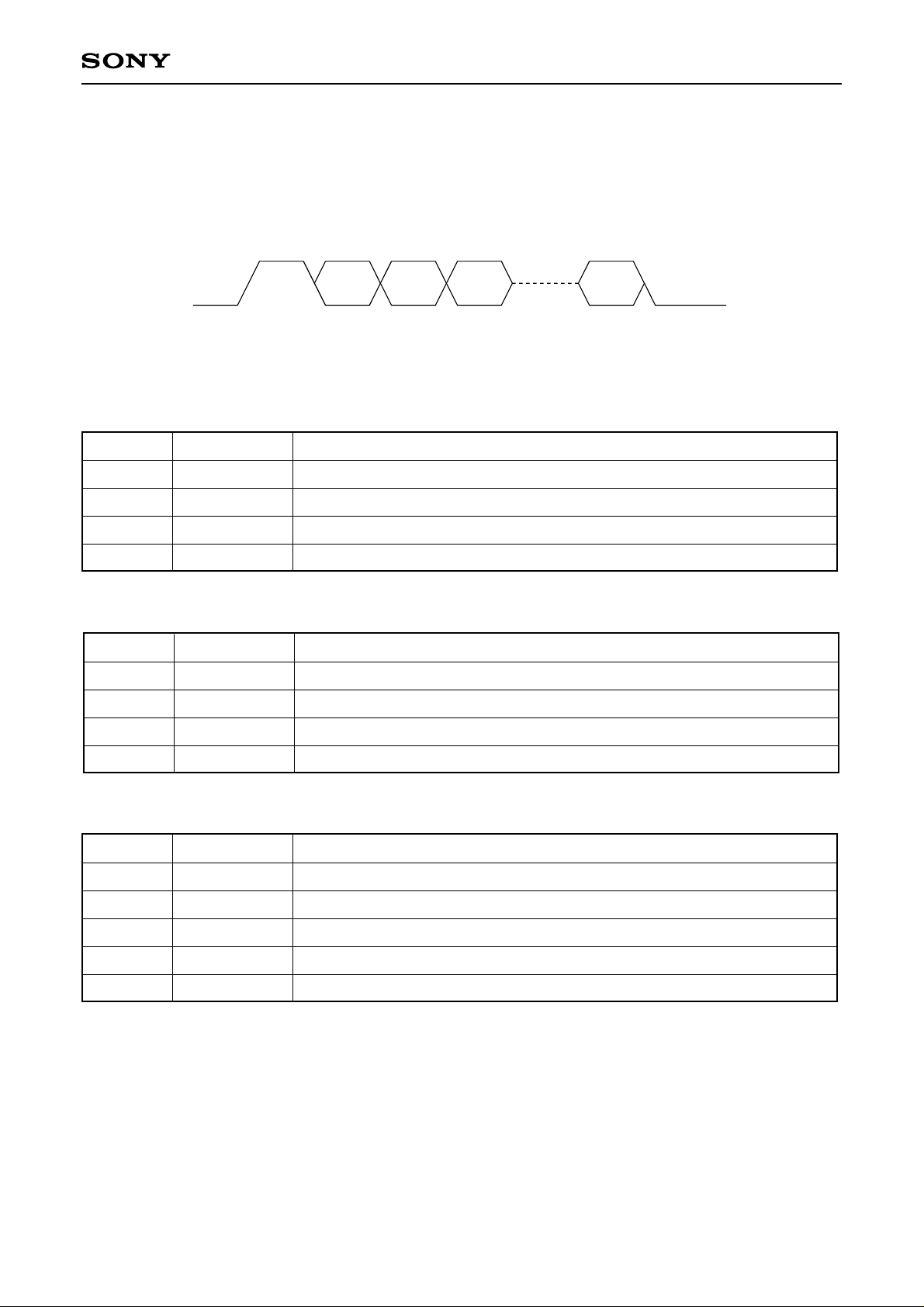
CXD1948R
8-2-2. Request
The CXD1948R always uses serial communication of LREQ to send a request to Phy when a request to the
bus or access to the Phy register is required.
There are three types of request: Bus Request, Read Register Request and Write Register Request. The
timing chart and contents are illustrated below.
LR3LR2LR1LR0 LR (n – 2) LR (n – 1)
a) Bus Request (length of stream: 7 bits)
Bit Name
0
1 to 3
4 to 5
6
Start Bit
Request Type
Request Speed
Stop Bit
Transmit start bit. Always “1”.
Indicates type of request. (Refer to Request Type table.)
Indicates request communication speed. (Refer to Request Speed table.)
Last transmit bit. Always “0”.
b) Read Register Request (length of stream: 9 bits)
Bit Name
0
1 to 3
4 to 7
8
Start Bit
Request Type
Address
Stop Bit
Transmit start bit. Always “1”.
Indicates type of request. (Refer to Request Type table.)
Address for Phy register read.
Last transmit bit. Always “0”.
c) Write Register Request (length of stream: 17 bits)
Bit Name
0
1 to 3
4 to 7
8 to 15
Start Bit
Request Type
Address
Data
Transmit start bit. Always “1”.
Indicates type of request. (Refer to Request Type table.)
Address for Phy register write.
Write data for Phy register specified by Address.
Description
Description
Description
16
Stop Bit
Last transmit bit. Always “0”.
– 68 –
Page 69
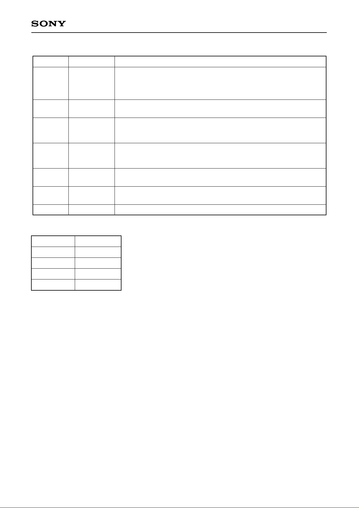
Request Type
CXD1948R
LREQ [1 : 3]
000
001
010
011
100
101
110, 111
Request Speed
Name
ImmReq
IsoReq
PriReq
FairReq
RdReq
WrReq
Reserved
Description
Immediate bus acquisition request.
To output Ack for an asynchronous packet reception, immediate bus
acquisition is requested without arbitration when Idle is detected.
Used to transmit Acknowledge.
Isochronous request. Requests execution of arbitration.
Used for isochronous transmit.
Priority request.
Requests arbitration after Subaction Gap, ignoring Fair protocol.
Used for Cycle Master request.
Fair request
Requests execution of arbitration after subaction gap according to fair protocol.
Used for Fair transmit.
Read request.
Requests return of register contents according to Status Transfer.
Write request.
Requests write to specified address.
Reserved.
LREQ [4 : 5] Data Rate
00
01
10
11
100Mb/s
200Mb/s
400Mb/s
Reserved
8-2-2-1. Bus Request
In order to access Fair or Priority, waits at least 1 clock after the CXD1948R becomes idle to send the request.
When the CTL pin is in receive state (CTL [0 : 1] = 10), CXD1948R interprets the request as being refused. It
is reissued 1 clock after the next idle state.
In the Cycle Master node, the cycle start message is sent using Priority Request. In order to request sending
of isochronous data, the CXD1948R can issue an isochronous request after receiving cycle start. Phy clears
the isochronous request only after the bus is acquired successfully.
The CXD1948R must issue ImmReq while it is receiving a packet addressed to itself in order to send
Acknowledge. When packet reception is completed, Phy immediately acquires the bus and gives authorization
to the CXD1948R. If the header CRC is not erroneous, the CXD1948R returns an Acknowledge signal.
However, if the header CRC is erroneous, the CXD1948R immediately releases the bus. The CXD1948R can
not use this authorization to send other packets. In order to ensure this operation, the CXD1948R waits 160ns
after the completion of packet reception. Then Phy acquires the bus once again, and a CRC error
Acknowledge is sent. Then it releases the bus and continues with another request.
– 69 –
Page 70
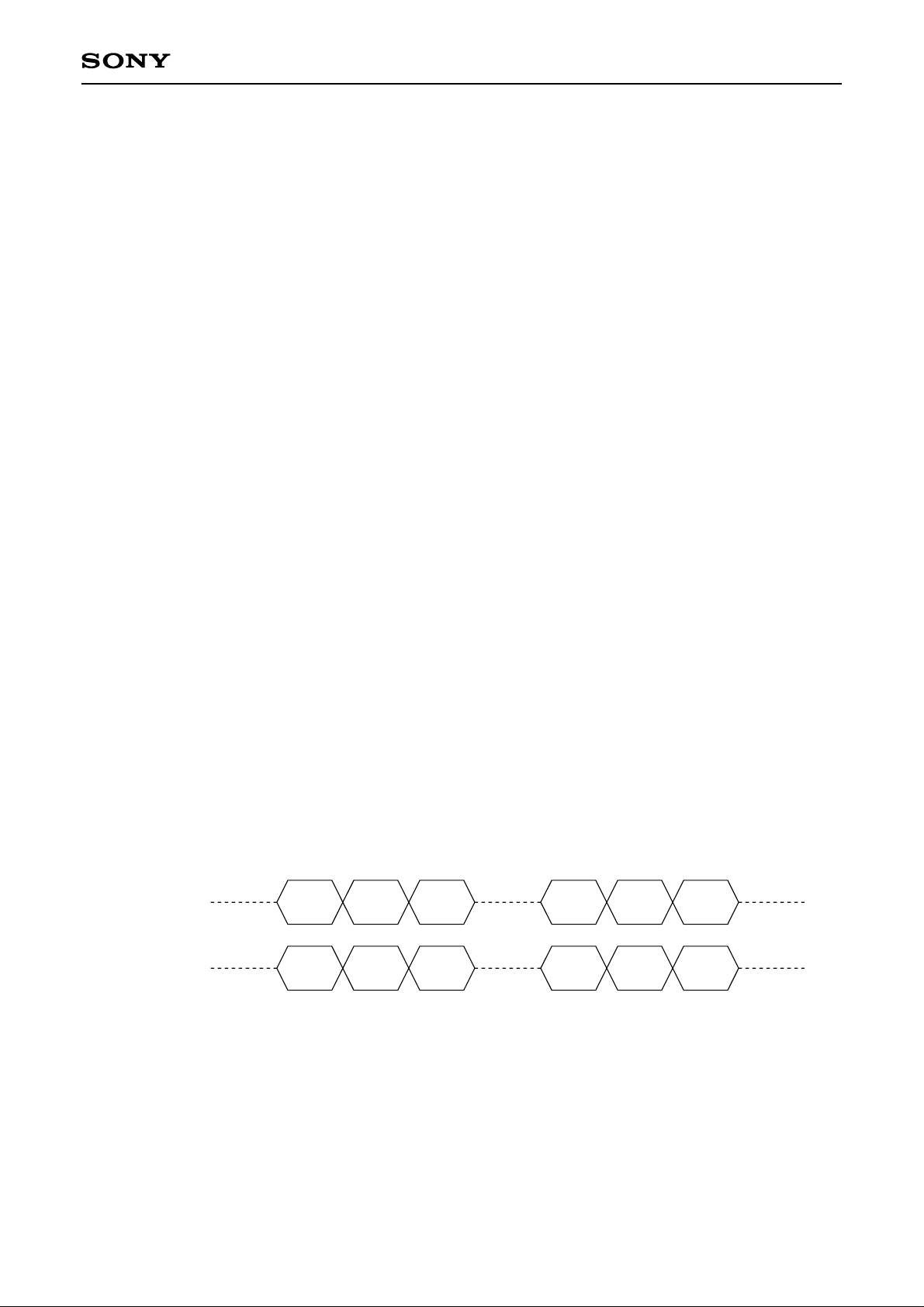
CXD1948R
Consider a case in which two different nodes confirm that the packet sent is addressed to them (one is correct,
one is wrong), and both nodes issue an ImmReq before CRC check. The Phy of both nodes try to capture the
bus immediately after packet receive is completed.
At this time, there will be a momentary collision on the local bus. This can be detected by all of the Phy
connected to the bus. This collision is not interpreted as Bus Reset, but as high impedance state. After CRC
check is completed, the wrong node will withdraw its request and the high impedance state is discontinued.
The expected Acknowledge is lost as a side effect of this, but is processed by the host protocol.
8-2-2-2. Read/Write Request
When the CXD1948R requests reading of a specific register’s contents, Phy transmits the register contents to
the CXD1948R by Status Transfer. Even if packets are received while Phy is sending status information to the
CXD1948R, Phy continues processing until the register contents are transferred.
For a Write Request, Phy loads the data fields into the appropriate register as soon as transmission is
completed. The CXD1948R can read/write at any time.
8-2-3. Status
Status transmission is started by Phy when it has some data to transmit to the CXD1948R. Phy begins
transmission by simultaneously setting CTL [0 : 1] to “01b” and the first 2 bits of Status information to D [0: 1].
Phy maintains CTL = Status during status transmission.
Phy may finish Status transmission early by setting the CTL value to some other value. This happens if a
packet arrives before Status transmit is completed. When such an interruption occurs, Phy repeatedly tries
resending until the transfer is successful.
There must be at least one idle cycle in a continuous Status transmission.
Phy normally sends the first four bits of Status to the CXD1948R. These bits are the Status Flags required for
the CXD1948R state machine. When transmission of a request containing a Read Request is completed, or
when Phy has information to send to the CXD1948R or the transaction layer, Phy sends the first Status packet
to the CXD1948R.
The only state in which Phy sends register contents automatically to the CXD1948R is that after completion of
Self-Identification, and Physical_ID register contents containing a new node address are transmitted. The
transmit timing and bit definitions are illustrated below.
– 70 –
01010100 00 00PHY Ctl [0 : 1]
S [14, 15]S [2, 3]S [0, 1]00 00 00PHY D [0 : 1]
Page 71
Status bit (Length of stream: 16 bits)
CXD1948R
Bit Name
0
1
2
3
Arbitration
Reset Gap
Subaction Gap
Bus Reset
State Time-out
Indicates detection of idle state, for Bus Arbitration Reset Gap Time.
This bit is used by the CXD1948R busy/retry state machine.
Indicates detection of idle state, for Subaction Gap Time.
This bit is used by the CXD1948R to detect the end of the isochronous cycle.
Indicates Phy in bus reset state.
Indicates that Phy state machine is stopped in a certain state for a long time.
Normally used for cable topology loop detection.
Description
Holds the address of the register being read when Phy is trying to send
4 to 7
Address
register contents to CXD1948R; for example, when responding to Read via
the LREQ pin.
8 to 15
Data
Holds the register being sent to CXD1948R.
8-2-4. Transmit
When the CXD1948R requests bus access via the LREQ pin, Phy performs arbitration for bus access. When
Phy wins the arbitration, Transmit is sent to the CTL pin for at least 1 SYSCLK cycle, and Idle is then asserted
for 1 cycle to give the CXD1948R the bus. After detecting transmit state from Phy, the CXD1948R asserts
either Hold or Transmit to the CTL pins to take over interface control. The CXD1948R asserts Hold until the
data is ready, in order to keep bus initiative. During this time, Phy asserts Data-on state to the bus. When the
packet is ready to transmit , the CXD1948R transmits the first bit of the packet, and at the same time asserts
Transmit to the CTL pins. After sending the last bit of the packet, the CXD1948R asserts either Idle or Hold to
the CTL pins for 1 cycle. Then it asserts Idle for 1 cycle before these pins become high impedance.
Here, when it is necessary for the CXD1948R to send another packet without releasing the bus, it indicates
Hold to Pht. In response to this, Phy asserts Transmit in the same way as before after waiting for the
minimum required time. This function is used when multiple isochronous packets are sent in succession to
different channels without the CXD1948R releasing the bus, and when a Response packet is sent following
Acknowledge. When in this way multiple transmissions are performed in succession, all transmissions are at
the same speed. This is because the speed is set at the time of arbitration to acquire the bus, and in
successive transmissions intermediate arbitrations are skipped.
As described above, when the CXD1948R completes sending the last packet on the newest bus initiative, it
releases the bus by asserting Idle to the CTL pins for 2 Sclk. When Phy detects Idle from the CXD1948R, it
starts to assert Idle to CTL for 1 clock.
– 71 –
Page 72
The timing chart for transmit is shown below.
Single Packet
CXD1948R
PHY Ctl [0 : 1] 11 00 ZZ ZZ ZZ ZZ ZZ ZZ ZZ ZZ 00
Continued Packet
PHY Ctl [0 : 1] ZZ ZZ ZZ 00 11 00 ZZ00 ZZ ZZ ZZ
CXD1948R Ctl [0 : 1]
00
00PHY D [0 : 3] 00 00 ZZ ZZ ZZ ZZ ZZ ZZ ZZ ZZ 00
ZZCXD1948R Ctl [0 : 1] ZZ ZZ 01 01 10 10 10 10 00 00 ZZ
ZZCXD1948R D [0 : 3] ZZ ZZ 00 00 D0 D1 D2 Dn 00 00 ZZ
ZZ
ZZPHY D [0 : 3] ZZ ZZ ZZ 00 00 00 ZZ00 ZZ ZZ ZZ
10
10 01 00 ZZ ZZ ZZ 01ZZ 01 10 10
Dn–1CXD1948R D [0 : 3] Dn 00 00 ZZ ZZ
ZZ: High-impedance state, D0 to Dn: packet data
ZZ 00ZZ 00 D0 D1
– 72 –
Page 73
CXD1948R
8-2-5. Receive
When data from the bus is received at Phy, it is sent from Phy to the CXD1948R in the following order.
Phy asserts Receive to the CTL pins and “all1” to the D pin. Phy indicates the start of the packet by placing a
speed code on the D pin. Next it indicates the contents of the packet, and until transmission of the last symbol
in the packet is completed, it holds the CTL pins at Receive. Phy indicates the end of the packet by asserting
Idle to the CTL pins. The speed code is specified by Phy-Link protocol, and does not include CRC calculation
or other data protect.
Phy can identify if there is data on the bus or not without looking at the packet. This also applies if a packet is
being sent at a faster speed than Phy can receive. In this case, the packet is completed by asserting Idle when
the Data-on state is completed.
If Phy supports a faster transmission speed than the CXD1948R, the CXD1948R detects the speed code and
ignores the packet until it becomes Idle again.
The timing chart for reception is illustrated below.
PHY Ctl [0 : 1]
(binary)
PHY D [0 : 3]
(hex)
00
10 10 10 10 10 10 00 00
00 F
F SP D0 D1 Dn 00 00
Note: SP means Speed Code.
Speed codes for receive
D [0 : 3] Data Rate
00xx
0100
100Mbit/s
200Mbit/s
Note 1: “xx” means that “0” was transmitted, but it is ignored for receive.
Note 2: This LSI supports 100Mbit/s and 200Mbit/s communications.
– 73 –
Page 74
CXD1948R
9. Parallel Input/Output Port
The CXD1948R has a 5-bit I/O port.
The direction of each port and the value during output mode can be set and the value during input mode can
be read by accessing the CFR using the host interface.
The status after initializing the CXD1948R is input mode for all ports.
Symbol
Pin No.
Direction switching Value setting (output)/value reading (input)
CFR register name
PORT0
PORT1
PORT2
PORT3
PORT4
44
45
46
69
70
PDIR0
PDIR1
PDIR2
PDIR3
PDIR4
PDATA0
PDATA1
PDATA2
PDATA3
PDATA4
Ports are set to output mode when the corresponding PDIR register is “1”, and to input mode when “0”.
Concretely, when PDIR0 is set to “1”, the value set in the PDATA0 register is output from the PORT0 pin.
If PDIR0 is set to “0”, the value input to the PORT0 pin is loaded to the PDATA0 register.
Each I/O port can be set independently.
– 74 –
Page 75
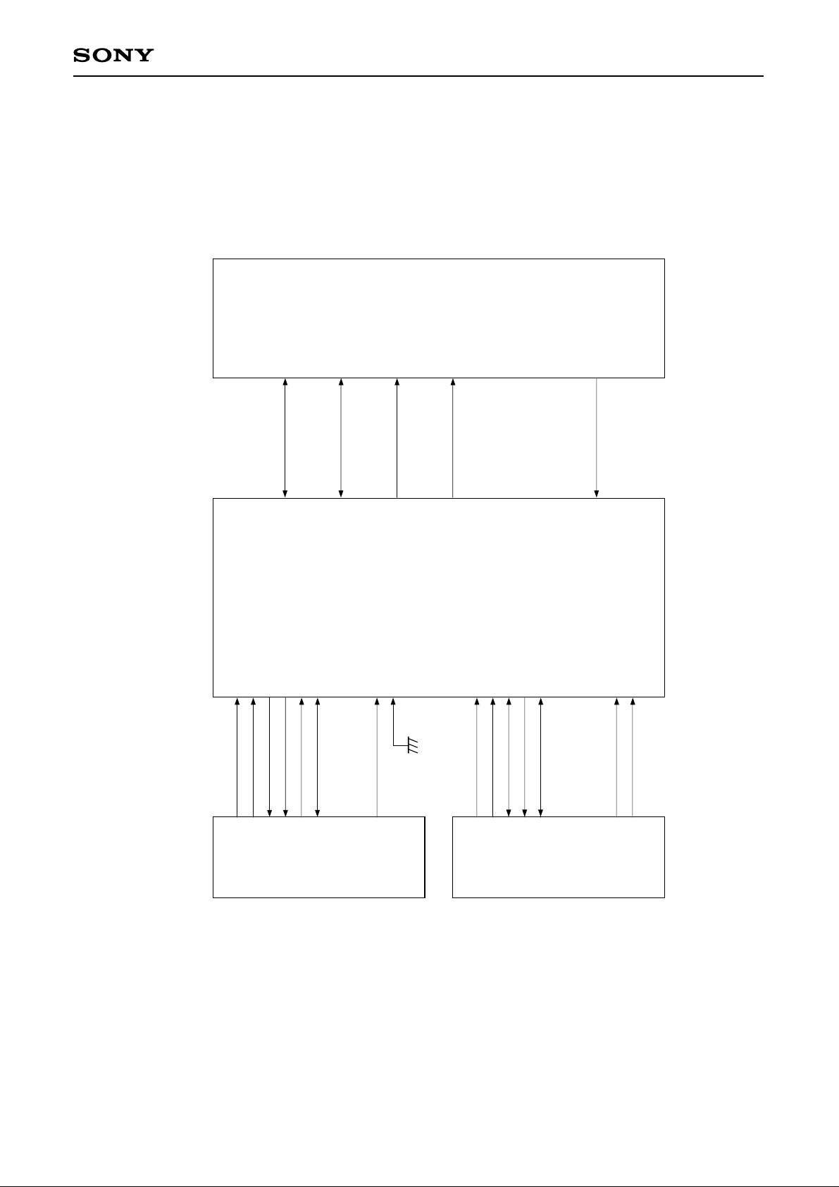
PHY LSI
IEEE1394
CXD1948R
XCS
XW/R
XWAIT
D [0 : 3]
XINT
CTL [0 : 1]
DATA [7 : 0]
ADDRESS [6 : 0]
LREQ
X8/16
XRESET
LPS
CXD1948R
AIWRITE
AIREAD
READREQ
PACKETEN
AIDT [7 : 0]
SYSCLK
IOEC
PACKETGAP
10. System Configuration Example
HOST Interface 8bit
Application Interface 8bit/asynchronous/ERRFLAG not used
HOST
– 75 –
MPEG2
Transporter
Page 76

Annex. Corresponding Table for CFR Access Address And Host Interface I/O Data (8-bit Mode)
CXD1948R
6543210765432107654321076543210
7
03h
07h
0bh
0fh
13h
17h
1bh
1fh
23h
27h
2bh
2fh
33h
37h
3bh
3fh
43h
47h
4bh
4fh
53h
67h
6bh
6fh
73h
77h
7fh
02h
06h
0ah
0eh
12h
16h
1ah
1eh
22h
26h
2ah
2eh
32h
36h
3ah
3eh
42h
46h
4ah
4eh
52h
66h
6ah
6eh
72h
76h
7eh
01h
05h
09h
0dh
11h
15h
19h
1dh
21h
25h
29h
2dh
31h
35h
39h
3dh
41h
45h
49h
4dh
51h
65h
69h
6dh
71h
75h
7dh
00h
04h
08h
0ch
10h
14h
18h
1ch
20h
24h
28h
2ch
30h
34h
38h
3ch
40h
44h
48h
4ch
50h
64h
68h
6ch
70h
74h
7ch
I/O data bit
Version
Node Address
Control
Interrupt
Interrupt Mask
Cycle Timer
DIF Mode
Iso TxRx Init
Diagnostics
Async Status
Phy Chip Access
Parallel Port
Tx1394Hdr
TxCIPHdr1
TxCIPHdr2
SPH-rsv/AddData1 to 2
AddData3 to 6
AddData7 to 10
Rx1394Hdr
RxCIPHdr1
RxCIPHdr2
IPB Write (first)
IPB Write
IPB Write (confirm)
ATF Write (first)
IPB Write ARF Read
ATF Write (confirm)
– 76 –
Page 77
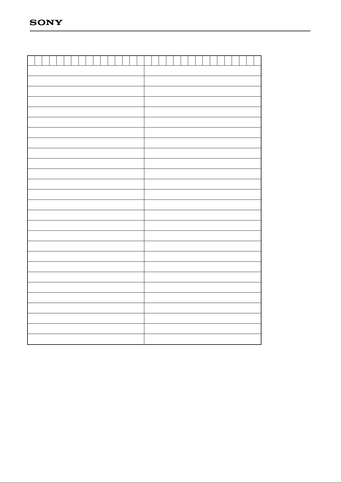
Annex. Corresponding Table for CFR Access Address And Host Interface I/O Data (16-bit Mode)
CXD1948R
1413 1211 10
15
9876543210
02h
06h
0ah
0eh
12h
16h
1ah
1eh
22h
26h
2ah
2eh
32h
36h
3ah
3eh
42h
46h
4ah
4eh
52h
66h
6ah
6eh
72h
76h
7eh
15 1413 12 1110
9876543210
00h
04h
08h
0ch
10h
14h
18h
1ch
20h
24h
28h
2ch
30h
34h
38h
3ch
40h
44h
48h
4ch
50h
64h
68h
6ch
70h
74h
7ch
I/O data bit
Version
Node Address
Control
Interrupt
Interrupt Mask
Cycle Timer
DIF Mode
Iso TxRx Init
Diagnostics
Async Status
Phy Chip Access
Parallel Port
Tx1394Hdr
TxCIPHdr1
TxCIPHdr2
SPH-rsv/AddData1 to 2
AddData3 to 6
AddData7 to 10
Rx1394Hdr
RxCIPHdr1
RxCIPHdr2
IPB Write (first)
IPB Write
IPB Write (confirm)
ATF Write (first)
IPB Write ARF Read
ATF Write (confirm)
– 77 –
Page 78
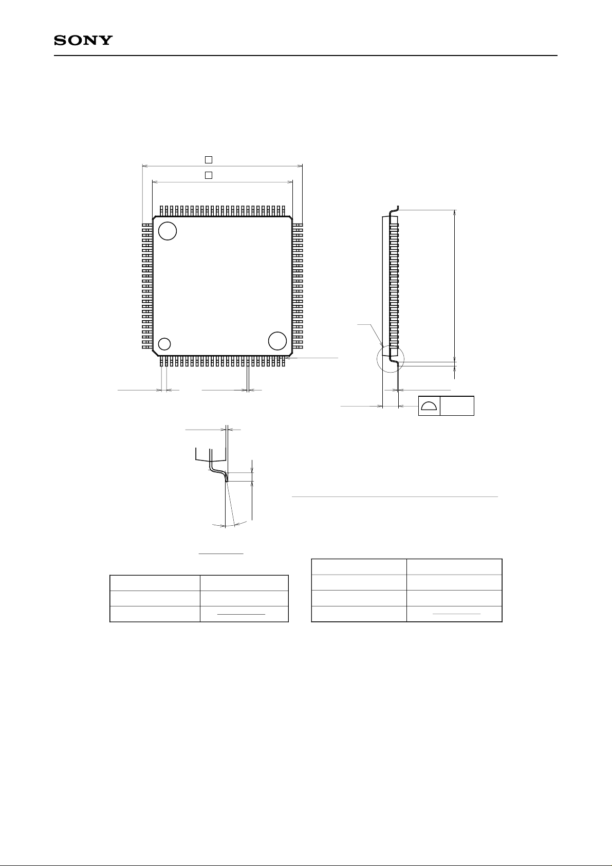
Package Outline Unit: mm
CXD1948R
100PIN LQFP (PLASTIC)
16.0 ± 0.2
∗ 14.0 ± 0.1
76
100
0.5 ± 0.08
75
1
0.18 – 0.03
0.1 ± 0.1
+ 0.08
51
50
(15.0)
A
25
26
(0.22)
+ 0.2
1.5 – 0.1
0.127 – 0.02
0.5 ± 0.2
+ 0.05
0.1
NOTE: Dimension “∗” does not include mold protrusion.
SONY CODE
EIAJ CODE
JEDEC CODE
0° to 10°
DETAIL A
LQFP-100P-L01
∗QFP100-P-1414-A
0.5 ± 0.2
PACKAGE STRUCTURE
PACKAGE MATERIAL
LEAD TREATMENT
LEAD MATERIAL
PACKAGE WEIGHT
EPOXY/PHENOL RESIN
SOLDER PLATING
42 ALLOY
– 78 –
 Loading...