

Page 1

MPEG1 Decoder
For the availability of this product, please contact the sales office.
Description
The CXD1852Q is a single-chip MPEG1 decoder
with a built-in CD-ROM decoder which allows
decoding of MPEG1 system, video and audio layers.
A built-in CD-ROM decoder enables direct connection
with a CD-DSP. Combining this chip with a control
microcomputer and 4-Mbit DRAM, etc. allows
configuration of a MPEG1 decoding system for video
CD players, etc.
Features
• Supply voltage: 3.3 ± 0.3V
• Input and output voltages: LVTTL compatible
• 5V can be applied as the input voltage (excluding
some pins)
• Allows decoding of MPEG1 system, video and
audio layers
• Built-in CD-ROM decoder allows direct connection
with a CD-DSP
• CD-ROM decoded output can be transferred to
and stored in an external DRAM
• RGB and YCbCr video data output allowed
• Built-in video sync generator
• Audio data output can support various DAC
• Supports various special playback modes
• Video CD PAL high resolution still picture can be
decoded with a single 4-Mbit DRAM
• 8-bit parallel and 4-line serial host interfaces
• CD-DA through operation allowed
CXD1852Q
120 pin QFP (Plastic)
Structure
Silicon gate CMOS IC
Applications
Video CD players, MPEG1 decoder boards, etc.
Block Diagram
CD-DSP
I/F
Sony reserves the right to change products and specifications without prior notice. This information does not convey any license by
any implication or otherwise under any patents or other right. Application circuits shown, if any, are typical examples illustrating the
operation of the devices. Sony cannot assume responsibility for any problems arising out of the use of these circuits.
CD-ROM
Decoder
To each circuit block
Host
interface
I/F
Host
MPEG
System
Decoder
DRAM
Controler
DRAM
I/F
MPEG
Audio
Decoder
MPEG
Video
Decoder
Video Postprocessor
&
Sync Generator
Signal
Video Sync
Audio
I/F
Video
I/F
– 1 –
E96656-PS
Page 2

1. Pin Configuration
CXD1852Q
VSS
XTL0O
XTL0I
DD
V
HA2
HA3
HD0
HD1
HD2
HD3
HD4
HD5
HD6
DD
V
VSS
HD7
MA3
MA4
MA2
MA5
MA1
SS
V
MA6
MA0
BC
TCKI
TDI
TENA1
TDO
VST
10
11
12
13
14
15
16
17
18
19
20
21
22
25
26
27
28
29
30
23
24
HA1
119120
HA0
118
XRST
117
HRW
XHIRQ
116
115
XHDT
114
XHCS
113
DOIN
112
BCKI
111
DATI
110
LRCI
109
C2PO
108
DD
V
XTL2I
106
107
SS
V
XTL2O
105
104
DD
BCKO
FSXI
V
103
102
101
LRCO
100
DATO
99
DOUT
98
XSGRST
CLK0O
97
CSYNC
96
FID/FHREF
CBLNK/FSC
95
94
93
1
2
3
4
5
6
7
8
9
HSYNC
VSYNC
92
91
SS
V
DD
V
90
89
DCLK
B/Cb7
88
B/Cb6
87
B/Cb5
86
B/Cb4
85
84
B/Cb3
B/Cb2
83
82
B/Cb1
81
B/Cb0
G/Y7
80
G/Y6
79
G/Y5
78
G/Y4
77
G/Y3
76
SS
V
75
VDD
74
G/Y2
73
G/Y1
72
G/Y0
71
R/Cr7
70
R/Cr6
69
R/Cr5
68
R/Cr4
67
R/Cr3
66
65
R/Cr2
R/Cr1
64
R/Cr0
63
XVOE
62
SS
V
61
313233
SS
V
MA7
34
MA8
35
XRAS
37
36
XMWE
XCAS2/MA9
38
MD7
XCAS0
39
40
MD8
41 42
MD6
MD9
43
MD5
44
MD10
45
DD
V
– 2 –
46
SS
V
MD4
47
48
MD11
49
MD3
50
MD12
51
MD2
52
MD13
MD1
53
54
MD14
55
MD0
56
MD15
57
OSDB
OSDEN
58
59
OSDR
OSDG
60
DD
V
Page 3

2. Pin Description
Pin No. Symbol I/O Description
CXD1852Q
2
3
5, 6, 119,
120
7 to 13,
16
17 to 21,
23, 24,
32, 33
34
35
36
VDD
VSS
XTL0O
XTL0I
HA0 to HA3
HD0 to HD7
MA0 to MA8
XRAS
XMWE
XCAS2/
MA9
O
I
I
I/O
O
O
O
O
+3.3V power supply
Connect to ground.
Video decoder master clock. Input the clock to XTL0I or connect an
oscillator between XTL0I and XTL0O. The recommended frequencies are
27MHz, 28.6363MHz (NTSC 8fsc) and 35.4686MHz (PAL 8fsc).
When the host interface operates in parallel mode, these pins are the
register address inputs. In serial mode, HA0 is the serial data input, and
HA1 to HA3 should be fixed to low level.
When the host interface operates in parallel mode, these pins are the
register data I/Os. In serial mode, HD0 is the serial data output, and HD1
to HD7 should be fixed to low level.
DRAM address signal outputs. Connect to the DRAM address pins so that
the numbers match.
Row address strobe signal output. Connect to the DRAM RAS signal pin.
DRAM write enable signal output. Connect to the DRAM WE signal pin.
Used when connecting 8 Mbits of DRAM. Connect to the upper word
(256K to 512K-1) DRAM CAS signal pin (for both the upper and lower
bytes) when the DRAM configuration is 256 Kwords × 16 bits × 2, and to
the MA9 pin (for two DRAMs) when the DRAM configuration is 512 Kwords
× 8 bits × 2.
37
38 to 43,
46 to 55
56
57 to 59
62
63 to 70
71 to 73,
76 to 88
81 to 88
XCAS0
MD0 to
MD15
OSDEN
OSDB,
OSDG,
OSDR
XVOE
R/Cr0 to
R/Cr7
G/Y0 to
G/Y7
B/Cb0 to
B/Cb7
O
I/O
I
I
I
O
DRAM column address strobe signal output. Connect to the lower word
(0 to 256K-1) DRAM CAS signal pin (for both the upper and lower bytes)
when the DRAM configuration is 256Kwords × 16 bits × 2, and to all
DRAM CAS signal pins in all other cases.
DRAM data signal I/Os. Connect to the DRAM data pins so that the
numbers match.
OSD enable signal. The enabled polarity is changed by the register
settings.
OSD data inputs. When the signal input to the OSDEN pin is enabled, the
color registered in the color table which is specified by these three inputs
(3 bits) is output as the image data.
Video output enable signal. Image data output and DCLK output are
enabled when this pin is low, and disabled when this pin is high (high
impedance). Note that the output control register must be set to output
enable for output to be enabled.
Image data outputs. The output data format (RGB, YCbCr, etc.) and the
correspondence between the pins and output data can be changed by
setting the registers.
89
DCLK
I/O
Dot clock (DCLK) signal. The DCLK frequency is normally 13.5MHz.
DCLK can be input from this pin, or frequency divided from the clock input
and output from this pin.
– 3 –
Page 4

Pin No. Symbol I/O Description
Horizontal sync signal. When using the built-in sync generator, the dot
92
HSYNC
I/O
clock (DCLK) is frequency divided and output. When not using the sync
generator, this pin is an input.
Vertical sync signal. When using the built-in sync generator, the dot clock
93
VSYNC
I/O
(DCLK) is frequency divided and output. When not using the built-in sync
generator, this pin is an input.
Field identification signal (FID) and horizontal sync phase reference signal
(FHREF). The signal to be used is set in the register. When set to FID, this
pin is an output if using the built-in sync generator, and an input if not
94
FID/FHREF
I/O
using the built-in sync generator. High corresponds to odd fields. When set
to FHREF, this pin outputs the signal obtained by frequency dividing XTL0.
When XTL0 is 8fsc, this signal is equivalent to the HSYNC cycle, and can
be used for phase comparison with the HSYNC signal.
Composite blanking signal (CBLNK) and fsc signal. The signal to be used
is set in the register. When set to CBLNK, this pin is an output if using the
built-in sync generator, and an input if not using the built-in sync generator.
When set to fsc, this pin outputs the signal obtained by frequency dividing
95
CBLNK/
FSC
I/O
XTL0. The frequency division ratio can be selected from 1/8 or 1/16.
CXD1852Q
96
97
98
99
100
101
102
103
106
107
109
110
CSYNC
XSGRST
CLK0O
DOUT
DATO
LRCO
BCKO
FSXI
XTL2O
XTL2I
C2PO
LRCI
Composite sync signal obtained by frequency dividing DCLK. This pin
O
cannot be input.
Sync generator reset signal input. The built-in sync generator is initialized
I
by setting this pin low.
Output for clock obtained by frequency dividing XTL0. The frequency
O
division ratio can be selected from 1, 1/2, 1/4 or 1/8.
Audio digital output.
O
Audio serial data output to DAC.
O
L/R clock output to DAC.
O
Bit clock output to DAC.
O
Audio interface clock input. Input 256fs (11.2896MHz), 384fs
I
(16.9344MHz), 512fs (22.5792MHz), or 768fs (33.8688MHz), etc.
Master clock for CD-ROM and audio decoders. Input the clock to XTL2I or
O
connect an oscillator between XTL2I and XTL2O. The recommended
frequency is 45MHz. Note that this clock is for the internal circuits, and the
I
input and output are not synchronized.
C2 pointer input from CD-DSP. Indicates that the DATI input contains an
I
error.
LR clock input from CD-DSP. Indicates the L or R channel of DATI.
I
111
112
113
114
115
DATI
BCKI
DOIN
XHCS
XHDT
I/O
Serial data input from CD-DSP.
I
Bit clock input from CD-DSP. This clock strobes the DATI input.
I
Digital data input from CD-DSP.
I
Chip select signal input during register access.
I
Wait signal output during register access. This pin is valid only when the
host interface operates in parallel mode. This pin functions as an open
drain, and should therefore be pulled up. It should be pulled up when the
host interface operates in serial mode as well.
– 4 –
Page 5

Pin No. Symbol I/O Description
CXD1852Q
116
117
118
25
26
27
28
29
30
HRW
XHIRQ
XRST
BC
TCKI
TDI
TENA1
TDO
VST
R/W signal input when the host interface operates in parallel mode. Serial
I
clock input in serial mode.
Interrupt request signal output. This pin functions as an open drain, and
O
should therefore be pulled up.
Hardware reset signal input. All operation is initialized by setting this pin
I
low.
Test. Leave open.
—
Test. Leave open.
—
Test. Leave open.
—
Test. Leave open.
—
Test. Leave open.
—
Test. Connect to ground.
—
– 5 –
Page 6

3. Electrical Characteristics
3-1. Absolute Maximum Ratings (Ta = 25°C, VSS = 0V)
CXD1852Q
Item
Supply voltage
Input pin voltage
Input pin voltage
Output pin voltage
Output pin voltage
I/O pin voltage
Allowable power dissipation
Operating temperature
Storage temperature
∗1
XTL0I and XTL2I pins
∗2
Input pins other than those in ∗1above.
∗3
XTL0O and XTL2O pins
∗4
Output pins other than those in ∗3above.
Symbol Rating Unit Remarks
VDD
VI
VI
VO
VO
VI/O
PD
Topr
Tstg
–0.5 to +4.6
–0.5 to VDD + 0.5
–0.5 to +5.5
–0.5 to VDD + 0.5
–0.5 to +5.5
–0.5 to +5.5
1.0
–20 to +75
–55 to +150
V
V
V
V
V
V
W
°C
°C
∗1
∗2
∗3
∗4
3-2. Recommended Operating Conditions (Ta = –20 to +75°C, VSS = 0V)
Item
Supply voltage
High level input voltage
High level input voltage
Low level input voltage
Input rise time
Input fall time
Operating temperature
∗1
XTL0I and XTL2I pins
∗2
I/O pins and input pins other than those in ∗1above.
Symbol Min.
VDD
VIH
VIH
VIL
Tr
Tf
Topr
3.0
2.2
2.2
0
0
0
–20
Typ.
3.3
—
—
—
—
—
—
Max.
3.6
VDD
5.0
0.8
50
50
75
Unit Remarks
V
∗1
V
∗2
V
V
ns
ns
°C
– 6 –
Page 7

CXD1852Q
3-3. DC Characteristics (Ta = –20 to +75°C, VSS = 0V, VDD = 3.3 ±0.3V)
Item
Average operating
supply current
Input leak current
High level output voltage
High level output voltage
Low level output voltage
Low level output voltage
Output leak current
Feedback resistance
Logic threshold value
High level output voltage
Low level output voltage
∗1
Input pins other than XTL0I and XTL2I
∗2
I/O pins and output pins other than XTL0O and XTL2O
∗3
Oscillators (between XTL0I and XTL0O, and between XTL2I and XTL2O)
∗4
XTL0I and XTL2I pins
∗5
XTL0O and XTL2O pins
Symbol
IDD
II
VOH
VOH
VOL
VOL
IOZ
RFB
LVth
VOH
VOL
Measurement conditions Min.
—
VI = 0 to 5.0V
IOH = –2mA
IOH = –100µA
IOL = 4mA
IOL = 100µA
VO = 0 to 5.0V,
output disabled status
VI = 0V or VI = VDD
–40
VDD – 0.8
—
—
—
–40
250k
—
IOH = –12mA
IOL = 12mA
VDD/2
—
Typ.
—
—
—
VDD – 0.4
—
0.04
—
1M
VDD/2
—
—
Max.
100
40
—
—
0.4
—
40
2.5M
—
—
VDD/2
Unit Remarks
mA
∗1
µA
∗2
V
∗2
V
∗2
V
∗2
V
∗2
µA
∗3
Ω
∗4
V
∗5
V
∗5
V
3-4. Clock Signal AC Characteristics
tCX0
tWLX0
XTL0I tWHX0
tCX2
tWLX2
XTL2I tWHX2
Item
XTL0I frequency
XTL0I cycle
XTL0I high level interval
XTL0I low level interval
XTL2I frequency
XTL2I cycle
XTL2I high level interval
XTL2I low level interval
∗1
When using in combination with the XTL0O pin as an oscillator, the maximum oscillation frequency is 50MHz.
∗2
When using in combination with the XTL2O pin as an oscillator, the maximum oscillation frequency is 50MHz.
Symbol Min.
fX0
tCX0
tWHX0
tWLX0
fX2
tCX2
tWHX2
tWLX2
—
33.3
10
10
44.7
—
8
8
Typ.
—
—
—
—
45.1584
22.2
—
—
Max.
60
—
—
—
45.4
—
—
—
Unit Remarks
MHz
ns
ns
ns
MHz
ns
ns
ns
∗1
∗1
∗2
∗2
– 7 –
Page 8

3-5. Host Interface AC Characteristics
3-5-1. Serial Mode (write, read)
XHCS
CXD1852Q
tSCS tWLSK tCSK
HRW
(SCK)
tSSI tHSI
HA0
(SI)
HD0
(SQ)
Item
Serial clock frequency
Serial clock cycle
Serial clock high level interval
Serial clock low level interval
Chip select setup time
Chip select hold time
Serial input setup time
tWHSK
tDSQtLZSQ
Symbol Min.
fSK
tCSK
tWHSK
tWLSK
tSCS
tHCS
tSSI
—
500
100
100
0
500
30
Max.
2
—
—
—
—
—
—
tHCS
tOHSQ
Unit Remarks
MHz
ns
ns
ns
ns
ns
ns
tHZSQ
Serial input hold time
Serial output enable time
Serial output determination time
Serial output hold time
Serial output disable time
tHSI
tLZSQ
tDSQ
tOHSQ
tHZSQ
30
0
—
5
0
—
15
40
—
15
ns
ns
ns
ns
ns
– 8 –
Page 9

3-5-2. Parallel Mode, Register Write
HA0 to 3
tSA
tWCSH
XHCS
XHRW
CXD1852Q
tHA
tWWL1
XHDT
HD0 to 7
Item
Address setup time
Address hold time
Chip disable time
Write pulse width
Write pulse hold time
Wait signal delay time
HD output disable time (for WR)
HD input setup time
HD input hold time
tDWA1
Symbol Min.
tSA
tHA
tWCSH
tWWL1
tHW1
tDWA1
tHZQ2
tSD1
tHD1
20
20
20
60
10
—
—
25
25
tHW1
tSD1 tHD1tHZQ2
Max.
—
—
—
—
—
15
15
—
—
inputoutput
Unit Remarks
ns
ns
ns
ns
ns
ns
ns
ns
ns
∗1
∗2
∗3
∗2, ∗4
∗1, ∗4
∗5
∗2
∗2
∗1
Specified for the edge of XHCS or HRW, whichever is later.
∗2
Specified for the edge of XHCS or HRW, whichever is earlier.
∗3
Interval during which both XHCS and HRW are low.
∗4
Applies only to access resulting in wait status.
∗5
Do not apply data while output is enabled.
– 9 –
Page 10
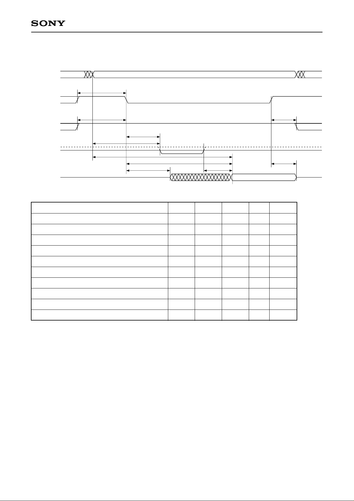
3-5-3. Parallel Mode, Register Read
HA0 to 8
tWCSH
XHCS
(CS)
CXD1852Q
tSR
XHRW
(WR)
tDWA3
XHDT
(WAIT)
HD0 to 7
Item
Chip disable time
Read setup time
Read hold time
Wait signal delay time (for CE)
Wait signal delay time (for HA)
HD output enable time (for CE)
HD output determination time (for CE)
HD output determination time (for HA)
HD output determination time (for WAIT)
tDWA2
tLZQ1
tDQ1
Symbol Min.
tWCSH
tSR
tHR
tDWA2
tDWA3
tLZQ1
tDQ1
tDQ2
tDQ4
20
10
10
—
—
0
—
0
—
tDQ2
tDQ4
Max.
—
—
—
15
15
—
60
60
30
tHR
tHZQ1
valid output
Unit Remarks
ns
ns
ns
∗1
ns
∗1
ns
∗2
ns
∗3
ns
∗3
ns
∗3, ∗4
ns
HD output disable time (for CE)
∗1
Applies only to access resulting in wait status. XHDT goes low at the later timing of CE or HA.
∗2
HD output is enabled when both conditions are met.
∗3
HD output is determined when all conditions are met.
∗4
Applies only to access resulting in wait status.
tHZQ1
—
15
ns
– 10 –
Page 11
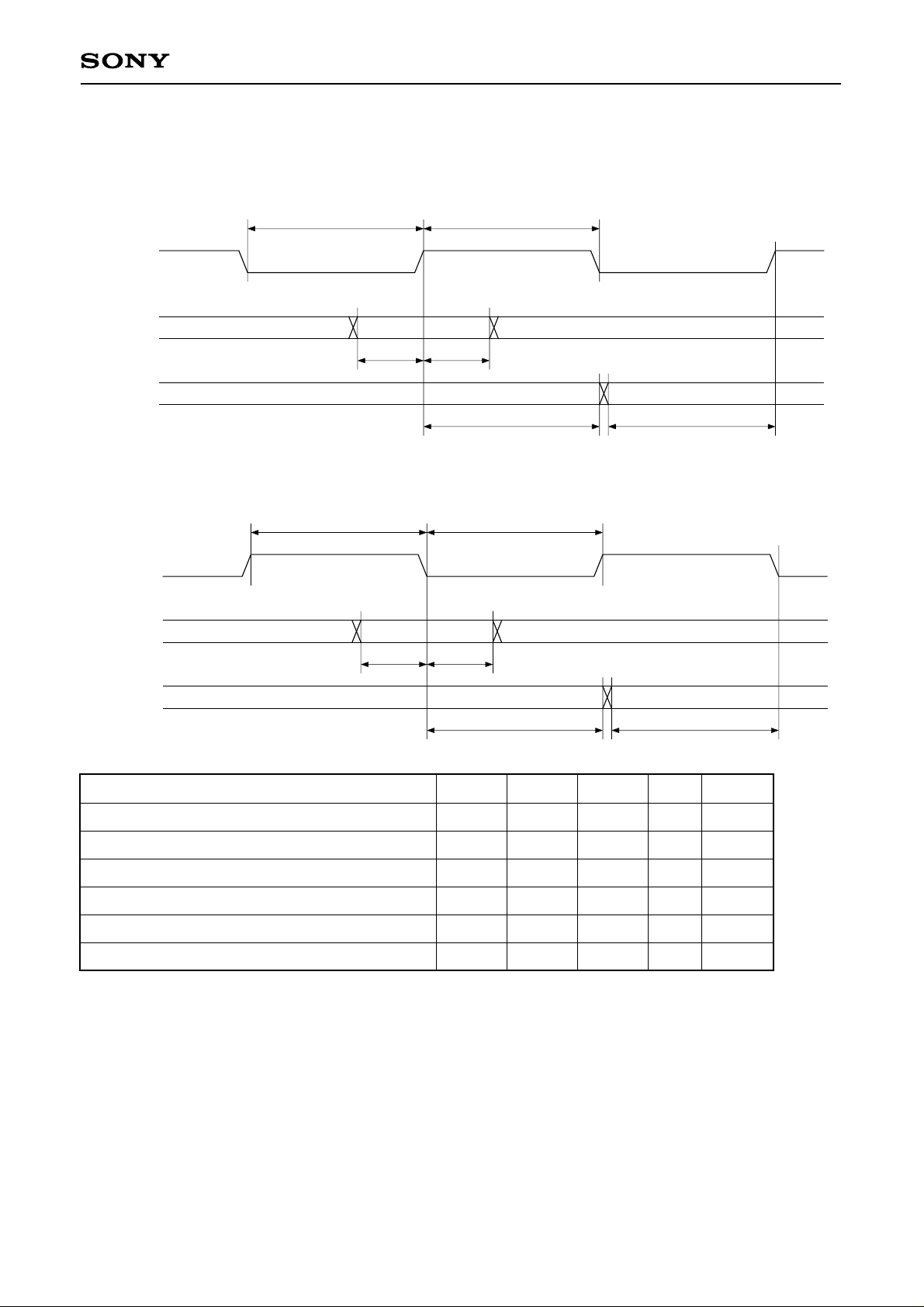
3-6. Interface for CD Signal Processing LSI
BCKFEDG = 0
tBCKI tBCKI
BCKI
DATI
LRCI, C2PO
BCKFEDG = 1
CXD1852Q
tHBC1tSBC1
tSBC2tHBC2
BCKI
DATI
LRCI, C2PO
Item
BCKI frequency
BCKI pulse width
DATI setting time (for BCKI)
DATI hold time (for BCKI)
LRCI, C2PO setting time (for BCKI)
LRCI, C2PO hold time (for BCKI)
tBCKI tBCKI
tHBC1tSBC1
Symbol Min.
fBCKI
tBCKI
tSBC1
tHBC1
tSBC2
tHBC2
87
20
20
20
20
Max.
5.7
—
—
—
—
—
tSBC2tHBC2
Unit Remarks
MHz
ns
ns
ns
ns
ns
– 11 –
Page 12
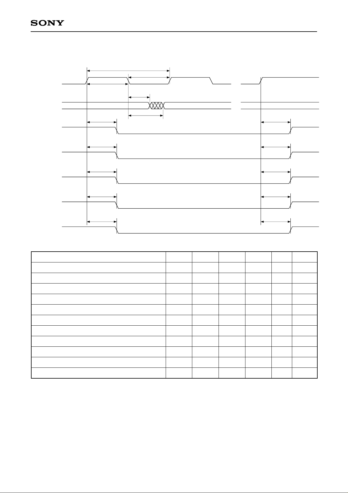
3-7. Image Data Output, Video Sync Signal Output AC Characteristics
tCDCK
tWLDCK
DCLK
R/Cr0 to 7
G/Y0 to 7
B/Cb0 to 7
HSYNC
tWHDCK
tHPD
tDPD
tDHSY
DHSY
t
CXD1852Q
tDVSY
VSYNC
tDCSY
CSYNC
tDCBL
CBLNK
tDFID
FID
Item
DCLK frequency
DCLK cycle
DCLK high level interval
DCLK low level interval
Image data output determination time
Symbol Min.
fDCK
tCDCK
tWHDCK
tWLDCK
tDPD
—
—
—
—
—
Typ.
13.5
74.1
37
37
—
Max.
—
—
—
—
15
DVSY
t
DCSY
t
DCBL
t
DFID
t
Unit Remarks
ns
ns
ns
ns
∗1
∗1
∗1
∗1
∗1, ∗2
MHz
∗1, ∗2
Image data output hold time
HSYNC output delay time
VSYNC output delay time
CSYNC output delay time
CBLNK output delay time
FID output delay time
∗1
When both inputting and outputting DCLK. For output, a load of 75pF is connected to DCLK.
∗2
The chart shows the case where the pixel data output is synchronized to the fall of DCLK, but is also the
tHPD
tDHSY
tDVSY
tDCSY
tDCBL
tDFID
—
—
—
—
—
0
—
—
—
—
—
—
—
30
30
30
30
30
ns
ns
ns
ns
ns
ns
∗1
∗1
∗1
∗1
∗1
same when synchronized to the rise of DCLK.
– 12 –
Page 13
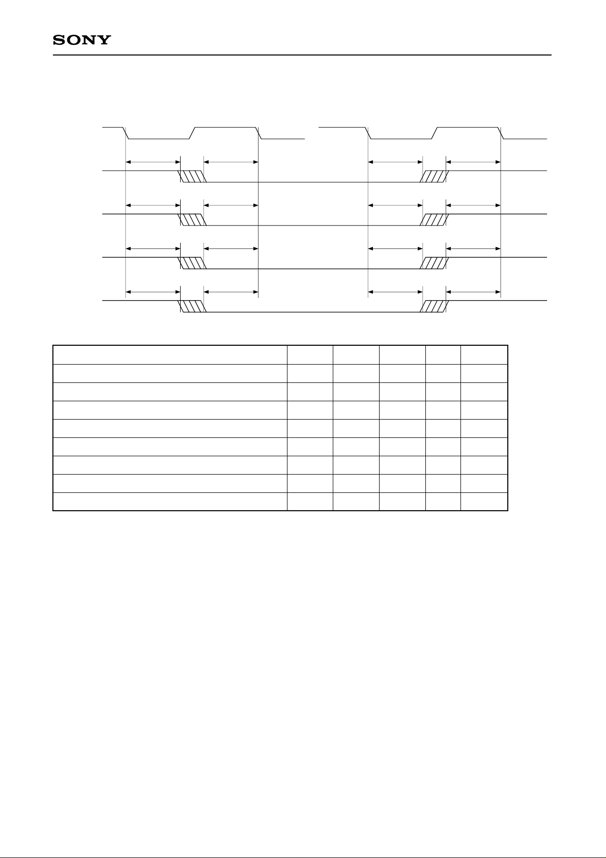
3-8. Video Sync Signal Input AC Characteristics
DCLK
CXD1852Q
HSYNC
VSYNC
CBLNK
FID
HSYNC hold time
HSYNC setup time
VSYNC hold time
VSYNC setup time
CBLNK hold time
HHSY tSHSY
t
tHVSY tSVSY
tHCBL tSCBL
tHFID tSFID
Item
Symbol Min.
tHHSY
tSHSY
tHVSY
tSVSY
tHCBL
5
5
5
5
5
HHSY tSHSY
t
tHVSY tSVSY
tHCBL tSCBL
tHFID tSFID
Max.
—
—
—
—
—
Unit Remarks
∗1
ns
∗1
ns
∗1
ns
∗1
ns
∗1
ns
CBLNK setup time
FID hold time
FID setup time
∗1
When both inputting and outputting DCLK. For output, a load of 75pF is connected to DCLK.
tSCBL
tHFID
tSFID
5
5
5
—
—
—
ns
ns
ns
∗1
∗1
∗1
– 13 –
Page 14
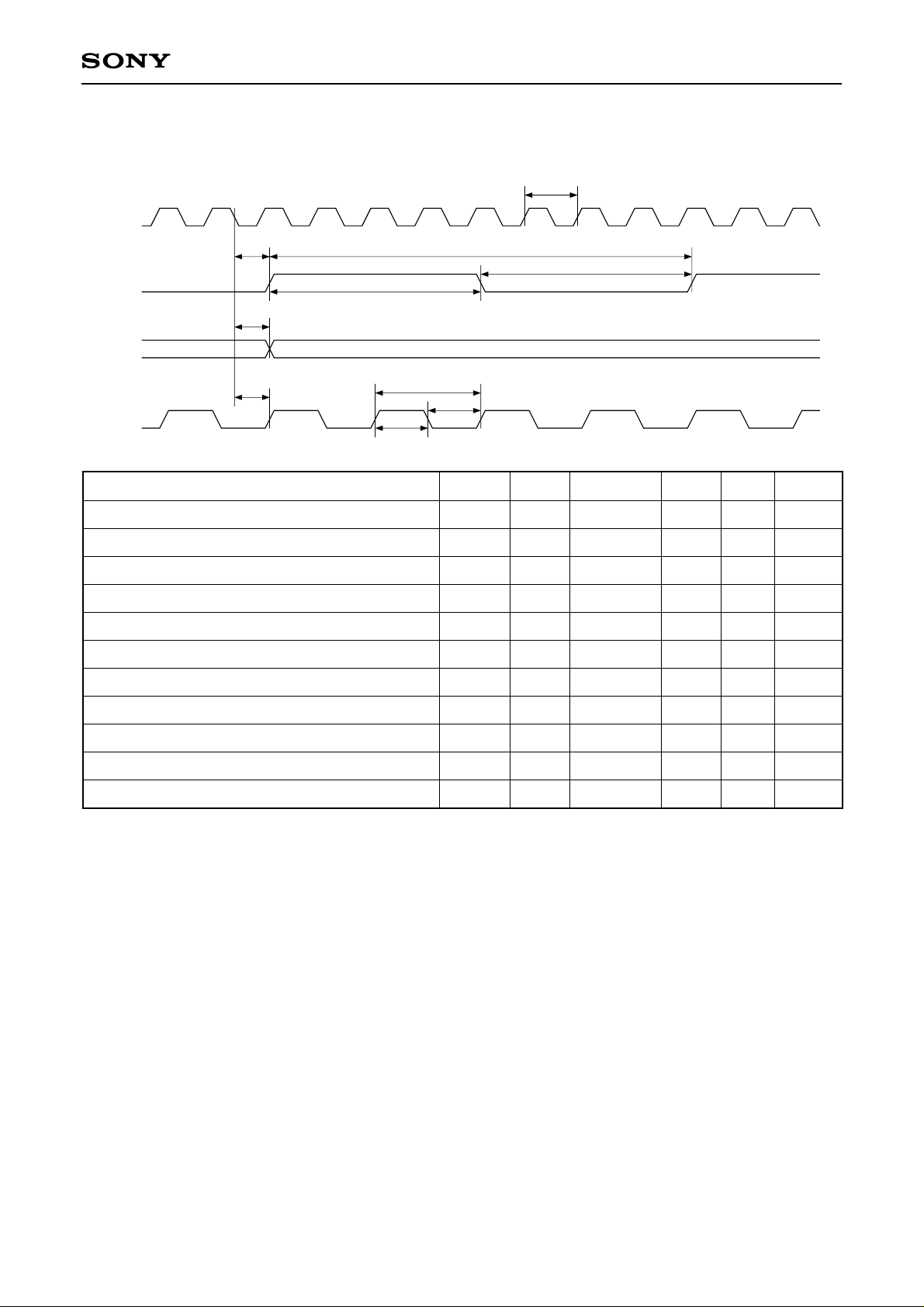
3-9. fsc System Signal Output, DCLK Output AC Characteristics
XTL0O
CXD1852Q
tCX0
tDFSC
FSC
tDFHR
FHREF
tDDCK
DCLK
Item
FSC frequency
FSC cycle
FSC high level interval
FSC low level interval
FSC output delay time
FHREF output delay time
DCLK frequency
DCLK cycle
DCLK high level interval
DCLK low level interval
DCLK output delay time
tWLFSC
tWLDCK
tCDCK
tWHDCK
Symbol Min.
fFSC
tCFSC
tWHFSC
tWLFSC
tDFSC
tDFHR
fDCK
tCDCK
tWHDCK
tWLDCK
tDDCK
tCFSC
—
—
—
—
—
—
—
—
—
—
—
tWHFSC
Typ.
1/(i × tCX0)
i × tCX0
i × tCX0/2
i × tCX0/2
1/(j × tCX0)
j × tCX0
j × tCX0/2
j × tCX0/2
—
—
—
Max.
—
—
—
—
15
15
—
—
—
—
15
Unit Remarks
∗1
∗1
∗1
∗1
ns
ns
∗2
∗2
∗2
∗2
ns
∗1
The frequency division ratio i can be selected from 8 or 16.
∗2
The frequency division ratio j can be selected from 2 or 4.
– 14 –
Page 15
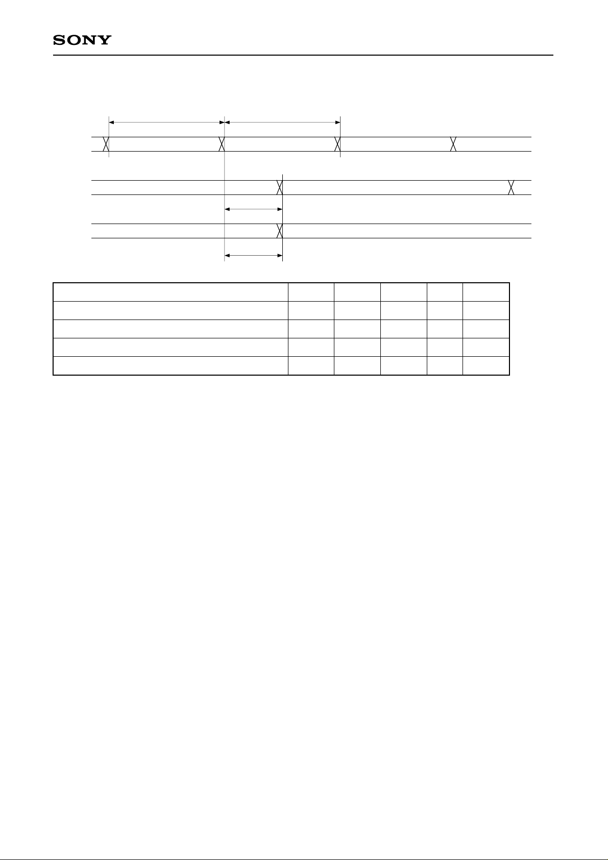
3-10. Audio Interface
BCKO
DATO
LRCO
CXD1852Q
tBCKOtBCKO
tDDAT
tDLRC
Item
BCKO frequency
BCKO pulse width
DATO delay time (for BCKO)
LRCO delay time (for BCKO)
Symbol Min.
fBCKO
tBCKO
tDDAT
tDLRC
160
—
—
Max.
3.1
—
40
40
Unit Remarks
MHz
ns
ns
ns
– 15 –
Page 16

3-11. DRAM Interface AC Characteristics
3-11-1. Write Cycle
CXD1852Q
XRAS
XCAS0 to 3
XMWE
MA0 to 9
MD0 to 15
RAS precharge time
RAS to CAS delay time
RAS hold time
Fast page mode cycle time
CAS pulse width
CAS precharge time
Item
tRP
tRCD
tWCS
tASR tRAH tASC tCAH
tDS tDH
Symbol Min.
tRP
tRCD
tRSH
tPC
tCAS
tCP
tPC
tCAS tCP tRSH
Typ.
2 × tv
2 × tv
Max.
tv
2 × tv
tv
tv
tWCH
—
—
—
—
—
—
Unit Remarks
∗2
ns
∗2
ns
∗2
ns
∗2
ns
∗2
ns
∗2
ns
Write command setup time
Write command hold time
Row address setup time
Row address hold time
Column address setup time
Column address hold time
Write data setup time
Write data hold time
∗1
tv is the basic clock cycle for the DRAM interface circuit.
∗2
Same as the DRAM interface read cycle.
tWCS
tWCH
tASR
tRAH
tASC
tCAH
tDS
tDH
tv
2 × tv
tv
tv
tv
tv
tv
tv
—
—
—
—
—
—
—
—
ns
ns
ns
ns
ns
ns
ns
ns
∗2
∗2
∗2
∗2
– 16 –
Page 17
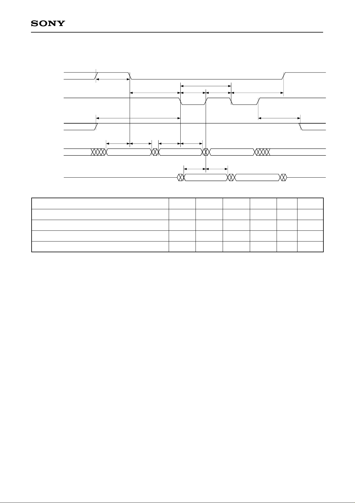
3-11-2. Read Cycle
CXD1852Q
XRAS
XCAS0 to 3
XMWE
MA0 to 9
MD0 to 15
Read command setup time
Read command hold time
Read data setup time
Read data hold time
Item
tRP
tRCD
tRCS
tASR tRAH tASC tCAH
Symbol Min.
tRCS
tRCH
tMDS
tMDH
tPC
tCAS tCP tRSH
tMDS tMDH
Typ.
Max.
4 × tv
tv
2
8
—
—
—
—
tRCH
Unit Remarks
ns
ns
ns
ns
∗1
tv is the basic clock cycle for the DRAM interface circuit.
∗2
See the DRAM interface write cycle for items which appear in the timing chart but not in the table.
– 17 –
Page 18
CXD1852Q
4. Description of Functions
4-1. Host Interface Function
• The CXD1852Q operation is controlled by writing and reading registers. Write and read can also be
performed to an external DRAM via the registers. See the separately issued Register Manual for the
relationship between the registers and operation.
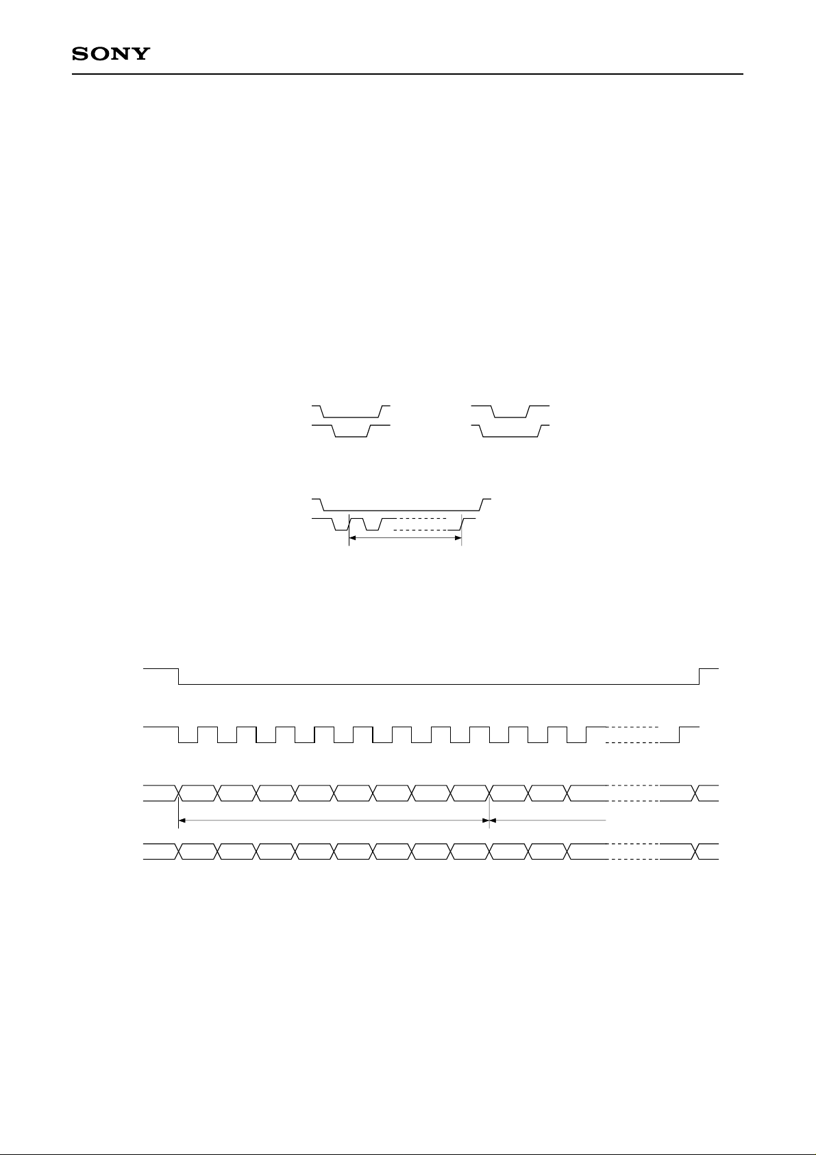
• The host interface operates while XHCS is low and does not operate while XHCS is high.
• The host interface operating mode can be set to 4-line serial or 8-bit parallel. The operating mode is selected
automatically at the end of the initial access after the hardware has been reset. (See the figure below.)
Registers are not accessed correctly until this selection has been determined, or in other words until the end
of the initial access after the hardware has been reset. Also, the HA3 to HA0 inputs should all be fixed low
during the operating mode selection access.
XHCS
HRW
XHCS
HRW
• The serial mode signal format is as follows.
XHCS
HRW
(SCK)
HA0
(SI)
bit0 bit1 bit2 bit3 bit4 bit5 bit6 bit7 bit8 bit9
byte0 byte1
XHCS
HRW
Access judged as parallel mode
8 rises
Access judged as serial mode
HD0
(SO)
bit0 bit1 bit2 bit3 bit4 bit5 bit6 bit7 bit8 bit9
1) In serial mode, input data is fetched in sync with the rise of HRW (SCK). Output data is synchronized with
the fall of HRW.
2) The initial byte (byte0) of the input after XHCS changes to low is a command. This command determines
the subsequent byte processing. See the following page for a description of commands and processing.
3) Input data is processed in one byte units. Therefore, when the final data consists of a number of bits which
is less than one byte, this deficient data is not processed. Be sure to input data with a number of bits which
is an integer multiple of 8. Also, the 0x20, 0x60, 0xA0 and 0xE0 commands process data in two byte units,
so data which is an even multiple of 8 should be input when using these commands.
– 18 –
Page 19

CXD1852Q
Command
bit7 ··· bit0
00000000
00010000
00100000
00110000
01100000
01110000
10000000
10010000
10100000
write
2nd input byte 3rd input byte 4th input byte
read
write
read
write
read
write
read
write
read
write
Register No.
+U/L byte select
Register No.
+U/L byte select
Register No.
Register No.
Register No.
Register No.
Register No.
+U/L byte select
Register No.
+U/L byte select
Register No.
Register data
don’t care
Register data
(Lower byte)
don’t care
Register data
(Lower byte)
don’t care
Register data
don’t care
Register data
(Upper byte)
Register No.
+U/L byte select
Register No.
+U/L byte select
Register data
(Upper byte)
don’t care
Register data
(Upper byte)
don’t care
Register No.
+U/L byte select
Register No.
+U/L byte select
Register data
(Lower byte)
Successive
odd-numbered
input bytes
Register data
don’t care
Register data
(Lower byte)
don’t care
Register data
(Lower byte)
don’t care
Register data
don’t care
Register data
(Upper byte)
Successive
even-numbered
input bytes
Register No.
+U/L byte select
Register No.
+U/L byte select
Register data
(Upper byte)
don’t care
Register data
(Upper byte)
don’t care
Register No.
+U/L byte select
Register No.
+U/L byte select
Register data
(Lower byte)
first
bit
LSB
first
LSB
first
LSB
first
LSB
first
LSB
first
LSB
first
MSB
first
MSB
first
MSB
first
Auto
inc.
No
No
No
No
Yes
Yes
No
No
No
10110000
11100000
11110000
read
write
read
Register No.
Register No.
Register No.
don’t care
Register data
(Upper byte)
don’t care
don’t care
Register data
(Lower byte)
don’t care
don’t care
Register data
(Upper byte)
don’t care
don’t care
Register data
(Lower byte)
don’t care
MSB
first
MSB
first
MSB
first
No
Yes
Yes
Description of Commands
1) The "write read" column indicates whether that command writes data to or reads data from the registers.
2) Bytes marked with "Register No. + U/L byte select" specify the register to be accessed as well as whether
to access the upper or lower bytes of the register. The upper 7 bits specify the register No., and the
lowermost bit specifies the upper or lower bytes. When the lowermost bit is "0", the lower bytes are
selected, when "1", the upper bytes are selected.
3) Bytes marked with "Register No." specify the register to be accessed. The upper 7 bits specify the register
No., and the lowermost bit can be either "0" or "1".
4) The "Auto inc." column indicates the presence of the register No. auto increment function. For commands
without this function, the most recently input register No. is valid. For example, in case of the command
0x00, the register data input by the odd bytes is written to the register specified by the previous byte's input.
For the command 0x20, all subsequent data is written sequentially to the register specified by the 2nd input
byte.
5) For commands with the register No. auto increment function, the register specified by the 2nd input byte is
accessed first, and then access shifts to the register No. incremented by one each time the data for one
register (2 bytes) is read or written. For example, when using the command 0x60, if 0x08 is specified by the
2nd input byte, the 3rd and 4th input bytes are written to register 0x08, and the 5th and 6th input bytes are
written to register 0x09.
6) Bytes marked with "register data" are the data to be written to the registers during write commands.
– 19 –
Page 20

CXD1852Q
7) When executing read commands, register data output starts from the 3rd output byte (bit 16). All earlier
output data is invalid data. Access shifts to a new register each time the output for one register (2 bytes) is
finished. For example, in case of the command 0x10, the byte data specified by the 2nd input byte is output
to the 3rd output byte, the other byte data in the same register is output to the 4th byte, and the byte data
specified by the 4th input byte is output to the 5th output byte.
8) The "first bit" column indicates whether LSB first or MSB first processing is performed for input or output of
the 2nd and subsequent bytes. This specification does not apply to the 1st byte (command). Commands
are normally LSB first. If LSB first is specified, processing is performed in the order where the initial bit in
each byte is LSB and the final bit is MSB. This order is reversed for MSB first. Note that for registers, bit 15
noted in the Register Manual is MSB and bit 0 is LSB.
4-2. DRAM Interface Function
• The applicable DRAMs are speed version 70 devices (RAS access time (Trac) of 70ns or less) with the fast
page mode function.
• When the total capacity of the external DRAM is 4 Mbits, use a 2CAS type DRAM with a configuration of 256
Kwords × 16 bits. When the total capacity is 8 Mbits, use two 2CAS type DRAMs with a configuration of 256
Kwords × 16 bits or 512 Kwords × 8 bits.
• Refresh is performed automatically using RAS-only-refresh. External control is not necessary.
• The DRAM is divided into the image frame memory, audio bit stream buffer, video bit stream buffer, user
data and on-memory register areas.
• The user data area can be used freely by the user, and CD-ROM decoded output can also be transferred to
this area. This area can be used to store video CD PSD, etc.
• The desired DRAM areas can be accessed from the control microcomputer via the registers.
4-3. CD-ROM Decoder Function
• CD signal processor LSI interface
The CD-ROM decoder has a CD signal processor LSI (CD-DSP) interface which directly interfaces the serial
data output from the CD-DSP. This interface supports a wide variety of input formats to enable connection
with general CD-DSP.
• CD-ROM data decoding (supports CD-ROM XA format mode2, form1 and form2)
CD-ROM data input from the CD-DSP supports CD-ROM XA format (mode2, form1 and form2).
• Input CD-ROM data is decoded by the CD-ROM decoder block. Also, the CD-DA signal input from the CD-
DSP can be output directly from the audio interface.
• The CD-ROM decoder has the following decoding and data transfer operating modes. The real-time
correction and write-only modes facilitate the loading of video CD PSD to the external DRAM, etc.
1) Auto transfer mode
The MPEG pack data within one sector of the video CD is automatically transferred to the system
decoder, where the audio stream sector or video stream sector can be decoded. This mode transfers
2324 bytes counted from the initial byte of user data within one sector to the system decoder.
2) Real-time correction mode
This mode executes error detection and correction processing for mode2, form1 sectors. The 2048 bytes
of user data within the error processed sector are transferred to the user area of the external DRAM. The
4 bytes of header information within the sector can also be loaded in the on-memory register within the
DRAM.
3) Write-only mode
This mode transfers the 2340 bytes of header, subheader and user data within one sector to the user area
of the external DRAM. When a form1 sector is input, error detection and correction processing is
performed and then the data is transferred to the buffer memory. When a form2 sector is input, the data is
transferred as is.
– 20 –
Page 21
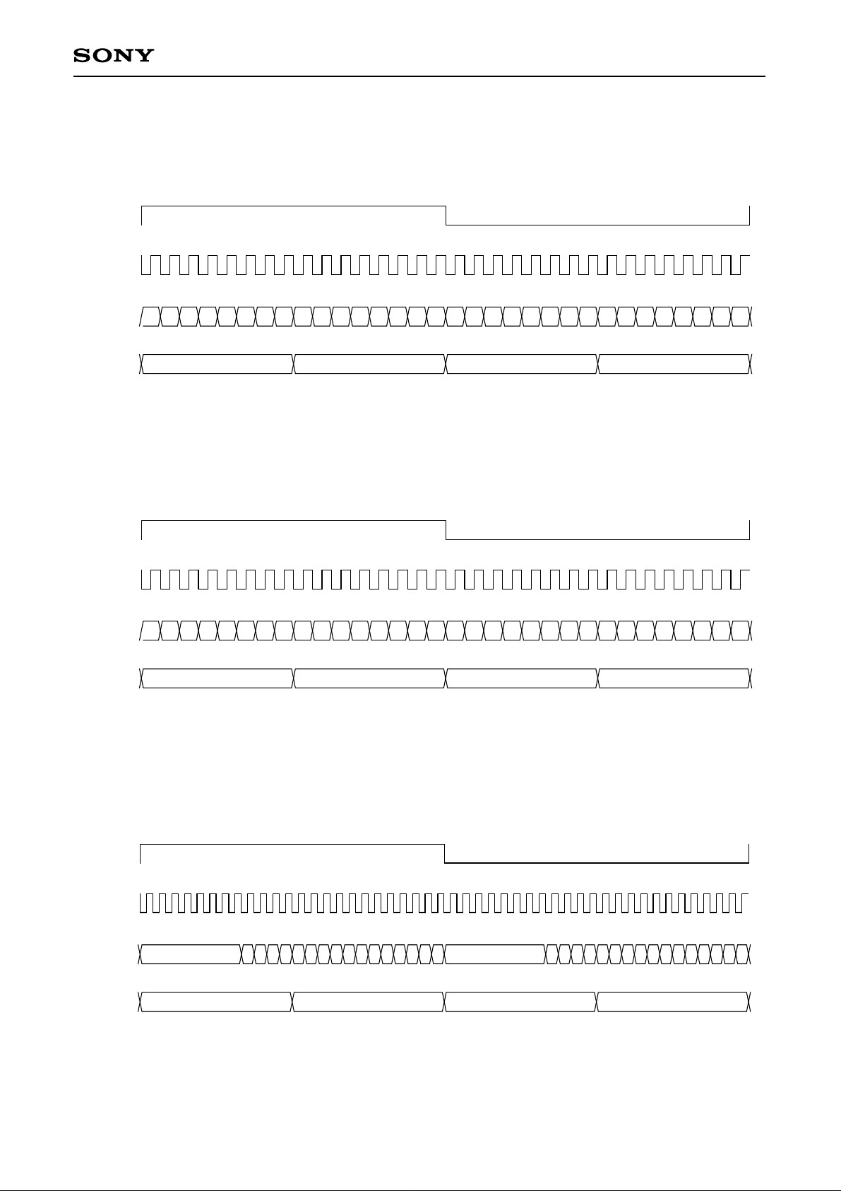
CD-DSP Input Signal Formats
1) 32-bit slot, MSB first, BCKMOD1, 0 = 00, LSBFST = 0
CXD1852Q
LRCI
BCKI
MSB LSB MSB LSB
DATI
C2PO Upper
D15 D14 D13 D12 D11 D10 D9 D8 D7 D6 D5 D4 D3 D2 D1 D0 D15 D14 D13 D12 D11 D10 D9 D8 D7 D6 D5 D4 D3 D2 D1 D0
Lch Rch
Lower Upper Lower
2) 32-bit slot, LSB first, BCKMOD1, 0 = 00, LSBFST = 1
LRCI
BCKI
DATI
LSB MSB LSB MSB
D0 D1 D2 D3 D4 D5 D6 D7 D8 D9 D10 D11 D12 D13 D14 D15 D0 D1 D2 D3 D4 D5 D6 D7 D8 D9 D10 D11 D12 D13 D14 D15
Lch Rch
3115 160
3115 160
C2PO Upper
Lower Upper Lower
3) 48-bit slot, MSB first, BCKMOD1, 0 = 01, LSBFST = 0
LRCI
BCKI
MSB LSB MSB LSB
DATI
D15D14D13D12D11D10 D9 D8 D7 D6 D5 D4 D3 D2 D1 D0 D15D14D13D12D11 D10 D9 D8 D7 D6 D5 D4 D3 D2 D1 D0
C2PO Upper
Lch Rch
Lower Upper Lower
4723 240
– 21 –
Page 22
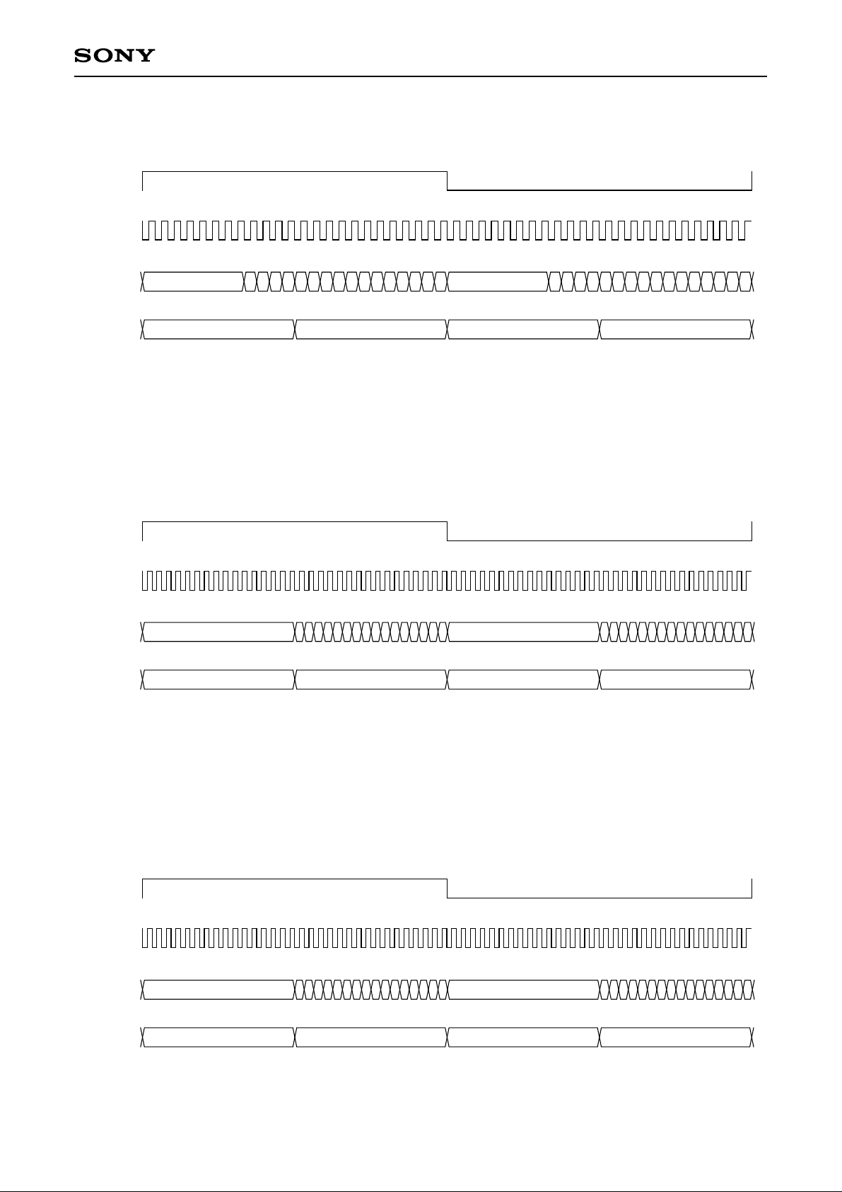
4) 48-bit slot, LSB first, BCKMOD1, 0 = 01, LSBFST = 1
CXD1852Q
LRCI
BCKI
LSB MSB LSB MSB
DATI
C2PO Upper
Lch Rch
D0 D1 D2 D3 D4 D5 D6 D7 D8 D9 D10D11D12D13D14D15 D0 D1 D2 D3 D4 D5 D6 D7 D8 D9 D10D11D12D13D14D15
Lower Upper Lower
5) 64-bit slot, MSB first, BCKMOD1, 0 = 10, LSBFST = 0
LRCI
BCKI
Lch Rch
4723 240
6331320
MSB LSB MSB LSB
DATI
C2PO Upper
don't care don't care
Lower Upper Lower
6) 64-bit slot, LSB first, BCKMOD1, 0 = 10, LSBFST = 1
LRCI
BCKI
DATI
don't care don't care
Lch Rch
LSB MSB LSB MSB
0123456789101112131415 0123456789101112131415
6331320
1514131211109876543210 1514131211109876543210
C2PO Upper
Lower Upper Lower
– 22 –
Page 23

CXD1852Q
4-4. System Decoder Function
• The MPEG1 system layer (ISO/IEC 11172-1) is decoded, the audio and video bit streams are separated, and
each bit stream is transferred to the respective bit stream buffer.
• The MPEG1 bit stream input can be selected from either the built-in CD-ROM decoder or the host interface.
• The system decoder has a 128-word (256-byte) FIFO for the bit stream input.
• Audio and video sync playback are controlled according to the time stamp within the bit stream.
4-5. Video Decoder Function
• The MPEG1 video layer (ISO/IEC 11172-2) is decoded. This function supports the range where
constrained_parameter_flag = "1" and video CD high resolution still picture.
• Video CD high resolution still picture (NTSC, PAL) can be decoded with a single external 4-Mbit DRAM.
• Special decoding functions are as follows. Slow playback, fast forward and other modes can be realized by
combining these functions.
I-Play: Only I-Pictures are decoded.
Still (Pause): Decoding is paused.
1 Frame Play: Only one frame (picture) is decoded.
IP-Play: Only I and P-Pictures are decoded.
IPB-Play: Alternate frames of continuous B-Pictures and all I and P-Pictures are decoded.
• This function supports digest play.
• The various information in the bit stream is loaded to the on-memory register area within the external DRAM.
4-6. Video Post Processor and Sync Generator Functions
• The image data output format can be selected from 24-bit RGB, 24-bit YCbCr and 16-bit YCbCr. See the
following page.
• Fade in and fade out are allowed.
• Image enlargement and reduction are allowed.
• The CXD1852Q contains an OSD color table and selector, and OSD display is achieved by inputting the
OSD character signal.
• The video sync signal can be generated using the built-in sync generator. Image data can also be output in
sync with an externally input video sync signal.
– 23 –
Page 24

DCLK
HSYNC
R0 to 7
G0 to 7
R (n)
G (n)
CXD1852Q
R (n + 1) R (0) R (1) R (2) R (3)
G (n + 1) G (0) G (1) G (2) G (3)
B0 to 7
B (n)
B (n + 1) B (0) B (1) B (2) B (3)
24-bit RGB output format
DCLK
HSYNC
Y0 to 7
Cb0 to 7
Cr0 to 7
Y (n)
Cb (n)
Cr (n)
Y (n + 1) Y (0) Y (1) Y (2) Y (3)
Cb (n + 1) Cb (0) Cb (1) Cb (2) Cb (3)
Cr (n + 1) Cr (0) Cr (1) Cr (2) Cr (3)
24-bit YCbCr output format
DCLK
HSYNC
Y0 to 7
C0 to 7
Y (n)
Cb (n)
Y (n + 1) Y (0) Y (1) Y (2) Y (3)
Cr (n) Cb (0) Cr (0) Cb (2) Cr (2)
16-bit YCbCr output format
Note)
• The subscript (i) indicates the data for pixel i.
• The above timing charts show the timing when the pixel data output is synchronized with the fall of DCLK.
The pixel data output can also be synchronized with the rise of DCLK.
– 24 –
Page 25

CXD1852Q
4-7. Audio Decoder Function
• MPEG audio stream decoding is performed for MPEG1 standard (ISO/IEC 11172-3) layer 1 and layer 2.
• Monaural, dual, stereo and joint stereo decoding modes are supported.
• All MPEG1 standard sampling frequencies (32kHz, 44.1kHz, 48kHz) are supported.
• All MPEG1 standard bit rates are supported.
Layer 1: 32Kbps (monaural/stereo) to 448Kbps (monaural/stereo)
Layer 2: 32Kbps (monaural) to 384Kbps (stereo)
• The audio decoder's audio interface output port is equipped with a PCM audio output which outputs decoded
audio data in bit serial format and a digital audio interface output (digital out). The audio interface is set by
setting the internal registers.
1) LRCK and BCK generation
The LR clock and bit clock can be generated by frequency dividing the clock input from external pins XTLI
or FSXI. The generated clocks are output from the BCKO and LRCO pins, respectively. LRCO and BCKO
can be output in the desired polarity. Also, the number of slots per sample supports the three types of 32,
48 and 64 bit clocks/LRCK.
2) PCM audio output format
The PCM audio output format can be set to any of the following combinations to allow connection with a
wide range of 1-bit D/A converters.
16-bit word length, MSB first or LSB first, frontward truncation or rearward truncation
18-bit word length, MSB first or LSB first, frontward truncation or rearward truncation
20-bit word length, MSB first or LSB first, frontward truncation or rearward truncation
24-bit word length, MSB first or LSB first, frontward truncation or rearward truncation
3) Digital out format
The digital out output format supports the type2, form1 format for consumer use. The output word length
can be selected from 16, 18, 20 or 24 bits.
4) Decoded channel assignment
Channels 1 and 0 of the audio sample obtained by decoding the MPEG audio stream can be assigned to
the L and R channel outputs in any combination.
5) Audio mute
The audio output contains a zero-cross mute circuit. Zero-cross detection is performed for 44 sample
sections (approximately 0.1ms when fs = 44.1kHz), and if zero-cross is not detected, the output is forcibly
muted.
6) Attenuator
The audio output contains an attenuator circuit. Attenuation of –12dB can be obtained by setting the
internal register.
7) CD-DA output mode
When playing back a CD-DA disc, the data input from the CD-DSP can be output directly from the PCM
audio output (DATO) and the digital audio interface output port (DOUT). Output ports LRCO and BCKO can
also select and output the clock inputs LRCI and BCKI from the CD-DSP.
– 25 –
Page 26
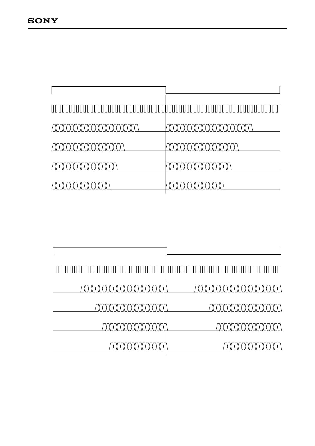
PCM Audio Output Formats
1) 64-bit slot, frontward truncation, LSB first, OSLT1, 0 = 10, OTRUNK = 1, OLSBFST = 1
CXD1852Q
LRCO
Lch Rch
BCKO
LSB MSB
LSB MSB
DATO
15141312111098765432102322212019181716
151413121110987654321019181716
15141312111098765432101716
1514131211109876543210
15141312111098765432102322212019181716
151413121110987654321019181716
15141312111098765432101716
1514131211109876543210
2) 64-bit slot, rearward truncation, LSB first, OSLT1, 0 = 10, OTRUNK = 0, OLSBFST = 1
6331 320
DAL1, 0 = 11
DAL1, 0 = 10
DAL1, 0 = 01
DAL1, 0 = 00
LRCO
BCKO
LSB
DATO
DAL1, 0 = 11
DAL1, 0 = 10
DAL1, 0 = 01
DAL1, 0 = 00
LSB/MSB first setting
OLSBF = 1: set to LSB first
OLSBF = 0: set to MSB first
Lch Rch
MSB
15141312111098765432102322212019181716
151413121110987654321019181716 151413121110987654321019181716
15141312111098765432101716 15141312111098765432101716
1514131211109876543210 1514131211109876543210
LSB MSB
Data word length setting
DAL1, 0 = 11: 24 bits
DAL1, 0 = 10: 20 bits
DAL1, 0 = 01: 18 bits
DAL1, 0 = 00: 16 bits
6331 320
15141312111098765432102322212019181716
– 26 –
Page 27
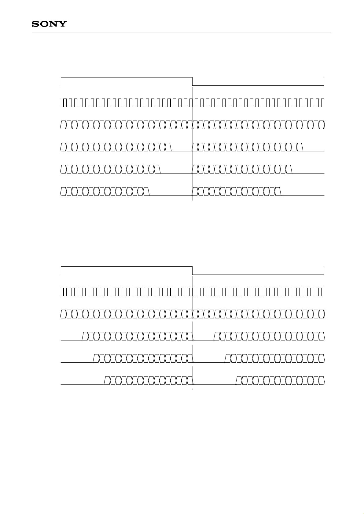
3) 48-bit slot, frontward truncation, LSB first, OSLT1, 0 = 01, OTRUNK = 1, OLSBFST = 1
CXD1852Q
LRCO
Lch Rch
BCKO
LSB MSB
LSB MSB
DATO
D0 D1 D2 D3 D4 D5 D6 D7 D8 D9 D10D11 D12D13D14D15 D16D17D18D19D20D21D22D23
D0 D1 D2 D3 D4 D5 D6 D7 D8 D9 D10D11 D12D13D14D15 D16D17D18D19 D0 D1 D2 D3 D4 D5 D6 D7 D8 D9 D10D11D12D13D14D15D16D17D18D19
D0 D1 D2 D3 D4 D5 D6 D7 D8 D9 D10D11 D12D13D14D15 D16D17
D0 D1 D2 D3 D4 D5 D6 D7 D8 D9 D10D11 D12D13D14D15
D0 D1 D2 D3 D4 D5 D6 D7 D8 D9 D10D11D12D13D14D15D16D17D18D19D20 D21D22D23
D0 D1 D2 D3 D4 D5 D6 D7 D8 D9 D10D11D12D13D14D15D16D17
D0 D1 D2 D3 D4 D5 D6 D7 D8 D9 D10D11D12D13D14D15
4) 48-bit slot, rearward truncation, LSB first, OSLT1, 0 = 01, OTRUNK = 0, OLSBFST = 1
4723 240
DAL1, 0 = 11
DAL1, 0 = 10
DAL1, 0 = 01
DAL1, 0 = 00
LRCO
BCKO
LSB MSB
DATO
D0 D1 D2 D3 D4 D5 D6 D7 D8 D9 D10D11 D12D13D14D15 D16D17D18D19D20D21D22
DAL1, 0 = 11
DAL1, 0 = 10
D0 D1 D2 D3 D4 D5 D6 D7 D8 D9 D10D11D12D13D14D15D16D17 D18 D0 D1 D2 D3 D4 D5 D6 D7 D8 D9 D10D11D12D13D14D15D16D17D18D19
DAL1, 0 = 01
D0 D1 D2 D3 D4 D5 D6 D7 D8 D9 D10D11D12D13D14D15D16 D0 D1 D2 D3 D4 D5 D6 D7 D8 D9 D10D11D12 D13D14D15D16D17
DAL1, 0 = 00
LSB/MSB first setting
OLSBF = 1: set to LSB first
OLSBF = 0: set to MSB first
Lch Rch
4723 240
LSB MSB
D1 D2 D3 D4 D5 D6 D7 D8 D9 D10D11D12D13D14D15D16D17D18 D19D20D21D22 D23
D23 D0
D19
D17
D0 D1 D2 D3 D4 D5 D6 D7 D8 D9 D10D11D12D13D14 D0 D1 D2 D3 D4 D5 D6 D7 D8 D9 D10 D11D12D13D14D15
D15
Data word length setting
DAL1, 0 = 11: 24 bits
DAL1, 0 = 10: 20 bits
DAL1, 0 = 01: 18 bits
DAL1, 0 = 00: 16 bits
– 27 –
Page 28

5) 32-bit slot, LSB first, OSLT1, 0 = 00, OLSBFST = 1
CXD1852Q
LRCO
BCKO
DATO
LSB MSB LSB MSB
D0 D1 D2 D3 D4 D5 D6 D7 D8 D9 D10 D11 D12 D13 D14 D15 D0 D1 D2 D3 D4 D5 D6 D7 D8 D9 D10 D11 D12 D13 D14 D15
Lch Rch
6) 32-bit slot, MSB first, OSLT1, 0 = 00, OLSBFST = 0
LRCO
BCKO
DATO
MSB LSB MSB LSB
D15 D14 D13 D12 D11 D10 D9 D8 D7 D6 D5 D4 D3 D2 D1 D0 D15 D14 D13 D12 D11 D10 D9 D8 D7 D6 D5 D4 D3 D2 D1 D0
Lch Rch
3115 160
3115 160
LSB/MSB first setting
OLSBF = 1: set to LSB first
OLSBF = 0: set to MSB first
Data word length: 16 bits
– 28 –
Page 29
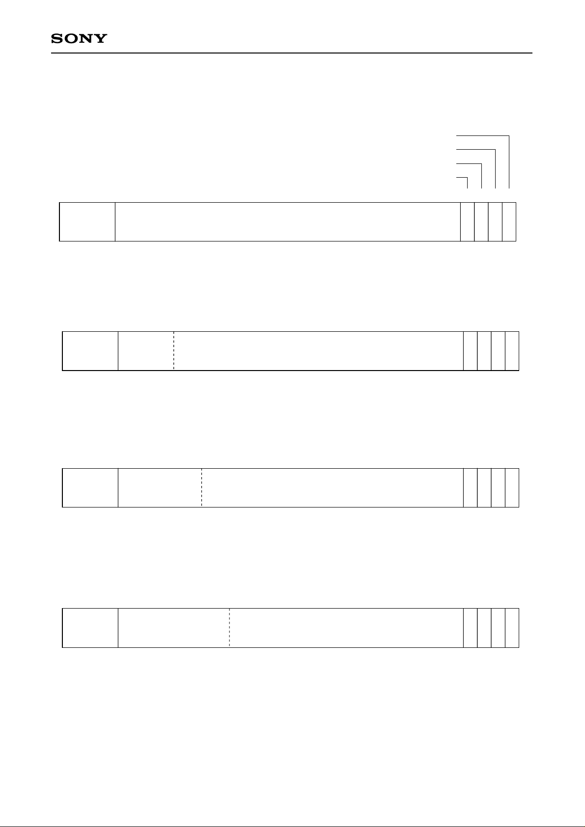
Digital Audio Interface Output Formats
1) 24 bits/word
CXD1852Q
Parity
Channel status
User data
Validity flag
034
Sync
preamble
LSB
2) 20 bits/word
034
Sync
preamble
(0) data
3) 18 bits/word
034
78
LSB
910
28 29 30 31
MSB27VUCP
28 29 30 31
MSB27VUCP
28 29 30 31
Sync
preamble
4) 16 bits/word
034
Sync
preamble
(0) data
(0) data
LSB
11 12
LSB
Data word length setting
DOL1, 0 = 11: 24 bits
DOL1, 0 = 10: 20 bits
DOL1, 0 = 01: 18 bits
DOL1, 0 = 00: 16 bits
MSB27VUCP
28 29 30 31
MSB27VUCP
– 29 –
Page 30
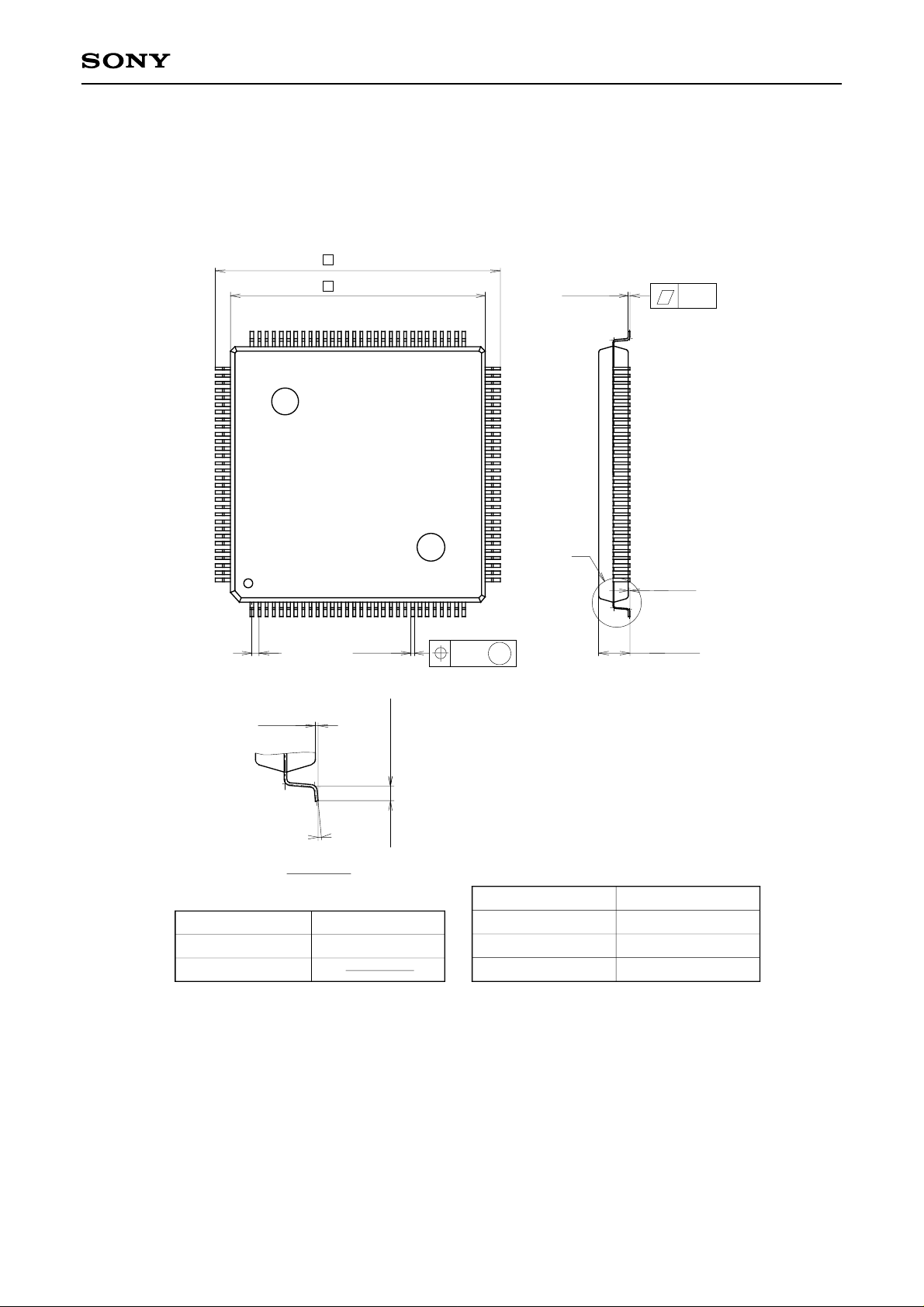
Package Outline Unit: mm
CXD1852Q
120PIN QFP (PLASTIC)
91
120
0.8
31.2 ± 0.2
28.0 ± 0.2
0.35 ± 0.1
6190
301
0.16
+ 0.1
0.15 – 0.05
0.1
60
A
31
M
0.15 ± 0.1
3.45 ± 0.25
SONY CODE
EIAJ CODE
JEDEC CODE
0.15 ± 0.1
0° to 10°
DETAIL
(29.6)
0.8 ± 0.2
A
QFP-120P-L01
∗QFP120-P-2828-A
PACKAGE STRUCTURE
PACKAGE MATERIAL
LEAD TREATMENT
LEAD MATERIAL
PACKAGE WEIGHT
EPOXY RESIN
SOLDER PLATING
COPPER / 42 ALLOY
4.9g
– 30 –
 Loading...