

Page 1

CXD1803AQ/AR
For the availability of this product, please contact the sales office.
CD-ROM DECODER
Description
CXD1803AQ/AR is a CD-ROM decoder LSI with a
built-in ADPCM decoder.
Features
• Compatible with CD-ROM, CD-I and CD-ROM XA
formats
• Real time error correction
• Capable of handling up to quadruple speed
playback
• Connectable with standard SRAM of up to 2M-bit
(256K-byte)
• Connectable with standard DRAM of up to 2M-bit
(256K-byte)
(2 DRAM's of 256K × 4)
• All audio output sampling frequencies: 132.3 KHz
(built-in oversampling filter)
• De-emphasis digital filter
• Digital attenuator
• Connectable directly with Sony's SCSI controller
CXD1185CQ.
CXD1803AQ CXD1803AR
100 pin QFP (Plastic) 100 pin LQFP (Plastic)
Absolute Maximum Ratings (Ta=25°C)
• Supply voltage VDD –0.5 to +7.0 V
• Input voltage VI –0.5 to VDD +0.5 V
• Output voltage VI –0.5 to VDD +0.5 V
• Operating temperature Topr –20 to +75 °C
• Storage temperature Tstg –55 to +150 °C
Recommended Operating Conditions
• Supply voltage VDD
+3.5 to +5.5 (+5.0 typ.) V
• Operating temperature Topr –20 to +75 °C
Applications
CD-ROM drives
Structure
Silicon gate CMOS IC
Sony reserves the right to change products and specifications without prior notice. This information does not convey any license by
any implication or otherwise under any patents or other right. Application circuits shown, if any, are typical examples illustrating the
operation of the devices. Sony cannot assume responsibility for any problems arising out of the use of these circuits.
—1—
E94Y31-TE
Page 2
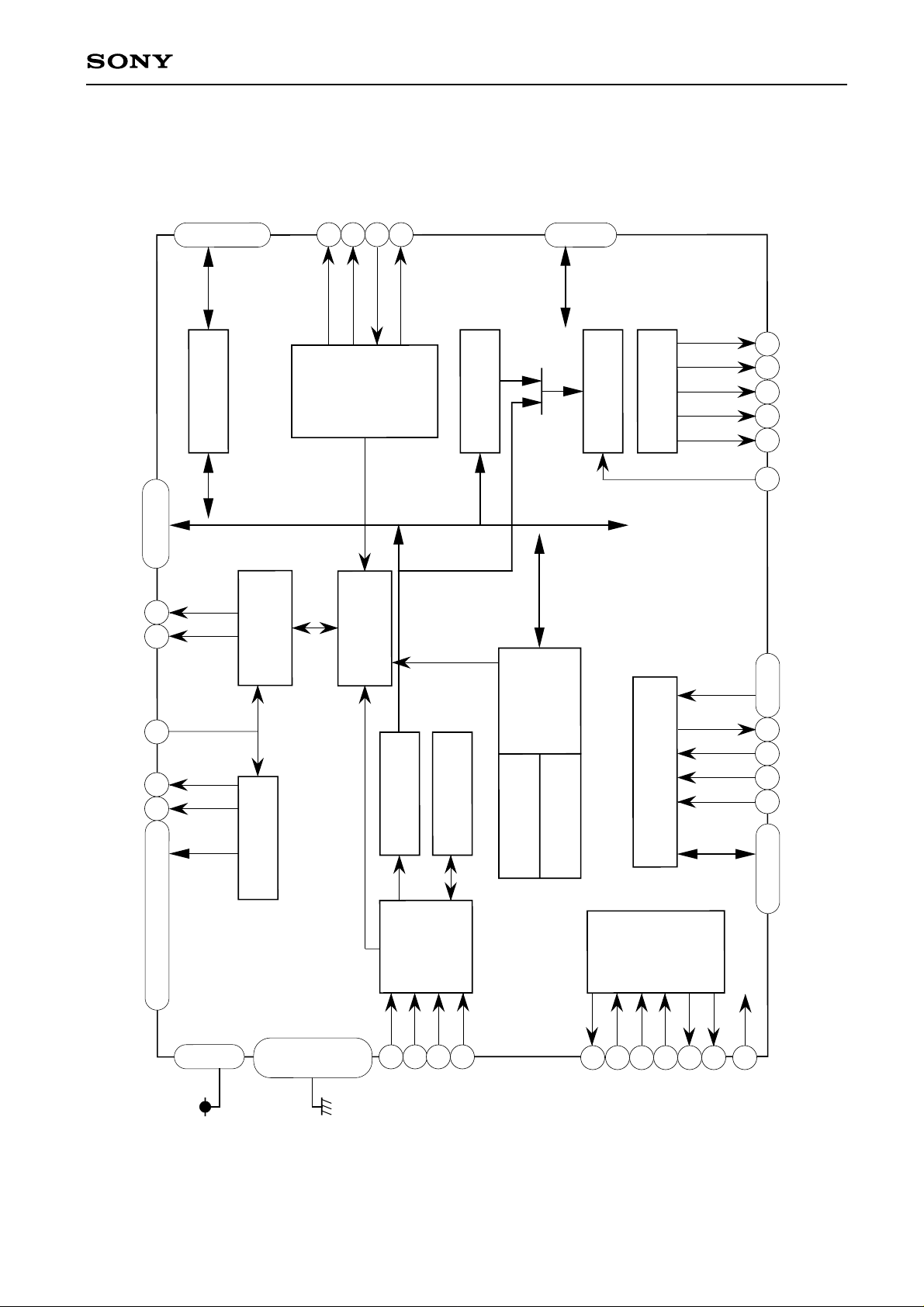
SD0-7
26
27
DMA FIFO
30
CXD1803AQ/AR
XSRD
XSWR
SDRQ
XSAC
|
34
36
24
37
25
HOST I/F
38
ADPCM DECODER
23
TD0-5
96
|
100
DAC I/F
DIGITAL FILETER
95
94
93
92
91
88
MUTE
BCKO
WCKO
LRCO
EMP DATO
MDB0-7,P
XMWR
XMOE
DRAM
XME1
XME0
MA0-16
66—70,72—75
64
63
21
62
57
DMA
SEQUENCER
ADDRESS GEN
PRIORITY
RESOLVER
DESCRAMBLER
SYNC CONTROL
CDP I/F
ECC
CORRECTOR
GALOIS FIELD
SYNDROME GEN
C
L G
Sub CPU I/F
O E
C N
K
A0-A4
17–20,22
16
XINT
14
XWR
13
XRD
12
XCS
D0-7
1,2,5–8,10,11
39,41—46,48—52,55,56,58,59,61
3
Block Diagram
28
53
VDD
78
4, 9
15,21
29,35
40,47
54,60
GND
65,71
79,90
84
LRCK
85
DATA
86
BCLK
—2—
87
C2PO
76
XTL2
77
XTL1
82
CKSL
83
RMCK
CLK
80
81
HCLK
89
XRST
The pin numbers in the diagram are for the CXD1803AQ.
Page 3

Pin Description
CXD1803AQ/AR
Pin No.
QR
1 99 D0 I/O Sub CPU data bus
2 100 D1 I/O Sub CPU data bus
31 VDD — Power supply (+5 V)
4 2 GND — Ground
5 3 D2 I/O Sub CPU data bus
6 4 D3 I/O Sub CPU data bus
7 5 D4 I/O Sub CPU data bus
8 6 D5 I/O Sub CPU data bus
9 7 GND — Ground
10 8 D6 I/O Sub CPU data bus
11 9 D7 I/O Sub CPU data bus
12 10 XCS I IC select negative logic signal from sub CPU
13 11 XRD I Strobe negative logic signal to read this IC internal register from sub CPU
14 12 XWR I Strobe negative logic signal to write this IC internal register from sub CPU
15 13 GND — Ground
16 14 XINT O Interrupt request negative logic signal from IC to sub CPU
17 15 A0 I Sub CPU address
18 16 A1 I Sub CPU address
19 17 A2 I Sub CPU address
20 18 A3 I Sub CPU address
21 19 DRAM I Memory type selection signal. High: DRAM, Low: SRAM
22 20 A4 I Sub CPU address
23 21 TD0 I/O Test input/output
24 22 XSRD O Strobe negative logic signal to read SCSI controller internal register
25 23 XSWR O Strobe negative logic signal to write SCSI controller internal register
26 24 SD0 I/O SCSI controller data bus
27 25 SD1 I/O SCSI controller data bus
28 26 VDD — Power supply (+5 V)
29 27 GND — Ground
30 28 SD2 I/O SCSI controller data bus
31 29 SD3 I/O SCSI controller data bus
32 30 SD4 I/O SCSI controller data bus
33 31 SD5 I/O SCSI controller data bus
34 32 SD6 I/O SCSI controller data bus
Symbol I/O Description
—3—
Page 4

CXD1803AQ/AR
Pin No.
QR
35 33 GND — Ground
36 34 SD7 I/O SCSI controller data bus
37 35 SDRQ I SCSI data request positive logic signal
38 36 XSAC O SCSI acknowledge negative logic signal
39 37 MA0 O Buffer memory address (LSB)
40 38 GND — Ground
41 39 MA1 O Buffer memory address
42 40 MA2 O Buffer memory address
43 41 MA3 O Buffer memory address
44 42 MA4 O Buffer memory address
45 43 MA5 O Buffer memory address
46 44 MA6 O Buffer memory address
47 45 GND — Ground
48 46 MA7 O Buffer memory address
49 47 MA8 O Buffer memory address
50 48 MA9 O Buffer memory address
51 49 MA10 O Buffer memory address
52 50 MA11 O Buffer memory address
53 51 VDD — Power supply (+5 V)
54 52 GND — Ground
55 53 MA12 O Buffer memory address
56 54 MA13 O Buffer memory address
57 55 XME0 O Memory chip enable negative logic signal
58 56 MA14 O Buffer memory address
59 57 MA15 O Buffer memory address
60 58 GND — Ground
61 59
62 60 XME1 O Memory chip enable negative logic signal
63 61
64 62 XMWR O Buffer memory write enable negative logic signal
65 63 GND — Ground
66 64 MDB0 I/O Buffer memory data bus
67 65 MDB1 I/O Buffer memory data bus
Symbol I/O Description
MA16
XRAS DRAM RAS signal
XMOE
XCAS DRAM CAS signal
Buffer memory address
O
Buffer memory output enable negative logic signal
O
—4—
Page 5
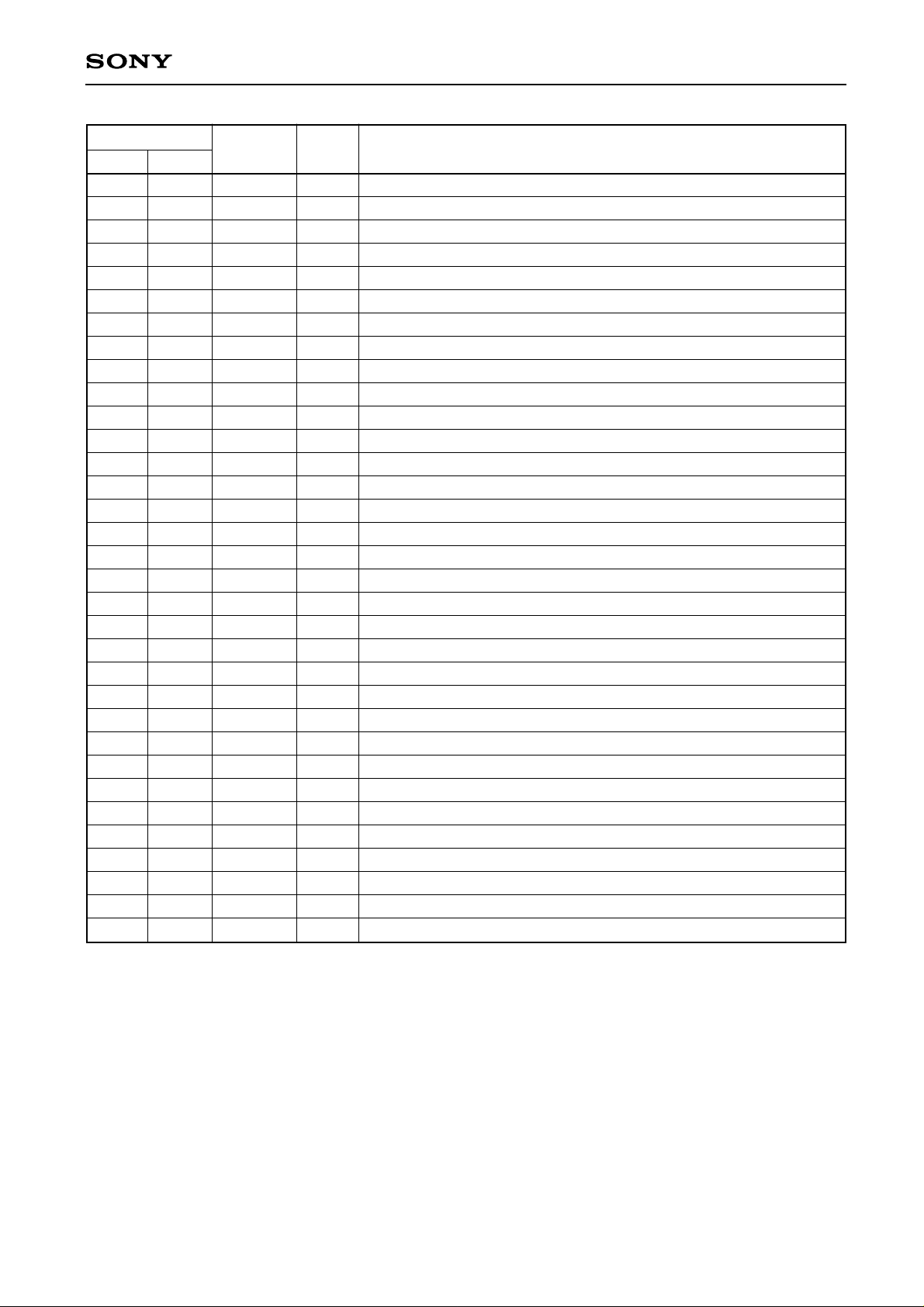
CXD1803AQ/AR
Pin No.
QR
68 66 MDB2 I/O Buffer memory data bus
69 67 MDB3 I/O Buffer memory data bus
70 68 MDB4 I/O Buffer memory data bus
71 69 GND — Ground
72 70 MDB5 I/O Buffer memory data bus
73 71 MDB6 I/O Buffer memory data bus
74 72 MDB7 I/O Buffer memory data bus
75 73 MDBP I/O Buffer memory data bus (for error flag)
76 74 XTL2 O Crystal oscillation circuit output
77 75 XTL1 I Crystal oscillation circuit input (16.9344 MHz)
78 76 VDD — Power supply (+5 V)
79 77 GND — Ground
80 78 CLK O 16.9344 MHz clock output
81 79 HCLK O 8.4672 MHz clock output
82 80 CKSL I Clock select signal for CD-ROM decoder
83 81 RMCK I Clock signal for CD-ROM decoder
84 82 LRCK I LR clock signal from CD DSP (for discriminating L, R channels )
85 83 DATA I Data signal from CD DSP
86 84 BCLK I DATA pin strobe clock signal (bit clock)
87 85 C2PO I Error flag (C2 pointer) positive logic signal from CD DSP
88 86 EMP I Emphasis on positive logic signal from CD DSP
89 87 XRST I Reset negative logic signal
90 88 GND — Ground
91 89 DATO O Data signal to DAC (D/A converter)
92 90 LRCO O LR clock signal to DAC
93 91 WCKO O Word lock signal to DAC
94 92 BCKO O Bit clock signal to DAC
95 93 MUTE O Mute positive logic signal
96 94 TD5 I/O Test input/output
97 95 TD4 I/O Test input/output
98 96 TD3 I/O Test input/output
99 97 TD2 I/O Test input/output
100 98 TD1 I/O Test input/output
Symbol I/O Description
Note: The pin numbers in the column "Q" are for the CXD1803AQ, and those in the column "R" are for the
CXD1803AR.
—5—
Page 6
CXD1803AQ/AR
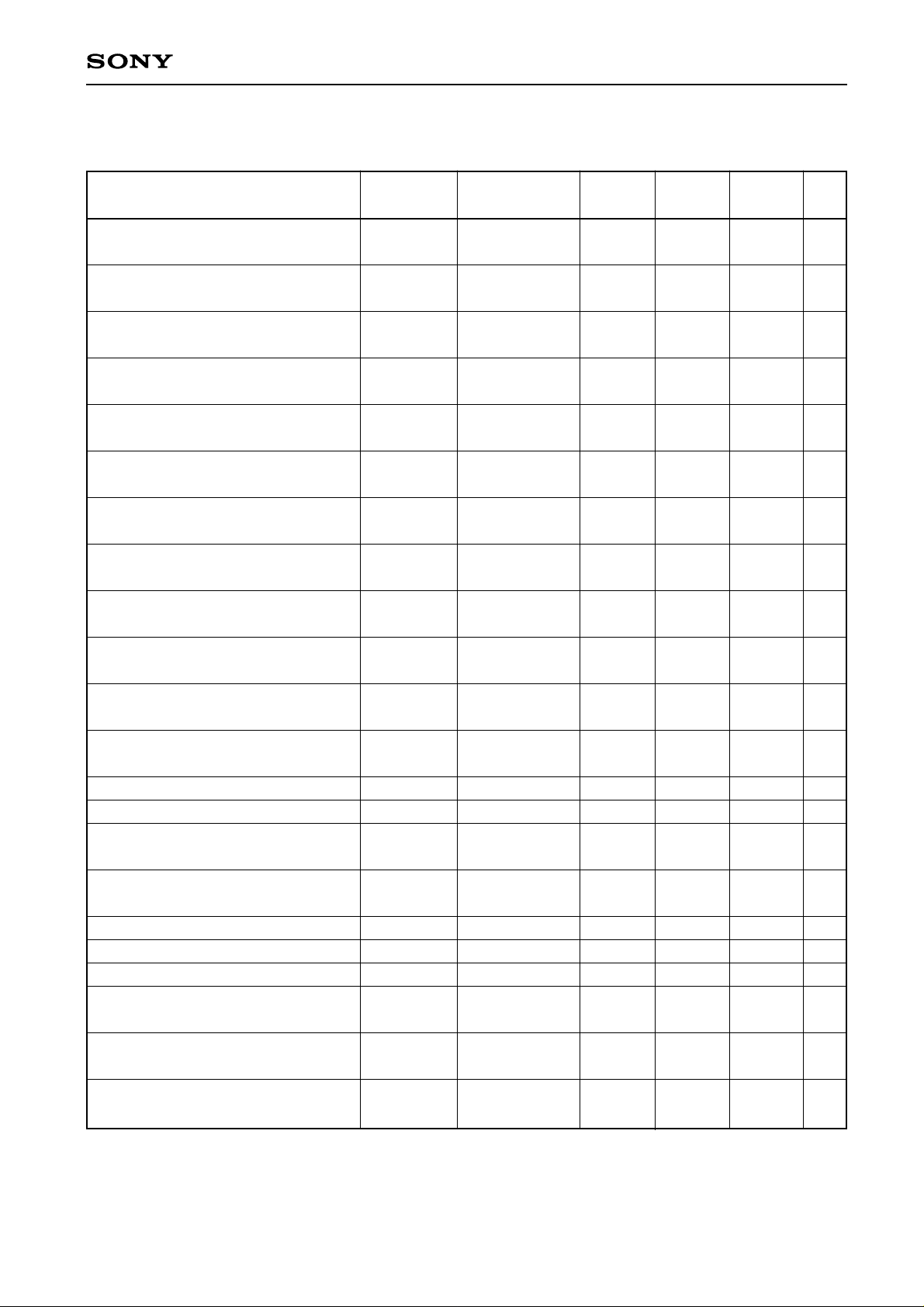
Electrical Characteristics
DC Characteristics (VDD = 5 V ± 10%, VSS = 0 V, Topr = –20 - 75°C)
Item Symbol Conditions Min. Typ. Max. Unit
TTL input level pin ∗1
High level input voltage
TTL input level pin ∗1
Low level input voltage
CMOS input level pin ∗2
High level input voltage
CMOS input level pin ∗2
Low level input voltage
CMOS Schmitt input level pin ∗3
High level input voltage
CMOS Schmitt input level pin ∗3
Low level input voltage
CMOS Schmitt input level pin ∗3
Input voltage hysteresis
TTL Schmitt input level pin ∗4
High level input voltage
TTL Schmitt input level pin ∗4
Low level input voltage
TTL Schmitt input level pin ∗4
Input voltage hysteresis
Bidirectional pin with pull-up resistor ∗5
Input current
Pin with pull-up resistor ∗6
Input current
IH1 2.2 V
V
IL1 0.8 V
V
IH2 0.7VDD V
V
IL2 0.3VDD V
V
IH4 0.8VDD V
V
IL4 0.2VDD V
V
IH4 to VIL4 0.6 V
V
IH5 2.2V V
V
IL5 0.8V V
V
IH4 to VIL4 0.4 V
V
IL3 VIN=0V –90 –200 –440 µA
I
IL4 VIN=0V –40 –100 –240 µA
I
High level output voltage ∗7 VOH1 IOH=–2mA VDD-0.8 V
Low level output voltage ∗7 V
Input leakage current ∗8II1
Output leakage current ∗9IOZ
Oscillation cell ∗10 high level input voltage V
Oscillation cell low level input voltage V
Oscillation cell logic threshold value LV
Oscillation cell feedback resistance value RFB
Oscillation cell
High level output voltage
Oscillation cell
Low level output voltage
OL1 IOL=–4mA 0.4 V
VIN=VSS
or V
DD
High-impedance
state
IH4 0.7VDD V
IL4 0.3VDD V
TH 0.5VDD V
VIN=VSS
or V
DD
OH2 IOH=–3mA 0.5VDD V
V
OL2 IOL=3mA 0.5VDD V
V
–10 10 µA
–40 40 µA
250K 1M 2.5M Ω
—6—
Page 7
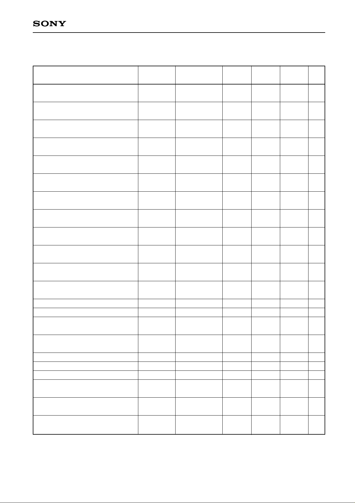
DC Characteristics
Item Symbol Conditions Min. Typ. Max. Unit
CXD1803AQ/AR
(VDD = 3.5 V, VSS = 0 V, Topr = –20 - 75°C)
TTL input level pin ∗1
High level input voltage
TTL input level pin ∗1
Low level input voltage
CMOS input level pin ∗2
High level input voltage
CMOS input level pin ∗2
Low level input voltage
CMOS Schmitt input level pin ∗3
High level input voltage
CMOS Schmitt input level pin ∗3
Low level input voltage
CMOS Schmitt input level pin ∗3
Input voltage hysteresis
TTL Schmitt input level pin ∗4
High level input voltage
TTL Schmitt input level pin ∗4
Low level input voltage
TTL Schmitt input level pin ∗4
Input voltage hysteresis
Bidirectional pin with pull-up resistor ∗5
Input current
Pin with pull-up resistor ∗6
Input current
IH1 2.2 V
V
IL1 0.6 V
V
IH2 0.7VDD V
V
IL2 0.3VDD V
V
IH4 0.8VDD V
V
IL4 0.2VDD V
V
IH4 to VIL4 0.5 V
V
IH5 2.2V V
V
IL5 0.6V V
V
IH5 to VIL4 0.3 V
V
IL3 VIN=0V –20 –50 –110 µA
I
IL4 VIN=0V –10 –25 –60 µA
I
High level output voltage ∗7VOH1 IOH=–1.6mA VDD-0.8 V
Low level output voltage ∗7V
Input leakage current ∗8 II1
Output leakage current ∗9IOZ
Oscillation cell ∗10 high level input voltage V
Oscillation cell low level input voltage V
Oscillation cell logic threshold value LV
Oscillation cell feedback resistance value RFB
Oscillation cell
High level output voltage
Oscillation cell
Low level output voltage
OL1 IOL=3.2mA 0.4 V
VIN=VSS
or V
DD
High-impedance
state
IH4 0.7VDD V
IL4 0.3VDD V
TH 0.5VDD V
VIN=VSS
or V
DD
OH2 IOH=–1.3mA 0.5VDD V
V
OL2 IOL=1.3mA 0.5VDD V
V
–10 10 µA
–40 40 µA
1.2M 2.5M 5M Ω
—7—
Page 8
CXD1803AQ/AR
∗
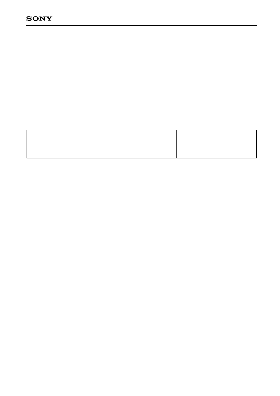
1. D7 to 0, A4 to 0, XWR, XRD, XCS, MDB7 to 0, MDBP, SD7 to 0, TD7 to 0
∗
2. DATA, LRCK, C2PO, EMP, CKSL, RMCK
∗
3. BCLK, XRST
∗
4. A4 to 0, XWR, XRD, XCS, SDRQ
∗
5. D7 to 0, MDB7 to 0, MDBP, SD7 to 0, TD7 to 0
∗
6. CKSL
∗
7. All output pins except XTL2
∗
8. All input pins except ∗5, ∗6, and XTL1
∗
9. HINT
∗
10. Input: XTL1, Output: XTL2
I/O Capacitance
(VDD = VI = 0 V, f = 1 MHz)
Item Symbol Min. Typ. Max. Unit
Input pin CIN 9pF
Output pin COUT 11 pF
I/O pin COUT 11 pF
—8—
Page 9
CXD1803AQ/AR
AC Characteristics (VDD = 5 V±10%, VSS = 0 V, Topr = –20 to 75°C, output load = 50 pF)
The values in parentheses on the tables for VDD = 3.5 V, VSS = 0 V, Topr = –20 to 75°C, output load = 50 pF.
Those without parentheses for VDD = 5 V±10% and 3.5 V.
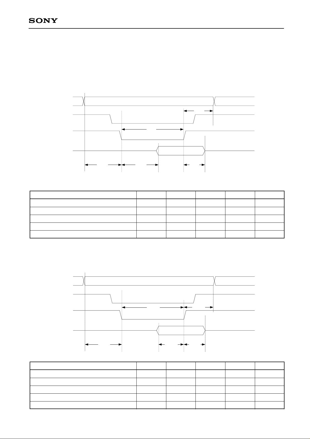
1. Sub CPU Interface
(1) Read
A0
Thar
XCS
Trrl
XRD
D7-0
Tsar
Tdrd
Tfrd
Item Symbol Min. Typ. Max. Unit
Address setup time (for XCS & XRD ↓) Tsar 30 (70) ns
Address hold time (for XCS & XRD ↑) Thar 20 (50) ns
Data delay time (for XCS & XRD↓) Tdrd 60 (100) ns
Data float time (for XCS & XRD ↑) Tfrd 0 15 (25) ns
Low level XRD pulse width Trrl 100 (150) ns
Note) "&" indicates "AND".
(2) Write
A0
XCS
Twwl
XWR
Thaw
D7-0
Tsaw
Tsdw
Thdw
Item Symbol Min. Typ. Max. Unit
Address setup time (for XCS & XWR ↓) Tsaw 30 (70) ns
Address hold time (for XCS & XWR ↑) Thaw 20 (50) ns
Data setup time (for XCS & XWR ↓) Tsdw 40 (70) ns
Data hold time (for XCS & XWR ↑) Thdw 10 (30) ns
Low level XWR pulse width Twwl 50 (80) ns
—9—
Page 10

2. CD DSP Interface
BCKRED='H'
BCLK
DATA
LRCK
Tbck
Tsb1 Thb1
CXD1803AQ/AR
Tbck
C2PO
BCKRED='L'
BCLK
DATA
LRCK
C2PO
Tbck
Tsb1 Thb1
Thb2
Tbck
Thb2
Tsb2
Tsb2
Item Symbol Min. Typ. Max. Unit
BCLK frequency Fbck 11.3 MHz
BCLK pulse width Tbck 88 ns
DATA setup time (for BCLK) Tsb1 20 ns
DATA hold time (for BCLK) Thb1 20 ns
LRCK, C2PO setup time (for BCLK) Tsb2 20 ns
LRCK, C2PO hold time (for BCLK) Thb2 20 ns
—10—
Page 11
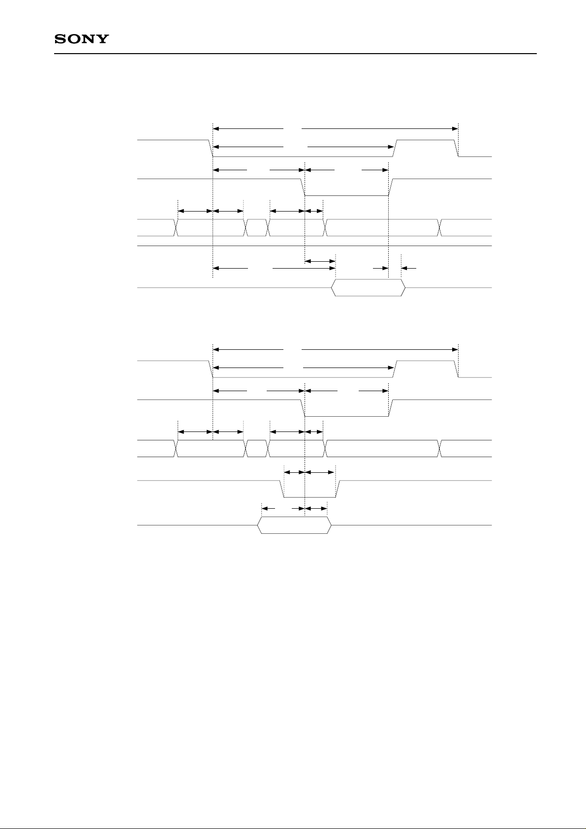
3. DRAM Interface
(1) Read
CXD1803AQ/AR
Trc
XRAS
XCAS
MA9-0
XMWR
MDB7-0, P
(2) Write
XRAS
XCAS
Tras
Trcd Tcas
Tasr
Tasr Trah Tasc Tcah
Trah Tasc Tcah
Row Column
Tcdd
Trdd
Trc
Tras
Trcd Tcas
Tcdh
'H'
MA9-0
XMWR
MDB7-0, P
Row Column
Twcs Twch
Tds
Tdh
—11—
Page 12
CXD1803AQ/AR
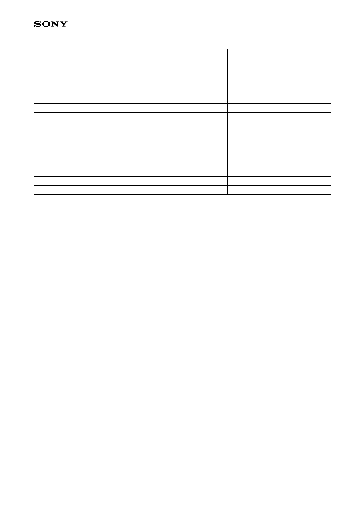
Item Symbol Min. Typ. Max. Unit
Random read/write cycle time Trc 4Tw ns
RAS pulse width Tras 2Tw ns
RAS CAS delay time Trcd Tw ns
CAS pulse width Tcas Tw ns
Row address setup time Tasr 10 ns
Row address hold time Trah 20 ns
Column address setup time Tasc 0 ns
Column address hold time Tcah 20 ns
Delay time from RAS Trdd 2Tw-20 ns
Delay time from CAS Tcdd Tw-20 ns
Hold time from CAS Tcdh 0 ns
Write command setup time Twcs 10 ns
Write command hold time Twcs 20 ns
Data output setup time Tds Tw ns
Data output hold time Tds Tw ns
—12—
Page 13
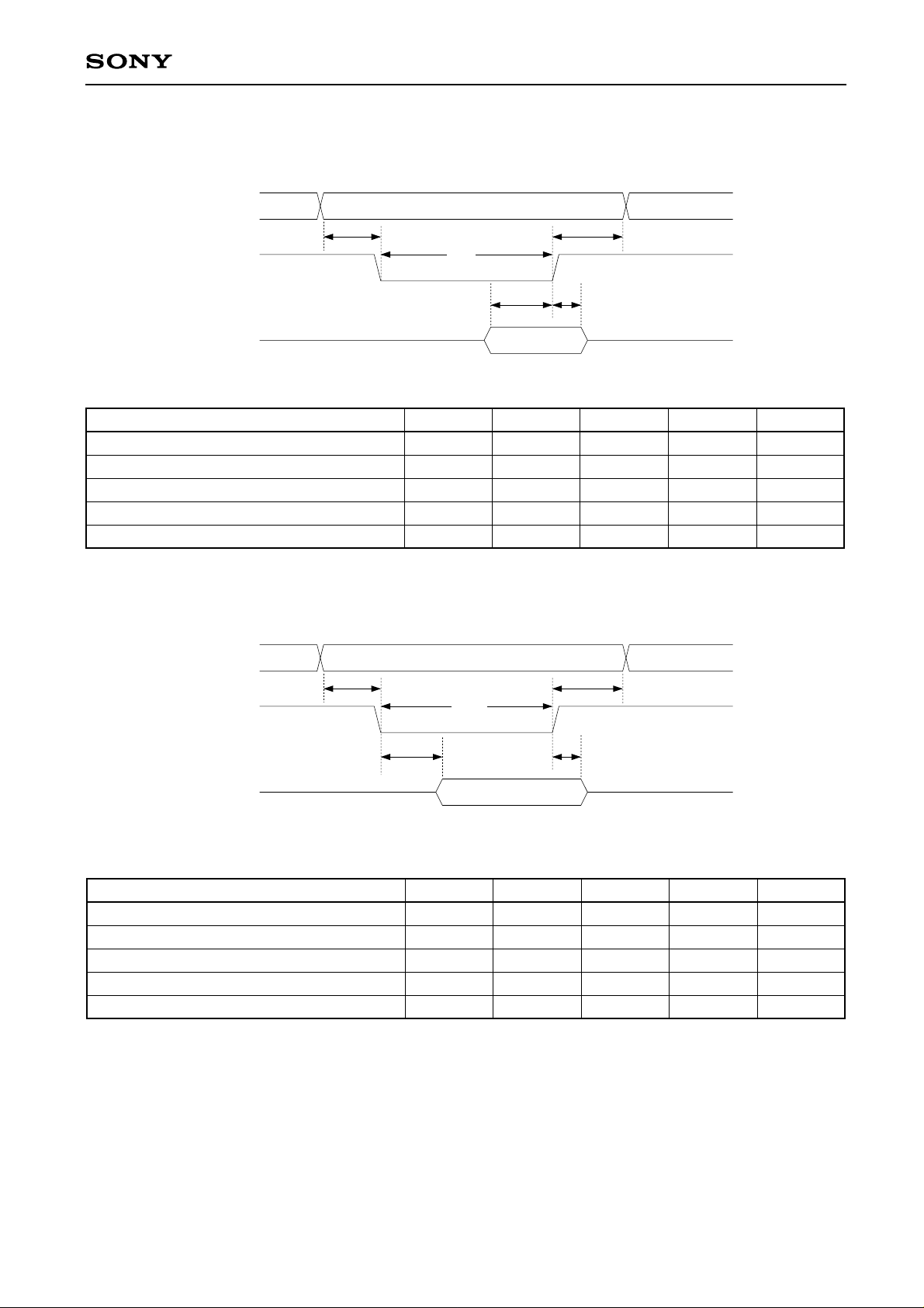
4. SRAM Interface
(1) Read
MA16-0
CXD1803AQ/AR
XMOE
MDB7-0,P
Taso
Trrl
Tsdo Thod
Thoa
XMWR='H'
Item Symbol Min. Typ. Max. Unit
Address setup time (for XMOE ↓) Tsao Tw-30 ns
Address hold time (for XMOE ↑) Thoa Tw-10 ns
Data setup time (for XMOE ↑) Tsdo 50 (100) ns
Data hold time (for XMOE ↑) Thod 10 (20) ns
Low level XMOE pulse width Trrl 2Tw ns
(2) Write
MA16-0
XMWR
MDB7-0,P
Tsaw
Twwl
Tdwd Tfwd
Thwa
XMOE='H'
Item Symbol Min. Typ. Max. Unit
Address setup time (for XMWR ↓) Tsaw Tw-30 ns
Address hold time (for XMWR ↑) Thwa Tw-10 ns
Data delay time (for XMWR ↓) Tdwd 10 ns
Data float time (for XMWR ↑) Tfwd 10 ns
Low level XMMR pulse width Twwl 2Tw ns
—13—
Page 14
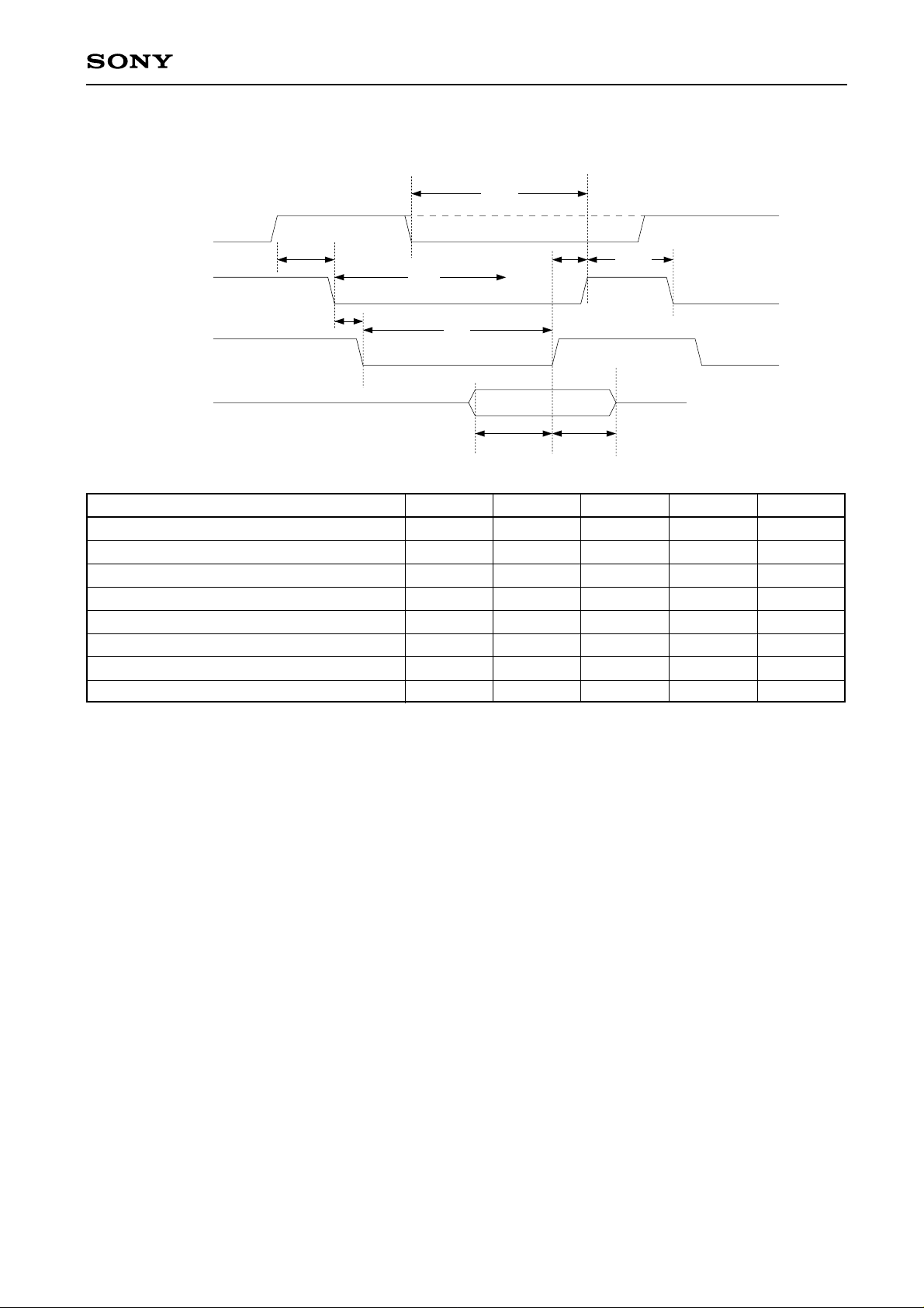
5. SCSI Controller Interface
(1) Read
SDRQ
CXD1803AQ/AR
Tsdq
XSAC
XSRD
SD7 to 0
Tdaw
Tdda
Tdar
Twwl
Trrl
Tsdr Thdr
Tasc
Item Symbol Min. Typ. Max. Unit
XSAC fall time (for SDRQ ↑) Tdda 5×Tw ns
XSRD delay time (for XSAC ↓) Tdaw 0 ns
XSAC delay time (for XSRD ↑) Tdar Tw ns
Data setup time (for XSRD ↓) Tsdr 20 (60) ns
Data hold time (for XSRD ↑) Thdr 10 (30) ns
Low level XSRD pulse width Trrl T1 ns
SDRQ setup time (for XSAC ↑) Tsdq 15 (30) ns
XSAC fall time (for XSAC ↑) Tsac Tw ns
—14—
Page 15

(2) Write
SDRQ
CXD1803AQ/AR
Tsdq
XSAC
XSWR
SD7 to 0
Tdda
Tdaw
Twwl
Tsdr
Tdwa
Thdr
Tsac
Item Symbol Min. Typ. Max. Unit
XSAC fall time (for SDRQ ↑) Tdda 5×Tw ns
XSWR delay time (for XSAC ↓) Tdaw Tw ns
XSAC delay time (for XSWR ↑) Tdwa Tw ns
Data setup time (for XSWR ↑) Tsdr 2×Tw-30 ns
Data hold time (for XSWR ↑) Thdr Tw-10 ns
Low level XSWR pulse width Twwl T2 ns
SDRQ setup time (for XSAC ↑) Tsdq 15 (30) ns
XSAC fall time (for XSAC ↑) Tsac Tw ns
Here:
2×Tw: 3cyclemode
T1=3×Tw: 4cyclemode
4×Tw: 5cyclemode
Tw: 3cyclemode
T2=2×Tw: 4cyclemode
3×Tw: 5cyclemode
Tw is the CD-ROM decoder clock cycle.
—15—
Page 16
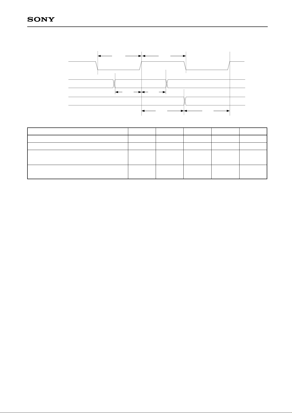
6. DAC Interface
CXD1803AQ/AR
Tbco
BCKO
DATO
Tsbo Thbo
WCKO
LRCO
Tbco
Thbo
Tsbo
Item Symbol Min. Typ. Max. Unit
BCKO frequency Fbco 8.4672 MHz
BCKO pulse width Tbco 50 ns
DATO, WCO1, WCO2, LRCO setup time
(for BCKO ↑)
DATO, WCO1, WCO2, LRCO hold time
(for BCKO ↑)
Tsbo 30 ns
Thbo 30 ns
—16—
Page 17
CXD1803AQ/AR
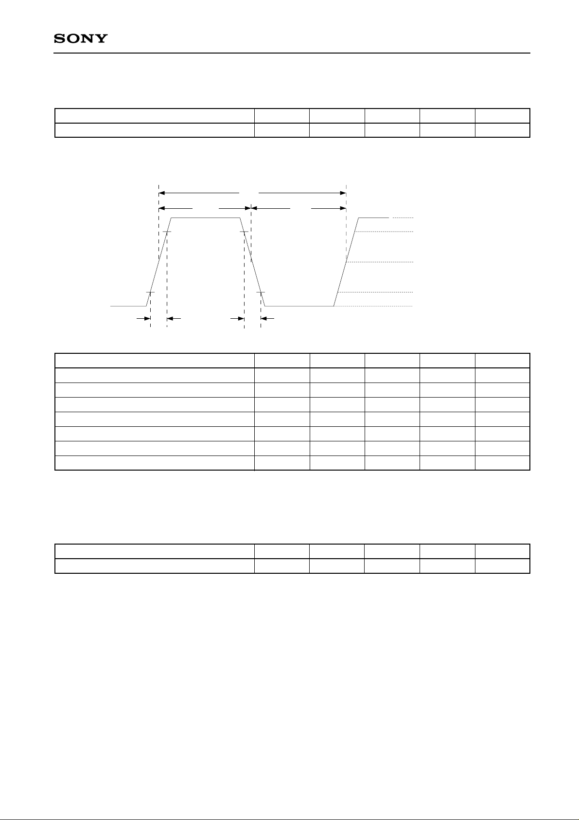
7. XTL1 and XTL2 Pins
(1) For self-excited oscillation
Item Symbol Min. Typ. Max. Unit
Oscillation frequency Fmax 16.9344 MHz
(2) When a pulse is input to XTL1 pin
Tw
Tr
Twhx
Tf
Twlx
Vihx
Vihx∗0.9
Vdd/2
Vilx∗2
Vilx
Item Symbol Min. Typ. Max. Unit
High level pulse width Twhx 20 ns
Low level pulse width Twlx 20 ns
Pulse cycle Tw 59 ns
Input high level Vihx VDD-1.0 ns
Input low level Vilx 0.8 ns
Rise time Tr 15 ns
Fall time Tf 15 ns
Note: Synchronize the XTL1 clock signal with that of the CD DSP. (Use the clock signal from the
same oscillator.)
8. RMCK Pin
Item Symbol Min. Typ. Max. Unit
Frequency frmck 33.3 (23.4) MHz
Note: The maximum RMCK frequency is 35.0 MHz, when VDD = 5 V ±5%, Playback at quadruple
normal speed can be accommodated when a clock signal with a frequency double 16.9344
MHz or more is input to RMCK.
—17—
Page 18

CXD1803AQ/AR
Description of Functions
1. Pin Description
The pin description by function is given below.
1.1.CD player interface (5 pins)
This enables direct connection with the digital signal processor LSI for Sony's CD players. Digital signal
processor LSI for CD applications are hereafter called "CD DSP". See 2-1-1 for the data formats.
(1) DATA (DATA: input)
Serial data stream from CD DSP.
(2) BCLK (bit clock: input)
Bit clock signal; data signal strobe.
(3) LRCK (LR clock: input)
LR clock signal; indicates left and right channels of DATA signals.
(4) C2PO (C2 pointer: input)
C2 pointer signal; indicates that an error is contained in DATA input.
(5) EMP (emphasis: input)
Emphasis positive logic signal; indicates that emphasis has been applied to data from CD DSP.
1.2.Buffer memory interface (30 pins)
This is connected with a 32K-byte (256K-bit) or 128K-byte (1M-bit) standard SRAM; also connected with
256K-byte standard DRAM (two DRAMs of 128K-byte).
(1) XMWR (buffer memory write: output)
Data write strobe negative logic output signal to buffer memory.
(2) XMOE/XCAS (buffer memory output enable/column address strobe: output)
When connected to SRAM, data read strobe negative logic output signal to buffer memory.
When connected to DRAM, XCAS (column address strobe negative logic) signal.
(3) MA0 to 15 (buffer memory address: output)
Address signals to buffer memory. When connected to DRAM, MA0 to 8 are valid.
(4) MA16/XRAS (buffer memory address/row address strobe: output)
When connected to SRAM, address signal to buffer memory. XRAS (row address strobe negative
logic) signal when connected to DRAM.
(5) XME0, 1 (buffer memory chip enable: output)
When connected to a chip SRAM, chip enable negative logic signal to buffer memory. Not used when
connected to DRAM.
(6) MDB0 to 7, P (buffer memory data bus: bus)
Data bus signals to buffer memory; pulled up by standard 25kΩ resistor; MDBP pin is left open when
connected to an 8-bit/word SRAM.
(7) DRAM (buffer memory DRAM: input)
High is input when DRAM is connected as buffer memory.
Low is input when SRAM is connected as buffer memory.
—18—
Page 19

1.3.Sub CPU interface (17 pins)
(1) XWR (sub CPU write: input)
Strobe negative logic input signal for writing IC internal register.
(2) XRD (sub CPU read: input)
Strobe negative logic input signal for reading IC internal register status.
(3) D0 to 7 (sub CPU data bus: input/output)
8-bit data bus.
(4) A0 to 4 (sub CPU address: input)
Address signal for selecting IC internal register from sub CPU.
(5) XINT (sub CPU interrupt: output)
Interrupt request negative logic signal to sub CPU.
(6) XCS (chip select: input)
IC select negative logic signal from sub CPU.
1.4.SCSI controller interface (13pins)
(1) SDRQ (SCSI data request: input)
DMA data request positive logic signal from SCSI controller IC.
(2) XSAC (SCSI DMA acknowledge: output)
DMA acknowledge negative logic signal to SCSI controller IC.
(3) XSWR (SCSI write: negative logic output)
Data write strobe output to SCSI controller IC.
(4) XSRD (SCSI read: negative logic output)
Data read strobe output to SCSI controller IC.
(5) SD0 to 7 (SCSI controller bus: input/output)
SCSI controller data bus signal.
CXD1803AQ/AR
1.5.DAC interface (4 pins)
The output format to DAC is shown in Fig. 1-1.
(1) BCKO (bit clock output: output)
Bit clock output signal to D/A converter.
(2) WCKO (word clock output: output)
Word clock output signal to D/A converter.
(3) LRCO (LR clock output: output)
LR clock output signal to D/A converter.
(4) DATO (data output: output)
Data output signal to D/A converter.
—19—
Page 20

R CH
CXD1803AQ/AR
49 64
32
MSB
1234 5678910 11 12 13 14 15 16
Fig. 1-1 Output Format to D/A Converter
17
1234
BCKO
MSB L CH LSB
123 45 678910 11 12 13 14 15 16
16
DATO
WCKO
LRCO
—20—
Page 21

1.6.Others (16 pins)
(1) MUTE (mute: output)
Outputs high when DA data (DATO) is muted.
(2) XRST (reset: input)
Chip reset negative logic input signal.
(3) XTL1 (crystal 1: input)
(4) XTL2 (crystal 2: output)
A 16.9344 MHz crystal oscillator is connected between XTL1 and XTL2. (The capacitor value
depends on the crystal oscillator.)
Alternatively, a 16.9344 MHz clock signal is input to the XTL1 pin.
(5) CLK (cock: output)
Outputs a 16.9344 MHz clock signal. The output can be fixed low when this signal is not used.
(6) HCLK (half clock: output)
Outputs an 8.4672 MHz clock. The output can be fixed low when this signal is not used.
(7) CKSL (clock select: input)
High or open: The IC is operated by the XTL1 clock.
Low: The audio block (ADPCM decoder and digital filter) is operated by the XTL1 clock,
and the CD-ROM decoder block is operated by the RMCK clock.
This pin is pulled up by a standard 50kΩ resistor in the IC .
(8) RMCK (ROM clock: input)
When the CKSL pin is set low, the clock of the CD-ROM decoder block is input. When it is high or left
open, fix the RMCK pin high or low.
(9) TD0 to 5 (test data 0 to 5: input/output)
Data pins for testing the IC . They are pulled up by a 25kΩ standard resistor and are normally left
open.
CXD1803AQ/AR
—21—
Page 22
2. Sub CPU Registers
2.1.Write registers
2.1.1. DRVIF (drive interface) register
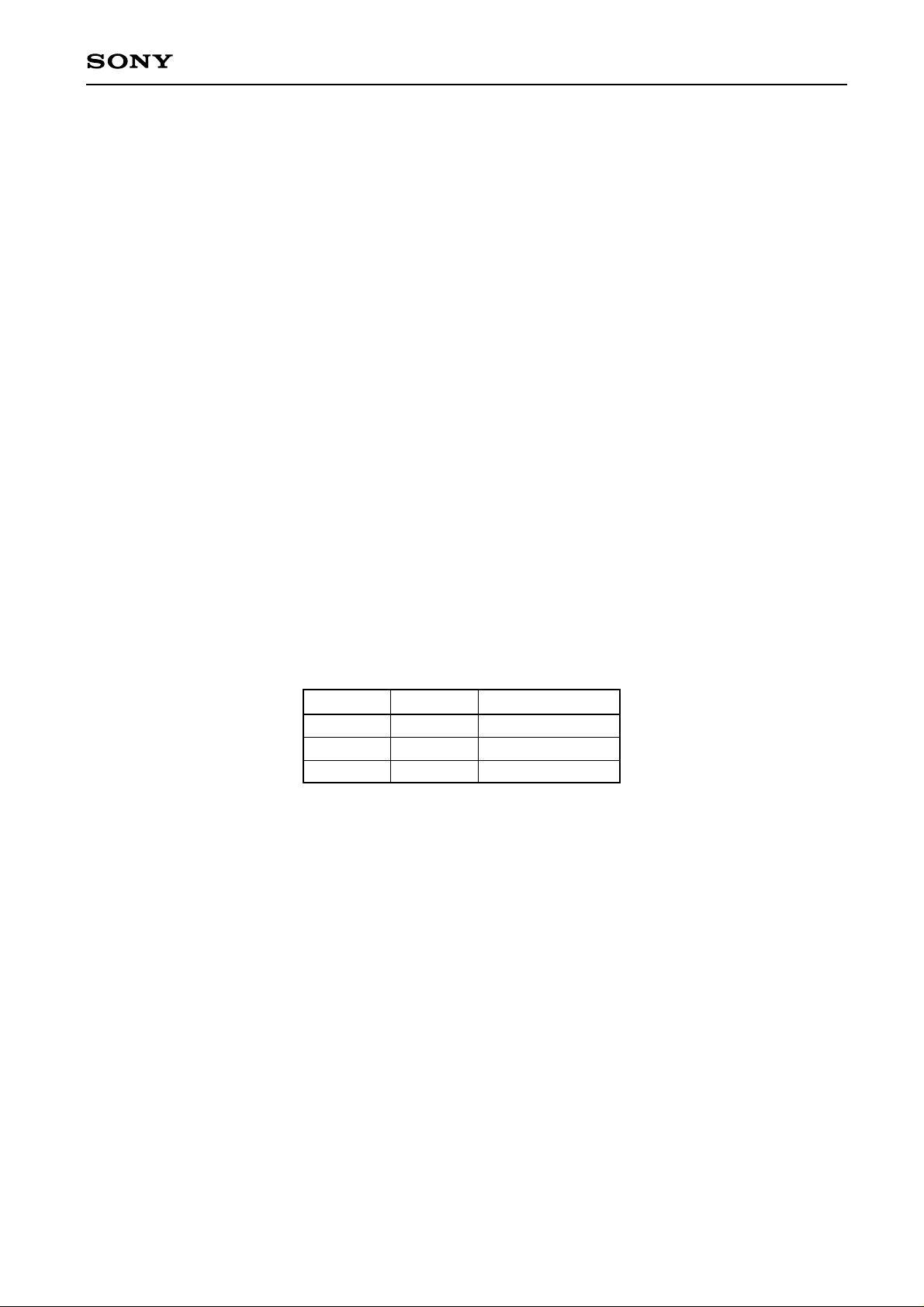
This register controls the connection mode with the CD DSP. After the IC is reset, the sub CPU sets
this register according to the CD DSP to be connected.
bit 7: C2PL1ST (C2PO lower byte first)
High: When two bytes of data are input, C2PO inputs the lower byte first followed by the
upper byte.
Low: When two bytes of data are input, C2PO inputs the upper byte first followed by the
lower byte.
Here, "upper byte" means the upper 8 bits including MSB from the CD DSP and "lower
byte" means the lower 8 bits including LSB from the CD DSP. For example, the
header minute byte is the lower byte and the second byte, the upper byte.
bit 6: LCHLOW (Lch low)
High: When LRCK is low, determined to be the left channel data.
Low: When LRCK is high, determined to be the left channel data.
bit 5: BCKRED (BCLK rising edge)
High: Data is strobed at the rising edge of BCLK.
Low: Data is strobed at the falling edge of BCLK.
bits 4,3: BCKMD1, 0 (BCLK mode1, 0)
These bits are set according to the number of clocks output for BCLK during one WCLK cycle
by the CD digital signal processing LSI (CD DSP).
CXD1803AQ/AR
BCKMD1 BCKMD0
'L' 'L' 16BCLKs/WCLK
'L' 'H' 24BCLKs/WCLK
'H' 'X' 32BCLKs/WCLK
bit 2: LSB1ST (LSB first)
High: Connected with the CD DSP which outputs data with LSB first.
Low: Connected with the CD DSP which outputs data with MSB first.
bits 1,0: Reserved
Normally set low.
Any change of each bit in this register must be made in the decoder disable status. Table 2-1-1
indicates the setting values for bits 7 to 2 when this IC is connected to Sony's CD DSP.
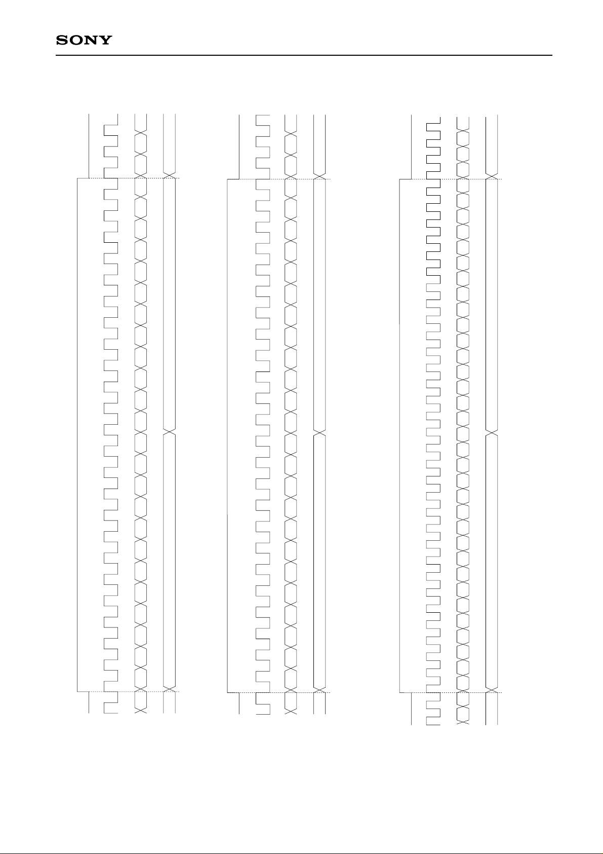
Figs. 2-1-1(1) to (3) are input timing charts.
—22—
Page 23
123
CXD1803AQ/AR
Lch LSB
for Lower Bytefor Upper Byte
Lch LSB
for Lower Bytefor Upper Byte
Rch MSB
31 32
29 3031 32 4
28
27
25 26
R7L14
for Lower Bytefor Upper Byte
R4
R0 R15R14R13R12R11R10R9R8R6R5R3R2R1L15
LRCK
24123456789101112131415161718192021222324123
BCLK
L15 L0L1L2L3L4L5L6L7L8L9L10L11L12L13L14R0
Rch LSB Lch MSB
DATA
L15 L0L1L2L3L4L5L6L7L8L9L10L11L12L13L14R0
Fig. 2-1-1 (1) CDL30 and 35 Series Timing Chart
1 2 3 4 5 6 7 8 9 101112131415161718192021222324
C2PO
LRCK
24
BCLK
Rch LSB Lch MSB
DATA
C2PO
Fig. 2-1-1 (2) CDL40 Series Timing Chart (48-bit slot mode)
1 2 3 4 5 6 7 8 9 101112131415161718192021222324 1 2 3
Fig. 2-1-1 (3) CDL40 Series Timing Chart (64-bit slot mode)
Lch MSB Rch LSB
BCLK
DATA
C2PO
LRCK
—23—
Page 24
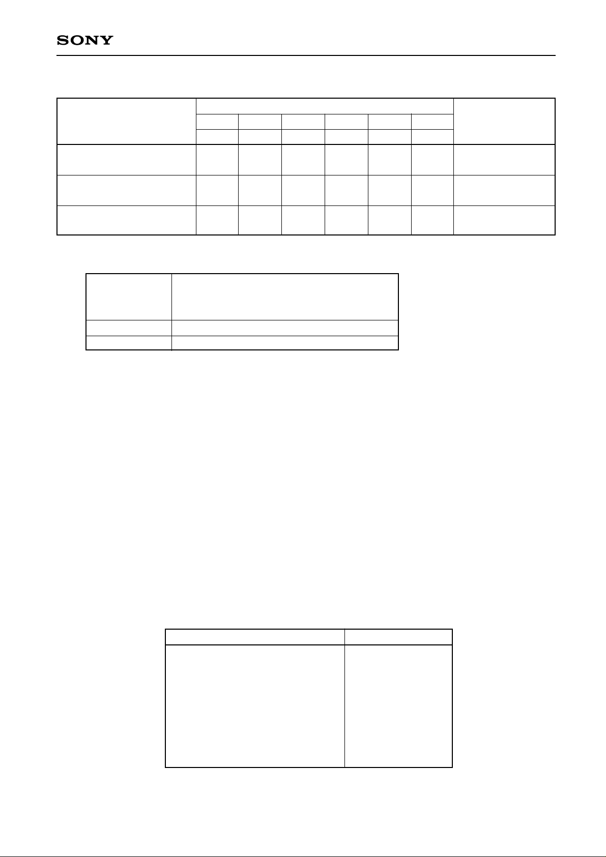
Sony CD DSP bit7 bit6 bit5 bit4 bit3 bit2 Timing chart
CDL30 Series
CDL35 Series
CDL40 Series
(48-bit slot mode)
CDL40 Series
(64-bit slot mode)
Note 1)
CDL30 Series CXD1241Q/QZ, CXD1245Q, CXD1246Q/QZ
CDL35 Series CXD1165Q, CXD1167Q/QZ/R, etc.
CDL40 Series CXD2500Q/QZ, etc.
CXD1803AQ/AR
Table 2-1-1 DRVIF Register Settings
DR VIF register
c2po lrck bedg bck1 bck0 lsb
L L L L H L Fig. 2-1-1(1)
L L H L H L Fig. 2-1-1 (2)
L H L H X H Fig. 2-1-1(3)
CXD1125Q/QZ, CXD1130Q/QZ, CXD1135Q/QZ
CXD1247Q/QZ/R, etc.
2.1.2. CONFIG1 (configuration 1) register
This register is set depending on the IC peripheral hardware. The sub CPU sets this register after the
IC is reset.
bit 7: Reserved
Normally set low.
bit 6: XSLOW
The number of clock signals per DMA1 cycle is determined by this bit.
High: 4 clock signals
Low: 12 clock signals
Set low when a low-speed SRAM is connected for VDD = 3.5 V.
When XSLOW is low, erasure correction and double speed playback are prohibited.
bit 5: Reserved
Normally set low.
bits 4,3: RAMSZ1, 0 (RAM size 1, 0)
bit 2: 9BITRAM
These bits are set depending on the size of the buffer memory connected to the IC.
RAMSZ1 RAMSZ0 9BITRAM Memory size
'L' 'L' 'L' 32KW×8
'L' 'L' 'H' 32KW×9
'L' 'H' 'L' 64KW×8
'L' 'H' 'H' 64KW×9
'H' 'L' 'L' 128KW×8
'H' 'L' 'H' 128KW×9
'H' 'H' 'L' 256KW×8
'H' 'H' 'H' 256KW×9
b
b
b
b
b
b
b
b
Refer to Chapter 3 for information on buffer memory connection.
—24—
Page 25

bit 1: CLKDIS (CLK disable)
High: The CLK pin is fixed low.
Low: A 16.9344 MHz clock signal is output from the CLK pin.
bit 0: HCLKDIS (half CLK disable)
High: The HCLK pin is fixed low.
Low: An 8.4672 MHz clock signal is output from the HCLK pin.
2.1.3. CONFIG2 (configuration 2) register
This register is set depending on the IC peripheral hardware. The sub CPU sets this register after the
IC has been reset.
bits 7, 6:SCYC1, 0 (SCSI DMA cycle 1, 0)
Data transfer between the IC and the SCSI control IC is executed by the following number of
clock signals.
SCYC1 SCYC0
'L' 'L' 3 clock signals
'L' 'H' 4 clock signals
'H' 'X' 5 clock signals
CXD1803AQ/AR
bit 5: SPECTL (sound parameter error control)
bit 4: SPMCTL (sound parameter majority control)
These two bits control the processing of the sound parameters for ADPCM playback.
bit 3: SMBF2 (sound map buffer 2)
Indicates the number of buffer surfaces for the sound map ADPCM.
High: 2 buffer surfaces for the sound map
Low: 3 buffer surfaces for the sound map
bit 2: DAMIXDIS (digital audio mixer disable)
High: Attenuator and mixer are not activated for CD-DA.
Low: Attenuator and mixer are activated for CD-DA.
bit 1: DACOUTEN (DAC out enable)
High: Clock signals are output from the WCKO, LRCO and BCKO pins even for muting.
Low: The WCKO, LRCO and BCKO pins are set low for muting.
bit 0: PRTYCTL (priority control)
When double speed playback with erasure correction is carried out with the CD-ROM decoder
clock frequency at 18 MHz or less, this bit goes high. In this case, priority is given to buffer
access for ECC, and the data transfer rate to the SCSI controller drops.
—25—
Page 26
2.1.4. DECCTL (decoder control) register
bit 7: ENDLADR (enable drive last address)
High: DLADR (drive last address) is enabled when this is set high. When DADRC and
DLADR become equal while the decoder is in the write-only, real-time correction or
CD-DA mode, the data writing from the drive into the buffer is stopped.
Low: DLADR (drive last address) is disabled when this is set low. Even when DADRC and
DLADR become equal while the decoder is in the write-only, real-time correction or
CD-DA mode, the data writing from the drive into the buffer is not stopped.
bit 6: ECCSTR (ECC strategy)
High: Errors are corrected with consideration given to the error flags of the data.
Low: Errors are corrected with no consideration given to the error flags of the data. In this
case, there is no erasure correction. Set this bit low when the IC is connected to an
8-bit/word SRAM.
bit 5: MODESEL (mode select)
bit 4: FORMSEL (form select)
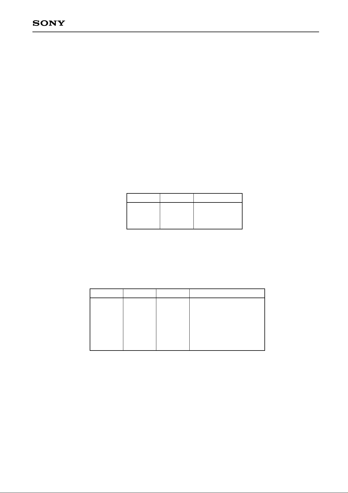
When AUTODIST is low, the sector is corrected in the MODE or FORM indicated below.
CXD1803AQ/AR
MODESEL FORMSEL
'L' 'L' MODE1
'H' 'L' MODE2, FROM1
'H' 'H' MODE2, FROM2
bit 3: AUTODIST (auto distinction)
High: Errors are corrected according to the MODE byte and FORM bit read from the drive.
Low: Errors are corrected according to the MODESEL and FORMSEL bits (bits 5 and 4).
bits 2 to 0:DECMD2 to 0 (decoder mode 2 to 0)
DECMD2 DECMD1 DECMD0
'L' 'L' 'X' Decoder disable
'L' 'H' 'X' Monitor-only mode
'H' 'L' 'L' Write-only mode
'H' 'L' 'H' Real-time correction mode
'H' 'H' 'L' Repeat correction mode
'H' 'H' 'H' CD-DA mode
When the CD-DA bit (bit 4) in the CHPCTL register is to be set high, set the decoder to the disable or
CD-DA mode.
—26—
Page 27

2.1.5. DLADR-L
2.1.6. DLADR-M
2.1.7. DLADR-H
While the decoder is in the write-only, real-time correction or CD-DA mode, the last address is set for
the buffer write data from the drive. When the ENDLADR bit (bit 7) of the DECCTL register is high and
the data from the drive is written into the address assigned by DLADR while the decoder is in any of
the above modes, all subsequent writing in the buffer is prohibited.
2.1.8. CHPCTL (chip control) register
bit 7: SM MUTE (sound map mute)
When this is set high, the audio output is muted for sound map ADPCM playback.
bit 6: RT MUTE (real time mute)
When this is set high, the audio output is muted for real-time ADPCM playback.
bit 5: CD-DA MUTE
When bit 4 is high and this bit is also set high for a CD-DA (digital audio) disc playback, the
audio output is muted. When bit 4 is low, this bit has no effect on the audio output.
bit 4: CD-DA
High: Set high for playing back the audio signals of a CD-DA disc. Setting this bit high is
prohibited for ADPCM decode playback.
Low: Set low for not playing back the audio signals of a CD-DA disc.
bit 3: SWOPEN (sync window open)
High: A window for sync mark detection is opened. In this case, the sync protection circuit in
the IC is disabled.
Low: The window for sync mark detection is controlled by the sync protection circuit in the
IC.
bit 2: RPSTART (repeat correction start)
Sector error correction starts when the decoder is set to the repeat correction mode, making
this bit high. This bit is automatically set low when correction starts. Therefore, there
is no need for the sub CPU to reset low.
bit 1: DBLSPD (double speed)
Set high for double speed playback. Before changing the bit value, switch the CD DSP mode
(normal speed playback or double speed playback).
bit 0: Reserved
Normally set low.
CXD1803AQ/AR
—27—
Page 28

2.1.9. WRDATA (CPU buffer write data)
The data written in this register is written in the buffer.
2.1.10. INTMSK (interrupt mask) register
By setting each bit of this register high, the interrupt request from the IC to the sub CPU is enabled
depending on the corresponding interrupt status. (In other words, the INT pin is made active when its
interrupt status is established.) The value of each bit in this register does not affect the corresponding
interrupt status.
bit 7: DRVOVRN (drive overrun)
The DRVOVRN status is established when the ENDLADR bit (bit 7) of the DECCTL register
is set high, and DADRC and DLADR become equal while the decoder is in the write-only or
real-time correction mode. It is also established when they become equal while the decoder
is in the CD-DA mode regardless of the ENDLADR bit value.
bit 6: DECTOUT (decoder time out)
The DECTOUT status is established when the sync mark is not detected even after the time it
takes to search 3 sectors (40.6 ms at normal speed playback) has elapsed after the decoder
has been set to the monitor-only, write-only or real-time correction mode.
bit 5: Reserved
Normally set low.
bit 4: RTADPEND (real time ADPCM end)
The RTADPEND status is established when real-time ADPCM decoding is completed for one
sector.
bit 3: HDMACMP (host DMA complete)
The HDMACMP status is established when DMA is completed by HXFRC.
bit 2: DECINT (decoder interrupt)
The DECINT status is established when the sync mark is detected or inserted while the
decoder is in the write-only, monitor-only or real-time correction mode. However, it is not
established if the sync mark interval is less than 2352 bytes while the window for its detection
is open. The status is established each time one correction is completed when the decoder is
in the repeat correction mode.
bit 1: BFWRDY (buffer write ready)
The BFWRDY status is established when there is more than one sector available for buffer
write when the decoder is in the sound map playback mode. The status is also established
for any of the following.
(1) The sub CPU makes the DMACTL register SMEN bit high.
(2) When there is more than one sector of sound map data area after one sector of sound
map data is written into buffer memory from the SCSI controller (not buffable).
(3) When there is an area for sound map data writing on the buffer memory because one
sector of sound map ADPCM decoding has been completed.
bit 0: BFEMPT (buffer empty)
The BFEMPT status is established when there is no subsequent sector data on the buffer
memory after one sector of ADPCM decoding is completed during sound map playback.
CXD1803AQ/AR
—28—
Page 29

2.1.11. CLRCTL (clear control) register
When each bit of the register is set high, the corresponding chip, status, register, interrupt status and
ADPCM playback are cleared. After clearing, the bit concerned is automatically set low. Therefore,
there is no need for the sub CPU to reset low.
bit 7: CHPRST (chip reset)
The inside of the IC is initialized when this bit is set high. This bit is automatically set low
upon completion of the initialization.
bits 6, 5:Reserved
Normally set low.
bit 4: RTADPCLR (real time ADPCM clear)
(1) When this is set high for real-time ADPCM playback (when the RTADPBSY bit of the
DECSTS register is high):
• ADPCM decoding for playback is suspended. (Noise may be generated.)
• The RTADPEND interrupt status is established.
(Note) The ADPEN bit (bit 7 of the ADPMNT register) must be set low before this bit
is set high.
(2) Setting this bit high when real-time ADPCM playback is not being performed has no
effect whatsoever.
bit 3: SMADPCLR (sound map ADPCM clear)
(1) When this is set high for sound map ADPCM playback (when the SMADPBSY bit of
the DECSTS register is high):
• ADPCM decoding for playback is suspended. (Noise may be generated.)
• The RTADPEND interrupt status is established.
(2) Setting this bit high when sound map ADPCM playback is not being performed has no
effect whatsoever.
bit 2: Reserved
Normally set low.
bit 1: PDATA (pointer data)
The data written to this bit is written in the buffer pointer bit along with the WRDATA register
value.
bit 0: RESYNC
The CD DSP and this IC are re-synchronized when this bit is set high. Set the bit high by the
sub CPU in the following cases:
(1) After the DRVIF register has been set
(2) After the DBLSPD bit (bit 1 of the CHPCTL register) has been set low.
This bit is automatically set low when the CD DSP and this IC are re-synchronized.
CXD1803AQ/AR
—29—
Page 30

2.1.12. CLRINT (clear interrupt status) register
When each bit of this register is set high, the corresponding interrupt status is cleared. The bit
concerned is automatically set low after its interrupt status has been cleared. Therefore, there is no
need for the sub CPU to reset low.
bit 7: DRVOVRN (drive overrun)
bit 6: DECTOUT (decoder time out)
bit 5: Reserved
Normally set low.
bit 4: RTADPEND (real time ADPCM end)
bit 3: HDMACMP (host DMA complete)
bit 2: DECINT (decoder interrupt)
bit 1: BFWRDY (buffer write ready interrupt)
bit 0: BFEMPT (buffer write empty interrupt)
2.1.13. HXFR-L (host transfer-low)
2.1.14. HXFR-H (host transfer-high)
bit 7: DISHXFRC (disable host transfer counter)
High: The completion of the data transfer by HXFRC is disabled for data transfer between
the SCSI controller and buffer memory.
Low: The completion of the data transfer by HXFRC is enabled for data transfer between the
SCSI controller and buffer memory.
bit 6: Reserved
bit 5: HADR17
HADR bit 17 (MSB)
bit 4: HADR16
HADR bit 16
bit 3: HXFR11
HXFR (host transfer counter) bit 11 (MSB)
bit 2: HXFR10
HXFR bit 10
bit 1: HXFR9
HXFR bit 9
bit 0: HXFR8
HXFR bit 8
CXD1803AQ/AR
The HXFR (host transfer) register sets the number of data transferred between the SCSI controller and
buffer memory. The sub CPU sets this number when data is transferred between the SCSI controller
and buffer memory by setting the DISHXFRC bit low.
2.1.15. HADR-L (host address-low)
2.1.16. HADR-M (host address-middle)
The HADR (host address) register is for the head addresses of data transfer between the SCSI
controller and buffer memory. The upper two HADR bits are in HXFR-H.
—30—
Page 31

2.1.17. DADRC-L
This counter keeps the address for writing the data from the drive into the buffer. When drive data is
written into the buffer, the DADRC value is output from MA0 to 17 (when SRAM is connected).
DADRC is incremented each time 1 byte of data is written from the drive into the buffer.
The sub CPU sets the head address for buffer writing into DADRC before the decoder operates in the
write-only, real-time correction or CD-DA mode.
The sub CPU can set DADRC at any time. The contents of DADRC should not be changed while the
decoder is operating in any of the above modes.
2.1.18. DADRC-M
2.1.19. DADRC-H
2.1.20. CADRC-L
This counter keeps the address for writing/reading the data from the sub CPU into the buffer. When
drive data is written into the buffer, the DADRC value is output from MA0 to 17 (when SRAM is
connected). DADRC is incremented each time 1 byte of data is written from the drive into the buffer.
The sub CPU can set CADRC at any time.
CXD1803AQ/AR
2.1.21. CADRC-M
2.1.22. CADRC-H
bit 7: Reserved
bit 6: CPU SRC (sub CPU source)
This bit is set high when the sub CPU writes data into the buffer. It is set low when the sub
CPU reads data from the buffer.
bit 5: CDMAEN (sub CPU DMA enable)
This bit is set high when the sub CPU reads or writes data in the buffer memory.
bits 4 to 2:Reserved
bit 1: CADRC bit 17 (MSB)
bit 0: CADRC bit 16
2.1.23. DMACTL (DMA control)
bit 7: BFRD (buffer read)
Transfer of (drive) data from the buffer memory to the SCSI controller begins when this bit
is set high. The bit is automatically set low after transfer is completed.
bit 6: BFWR (buffer write)
Transfer of data from the SCSI controller to buffer memory begins when this bit is set high.
The bit is automatically set low after transfer is completed.
bit 5: SMEN (sound map enable)
Set high when sound map ADPCM playback is performed.
bits 4 to 0:Reserved
The sub CPU must set these bits low.
—31—
Page 32

2.1.24. SMCI
Writes the coding information bytes when sound map ADPCM playback is performed.
bit 6: EMPHASIS
bit 4: BITLNGTH (bit length)
bit 2: FS (sampling frequency)
bit 0: S/M (stereo/monaural)
bits 7, 5, 3, 1: Reserved
CXD1803AQ/AR
Set high when an ADPCM sector where emphasis has been applied is played back.
Indicates the bit length of the coding information for ADPCM playback.
High: 8 bits
Low: 4 bits
Indicates ADPCM playback sampling frequency.
High: 18.9 kHz
Low: 37.8 kHz
Indicates the coding information stereo or monaural for ADPCM playback.
High: stereo
Low: monaural
Normally set low.
2.1.25. ADPMNT
bit 7: RTADPEN (real-time ADPCM enable)
bits 6 to 0: The upper 7 bits (bits 16 to 10) of the sector head address are written into these bits to
2.1.26. RTCI
Writes the coding information bytes when real-time ADPCM playback is performed.
bit 6: EMPHASIS
bit 4: BITLNGTH (bit length)
bit 2: FS (sampling frequency)
bit 1: ADPMNT17
bit 0: S/M (stereo/monaural)
bits 7, 5, 3: Reserved
The sub CPU sets this high to perform real-time ADPCM playback.
perform real-time ADPCM playback. ADPMNT bit 17 is in RTCI register bit 1. Any of the
following values can be written into this register: 00, 0C, 18, 24, 30, 3C, 54HEX (when
connected to 32K-byte buffer memory).
Set high when an ADPCM sector where emphasis has been applied is played back.
Indicates the bit length of the coding information for ADPCM playback.
High: 8 bits
Low: 4 bits
Indicates sampling frequency of ADPCM playback.
High: 18.9 kHz
Low: 37.8 kHz
ADPMNT bit 17 (MSB)
Indicates the coding information stereo or monaural for ADPCM playback.
High: stereo
Low: monaural
Normally set low.
—32—
Page 33
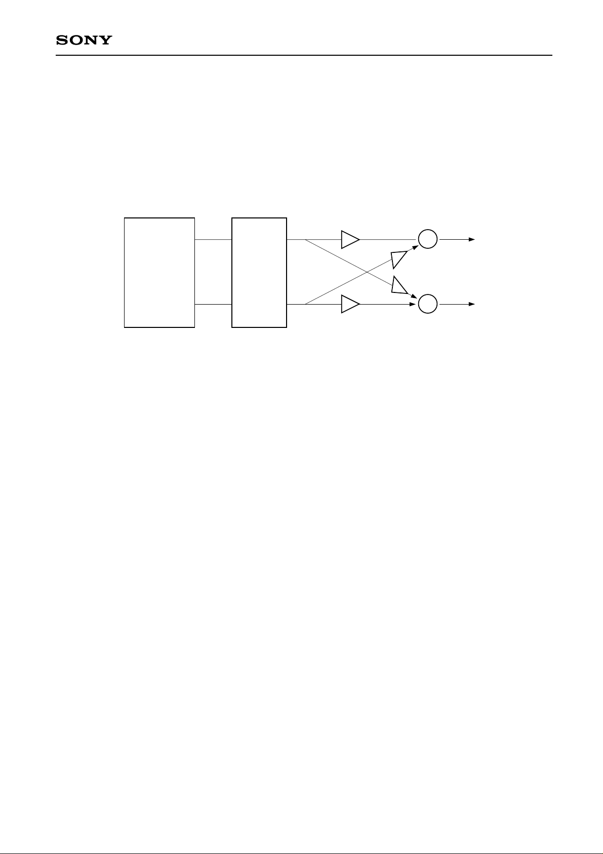
2.1.27. ATV (attenuation value) register 0
2.1.28. ATV (attenuation value) register 1
2.1.29. ATV (attenuation value) register 2
2.1.30. ATV (attenuation value) register 3
The attenuation values are set in these registers.
ATV0
CXD1803AQ/AR
+
L
ADPCM
DECODER
DF
ATV2
ATV3
ATV1
+
R
Setting 81HEX or higher in these registers is prohibited. When bits 7 to 0 of these registers are "b7" to
"b0", the attenuation (dB) is as follows:
Attenuation = 201og (b7×20+b6×2-1+b5×2-2+b4×2-3+b3×2-4+b2×2-5+b1×2-6+b0×2
7
The relationship expressed in the above formula and ATV register settings are given in the following
table.
—33—
Page 34
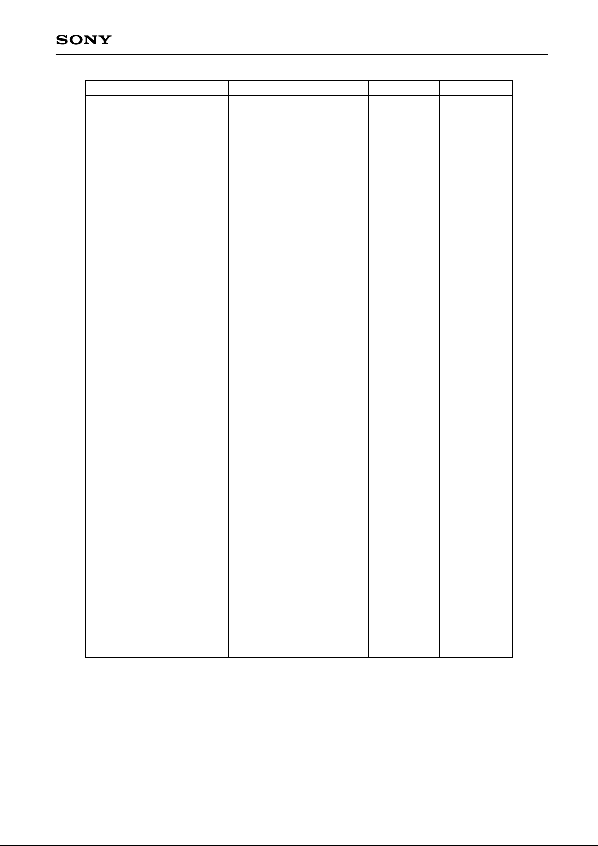
CXD1803AQ/AR
Setting Attenuation Setting Attenuation Setting Attenuation
80 0.00 55 3.56 2A 9.68
7F 0.07 54 3.66 29 9.89
7E 0.14 53 3.76 28 10.10
7D 0.21 52 3.87 27 10.32
7C 0.28 51 3.97 26 10.55
7B 0.35 50 4.08 25 10.78
7A 0.42 4F 4.19 24 11.02
79 0.49 4E 4.30 23 11.26
78 0.56 4D 4.41 22 11.51
77 0.63 4C 4.53 21 11.77
76 0.71 4B 4.64 20 12.04
75 0.78 4A 4.76 1F 12.32
74 0.86 49 4.88 1E 12.60
73 0.93 48 5.00 1D 12.90
72 1.01 47 5.12 1C 13.20
71 1.08 46 5.24 1B 13.52
70 1.16 45 5.37 1A 13.84
6F 1.24 44 5.49 19 14.19
6E 1.32 43 5.62 18 14.54
6D 1.40 42 5.75 17 14.91
6C 1.48 41 5.89 16 15.30
6B 1.56 40 6.02 15 15.70
6A 1.64 3F 6.16 14 16.12
69 1.72 3E 6.30 13 16.57
68 1.80 3D 6.44 12 17.04
67 1.89 3C 6.58 11 17.54
66 1.97 3B 6.73 10 18.06
65 2.06 3A 6.88 0F 18.62
64 2.14 39 7.03 0E 19.22
63 2.23 38 7.18 0D 19.87
62 2.32 37 7.34 0C 20.56
61 2.41 36 7.50 0B 21.32
60 2.50 35 7.66 0A 22.14
5F 2.59 34 7.82 09 23.06
5E 2.68 33 7.99 08 24.08
5D 2.77 32 8.16 07 25.24
5C 2.87 31 8.34 06 26.58
5B 2.96 30 8.52 05 28.16
5A 3.06 2F 8.70 04 30.10
59 3.16 2E 8.89 03 32.60
58 3.25 2D 9.08 02 36.12
57 3.35 2C 9.28 01 42.14
56 3.45 2B 9.47 00 ∞
Relationship between ATV register settings and attenuation amounts
All written registers, except the ATV0 and ATV2 registers, are 00HEX when the IC is reset (both hard and soft
reset). The ATV0 and ATV2 registers are 80HEX when the IC is reset. "Hard reset" means that the XRST pin
is set low. "Soft reset" means that the sub CPU resets the IC.
—34—
Page 35

2.2. Read registers
In the descriptions of the ECCSTS, DECSTS, HDRFLG, HCR, SHDR and CMADR-H registers, the
current sector denotes the sector for which these registers are valid for the decoder interrupt
(DECINT). In the monitor-only or write-only mode, the sector sent from the CD DSP immediately
before the decoder interrupt is called the current sector. In the real-time correction mode and repeat
correction mode, the current sector is that in which error detection correction has been completed.
2.2.1. ECCSTS (ECC status)
bit 7: EDCALL0 (EDC ALL 0)
This is high when there are no error flags in all the 4 EDC parity bytes of the current sector
and their values are all 00h.
bit 6: ERINBLK (erasure in block)
(1) When the decoder is operating in the monitor-only, write-only or real-time mode which
prohibits erasure correction, this indicates that at least a 1-byte error flag (C2PO) has
been raised in the data excluding the sync mark from the current sector CD DSP.
(2) When the decoder is operating in the real-time correction mode which performs
erasure correction, this indicates that at least a 1-byte error flat (MDBP) has been
raised in the data excluding the sync mark from the current sector CD DSP.
bit 5: CORINH (correction inhibit)
This is high if the current sector MODE and FORM could not be determined when the
AUTODIST bit of the DECCTL register is set high. ECC or EDC is not executed in this
sector. The CORINH bit is invalid when AUTODIST is set low. It is high in any of the
conditions below when the AUTODIST bit is set high.
(1) When the C2 pointer of the MODE byte is high
(2) When the MODE byte is a value other than 01HEX or 02HEX.
(3) When the MODE byte is 02HEX and the C2 pointer is high in the submode byte
bit 4: CORDONE (correction done)
Indicates that there is an error corrected byte in the current sector.
bit 3: EDCOK
Indicates that an EDC check has found no errors in the current sector.
bit 2: ECCOK
Indicates that there are no more errors from the header byte to P parity byte in the current
sector. (Bit 2 = don't care in the MODE2, FORM2 sectors.)
CXD1803AQ/AR
EDCOK ECCOK Description
L L Error(s) present in current sector
(1), (2) or (3) applies:
LH
(1) ECD overlooked
(2) Error corrected
(3) Error(s) present in header byte with FORM2
(1) EDC overlooked,
HLor
(2) Error(s) present in P parity byte
H H No error(s) in current sector
—35—
Page 36

bit 1: CMODE (correction mode)
bit 0: CFORM (correction form)
Indicates the MODE and FORM of the current sector whom the decoder has discriminated to
correct errors when the decoder is operating in the real-time correction or repeat correction
mode.
CFORM CMODE
'X' 'L' MODE1
'L' 'H' MODE2, FORM1
'H' 'H' MODE2, FROM2
2.2.2. DECSTS (decoder status) register
bit 1: SHRTSCT (short sector)
Indicates that the sync mark interval was less than 2351 bytes. This sector does not remain
in the buffer memory.
bit 0: NOSYNC
Indicates that the sync mark was inserted because one was not detected in the prescribed
position.
CXD1803AQ/AR
2.2.3. HDRFLG (header flag) register
Indicates the error flags of the header and sub header register bytes.
2.2.4. HDR (header) register
This is a 4-byte register which indicates the current sector header byte. By setting the address to
03HEX and reading out the data in sequence, the sub CPU can ascertain the values of the current
sector header bytes from the MINUTE byte.
2.2.5. SHDR (sub header) register
This is a 4-byte register which indicates the current sector sub header byte. By setting the address to
04HEX and reading out the data in sequence, the sub CPU can ascertain the values of the current
sector sub header bytes from the File byte.
The contents of the HDRFLG, HDR and SHDR registers indicate:
(1) The corrected value in the real-time correction or repeat correction mode
(2) Value of the raw data from the drive in the monitor-only or write-only mode
The CMOME and CMODE bits (bits 1, 0) of ECCSTS indicate the FORM and MODE of the sector the
decoder has discriminated by the raw data from the drive. Due to erroneous corrections, the values of
these bits may be at variance with those of the HDR register MODE byte and SHDR register submode
byte bit 5.
—36—
Page 37

2.2.6. CMADR-H (current minute address high) register
Indicates the upper 8 bits of the buffer memory in which the current sector (after completion of
correction) minute byte is written. (The lower 10 bits are 00HEX.)
2.2.7. INTSTS (interrupt status) register
The value of each bit in this register indicates that of the corresponding interrupt status. These bits
are not affected by the values of the INTMSK register bits.
bit 7: DRVOVRN (drive overrun)
bit 6: DECTOUT (decoder time out)
bit 4: RTADPEND (real-time ADPCM end)
bit 3: HDMACMP (host DMA complete)
bit 2: DECINT (decoder interrupt)
bit 1: BFWRDY (buffer write ready)
bit 0: BFEMPT (buffer empty)
2.2.8. RDDATA (CPU buffer read data)
The buffer data is read out from this register.
CXD1803AQ/AR
2.2.9. ADPCI (ADPCM coding information) register
bit 7: MUTE
This is high when the DA data is muted.
bit 6: EMPHASIS
This is high when emphasis is applied to the ADPCM data.
bit 5: ADPBUSY
This is high for ADPCM decoding.
bit 4: BITLNGTH (bit length)
Indicates the bit length of the coding information for ADPCM playback.
High: 8 bits
Low: 4 bits
bit 3: SMADPBSY (sound map ADPCM busy)
This is high during sound map ADPCM playback.
bit 2: FS (sampling frequency)
Indicates the sampling frequency of ADPCM playback.
High: 18.9 kHz
Low: 37.8 kHz
bit 1: RTADPBSY (real-time ADPCM busy)
This is high during real-time ADPCM playback.
bit 0: S/M (stereo/monaural)
Indicates the coding information stereo or monaural for ADPCM playback.
High: stereo
Low: monaural
2.2.10. HXFRC-L (host transfer counter-low)
—37—
Page 38

2.2.11. HXFRC-H (host transfer counter-high)
The HXFRC counter indicates the number of remaining bytes in the data to be transferred between the
SCSI controller and the buffer memory. If sound map data is to be transferred before the data is
transferred (immediately after the sub CPU has set the BFRD and BFWR bits (bits 7 and 6) of the
DMACTL register high), 2304 (900HEX) is loaded into HXFRC. At any other time, the HXFR value is
loaded. HXFRC is decremented when data is read from the buffer memory (BFRD is high) or when
the IC accepts data from the SCSI controller (BFWR is high).
Therefore, the sub CPU cannot read the HXFRC value during transfer of data between the SCSI
controller and the IC. The values of HXDRC and the write register HXFR are almost always different.
2.2.12. HADRC-L (host address counter-low)
2.2.13. HADRC-M (host address counter-middle)
This counter keeps the addresses which write or read the data with the SCSI controller into/from the
buffer. If sound map data is to be transferred before the data is transferred, any of 600CHEX, 6A0CHEX
or 740CHEX (when connected to 32K-byte buffer memory) is loaded into HADRC. At any other time,
the HADR (sub CPU register) value is loaded.
When data from the SCSI controller is written into the buffer or data to the SCSI controller is read from
the buffer, the HADRC value is output from MA0 to 16. HADRC is incremented each time one byte of
data from the drive is read from the buffer (BFRD is high) or written into the buffer (BFWR is high).
Therefore, the sub CPU cannot read the HADRC value during transfer of data between the SCSI
controller and the IC. The values of HADRC and the write register HADR are almost always different.
The upper two bits of HADRC are in HXFRC-H.
CXD1803AQ/AR
2.2.14. DADRC-L
2.2.15. DADRC-M
The DADRC value is incremented before the data from the drive is written into buffer memory.
Therefore, the sub CPU can not read the DADRC value during decoder write-only or repeat correction
modes.
The upper two DADRC bits are in HXFRC-H.
2.2.16. CADRC-L
2.2.17. CADRC-M
2.2.18. CADRC-H
bit 6: CBFRDRDY (sub CPU buffer read ready)
bit 5: CBFWRRDY (sub CPU buffer write ready)
bit 2: CADRC17
bit 1: PDATA (pointer data)
bit 0: CADRC16
The sub CPU can read the RDDATA register when this bit is high.
The sub CPU can write in the WRDATA register when this bit is high.
CADRC bit 17 (MSB).
The buffer memory pointer bit value can be read from this bit.
CADRC bit 16.
—38—
Page 39
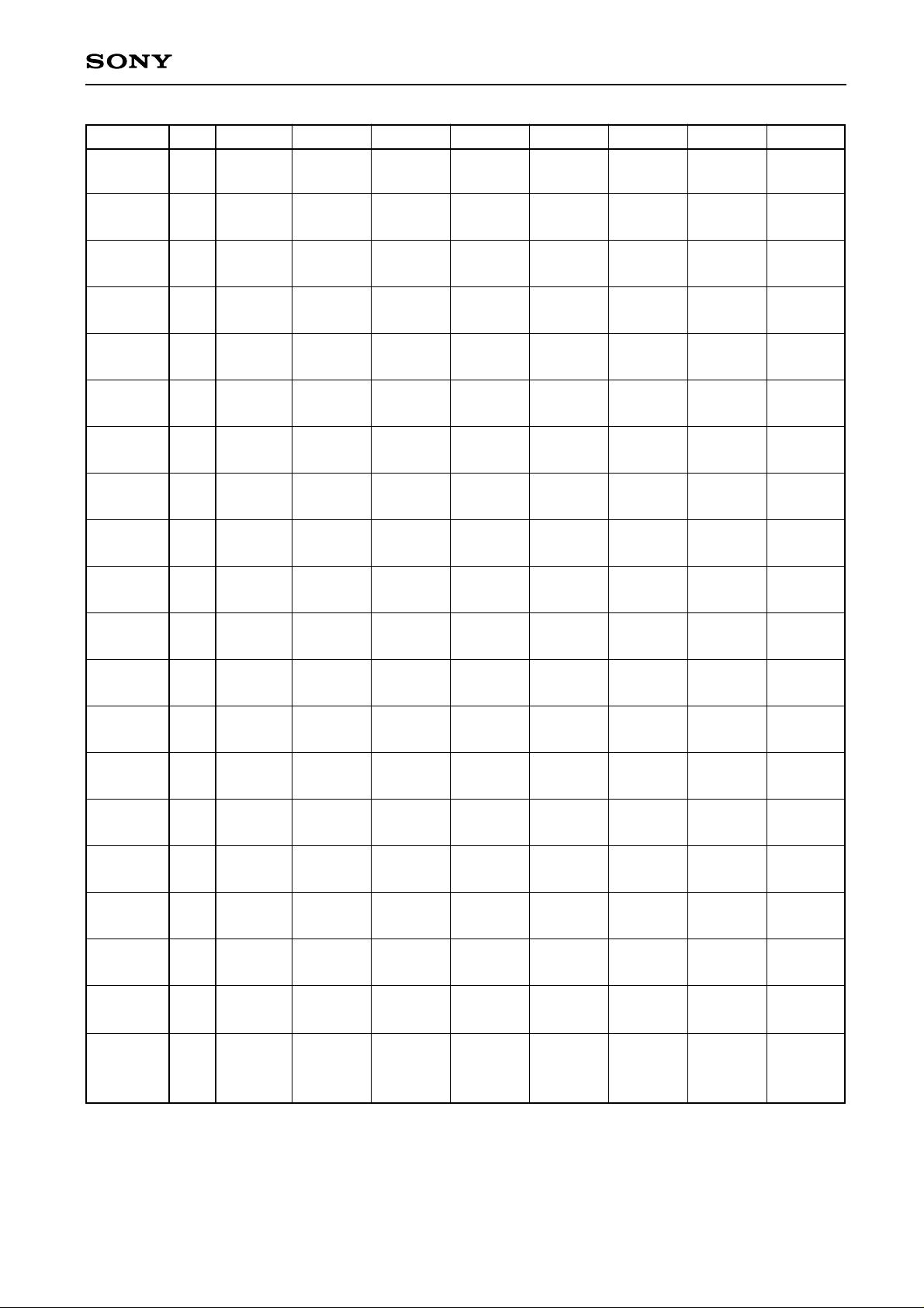
CXD1803AQ/AR
REG ADR bit7 bit6 bit5 bit4 bit3 bit2 bit1 bit0
DRVIF 00
CONFIG
1 SZ1 SZ0 RAM DIS DIS
CONFIG
2 1 0 CTL CTL BF2 DIS EN CTL
01 'L' XSLOW 'L'
02
DECCTL 03
DLADR
-L
DLADR
-M
DLADR
-H
04 bit7 bit6 bit5 bit4 bit3 bit2 bit1 bit0
05 bit15 bit14 bit13 bit12 bit11 bit10 bit9 bit8
06 'L' 'L' 'L' 'L' 'L' 'L' bit17 bit16
CHPCTL 07
C2PO LCH BCK BCK BCK LSB
L1st LOW RED MD1 MD0 1st
'L' 'L'
RAM RAM 9bit CLK HCLK
SCYC SCYC SPE SPMJ SM DAMIX DACOUT PRTY
EN ECC MODE FROM AUTO DEC DEC DEC
DLADR STR SEL SEL DIST MD2 MD1 MD0
SM RT CDDA CD- SW RPS DBL
MUTE MUTE MUTE DA OPEN TART SPD
'L'
WRDATA 08 bit7 bit6 bit5 bit4 bit3 bit2 bit1 bit0
INTMSK 09
CLRCTL 0A
CLRINT 0B
HXFR
-L
HXFR
-H HXFRC bit17 bit16
HADR
-L
HADR
-M
DADRC
-L
DADRC
-M
DADRC
-H
0C bit7 bit6 bit5 bit4 bit3 bit2 bit1 bit0
0D
0E bit7 bit6 bit5 bit4 bit3 bit2 bit1 bit0
0F bit15 bit14 bit13 bit12 bit11 bit10 bit9 bit8
10 bit7 bit6 bit5 bit4 bit3 bit2 bit1 bit0
11 bit15 bit14 bit13 bit12 bit11 bit10 bit9 bit8
12 'L' 'L' 'L' 'L' 'L' 'L' bit17 bit16
DRV DEC
OVRN TOUT END CMP INT WRDY EMPT
CHP
RST CLR CLR DATA SYNC
'L' 'L'
DRV DEC
OVRN TOUT END CMP INT WRDY EMPT
DIS
'L'
'L'
'L'
HADR HADR
RTADP HDMA DEC BF BF
RTADP SMADP
'L'
PRE
RTADP HDMA DEC BF BF
bit11 bit10 bit9 bit8
13
| 'L' 'L' 'L' 'L' 'L' 'L' 'L' 'L'
14
Sub CPU write registers (1)
—39—
Page 40

CXD1803AQ/AR
REG ADR bit7 bit6 bit5 bit4 bit3 bit2 bit1 bit0
CADRC
-L
CADRC
-M
CADRC
-H SRC EN
15 bit7 bit6 bit5 bit4 bit3 bit2 bit1 bit0
16 bit15 bit14 bit13 bit12 bit11 bit10 bit9 bit8
17 'L'
CPU CDMA
'L' 'L' 'L' bir17 bit16
DMACTL 18 BFRD BFWR SMEN 'L' 'L' 'L' 'L' 'L'
ADPMNT 19
SMCI 1A 'L'
RTCI 1B 'L'
RTADP
EN
bit16 bit15 bit14 bit13 bit12 bit11 bit10
EMPH
ASIS LNGTH
EMPH
ASIS LNGTH bit17
'L'
'L'
BIT
BIT
'L' FS 'L' S/M
'L' FS
ADPMNT
ATV0 1C bit7 bit6 bit5 bit4 bit3 bit2 bit1 bit0
ATV1 1D bit7 bit6 bit5 bit4 bit3 bit2 bit1 bit0
ATV2 1E bit7 bit6 bit5 bit4 bit3 bit2 bit1 bit0
ATV3 1F bit7 bit6 bit5 bit4 bit3 bit2 bit1 bit0
Sub CPU write registers (2)
S/M
—40—
Page 41
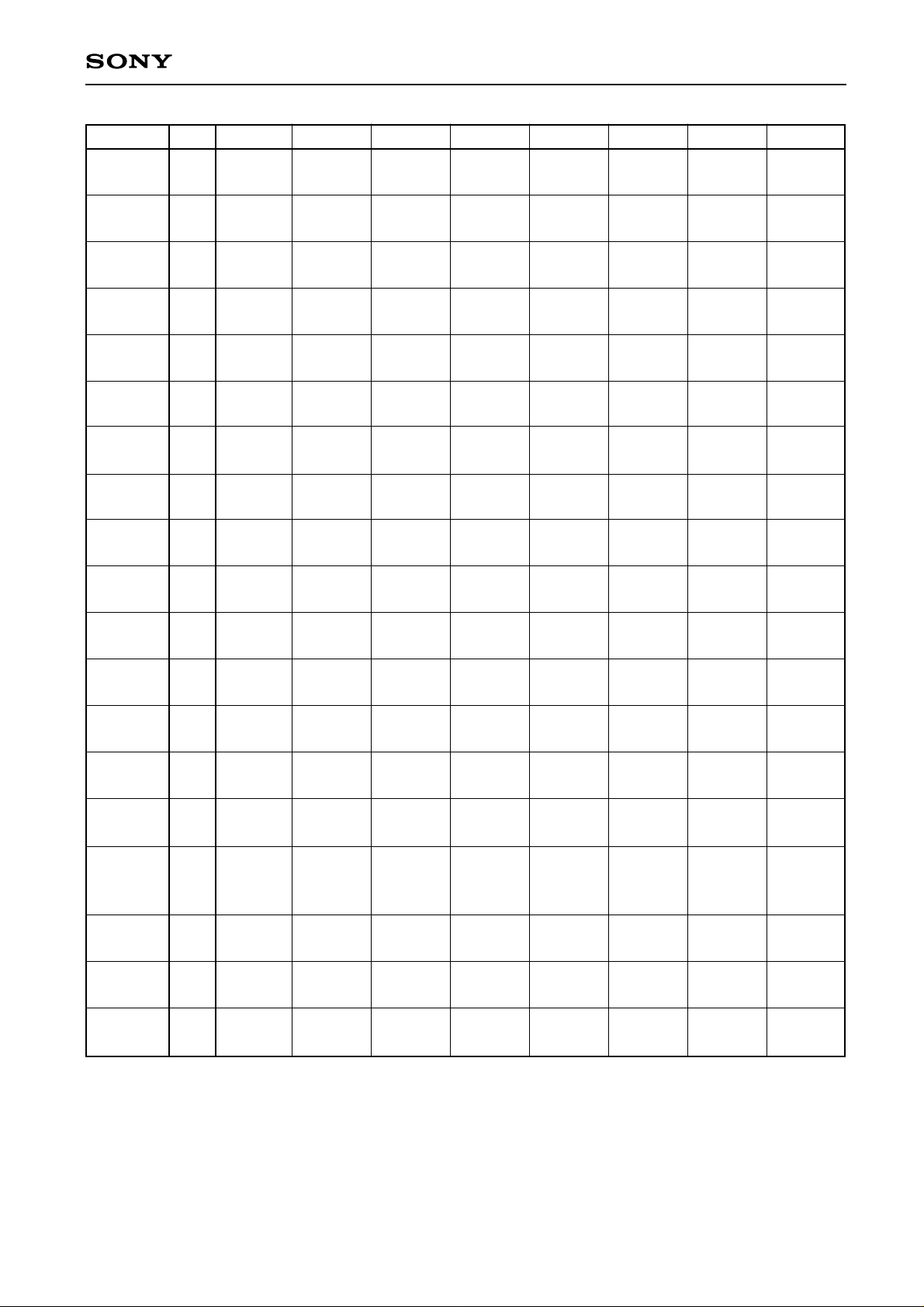
CXD1803AQ/AR
REG ADR bit7 bit6 bit5 bit4 bit3 bit2 bit1 bit0
ECCSTS 00
DECSTS 01 — — — — — —
HDRFLG 02 MIN SEC
EDC ERIN COR COR EDC ECC C C
ALL0 BLK INH DONE OK OK MODE FORM
SHRT NO
SCT SYNC
BLO
CK NEL MODE
MODE FILE
CHAN SUB
HDR 03 bit7 bit6 bit5 bit4 bit3 bit2 bit1 bit0
SHDR 04 bit7 bit6 bit5 bit4 bit3 bit2 bit1 bit0
CI
CMADR
-H
INTSTS 07
05 bit17 bit16 bit15 bit14 bit13 bit12 bit11 bit10
DRV DEC
OVRN TOUT END CMP INT WRDY EMPT
—
RTADP HDMA DEC BF BF
RDDATA 08 bit7 bit6 bit5 bit4 bit3 bit2 bit1 bit0
ADPCI 09 MUTE
HXFRC
-L
HXFRC
-H bit17 bit17 bit16 bit16
HADRC
-L
HADRC
-M
DADRC
-L
DADRC
-M
0A bit7 bit6 bit5 bit4 bit3 bit2 bit1 bit0
0B
DC HC DC HC
0C bit7 bit6 bit5 bit4 bit3 bit2 bit1 bit0
0D bit15 bit14 bit13 bit12 bit11 bit10 bit9 bit8
0E bit7 bit6 bit5 bit4 bit3 bit2 bit1 bit0
0F bit15 bit14 bit13 bit12 bit11 bit10 bit9 bit8
EMPH ADP BIT SMADP
ASIS BSY LNGTH BSY BSY
FS
bit11 bit10 bit9 bit8
RTADP
S/M
10
|————————
1C
CADRC
-L
CADRC
-M
CADRC
-H RDRDY WRDRY DATA
1D bit7 bit6 bit5 bit4 bit3 bit2 bit1 bit0
1E bit15 bit14 bit13 bit12 bit11 bit10 bit9 bit8
1F
CBF CBF
— — bit17
P
bit16
Sub CPU read registers
For HXFRC-H, DC and HC represent DADRC and HASRC respectively.
—41—
Page 42
CXD1803AQ/AR
3. Connection with Buffer Memory
3.1.Memory types
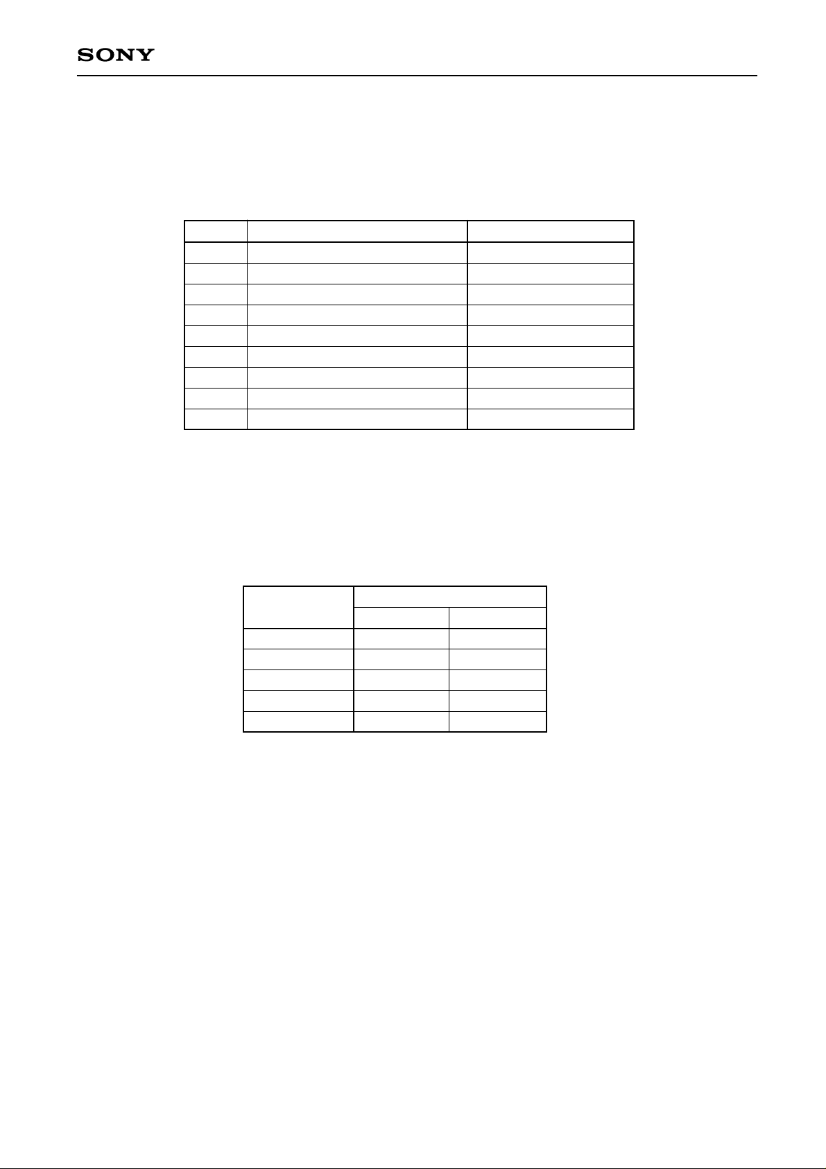
The DRAM pin input, CNFIG1 register RAMSZ1, RAMSZ0 and 9BITRAM bits (bits 4 to 2) are set
depending on the buffer memory connected to the IC.
DRAM RAMSZ1 RAMSZ0 9BITRAM Memory size
'L' 'L' 'L' 'L' 32KW×8bSRAM
'L' 'L' 'L' 'H' 32KW×9bSRAM
'L' 'L' 'H' 'L' 32KW×8bSRAM×2
'L' 'L' 'H' 'H' 32KW×9bSRAM×2
'L' 'H' 'L' 'L' 128KW×8bSRAM
'L' 'H' 'L' 'H' 128KW×9bSRAM
'L' 'H' 'H' 'L' 128KW×8bSRAM×2
'L' 'H' 'H' 'H' 128KW×9bSRAM×2
'H' 'H' 'H' 'L' 256KW×4bDRAM×2
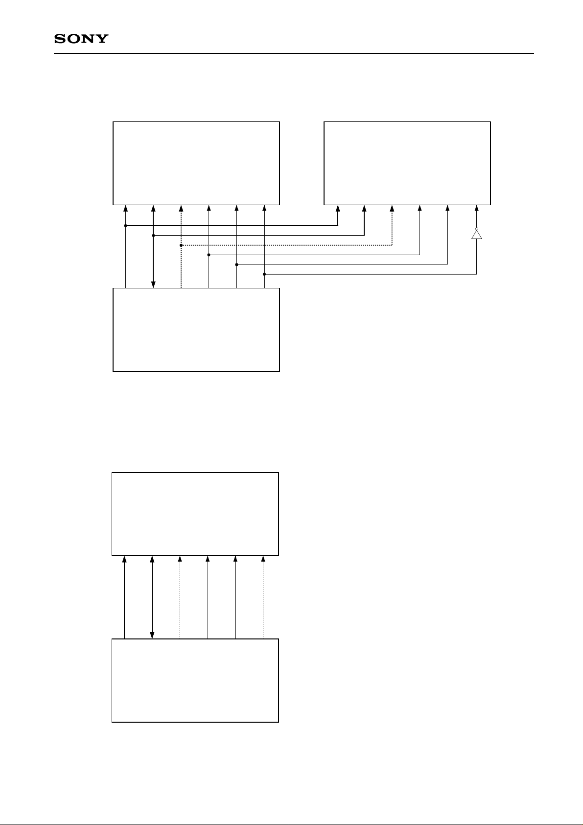
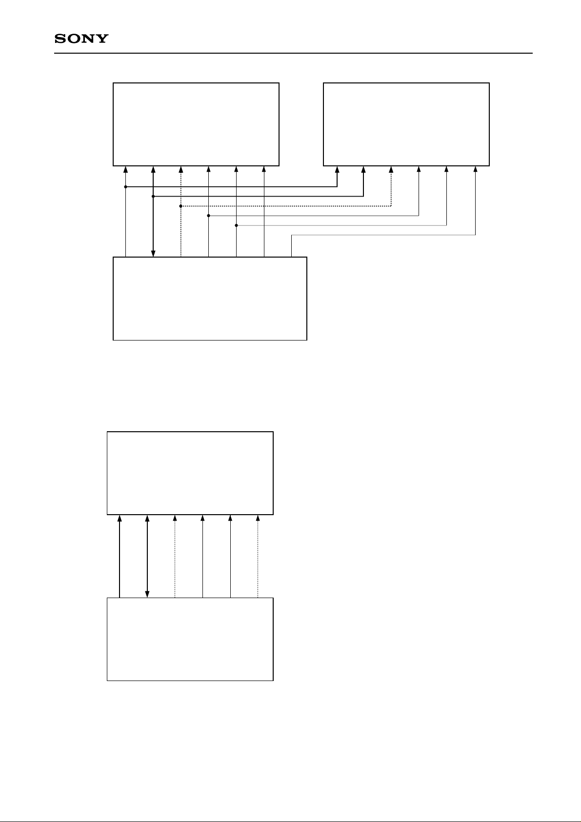
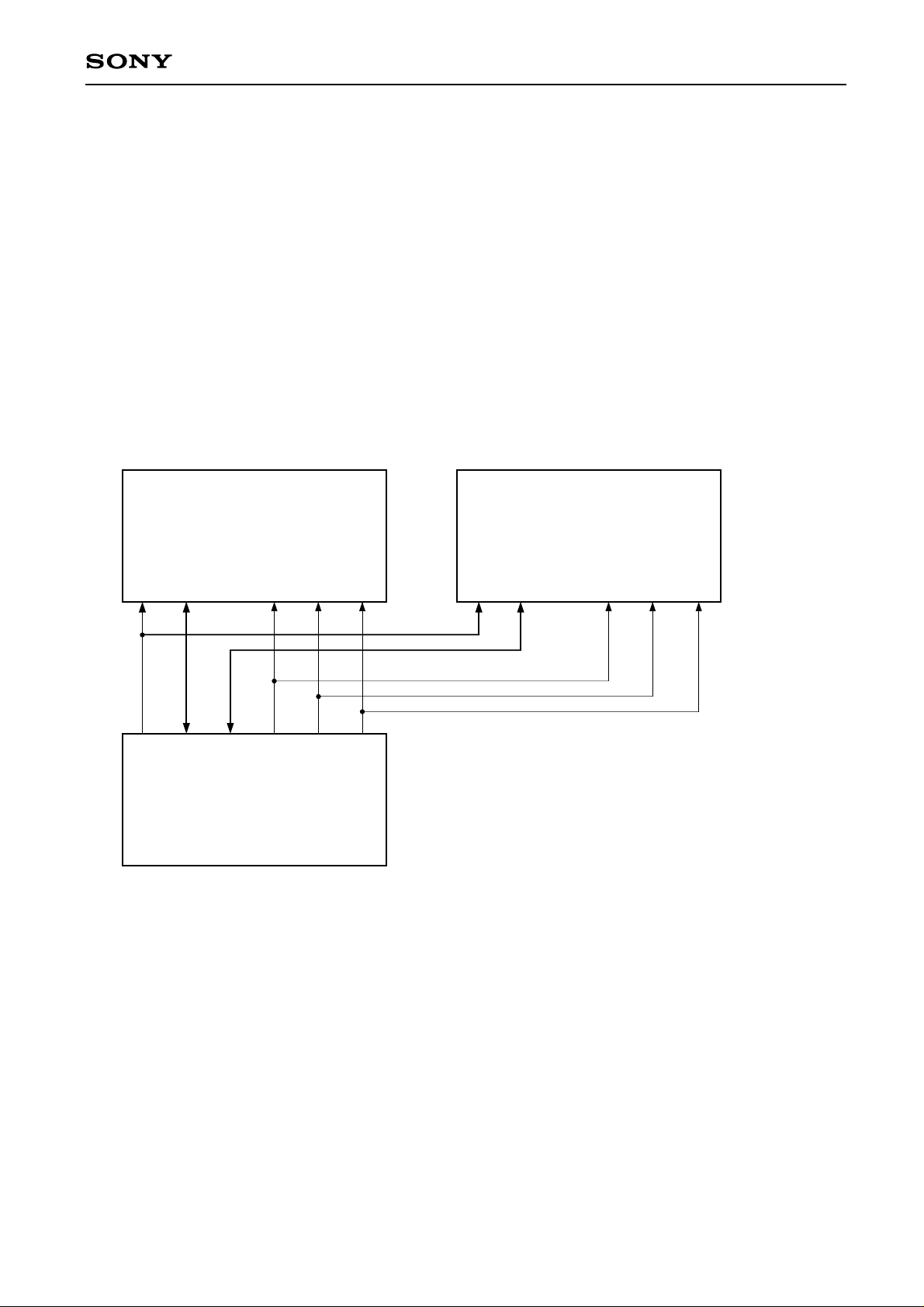
Figs. 3-1 to 3.5 show examples of connection.
3.2.Access time
The relationship between the decoder clock frequency (MHz) and minimum access time required by the
memory (preliminary value, ns) when the CONFIG1 register XSLOW is high is shown below.
Clock frequency
Access time
SRAM DRAM
16.9344 120 110
20.0000 100 90
24.0000 70 80
32.0000 50 50
33.8688 45 50
When XSLOW is low and clock frequency is 16.9344 MHz, SRAM access time is 500 ns and DRAM
access time is 300 ns.
—42—
Page 43
CXD1803AQ/AR
A14 to 0
MA14 to 0
CXD1803AQ/AR 32KB SRAM
I/O9
I/O8 to 1
MDBP
MDB7 to 0
/WR
/OE
∗1
XMOE
XMWR
/CE
MA15
32KB SRAM
A14 to 0
I/O8 to 1
I/O9
/OE
/WR
/CE
Fig. 3-2 Connection to 64K-byte SRAM
A14 to 0
MA14 to 0
CXD1803AQ/AR 32KB SRAM
I/O8 to 1
I/O9
MDBP
MDB7 to 0
/WR
/OE
∗1
XMOE
XMWR
/CE
∗2
XME0
Fig. 3-1 Connection to 32K-byte SRAM
1 Connect to 9 bits / word SRAM when performing erasure correction.
2 Connect /CE to XME0 or ground.
∗
∗
—43—
Page 44
CXD1803AQ/AR
A14 to 0
MA14 to 0
CXD1803AQ/AR 128KB SRAM
I/O8 to 1
I/O9
MDBP
MDB7 to 0
/WR
/OE
∗1
XMOE
XMWR
/CE1
XME0
128KB SRAM
XME1
A14 to 0
I/O8 to 1
I/O9
/OE
/WR
/CE1
Fig. 3-4 Connection to 256K-byte SRAM
A16 to 0
MA16 to 0
CXD1803AQ/AR 128KB SRAM
I/O8 to 1
I/O9
MDBP
MDB7 to 0
/WR
/OE
∗1
XMOE
XMWR
/CE1
∗2
XME0
Fig. 3-3 Connection to 128K-byte SRAM
1 Connect to x9 SRAM when performing erasure correction.
2 Connect /CE1 to XME0 or ground.
∗
3 Connect CE2 to VDD.
∗
∗
—44—
Page 45
CXD1803AQ/AR
128KB DRAM
A8 to 0
MA8 to 0
CXD1803AQ/AR
I/O4 to 1
MDB7 to 4
MDB3 to 0
/RAS
XRAS
/CAS
XCAS
/WE
XMWR
128KB DRAM
A8 to 0
I/O4 to 1
/RAS
/CAS
/WE
Fig. 3-5 Connection to 256K-byte DRAM
4 Connect DRAM /OE pin to ground.
∗
—45—
Page 46
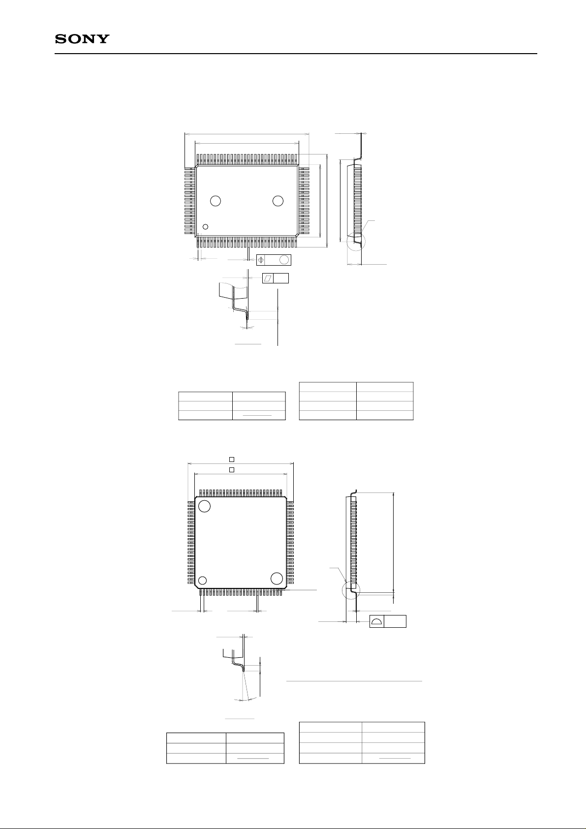
Package Outline Unit : mm
CXD1803AQ/AR
CXD1803AQ
SONY CODE
EIAJ CODE
JEDEC CODE
0.65
0° to 15°
100PIN QFP (PLASTIC)
23.9 ± 0.4
+ 0.4
20.0 – 0.1
±0.12
M
0.15
(16.3)
DETAIL A
QFP-100P-L01
∗QFP100-P-1420-A
0.8 ± 0.2
+ 0.1
0.15 – 0.05
+ 0.4
15.8 ± 0.4
17.9 ± 0.4
14.0 – 0.01
PACKAGE STRUCTURE
PACKAGE MATERIAL
LEAD TREATMENT
LEAD MATERIAL
PACKAGE WEIGHT
EPOXY RESIN
SOLDER PLATING
COPPER / 42 ALLOY
1.4g
A
+ 0.35
2.75 – 0.15
CXD1803AR
76
100
0.5 ± 0.08
SONY CODE
EIAJ CODE
JEDEC CODE
100PIN LQFP (PLASTIC)
16.0 ± 0.2
∗ 14.0 ± 0.1
75
1
+ 0.08
0.18 – 0.03
0.1 ± 0.1
0° to 10°
DETAIL A
LQFP-100P-L01
∗QFP100-P-1414-A
51
50
A
26
(0.22)
25
+ 0.2
1.5 – 0.1
NOTE: Dimension “∗” does not include mold protrusion.
0.5 ± 0.2
PACKAGE STRUCTURE
PACKAGE MATERIAL
LEAD TREATMENT
LEAD MATERIAL
PACKAGE WEIGHT
(15.0)
0.5 ± 0.2
+ 0.05
0.127 – 0.02
0.1
EPOXY/PHENOL RESIN
SOLDER PLATING
42 ALLOY
—46—
 Loading...