

Page 1
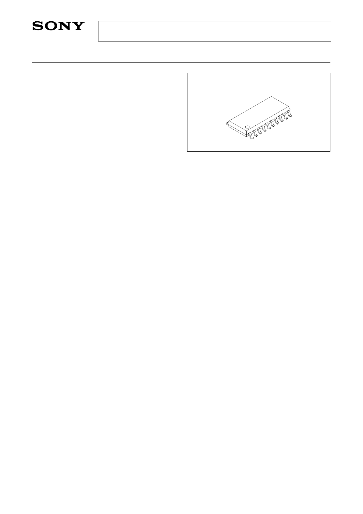
CCD Vertical Clock Driver
Description
The CXD1268M is a clock driver for CCD vertical
register drive.
Features
• On-chip 4-channel driver.
(Binary driver × 2, and trinary driver × 2)
• Low output ON resistance provides optimal drive
for large load capacity CCD.
Applications
CCD cameras
Structure
CMOS
CXD1268M
20 pin SOP (Plastic)
Absolute Maximum Ratings (GND = 0V, Ta = 25°C)
• Supply voltage VH VL to VL + 25 V
• Supply voltage VM VL to VL + 17
• Supply voltage VDD GND to GND + 7 V
• Supply voltage VL GND – 10 to GND V
• Input voltage VI –0.5 to VDD + 0.5 V
• Input/output clamp
diode current IIC, IOC –10 to +10 mA
• Maximum DC load current IODC –3 to +3 mA
• Maximum load capacity CL to 30,000 pF/pin
• Allowable power dissipation PD to 200 mW
• Storage temperature Tstg –60 to +150 °C
∗1
Use VM at less than VDD.
Recommended Operating Conditions
• Supply voltage VH VM + 6.5 to VM + 15.5 V
• Supply voltage VL VM – 10.0 to VM – 7.0 V
• Supply voltage VM 0.0 to 4.0 V
• Supply voltage VDD 4.75 to 5.25 V
∗2
∗2
3.5 to VDD V
0.0 to 1.0 V
• High level input voltage VIH
• Low level input voltage VIL
• Operating temperature Topr –10 to +60 °C
∗2
VDD = 5V
∗1
V
Sony reserves the right to change products and specifications without prior notice. This information does not convey any license by
any implication or otherwise under any patents or other right. Application circuits shown, if any, are typical examples illustrating the
operation of the devices. Sony cannot assume responsibility for any problems arising out of the use of these circuits.
– 1 –
E96635-PS
Page 2

Block Diagram
CXD1268M
V
DD
6
M1
V
3
V
16
H
XSG1
XSG2
Pin Configuration (Top View)
XV1
XV3
XV2
XV4
12
13
10
11
9
8
SG
Input
Gate
SG
Input
Gate
Level
Converter
Level
Converter
Converter
Converter
Converter
Converter
15
GND
Level
Level
Level
Level
Trinary
Driver
Trinary
Driver
Binary
Driver
Binary
Driver
20
M2
V
1
L
V
Vφ1
5
Vφ3
18
Vφ2
2
19 Vφ4
V
Vφ2
M1
V
NC
Vφ1
DD
V
NC
XV1
XSG1
XV2
L
1
2
3
4
5
6
7
8
9
10
20
19
18
17
16
15
14
13
12
11
M2
V
Vφ4
Vφ3
NC
H
V
GND
NC
XV3
XSG2
XV4
– 2 –
Page 3

Pin Description
CXD1268M
Pin No.
1
2
3
4
5
6
7
8
9
10
11
12
13
14
15
16
Symbol I/O Description
VL
Vφ2
VM1
—
Low level power supply
O
High-voltage output (2 levels: VM2, VL)
—
Middle level power supply for trinary
NC
Vφ1
VDD
O
High-voltage output (3 levels: VH, VM1, VL)
—
Input section power supply
NC
XV1
XSG1
XV2
XV4
XSG2
XV3
I
Output control (Vφ1)
I
Output control (Vφ1)
I
Output control (Vφ2)
I
Output control (Vφ4)
I
Output control (Vφ3)
I
Output control (Vφ3)
NC
GND
VH
—
GND
—
High level power supply for trinary
17
18
19
20
Truth Table
XV1, XV3
H
H
L
L
X
X
NC
Vφ3
Vφ4
VM2
O
O
—
Input
XSG1, XSG2 XV2, XV4
L
H
L
H
X
X
High-voltage output (3 levels: VH, VM1, VL)
High-voltage output (2 levels: VM2, VL)
Middle level power supply for binary
X: Don’t care
Output
Vφ1, Vφ3Vφ2, Vφ4
X
X
X
X
L
H
VL
VL
VH
VM1
X
X
X
X
X
X
VM2
VL
– 3 –
Page 4
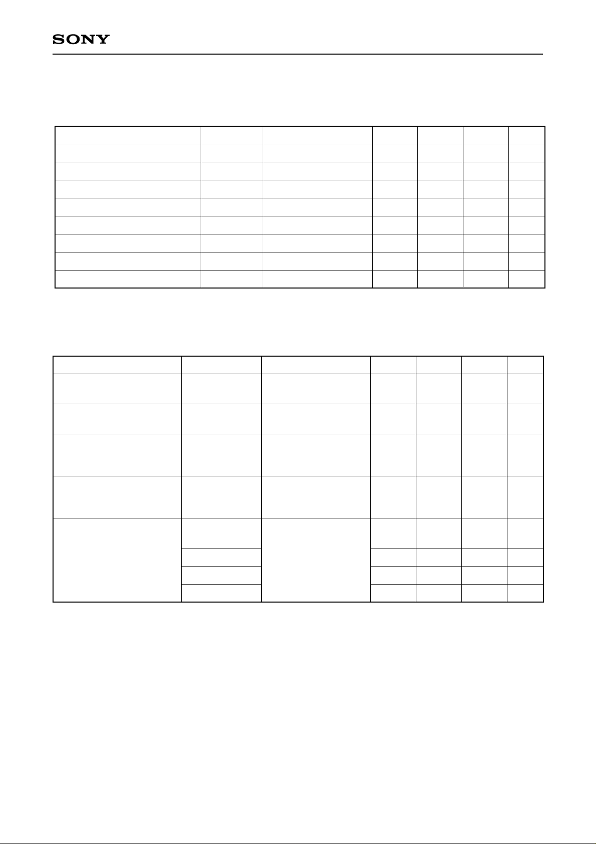
Electrical Characteristics
1. DC Characteristics
CXD1268M
(Unless otherwise specified, VH = 14.5V, VM = 1V, VDD = 5V, GND = 0V, VL = –6V,
VIL = GND, VIH = VDD, Ta = –10 to +60°C)
Item
“H” level output voltage
“M” level output voltage
“L” level output voltage
Input current
“H” level output ON resistance
“M” level output ON resistance
“L” level output ON resistance
Static current consumption
2. AC Characteristics
Item
Propagation delay time
L → M, M → L
Propagation delay time
M → H, H → M
Rise time L → M
Fall time M → L
Symbol Conditions Min. Typ. Max. Unit
VφH
VφM
VφL
II
Ron (H)
Ron (M)
Ron (L)
IDD + IH + IM
Symbol Conditions Min. Typ. Max. Unit
tPLH, tPHL
tPLH, tPHL
tTLH, tTHL
IφH = –1mA
IφM = –1mA
IφL = 1mA
IφH = –50mA
IφM = –50mA
IφL = 50mA
Waveform diagram (1),
no load
Waveform diagram (2),
no load
Refer to waveform
diagram (1), output
load circuit diagram
VH – 0.1
VM – 0.1
VL
18
18
18
10
100
200
200
–4
VH
VM
VL + 0.1
1.0
30
30
30
100
200
400
300
V
V
V
µA
Ω
Ω
Ω
µA
ns
ns
ns
Rise time M → H
Fall time H → M
Operating current
consumption
tTLH, tTHL
Idyn
(IDD + IH + IM + IL)
IDD
IH + IM
IL
Refer to waveform
diagram (2), output
load circuit diagram
Refer to input pulse
timing diagram, output
load circuit diagram
–5.0
200
6.0
0.02
3.8
–3.8
300
10.0
0.2
5.0
ns
mA
mA
mA
mA
– 4 –
Page 5
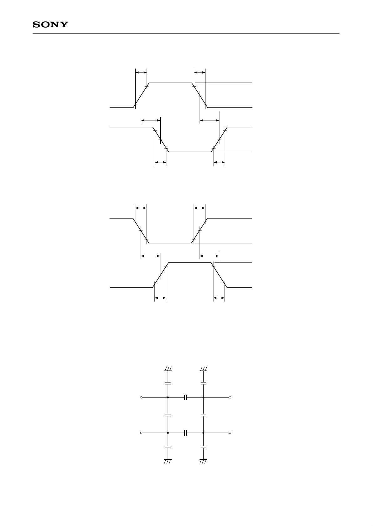
Waveform Diagram (1)
CXD1268M
tr tf
input
XV1 to XV4
output
Vφ1 to Vφ4
Waveform Diagram (2)
input
XSG1, XSG2
output
Vφ1, Vφ3
90%
50%
10%
90%
tr tf
90%
50%
10%
PLH tPHL
t
50%
10%
tTLH tTHL
50%
10%
90%
VDD
tr = tf = 20ns
GND
PLHtPHL
t
VφM
tTLHtTHL
VφL
VDD
tr = tf = 20ns
GND
VφH
VφM
Output Load Circuit Diagram
1600pF 2000pF
1000pF
Vφ1
3000pF 3000pF
1000pF
2000pF 1600pF
– 5 –
Vφ4
Vφ3Vφ2
Page 6
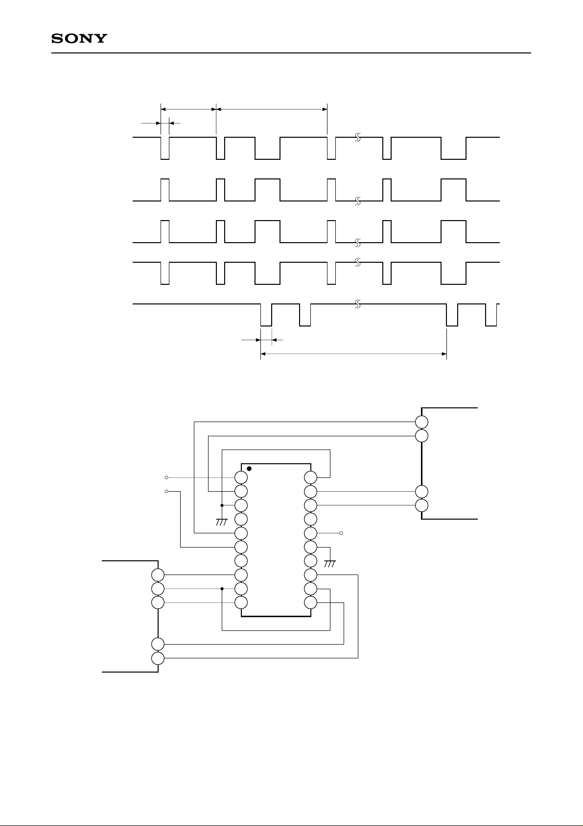
Input Pulse Timing Diagram
2µs
XV1
XV2
XV3
XV4
XSG1, XSG2
CXD1268M
63.5µs 127µs
Application Circuit
timing generator
XV1
XSG
XV2
–7.5V
5V
10
9
1
2
3
4
5
6
7
8
5µs
V
L
Vφ2
M1
V
NC
Vφ1
DD
V
NC
XV1
XSG1
XV2
M2
V
Vφ4
Vφ3
NC
V
GND
NC
XV3
XSG2
XV4
15.7ms
CCD image sensor
Vφ1
Vφ2
20
19
18
17
H
16
15
14
13
12
11
15V
Vφ4
Vφ3
XV4
XV3
Application circuits shown are typical examples illustrating the operation of the devices. Sony cannot assume responsibility for
any problems arising out of the use of these circuits or for any infringement of third party patent and other right due to same.
Notes on Operation
1. When applying power, be sure to apply VH before VDD and VM.
2. XSG1 (Pin 9) and XSG2 (Pin 12) can be input separately, although they are also common input.
– 6 –
Page 7
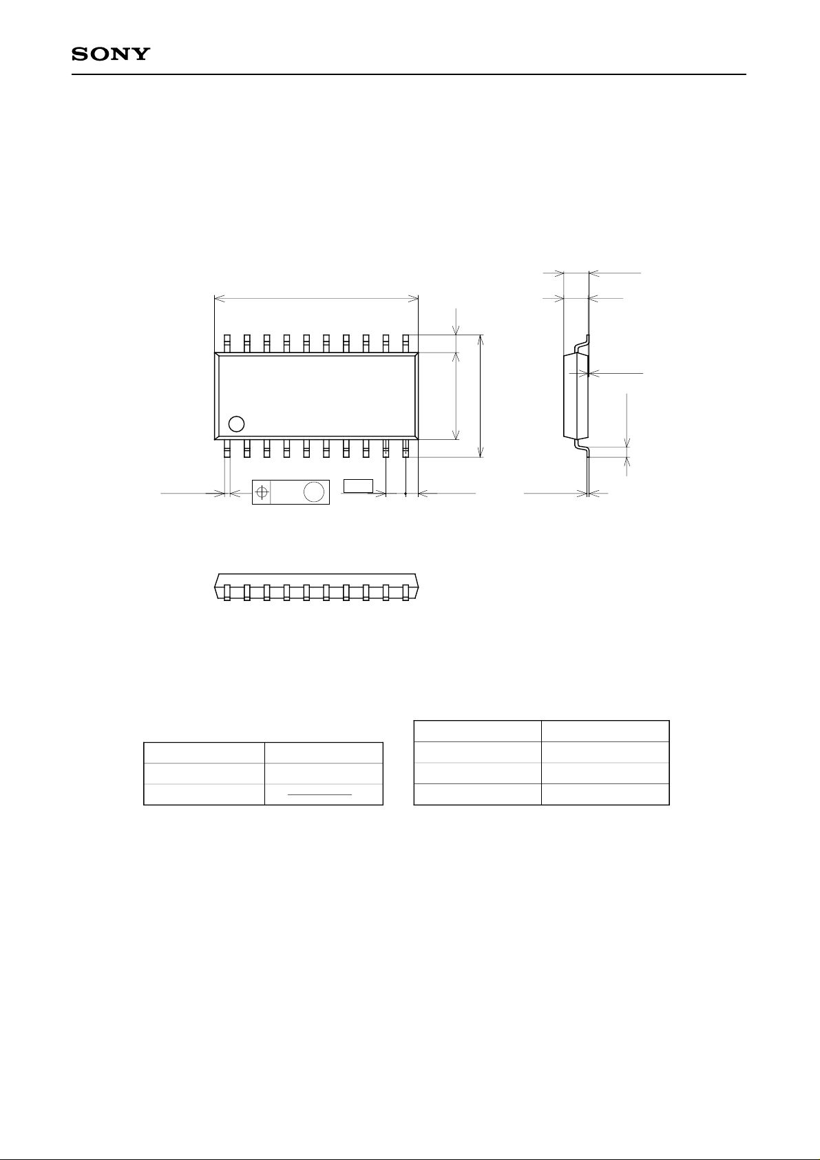
Package Outline Unit: mm
CXD1268M
20PIN SOP (PLASTIC)
1.8MAX
+ 0.1
0.4 – 0.05
20
1
13.0MAX
0.12
1.55
11
1.1
5.6
7.7 ± 0.3
0.1 ± 0.1
0.6 ± 0.2
10
1.27
M
0.78MAX
+ 0.1
0.2 – 0.05
SONY CODE
EIAJ CODE
JEDEC CODE
SOP-20P-L071
SOP020-P-0300
PACKAGE STRUCTURE
PACKAGE MATERIAL
LEAD TREATMENT
LEAD MATERIAL
PACKAGE MASS
– 7 –
EPOXY RESIN
SOLDER PLATING
COPPER ALLOY
0.3g
 Loading...