

Page 1

CCD Camera Timing Generator
Description
The CXD1265R generates the timing pulses
required by the CCD image sensors as well as
signal processing circuits.
Features
• NTSC and PAL compatible
• Compatible with digital and analog camera
systems
• Black-and-white mode compatible
(EIA/CCIR compatible)
• Electronic shutter function
• H-driver
• Standby function
• Compatible with field/frame accumulation
modes
∗1
∗2
∗1, ∗2
Characteristics of CCD image sensor are
guaranteed by field accumulation.
Low speed shutter can not be used during frame
accumulation mode.
CXD1265R
64 pin LQFP (Plastic)
Absolute Maximum Ratings (Ta = 25°C)
• Supply voltage VDD Vss – 0.5 to +7.0 V
• Input voltage VI Vss – 0.5 to VDD + 0.5 V
• Output voltage VO Vss – 0.5 to VDD + 0.5 V
• Operating temperature Topr –20 to +75 °C
• Storage temperature Tstg –55 to +150 °C
• Supply voltage VEE –5 to Vss V
• Allowable power dissipation
PD 500 mW
Applications
CCD cameras
Structure
Silicon gate CMOS IC
Applicable CCD Image Sensors
ICX038BNA, ICX038BNB, ICX038BLA
ICX039BNA, ICX039BNB, ICX039BLA
ICX058AK, ICX058AKB, ICX058AL
ICX059AK, ICX059AKB, ICX059AL
Block Diagram
62
VD INITIALIZE
60
SYNC
GEN
59
57
63
64
1
2
41
42
43
44
45
46
22
37
HD INITIALIZE
HIGH-SPEED
GENERATION
CIRCUIT
PULSE
38
39
1/2
23
VSS
40
28
8
ADR . COUNT
DRIVER
26
27
VDD
24
H – ROM
LATCH
GATE
10
3
56
25
DECODER
GATE
48
47
Recommended Operating Conditions
• Supply voltage VDD 5.0 ± 0.25 V
• Operating temperature Topr –20 to +75 °C
VEE
ADR . COUNT
V – ROM
LATCH
GATE
COUNTER
49
51
50
52
21
53
MODE
SET
ADR . COUNT
ROG – ROM
LATCH
SHUT
ROM
54
29
30
15
31
19
18
17
16
GATE
CONTROLLER
DECODER
32
35
33
34
20
11
12
13
14
23
36
61
HTSG
4
5
MICROCOMPUTER
6
7
9
55
58
Sony reserves the right to change products and specifications without prior notice. This information does not convey any license by
any implication or otherwise under any patents or other right. Application circuits shown, if any, are typical examples illustrating the
operation of the devices. Sony cannot assume responsibility for any problems arising out of the use of these circuits.
– 1 –
E92611C52-ST
Page 2
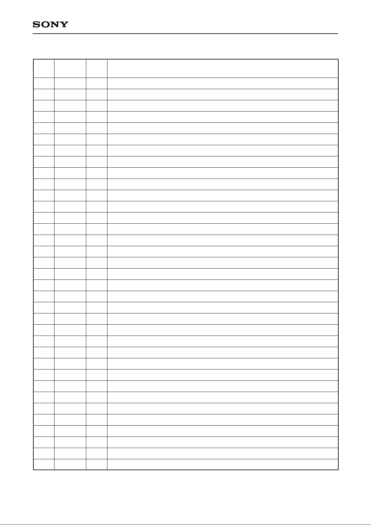
Pin Description
CXD1265R
Pin
No.
1
2
3
4
5
6
7
8
9
10
11
12
13
14
15
Symbol I/O Description
OSCO
OSCI
EF
ED0
ED1
ED2
SMD1
Vss
SMD2
XVCT
D1
D2
D3
D4
A5
O
Inverter output for oscillation.
I
Inverter input for oscillation.
I
Not used. (With pull-up resistor)
I
Shutter speed setting. Strobe input for serial mode. (With pull-up resistor)
I
Shutter speed setting. Clock input for serial mode. (With pull-up resistor)
I
Shutter speed setting. Data input for serial mode. (With pull-up resistor)
I
Shutter mode setting. (With pull-up resistor)
—
GND
I
Shutter mode setting. (With pull-up resistor)
O
Not used. (Open)
I
Fix at Low in normal operation. (With pull-down resistor)
I
Low: Color, High: Black-and-white. (With pull-down resistor)
I
Low: Field readout, High: Frame readout∗. (With pull-down resistor)
I
Low: NTSC/EIA, High: PAL/CCIR. (With pull-down resistor)
O
Not used. (Open)
16
17
18
19
20
21
22
23
24
25
26
27
28
29
30
31
32
A4
A3
A0
A1
A2
VEE
RG
NC
VDD
VDD
H1
H2
Vss
XSUB
XV2
XV1
XSG1
O
Not used. (Open)
O
Not used. (Open)
O
Not used. (Open)
O
Not used. (Open)
O
Not used. (Open)
—
GND
O
Reset gate pulse output.
—
Not used. (Open)
—
Power supply.
—
Power supply for H1 and H2.
O
Clock output for CCD horizontal register drive.
O
Clock output for CCD horizontal register drive.
—
GND for H1 and H2.
O
CCD discharge pulse output.
O
Clock output for CCD vertical register drive.
O
Clock output for CCD vertical register drive.
O
CCD sensor charge readout pulse output.
33
XV3
34
XSG2
35
XV4
∗
Characteristics of CCD image sensor are guaranteed by field accumulation.
O
Clock output for CCD vertical register drive.
O
CCD sensor charge readout pulse output.
O
Clock output for CCD vertical register drive.
– 2 –
Page 3
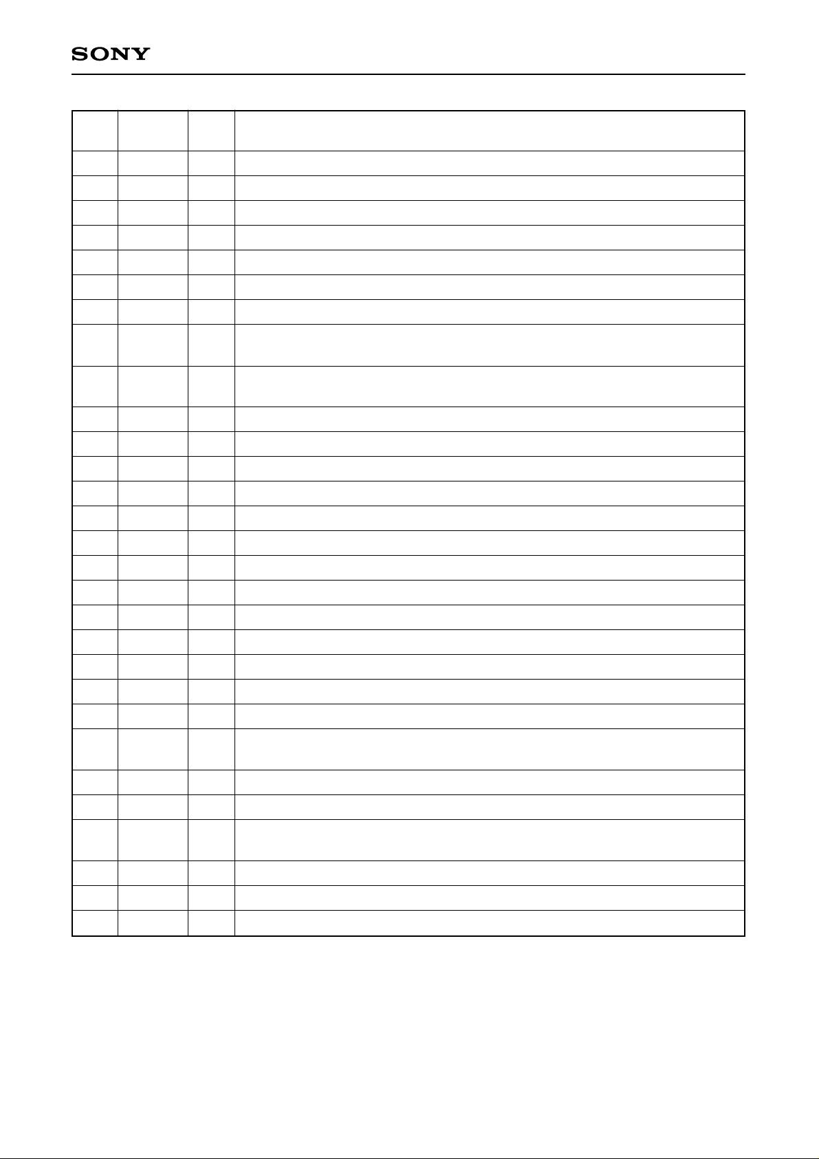
CXD1265R
Pin
No.
36
37
38
39
40
41
42
43
44
45
46
47
48
49
Symbol I/O Description
TEST2
MCK
XSHP
XSHD
Vss
XSP1
XSP2
XSH1/
SHP
XSH2/
SHD
XDL1
XDL2
BFG
CLP1
CLP2
I
Test input. Set at Low in normal operation.
O
NTSC: 910fH, PAL: 908fH. Clock output.
O
Precharge level sample-and-hold pulse.
O
Data sample-and-hold pulse.
—
GND
O
Color separation sample-and-hold pulse. Halted for black-and-white mode.
O
Color separation sample-and-hold pulse. Halted for black-and-white mode.
Switching sample-and-hold pulse/precharge level sample-and-hold pulse
O
(black-and-white mode).
Switching sample-and-hold pulse/data sample-and-hold pulse
O
(black-and-white mode).
O
Delay line clock output. Halted for black-and-white mode.
O
Delay line clock output. Halted for black-and-white mode.
O
Pulse output for chroma modulator in encoder. Halted for black-and-white mode.
O
Clamp pulse output.
I/O
Clamp pulse output. When GM is set at High, standby mode switching input.
50
51
52
53
54
55
56
57
58
59
60
61
62
63
64
CLP3
CLP4
PBLK
ID
WEN
GM
VDD
CL
PS
HD
VD
HTSG
TEST
XCK
CK
I/O
Clamp pulse output. When GM is set at High, standby mode switching input.
O
Clamp pulse output.
O
Blanking cleaning pulse output.
O
Line identification output. Halted for black-and-white mode.
O
Write enable output for low-speed shutter operation.
I
Low: Analog signal processing, High: Digital signal processing. (With pull-down resistor)
—
Power supply.
O
NTSC/EIA: 910fH, PAL/CCIR: 908fH. Clock output.
Switching for electronic shutter speed input method. (With pull-up resistor)
I
Low: Serial input, High: Parallel input.
I
Horizontal synchronizing signal input.
I
Vertical synchronizing signal input. (During Low, 9H for NTSC and 7.5H for PAL)
Control input for XSG1 and XSG2. (With pull-up resistor)
I
Low: XSG1, XSG2 halted, High: XSG1, XSG2 generated.
I
Test input. Set at Low in normal operation. (With pull-down resistor)
O
NTSC/EIA: 1820fH, PAL/CCIR: 1816fH. Clock output.
I
NTSC/EIA: 1820fH, PAL/CCIR: 1816fH. Clock input.
– 3 –
Page 4
CXD1265R
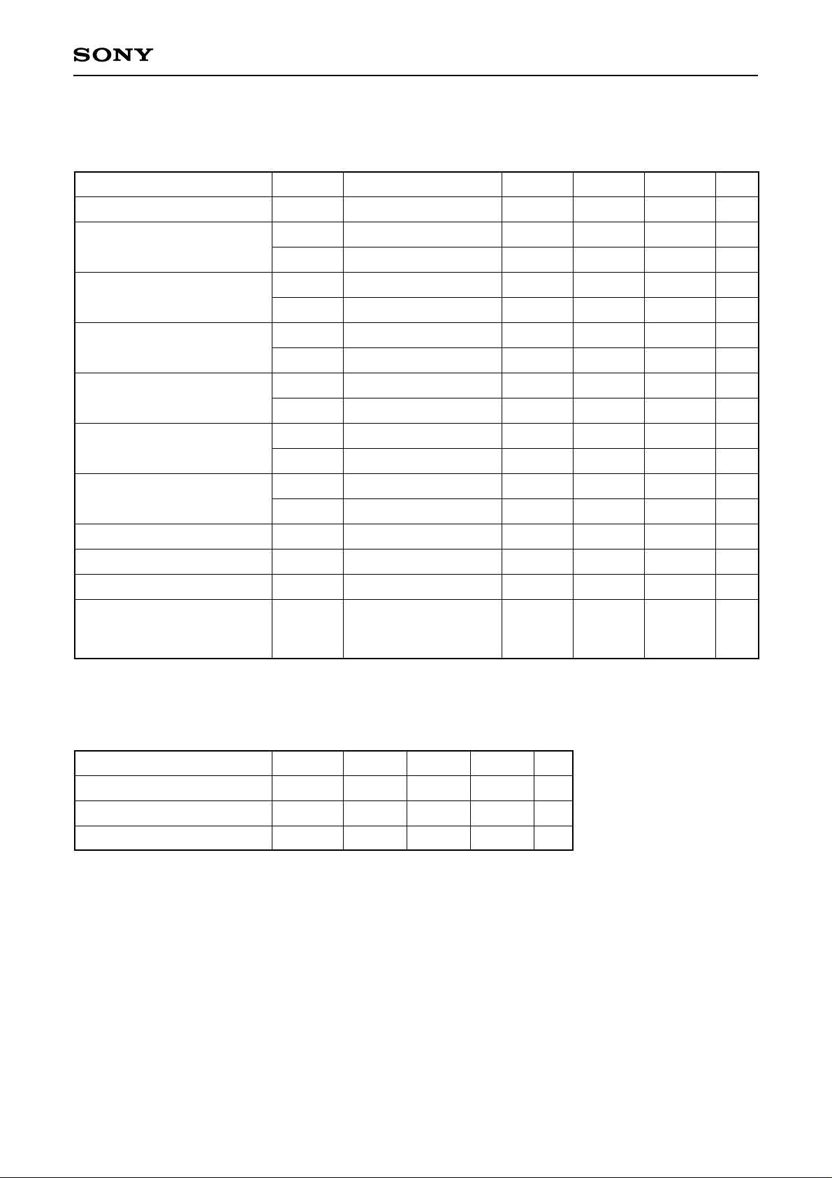
Electrical Characteristics
DC Characteristics (VDD = 5V ± 0.25V, Topr = –20 to +75°C)
Item
Symbol Conditions Min. Typ. Max. Unit
Supply voltage VDD
Input voltage 1
(Input pins other than those below)
Input voltage 2
(Pins 59 and 60)
Output voltage 1
(Output pins other than those below)
Output voltage 2
(Pins 22, 37, 38, 39, 57, and 63)
Output voltage 3
(Pins 26 and 27)
Output voltage 4
(Pin 1)
Feedback resistor
Pull-up resistor
Pull-down resistor
VIH1
VIL1
VIH2
VIL2
VOH1
VOL1
VOH2
VOL2
VOH3
VOL3
VOH4
VOL4
RFB
RPU
RPD
IOH = –2mA
IOL = 4mA
IOH = –4mA
IOL = 8mA
IOH = –8mA
IOL = 8mA
IOH = –1mA
IOL = 1mA
VIN = Vss or VDD
VIL = 0V
VIH = VDD
VDD = 5V
Current consumption
IDD
ICX058AK in normal
operating state
∗
Power consumption: 370mW typ., ICX058 load (in normal operating state)
4.75
0.7VDD
2.2
VDD – 0.5
VDD – 0.5
VDD – 0.5
VDD/2
500k
40k
40k
5.0
2M
100k
100k
74
5.25
0.3VDD
0.8
0.4
0.4
0.4
VDD/2
5M
250k
250k
V
V
V
V
V
V
V
V
V
V
V
V
V
Ω
Ω
Ω
mA
I/O Pin Capacitances
Item
Input pin capacitance
Output pin capacitance
I/O pin capacitance
(VDD = VI = 0V, fM = 1MHz)
Symbol Min. Typ. Max. Unit
CIN
COUT
CI/O
9
11
11
pF
pF
pF
– 4 –
Page 5
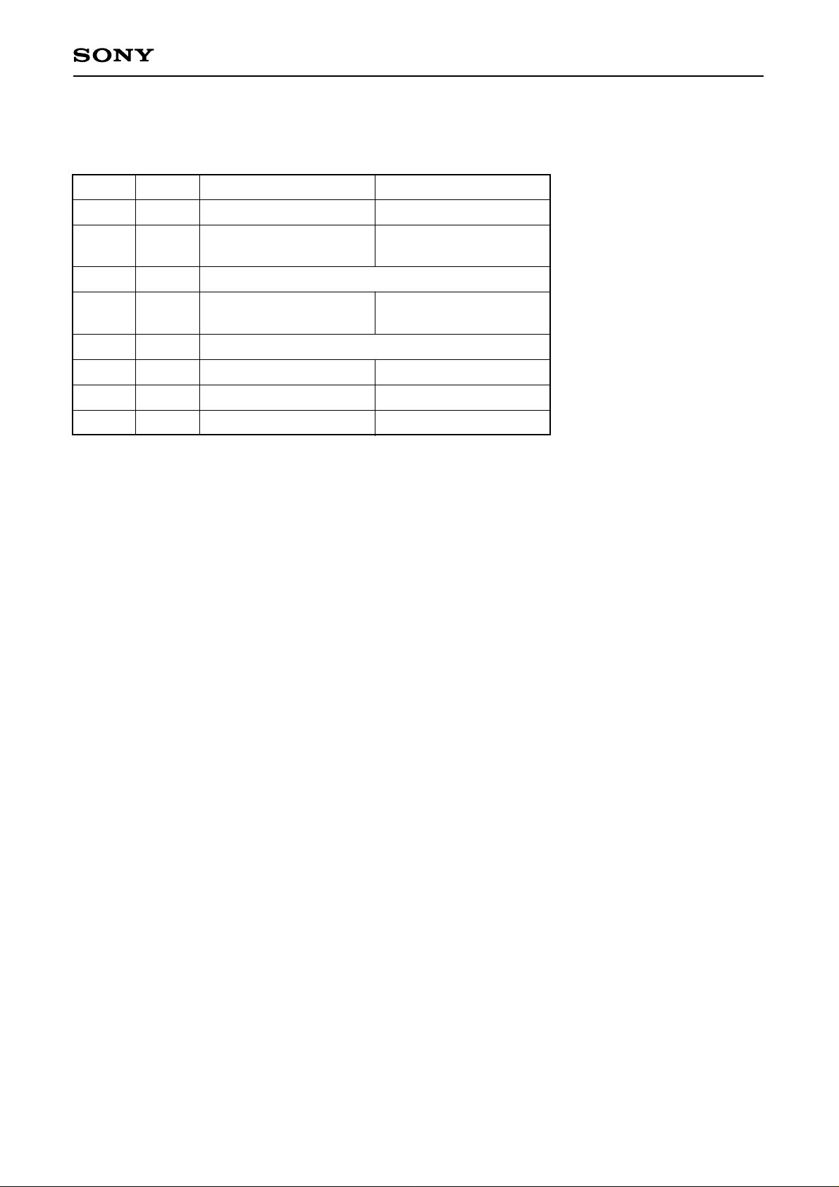
Description of Operation
1. Mode Control
CXD1265R
Symbol
GM
PS
EF
HTSG
D1
D2
D3
D4
∗1
Characteristics of CCD image sensor are guaranteed by field accumulation.
∗2
Operation with GM = High and D2 = High (black-and-white digital signal processing) cannot be used.
Pin No. L H
∗2
∗2
55
58
3
61
11
12
13
14
Analog signal processing Digital signal processing
Serial shutter Parallel shutter
speed setting speed setting
Fix at High in normal operation
XSG1, 2 XSG1, 2
OFF ON
Fix at Low in normal operation
Color Black-and-white
Field readout Frame readout
NTSC/EIA PAL/CCIR
∗1
– 5 –
Page 6
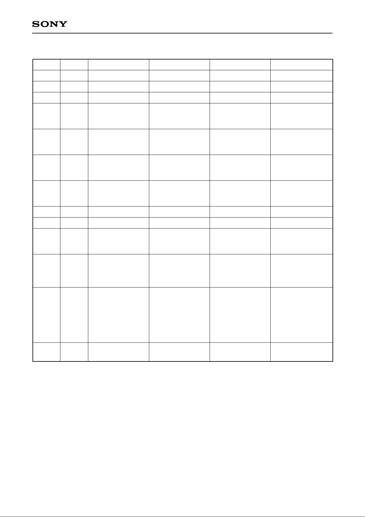
2. Changes in I/O Signals in Each Mode
CXD1265R
Symbol
GM
D2
TEST2
XSP1
XSP2
XSH1
XSH2
XDL1
XDL2
BFG
Pin No. Analog color Digital color 1 Digital color 2 Analog B/W
55
12
36
41
42
43
44
45
46
47
Color separation
sample-and-hold
pulse output
Color separation
sample-and-hold
pulse output
Switching sampleand-hold pulse
output
Switching sampleand-hold pulse
output
Delay line clock
Delay line clock
Burst flag gate
pulse output
L
L
L
H
L
L
H
L
H
L
H
L
Color separation
Halted at High
sample-and-hold
Halted at High
pulse output
Color separation
Halted at High
sample-and-hold
Halted at High
pulse output
Halted at Low
Halted at Low
Halted at High
Halted at Low
Burst flag gate
pulse output
(normally not used)
Switching sampleand-hold pulse
output
Switching sampleand-hold pulse
output
Halted at High
Halted at Low
Burst flag gate
pulse output
(normally not used)
Precharge level
sample-and-hold
pulse output
Data sample-andhold pulse output
Halted at High
Halted at Low
Halted at Low
Standby control input
CLP2
49
Clamp pulse output
Low: Standby
High: Normal
operation
Standby control
∗
Low: All circuits
halted for
CLP3
50
Clamp pulse output
standby mode
High: Only CL
output for
standby mode
ID
∗
When CLP2 = High, normal operation occurs regardless of whether CLP3 is high or low.
53
Line identification
output
Line identification
output
Standby control input
Low: Standby
High: Normal
operation
Standby control
∗
Low: All circuits
halted for
standby mode
High: Only CL
output for
standby mode
Line identification
output
Clamp pulse output
Clamp pulse output
(phase change)
Halted at Low
(Mode combinations other than those shown above cannot be used.)
Note) In the standby mode described above, XCK, XSG1, XSG2, XV1, XV2, XV3, XV4, XSUB, H1, H2, RG,
XSHD, XSHP, XSP1, XSP2, XSH1, XSH2, XDL1, and XDL2 pins are halted at Low. MCK, CLP1, CLP4,
PBLK, ID, XVCT, WEN, BFG, A0, A1, A2, A3, A4, and A5 pins are halted at the state just before
standby.
– 6 –
Page 7
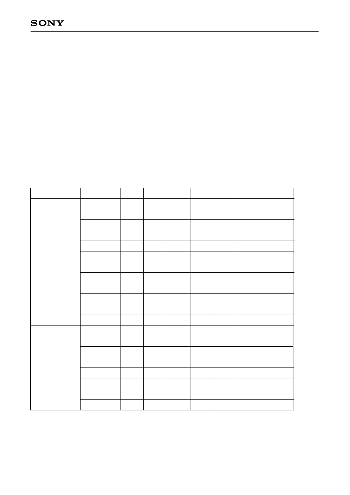
3. Electronic Shutter
<Shutter Modes>
SMD1 SMD2
L L Flickerless: Eliminates fluorescent frequency-induced flicker.
L H High-speed shutter: Shutter speed faster than 1/60 (NTSC), 1/50 (PAL)
H L Low-speed shutter: Shutter speed slower than 1/60 (NTSC), 1/50 (PAL)
H H No shutter operation
<Shutter Mode and Speed Setting Method>
PS = High: Parallel input; set by ED0 to ED2, SMD1, and SMD2.
PS = Low: Serial input; set by inputting ED0 (strobe), ED1 (clock), and ED2 (data) to each pin.
3-1. Parallel input (PS = H)
Shutter Speed Compatibility Chart
CXD1265R
Mode
OFF
Flickerless
High-speed
shutter
Low-speed
shutter
∗
NTSC/PAL
X
NTSC
PAL
NTSC
PAL
X
X
X
X
X
X
X
X
X
X
X
X
SMD1 SMD2 ED0 ED1 ED2 Shutter speed
H
L
L
L
L
L
L
L
L
L
L
L
H
H
H
H
H
H
L
L
H
H
H
H
H
H
H
H
H
L
L
L
L
L
X
X
X
H
H
L
H
L
H
L
H
L
H
L
H
L
H
X
X
X
H
H
H
L
L
H
H
L
L
H
H
L
L
H
X
X
X
H
H
H
H
H
L
L
L
L
H
H
H
H
L
Shutter off
1/100 (S)
1/120 (S)
1/60 (S)
1/50 (S)
1/125 (S)
1/250 (S)
1/500 (S)
1/1000 (S)
1/2000 (S)
1/4000 (S)
1/10000 (S)
2FLD
4FLD
6FLD
8FLD
10FLD
X
X
X
∗
During frame accumulation mode, low speed shutter data set to ED0 to ED2 are all invalid.
H
H
H
L
L
L
L
H
L
H
L
L
L
12FLD
L
14FLD
L
16FLD
Shutter speed is 1/30s for NTSC; 1/25s for PAL.
– 7 –
Page 8

CXD1265R
3-2. serial input (PS=L)
For serial input (PS = L), SMD1 and SMD2 bits within ED2 (DATA) take priority over SMD1 (Pin 7) and SMD2
(Pin 9) pins as SMD1 and SMD2 (shutter mode control).
In this case, control by SMD1 and SMD2 pins is invalid.
ED1 (CLK)
ED2 (DATA)
ED0 (STB)
ED2 data is latched to the register at the rise of ED1, and transferred to the within during the Low period of ED0.
D0 D1
D2 D3 D4 D5 D6 D7 D8 SMD1 SMD2 Dummy
– 8 –
Page 9
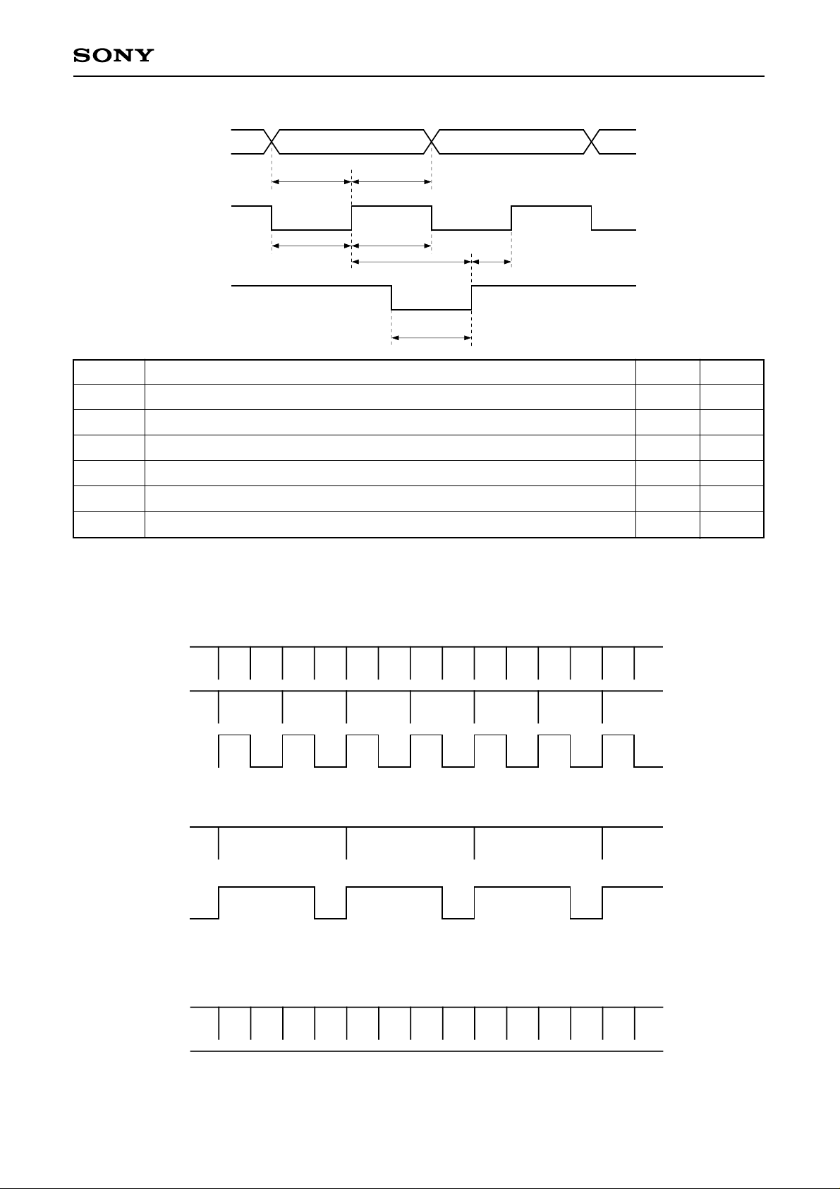
AC Characteristics
CXD1265R
ED2
ts2 th2
ED1
tw1 tw1
ts1 ts0
ED0
tw0
Symbol
tS2
th2
tS1
tW0
tS0
tW1
ED2 set-up time, activated by the rising edge of ED1
ED2 hold time, activated by the rising edge of ED1
ED1 rising set-up time, activated by the rising edge of ED0
ED0 pulse width
ED0 rising set-up time, activated by the rising edge of ED1
ED1 pulse width (serial input)
3-4. Low-speed shutter timing chart
(During field accumulation mode)
OEOEOEOEOEOEOE
VD
XSG1, 2
WEN
Min. Max.
20ns
20ns
20ns
20ns
20ns
20ns
(ED2 : ED1 : ED0 = H : H : H)
—
—
—
50µs
—
—
XSG1, 2
WEN
(During frame accumulation mode)
XSG1, 2
WEN
(Fixed at H)
(ED2 : ED1 : ED0 = H : H : L)
(ED2 : ED1 : ED0 = X : X : X)
– 9 –
Page 10
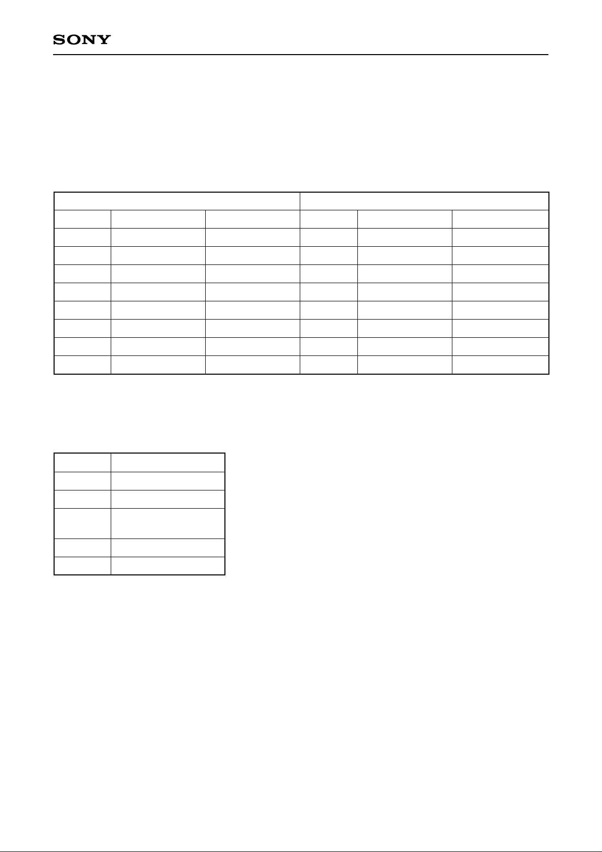
3-5. Shutter speed calculation formula
1. High-speed shutter
• NTSC (L16 = load value)
T = [26210 – (1FF16 – L16) ] × 63.56µs + 34.9µs
• PAL (L16= load value)
T = [31210 – (1FF16 – L16) ] × 64.00µs + 35.0µs
CXD1265R
NTSC
Load value
0FA16
0FC16
10016
10816
11816
13716
17616
19616
Shutter speed Calculated value Load value Shutter speed Calculated value
1/10000
1/4000
1/2000
1/1000
1/500
1/250
1/125
1/100
1/10156
1/4433
1/2084
1/1012
1/499
1/252
1/125
1/100
0C816
0CA16
0CE16
0D616
0E616
10516
14316
14916
2. Low-speed shutter (Valid during field accumulation mode only)
Shutter speed calculation formula
N = 2 × (1FF16 – L16) FLD
However, "FF" cannot be used as the load value.
Load value
1FE16
Shutter speed (FLD)
2
1/10000
1/4000
1/2000
1/1000
1/500
1/250
1/125
1/120
PAL
1/10101
1/4405
1/2070
1/1005
1/495
1/250
1/125
1/120
1FD16
:
:
10116
10016
4
:
:
508
510
– 10 –
Page 11
494
492
3579
1
CXD1265R
10
2468
493
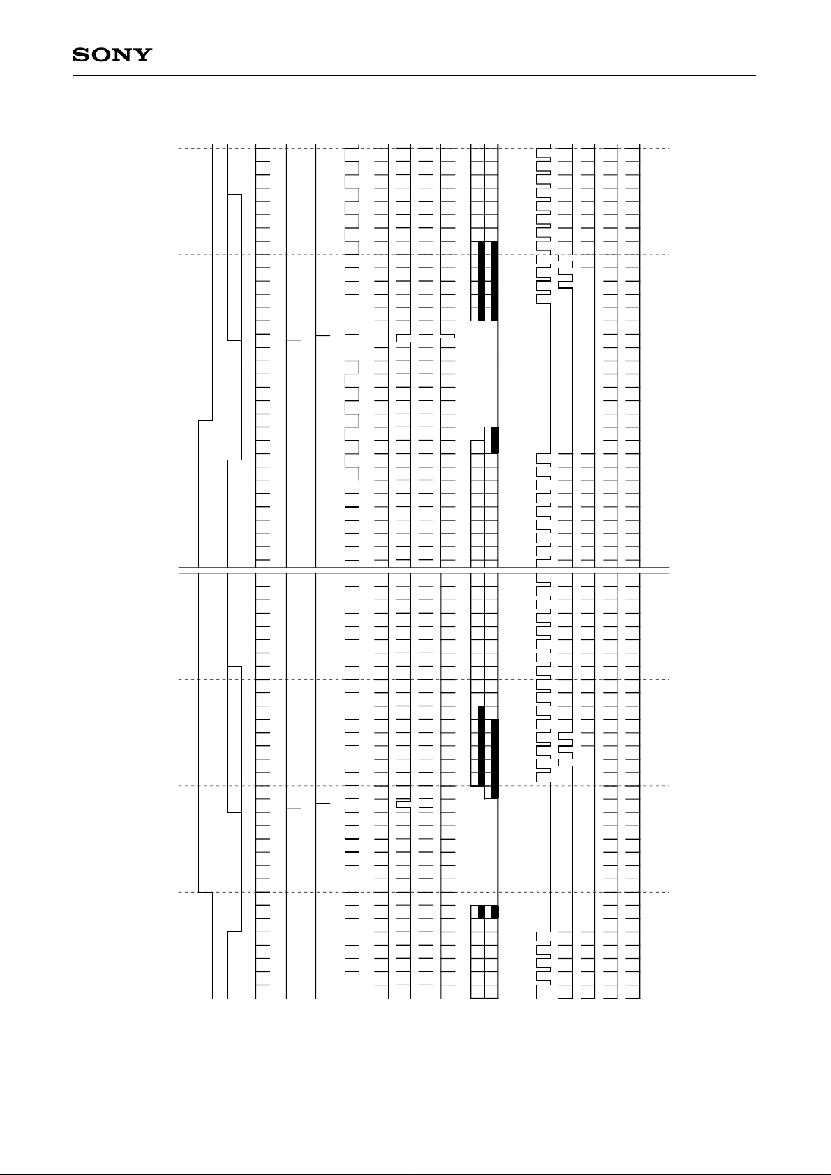
Timing Chart (1)
NTSC vertical direction
FLD
BLK/VD
HD
XSG1
XSG2
3579
2468
1
493
494
However, ID is halted for black-and-white mode
ID
XV1
XV2
XV3
XV4
CCD
PBLK
CLP1
CLP2
CLP3
CLP4
– 11 –
Page 12
3579
1
CXD1265R
10
2468
582
2468
3579
1
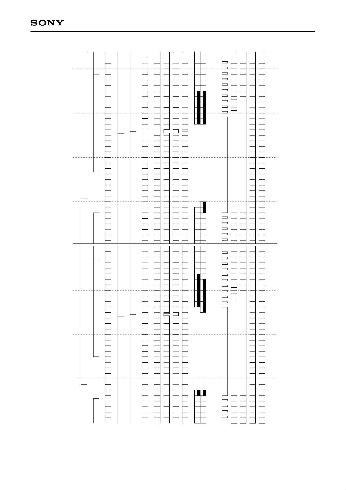
Timing Chart (2)
PAL vertical direction
FLD
BLK/VD
HD
XSG1
XSG2
582
581
ID
XV1
XV2
XV3
XV4
CCD
PBLK
CLP1
CLP2
CLP3
CLP4
However, ID is halted for black-and-white mode
– 12 –
Page 13

160 170 180
155
140
140
CXD1265R
140
130 140 150
120
135
113
103
96
98
89
80
80
71
62
53
114
86
81
75
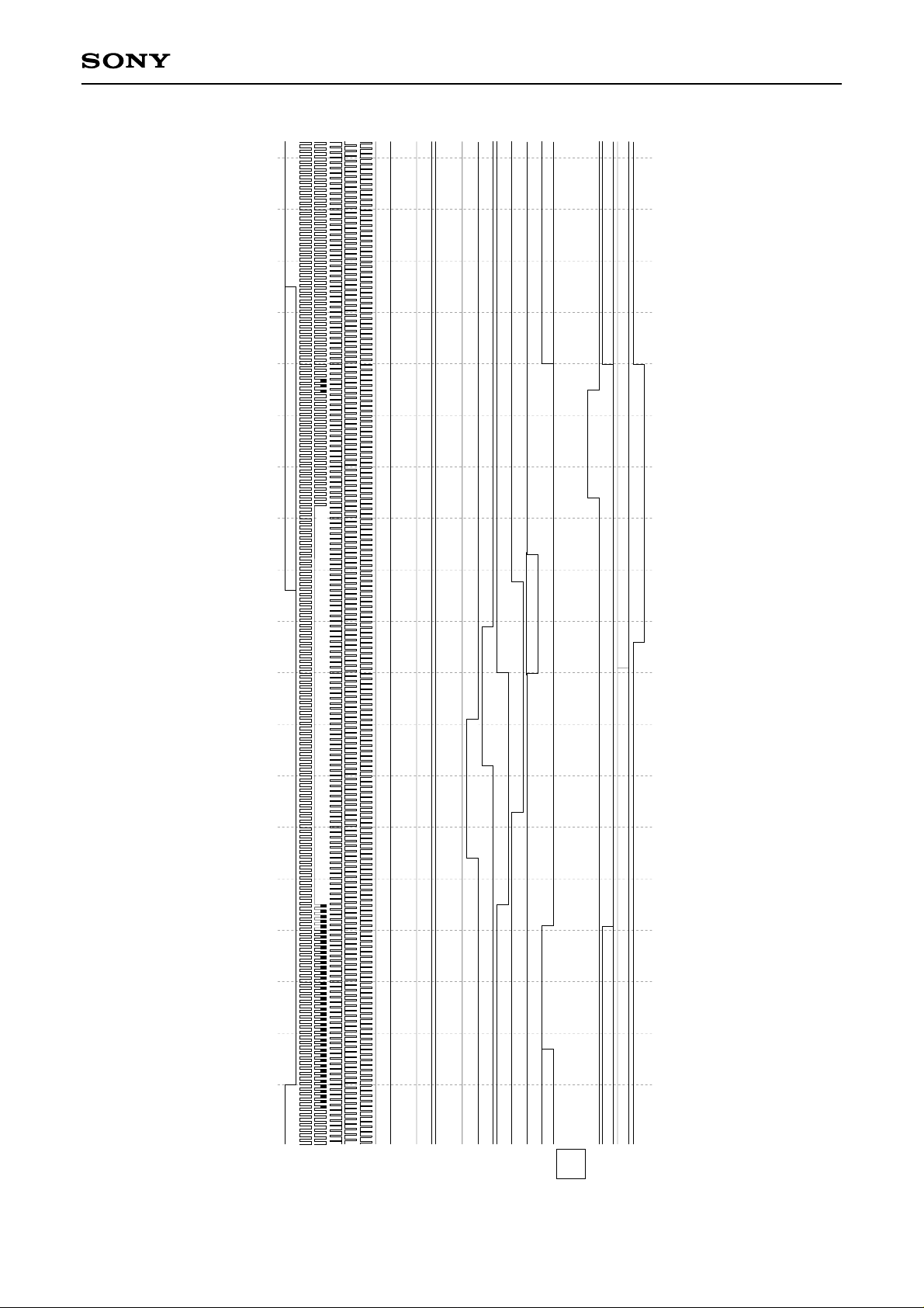
Black painted portions indicate the optical black output timing of CCD.
51
35
0 10 20 30 40 50 60 70 80 90 100 110
CL
H1
RG
BLK/HD
Timing Chart (3)
NTSC horizontal direction, analog color
XSHP
XSHD
XSP1
XSP2
XSH1
XDL1
XSH2
– 13 –
XDL2
44
XV1
XV2
35
XV3
XV4
XSUB
31
7
CLP1
38
14
CLP2
CLP3
CLP4
31
PBLK
ID
BFG
(GM = L, D2=L, TEST2 = L)
Page 14
160 170 180
CXD1265R
155
130 140 150
120
114
135
140
140
86
81
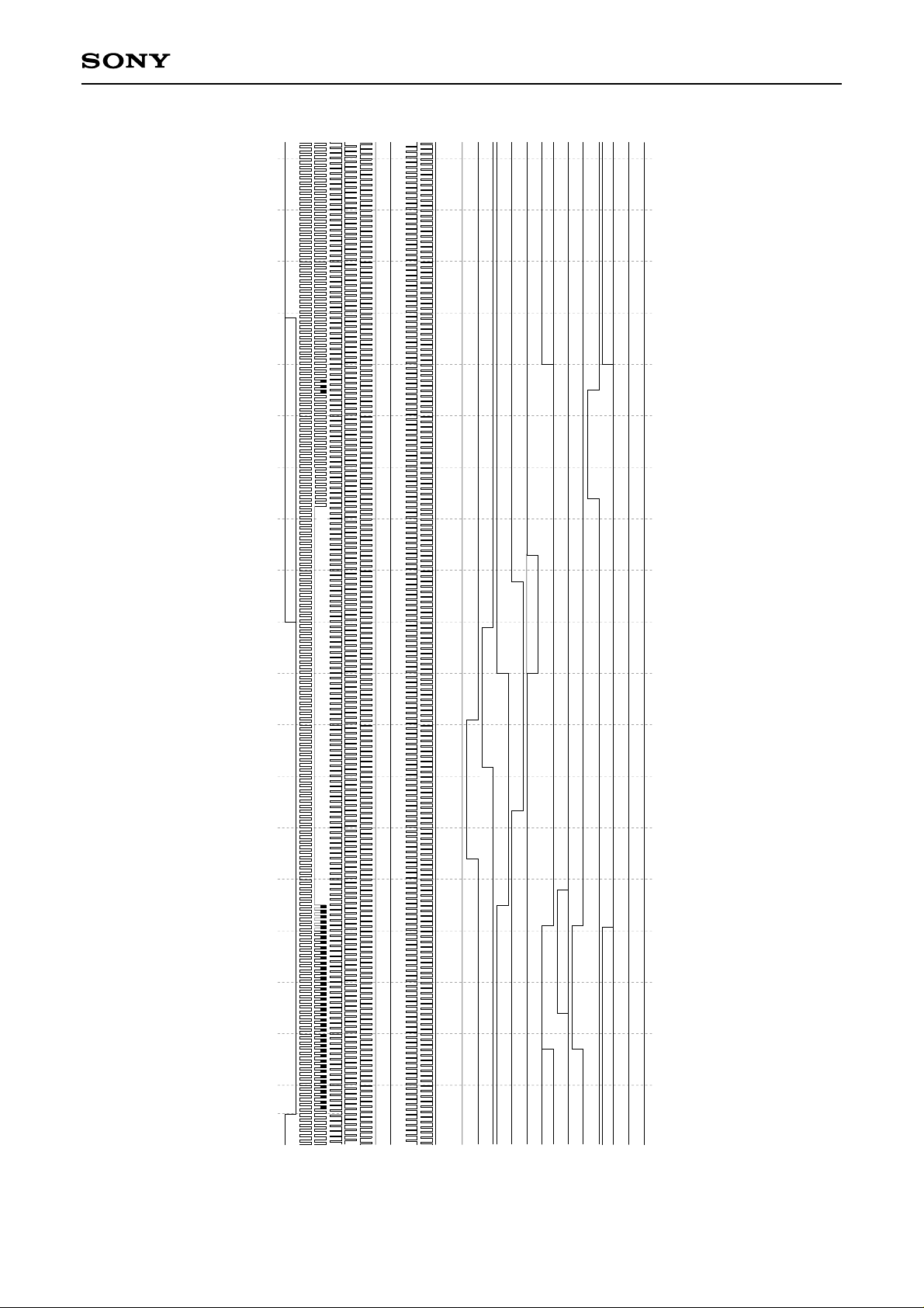
Black painted portions indicate the optical black output timing of CCD.
140
113
103
96
98
89
80
80
71
62
53
35
10 20 30 40 50 60 70 80 90 100 110
0
CL
H1
RG
BLK/HD
Timing Chart (4)
NTSC horizontal direction, digital color 1
XSHP
XSHD
H
XSP1
H
XSP2
L
XSH1
L
H
XDL1
XSH2
– 14 –
L
XDL2
44
XV1
XV2
35
XV3
XV4
XSUB
31
7
CLP1
INPUT PIN
CLP2
CLP3
CLP4
31
PBLK
ID
(GM = H, D2 = L, TEST2 = L)
BFG
Page 15

160 170 180
130 140 150
120
155
140
135
140
CXD1265R
140
113
103
96
35
98
89
80
80
71
62
53
44
35
114
86
81
Black painted portions indicate the optical black output timing of CCD.
31
31
0 10 20 30 40 50 60 70 80 90 100 110
CL
H1
RG
BLK/HD
Timing Chart (5)
NTSC horizontal direction, digital color 2
XSHP
XSHD
XSP1
XSP2
XSH1
H
XDL1
XSH2
– 15 –
L
XDL2
XV1
XV2
XV3
XV4
XSUB
7
CLP1
INPUT PIN
CLP2
CLP3
CLP4
PBLK
ID
BFG
(GM = H, D2 = L, TEST2 = H)
Page 16
160 170 180
CXD1265R
149
130 140 150
120
113
140
103
98
89
80
80
71
62
53
140
135
114
Black painted portions indicate the optical black output timing of CCD.
35
10 20 30 40 50 60 70 80 90 100 110
0
–6
CL
H1
BLK/HD
Timing Chart (6)
EIA horizontal direction, analog black-and-white
H
H
RG
XSP1
XSP2
XSHP
XSHD
XSH1
H
XDL1
XSH2
– 16 –
L
XDL2
44
XV1
XV2
35
XV3
XV4
XSUB
31
7
CLP1
38
14
CLP2
31
7
CLP3
CLP4
31
PBLK
L
L
ID
BFG
(GM = L, D2 = H, TEST2 = L)
Page 17
130 140 150 160 170 180
154
149
154
CXD1265R
154
120
126
117
112
101
96
90
90
79
68
128
86
81
75
Black painted portions indicate the optical black output timing of CCD.
57
51
46
35
0 10 20 30 40 50 60 70 80 90 100 110
CL
H1
BLK/HD
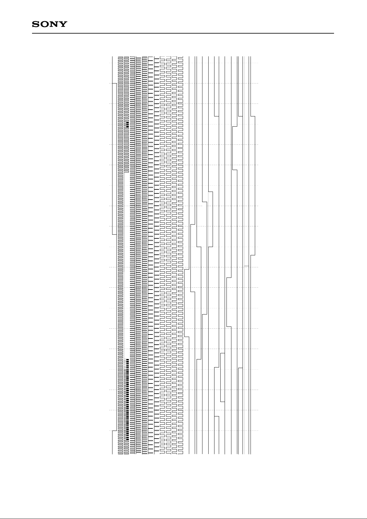
Timing Chart (7)
PAL horizontal direction, analog color
XV4
XSUB
31
7
CLP1
38
14
CLP2
CLP3
CLP4
31
PBLK
ID
BFG
(GM = L, D2 = L, TEST2 = L)
35
RG
XSHP
XSHD
XSP1
XSP2
XSH1
XSH2
XDL1
XDL2
XV1
XV2
XV3
– 17 –
Page 18
130 140 150 160 170 180
154
149
154
CXD1265R
154
120
126
117
112
101
96
90
90
79
68
128
86
81
Black painted portions indicate the optical black output timing of CCD.
57
46
35
10 20 30 40 50 60 70 80 90 100 110
0
CL
H1
RG
BLK/HD
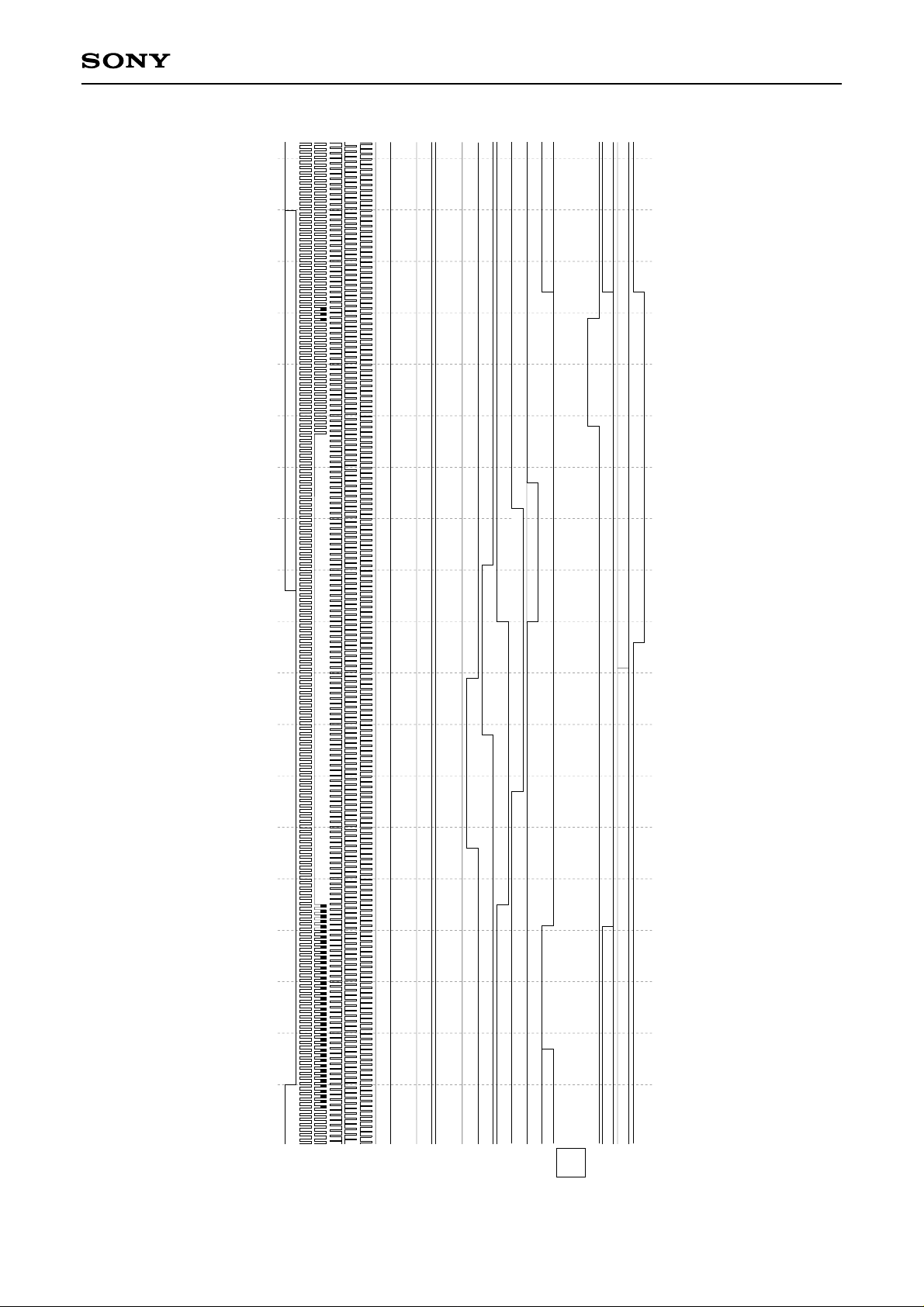
Timing Chart (8)
PAL horizontal direction, digital color 1
XSHP
XSHD
H
XSP1
H
XSP2
L
XSH1
L
H
XDL1
XSH2
– 18 –
L
XDL2
XV1
XV2
35
XV3
XV4
XSUB
31
7
CLP1
INPUT PIN
CLP2
CLP3
CLP4
31
PBLK
ID
BFG
(GM = H, D2 = L, TEST2 = L)
Page 19
130 140 150 160 170 180
154
149
154
CXD1265R
154
120
126
117
112
101
96
90
90
79
68
128
86
81
Black painted portions indicate the optical black output timing of CCD.
57
46
35
0 10 20 30 40 50 60 70 80 90 100 110
CL
H1
RG
BLK/HD
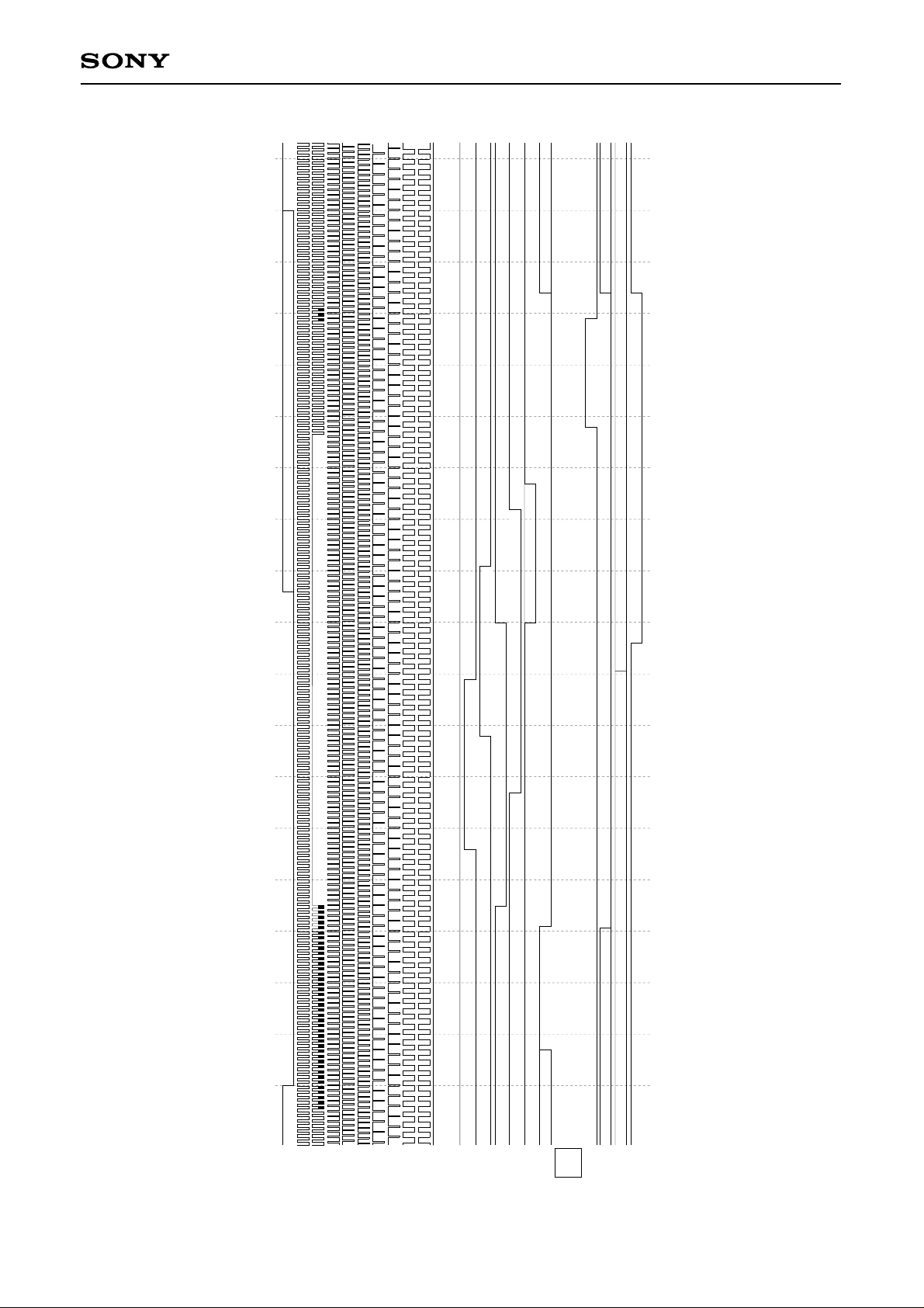
Timing Chart (9)
PAL horizontal direction, digital color 2
XSHP
XSHD
XSP1
XSP2
XSH1
H
XDL1
XSH2
– 19 –
L
XDL2
XV1
XV2
35
XV3
XV4
XSUB
31
7
CLP1
INPUT PIN
CLP2
CLP3
CLP4
31
PBLK
ID
BFG
(GM = H, D2 = L, TEST2 = H)
Page 20

160 170 180
CXD1265R
164
130 140 150
120
126
154
117
112
101
90
90
79
68
154
149
128
35
10 20 30 40 50 60 70 80 90 100 110
0
–6
CL
H1
BLK/HD
Timing Chart (10)
CCIR horizontal direction, analog black-and-white
H
H
RG
XSP1
XSP2
XSHD
XSH1
XSHP
XSH2
H
XDL1
L
XDL2
46
XV1
XV2
35
XV3
57
XV4
XSUB
31
7
CLP1
38
14
CLP2
31
7
CLP3
CLP4
31
PBLK
Black painted portions indicate the optical black output timing of CCD.
L
L
ID
BFG
(GM = L, D2 = H, TEST2 = L)
– 20 –
Page 21
CXD1265R
3
578
36
36 36
36
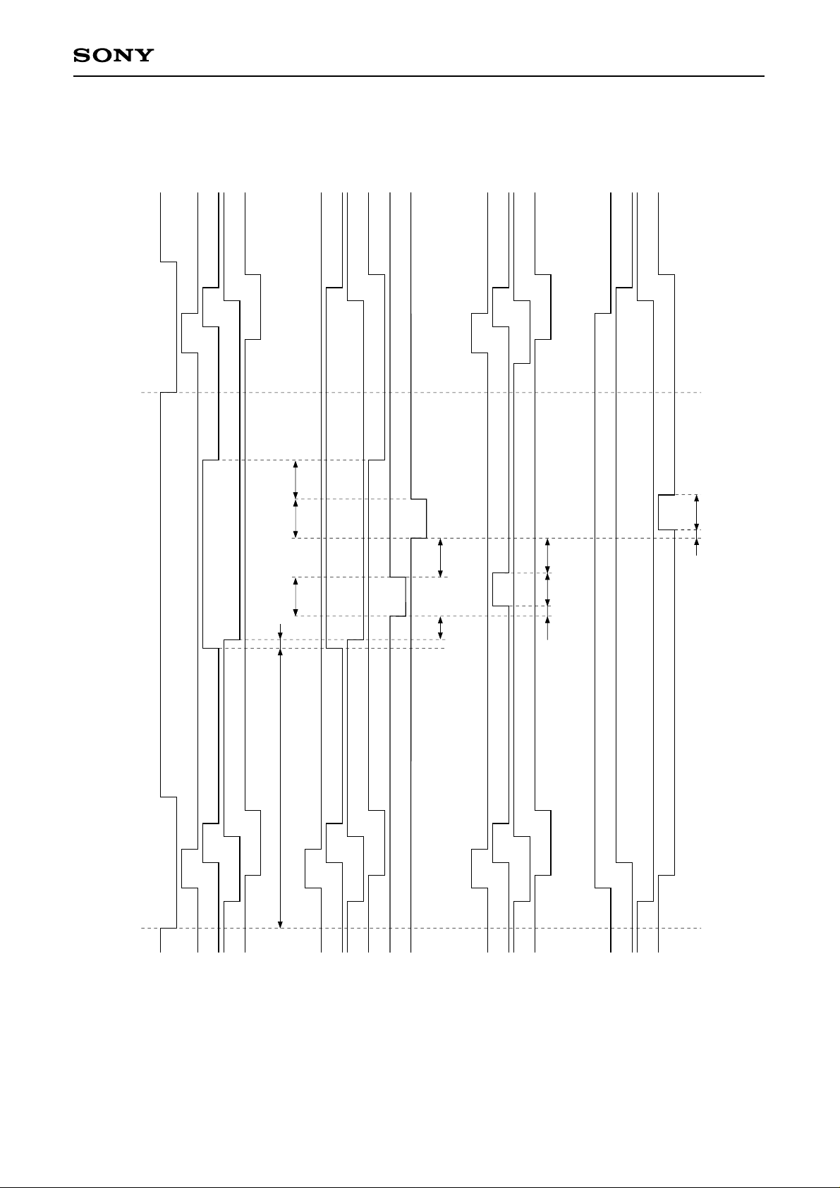
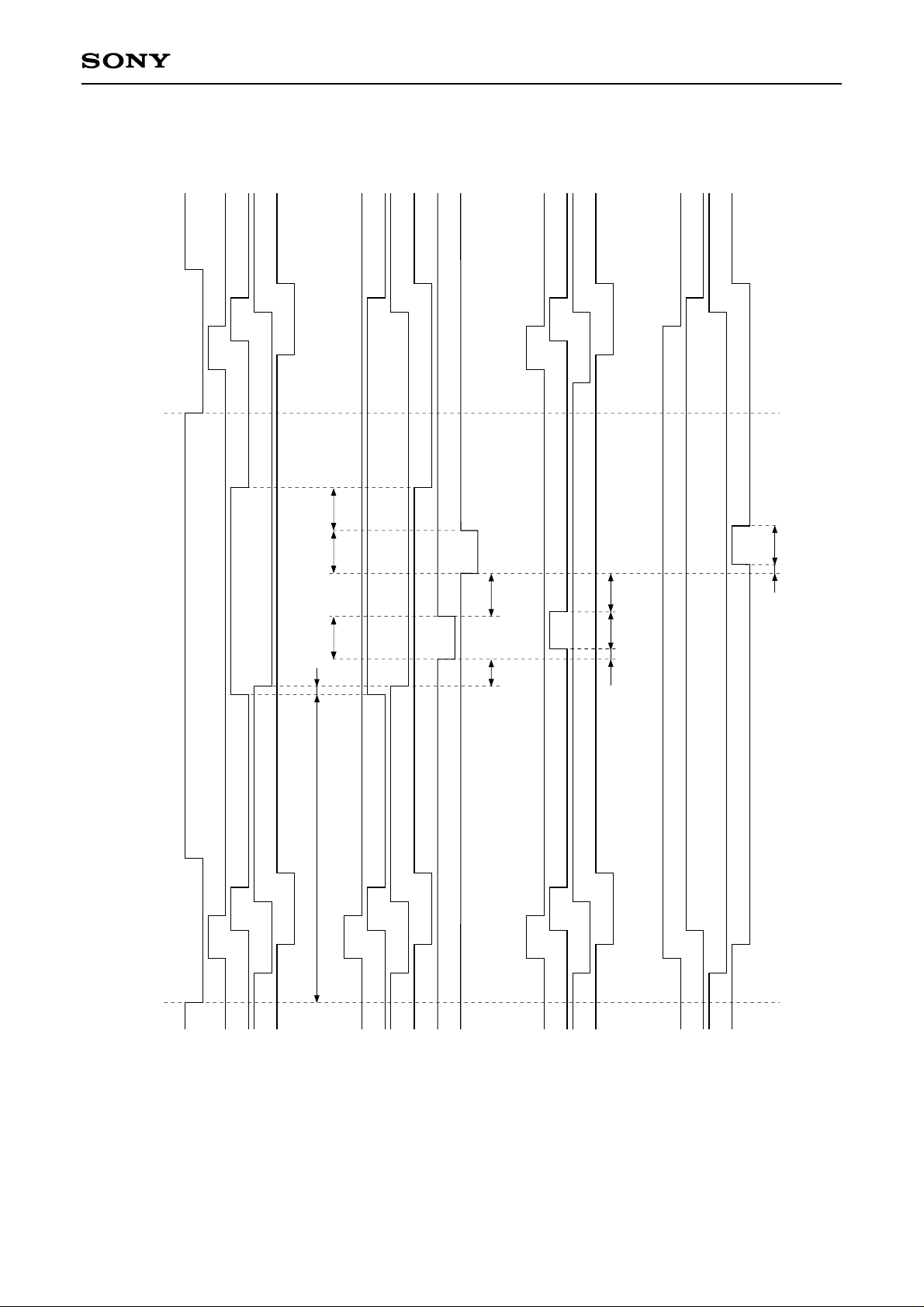
Unit: Number of clocks (1ck = 69.84ns)
36
3
33
36
3
22
HD
XV2
XV3
Field readout
XV1
XV4
ODD
XV1
XV2
4-1. Timing Chart of Readout (NTSC/EIA)
XV3
EVEN
XV4
XSG1
XSG2
– 21 –
XV2
XV1
ODD
Frame readout
XV3
XV4
XV1
XV2
EVEN
XV3
XV4
Page 22
CXD1265R
3
589
36
36 36
36
Unit: Number of clocks (1ck = 70.48ns)
36
3
33
36
3
22
HD
XV2
XV3
XV1
ODD
Field readout
XV4
XV1
4-2. Timing Chart of Readout (PAL/CCIR)
XV2
XV3
EVEN
XV4
– 22 –
XSG1
XSG2
Frame readout
XV1
XV2
ODD
XV3
XV4
XV1
XV2
XV3
EVEN
XV4
Page 23
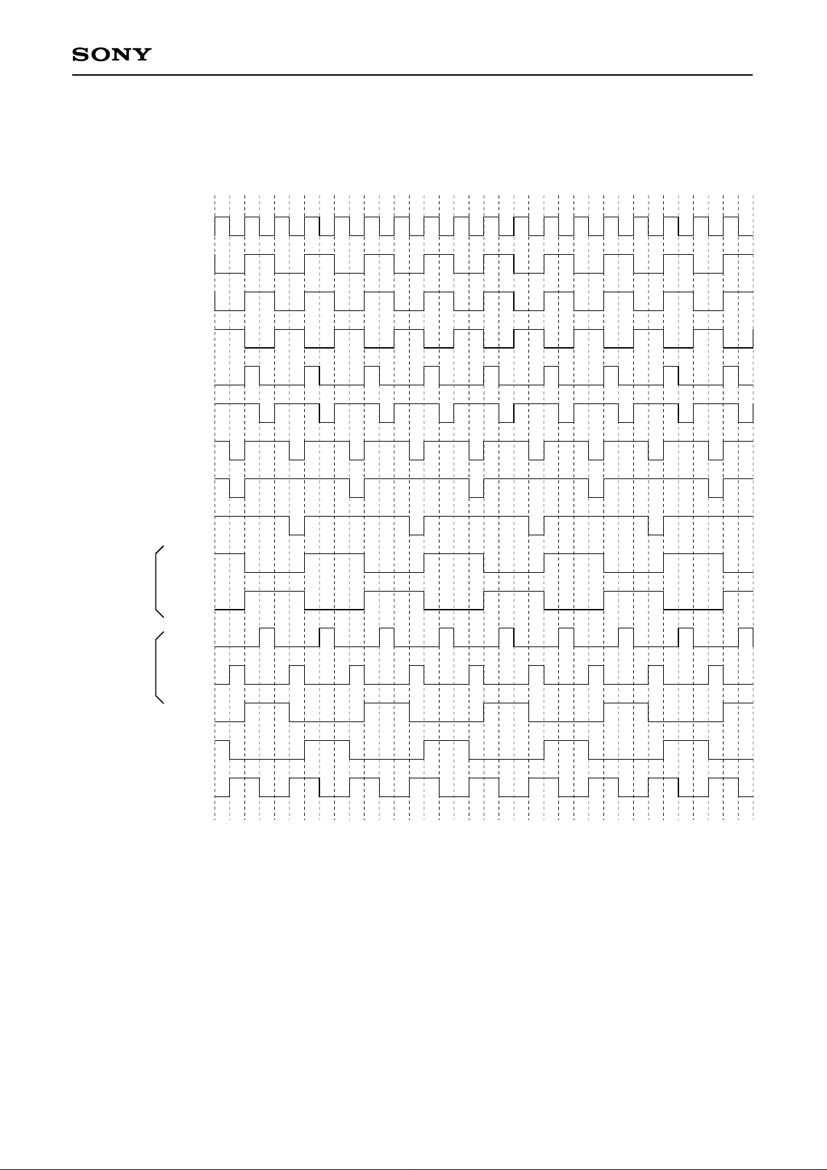
5. High-speed Clock Timing Chart
CK
CL
H1
H2
RG
XSHP
XSHD
XSP1
CXD1265R
For color mode
For
black-and-white
mode
XSP2
XSH1
XSH2
XSH1
(SHP)
XSH2
(SHD)
XDL1
XDL2
MCK
∗
For black and white mode, XSP1, XSP2, XDL1, and XDL2 are halted.
– 23 –
Page 24
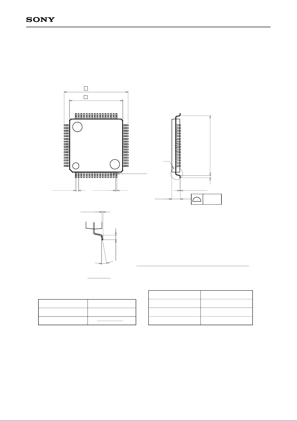
Package Outline Unit: mm
12.0 ± 0.2
∗ 10.0 ± 0.1
CXD1265R
64PIN LQFP (PLASTIC)
49
64
0.5 ± 0.08
48
1
0.18 – 0.03
0.1 ± 0.1
+ 0.08
33
16
32
17
(0.22)
A
+ 0.2
1.5 – 0.1
(11.0)
0.5 ± 0.2
+ 0.05
0.127 – 0.02
0.1
SONY CODE
EIAJ CODE
JEDEC CODE
0° to 10°
DETAIL A
0.5 ± 0.2
LQFP-64P-L01
∗QFP064-P-1010-A
NOTE: Dimension “∗” does not include mold protrusion.
PACKAGE STRUCTURE
PACKAGE MATERIAL
LEAD TREATMENT
LEAD MATERIAL
PACKAGE WEIGHT
– 24 –
EPOXY / PHENOL RESIN
SOLDER PLATING
42 ALLOY
0.3g
 Loading...