

Page 1

CXD1254AR/AQ
CCD Camera Synchronization and Timing Signal Generator
Description
The CXD1254AR and CXD1254AQ Ics generates
the necessary synchronization and timing signals for
camera systems employing CCD image sensors
(ICX044, ICX045, ICX046, etc.).
Features
• Supports color (NTSC) and black & white
(EIA/CCIR) systems
• On-chip electronic shutter
• On-chip horizontal (H) driver
• Timing generator for mirror images
Applications
CCD camera systems
CXD1254AR CXD1254AQ
64 pin LQFP (Plastic) 64 pin QFP (Plastic)
Absolute Maximum Ratings (Ta=25 °C, VSS=0 V)
• Supply voltage VSS –0.5 to +7.0 V
• Input voltage VSS –0.5 to VDD +0.5 V
• Output voltage VSS –0.5 to VDD +0.5 V
• Operating temperature –20 to +75 °C
• Storage temperature –55 to +150 °C
Structure
Silicon gate CMOS IC
Recommended Operating Conditions
• Supply voltage 4.75 to 5.25 V
• Operating temperature –20 to +75 °C
Sony reserves the right to change products and specifications without prior notice. This information does not convey any license by
any implication or otherwise under any patents or other right. Application circuits shown, if any, are typical examples illustrating the
operation of the devices. Sony cannot assume responsibility for any problems arising out of the use of these circuits.
—1—
E91845B67-TE
Page 2

Block Diagram (Pin No.s given for CXD1254AR)
TEST2
54
TEST3
58
GENERATOR
TEST
52
EXT
48
TEST1
FLD
49
GENERATOR
RESET
1/7 or 1/6
COUNTER
1/65 COUNTER
H-DECODER
1/525 or 1/625
COUNTER
V-DECODER
V-CONTROL
CXD1254AR/AQ
4
D1
5
D2
6
D3
HD
VD
C KIN
OSCI
OSCO
PS
ED0
ED1
ED2
ENB
OUTPUT CONTROL
1
2
H-INIT
V-INIT
11
1/3
9
1/2
10
3
CL
RESET
CK
GENERATION
PHASE CONT.
16
13
14
15
12
V-RELATIVE
COUNTER
V-ROM
(VD1)
LATCH
CONVERTER
PARALLEL
SERIAL-
SELECT
SHUTTER
ROM
H-RELATIVE COUNTER
LATCH
H-ROM
(HD1)
H-ROM
(HD2)
LATCH LATCH LATCH
GATE
COUNTER/GATE
ADDRESS
COUNTER
H-ROM
(HD3)
GATE GATEGATE
LATCH
H-ROM
(RD1)
H-RELATIVE COUNTER
ADDRESS
COUNTER
H-ROM
(RD2)
BF
62
63
CBLK
64
SYNC
XDL1
XDL2
41 4342 44
H2
H3
H1
H4
XSHP
XSHD
XSP1
XSP2
RG
XSUB
PBLK
BFG
ID
CLP2
CLP1
27 2926 3121 233334 35 3618 2037 38 19 25 3945 46 28 30
XV1
XV2
CLP4
CLP3
XV3
XV4
XSG1
XSG2
—2—
Page 3
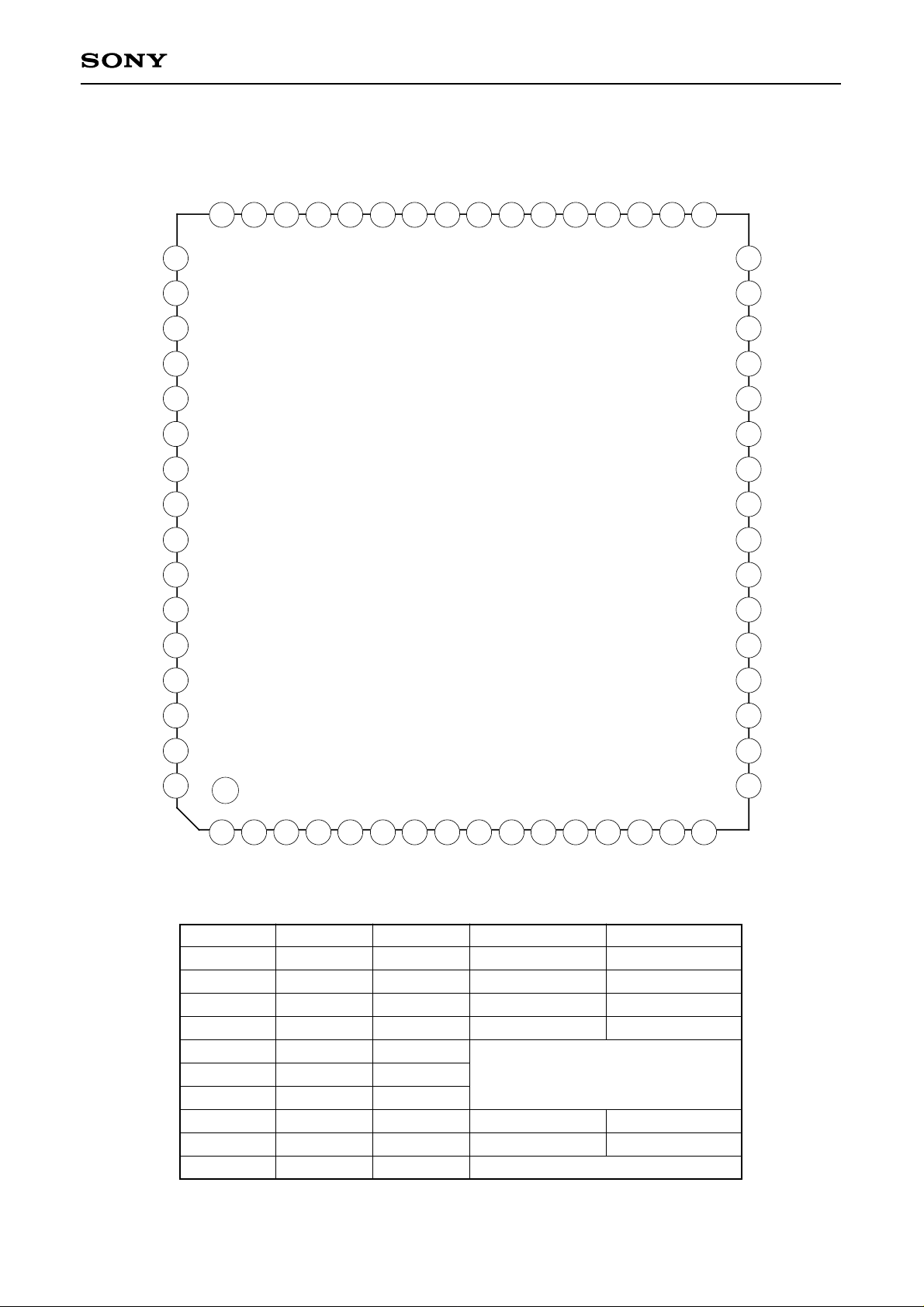
Pin Configuration (1)
CXD1254AR/AQ
FLD
HTSG
DD
V
EXT
SS
V
TEST2
NC
DD
V
NC
TEST3
SS
V
49
50
51
52
53
54
55
56
57
58
59
TEST1
DD
V
SS
CLP4
CLP3
ID
PBLK
CLP2
CXD1254AR
CLP1
V
BFG
XDL2
XDL1
XSP2
XSP1
XSHD
33343536373839404142434445464748
XSHP
32
31
30
29
28
27
26
25
24
23
22
SS
V
XV4
XSG2
XV3
XSG1
XV1
XV2
XSUB
DD
V
RG
SS
AV
NC
NC
BF
CBLK
SYNC
60
61
62
63
64 17
21
20
19
18
1 2 3 4 5 6 7 8 9 10 11 12 13 14 15 16
TRIG
SS
V
OSCI
OSCO
CKIN
ENB
ED0
Low High
NTSC/EIA CCIR
Normal Image Mirror Image
Color B/W
Normal Shutter
Shutter Speed
Serial input Parallel input
Internal External
Normally Low
ED1
ED2
PS
Mode
D1
D2
D3
ENB
ED0
ED1
ED2
PS
EXT
TEST2
HD
VD
CL
Pin No.
4
5
6
12
13
14
15
16
52
54
D1
D2
D3
PRESET
Low
Low
Low
High
High
High
High
High
Low
Low
H4
H3
H2
H1
AV
DD
—3—
Page 4

Pin Configuration (2)
CXD1254AR/AQ
HTSG
V
EXT
V
TEST2
NC
V
NC
TEST3
V
NC
NC
DD
SS
DD
SS
52
53
54
55
56
57
58
59
60
61
62
63
FLD
TEST1
DD
V
PBLK
CLP4
CLP3
ID
CLP2
SS
V
CLP1
CXD1254AQ
BFG
XDL2
XDL1
XSP2
XSP1
XSHD
XSHP
SS
V
XV4
33343536373839404142434445464748495051
32
XSG2
31
XV3
30
XSG1
29
XV1
28
XV2
27
XSUB
26
DD
V
25
RG
24
SS
AV
23
H4
22
H3
21
H2
BF
64
1 2 3 4 5 6 7 8 9 10 11 12 13 14 15 16 17 18 19
CBLK
SYNC
Mode
D1
D2
D3
ENB
ED0
ED1
ED2
PS
EXT
TEST2
HD
VD
CL
Pin No.
6
7
8
14
15
16
17
18
54
56
D1
D2
D3
PRESET
Low
Low
Low
High
High
High
High
High
Low
Low
TRIG
SS
V
OSCI
OSCO
CKIN
ENB
ED0
ED1
Low High
NTSC/EIA CCIR
Normal Image Mirror Image
Color B/W
Normal Shutter
Shutter Speed
Serial input Parallel input
Internal External
Normally Low
ED2
PS
DD
AV
20
H1
—4—
Page 5
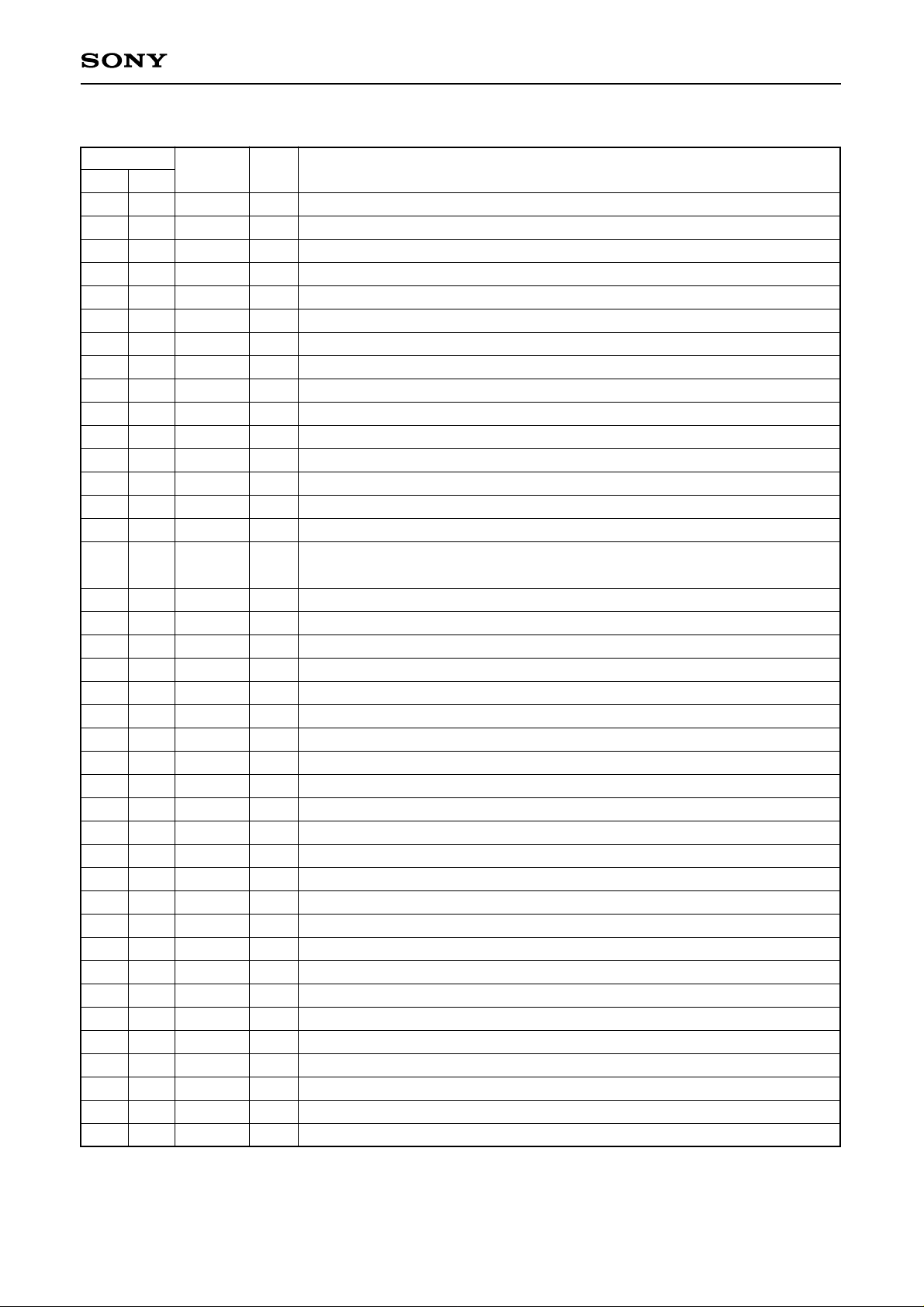
Pin Description
CXD1254AR/AQ
Pin No.
LQFP QFP
13
24
35
46
57
68
79
810
911
10 12
11 13
12 14
13 15
14 16
15 17
16 18
17 19
18 20
19 21
20 22
21 23
22 24
23 25
24 26
25 27
26 28
27 29
28 30
29 31
30 32
31 33
32 34
33 35
34 36
35 37
36 38
37 39
38 40
39 41
40 42
Pin
HD
VD
CL
D1
D2
D3
TRIG
VSS
OSCI
OSCO
CKIN
ENB
ED0
ED1
ED2
PS
AVDD
H1
H2
H3
H4
AVSS
RG
VDD
XSUB
XV2
XV1
XSG1
XV3
XSG2
XV4
VSS
XSHP
XSHD
XSP1
XSP2
XDL1
XDL2
BFG
VSS
I/O
O
Horizontal drive pulse output
O
Vertical drive pulse output
O
Clock output NTSC/EIA: 14.318 MHz CCIR: 14.1875 MHz
I
Mode selection “Low”: NTSC/EIA “High”: CCIR (Pull-down resistor)
I
Mode selection “Low”: Normal “High”: Mirror (Pull-down resistor)
I
Mode selection “Low”: Color “High”: B/W (Pull-down resistor)
I
Shutter speed setting pulse input (Pull-up resistor)
—
GND for signal generator
I
Oscillator input NTSC/EIA: 28.636 MHz CCIR: 28.375 MHz
O
Oscillator output
I
Input for determining oscillator duty cycle
I
Shutter selection “Low”: Normal “High”: Shutter (Pull-up resistor)
I
Shutter speed control (Pull-up resistor)
I
Shutter speed control (Pull-up resistor)
I
Shutter speed control (Pull-up resistor)
Shutter speed setting data format selection
I
—
Independent power supply for horizontal driver
O
Clock output for horizontal register driver
O
Clock output for horizontal register driver (Leave open except for ICX046.)
O
Clock output for horizontal register driver (Use as H2 except for ICX046.)
O
Clock output for horizontal register driver (Leave open except for ICX046.)
—
Independent GND for horizontal driver
O
Reset gate pulse output
—
Power supply for timing generator
O
Sensor charge sweep output pulse output
O
Clock output for vertical register driver
O
Clock output for vertical register driver
O
Sensor charge readout pulse output
O
Clock output for vertical register driver
O
Sensor charge readout pulse output
O
Clock output for vertical register driver
O
GND for timing generator
Pre-charge level/sample-and-hold pulse output
O
Data sample-and-hold pulse output
O
Color separation sample-and-hold pulse output
O
Color separation sample-and-hold pulse output
O
Pulse output for delay line
O
Pulse output for delay line
O
O
Burst flag gate pulse output
—
GND for timing generator
“Low”: Serial “High”: Parallel (Pull-up resistor)
Function
∗
1
∗
1
∗
1
∗
1
∗
1
∗
1
—5—
Page 6
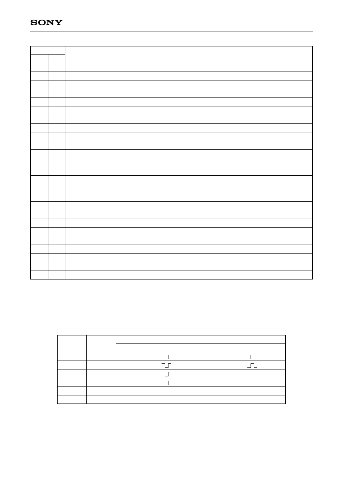
CXD1254AR/AQ
Pin No.
LQFP QFP
41 43
42 44
43 45
44 46
45 47
46 48
47 49
48 50
49 51
50 52
51 53
52 54
53 55
54 56
55 57
56 58
57 59
58 60
59 61
60 62
61 63
62 64
63 1
64 2
Pin
CLP1
CLP2
CLP3
CLP4
PBLK
ID
VDD
TEST1
FLD
HTSG
VDD
EXT
VSS
TEST2
NC
VDD
NC
TEST3
VSS
NC
NC
BF
CBLK
SYNC
I/O
O
Pulse output for clamp
O
Pulse output for clamp
O
Pulse output for clamp
O
Pulse output for clamp
O
Blanking/cleaning pulse output
O
Line discrimination pulse output
—
Power supply for timing generator
I
Test input/H reset pulse input
I/O
Field pulse output/V reset pulse input
I
XSG1, 2 controller/Test input
—
Power supply for signal generator
Synchronization mode selection.
I
—
GND for signal generator
I
Test input (Normally open) (Pull-down resistor)
—
Used open
—
Power supply for signal generator
—
Used open
I
Test input (Normally fixed at “Low”)
—
GND for signal generator
—
Used open
—
Used open
O
Burst flag pulse output
O
Composite blanking pulse output
O
Composite synchronization pulse output
(Note)∗1…Output determined by mode setting.
∗
2…Function determined by mode setting.
Function
∗
∗
∗
“Low”: Internal “High”: External (Pull-down resistor)
2
2
2
Outputs for Pins Determined by Mode Setting
∗
1
Pin
XSHP
XSHD
XSP1
XSP2
XDL1
XDL2
Pin No.
(LQFP)
33
34
35
36
37
38
Low (Color) High (B/W)
O
O
O
O
XSHP ( ) output
XSHD ( ) output
XSP1 ( ) output
XSP2 ( ) output
O
O
XDL1 output
XDL2 output
—6—
D3 (Pin 6)
O
O
O
O
O
O
SHP ( ) output
SHD ( ) output
(Out put stopped)
(Out put stopped)
(Out put stopped)
(Out put stopped)
Page 7
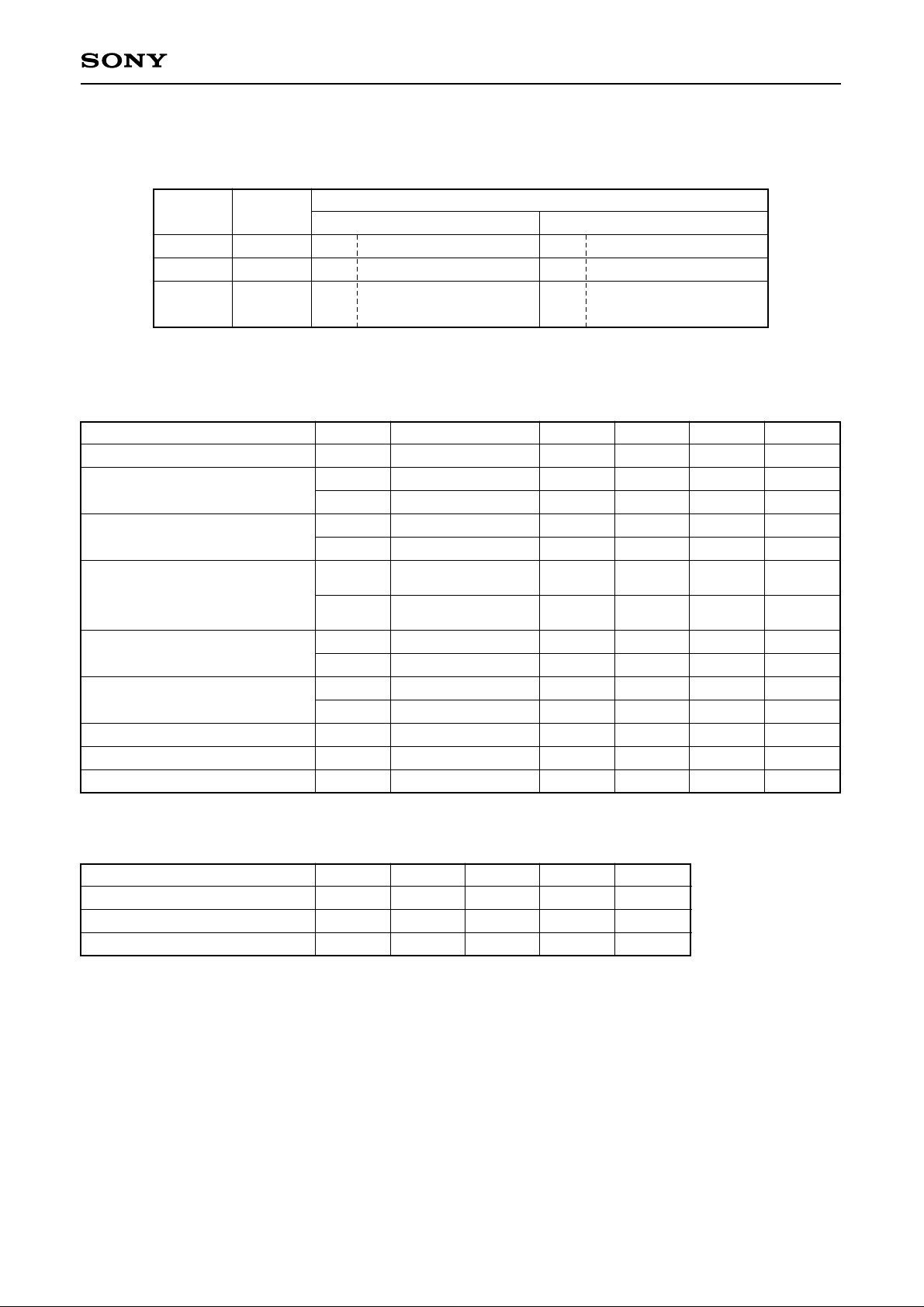
CXD1254AR/AQ
Functions for Pins Determined by Mode Settings
∗
2
Pin
TEST1
FLD
HTSG
Pin No.
(LQFP)
48
49
50
Low (Internal) High (External)
Test input (Normally low)
I
O
I
(“Low” : OFF “High” : ON)
FLD output
XSG1, 2 control input
EXT (Pin 11)
I
I
I
H reset pulse input
V reset pulse input
Test input (Normally low)
Electrical Characteristics
1) DC Characteristics (VDD=5 V ±0.25 V, Topr= –20 to +75 °C)
Item
Supply voltage
Input voltage
Output voltage 1
Output voltage 2
Symbol
VDD
VIH1
VIL1
VOH1
VOL1
VOH2
Conditions
IOH=–2 mA
IOL=4 mA
IOH=–4 mA
Min.
4.75
0.7 VDD
VDD–0.5
VDD–0.5
Typ.
5.0
CL, RG, XSHP, XSHD, XSP1,
XSP2, XDL1, XDL2
Output voltage 3
H1, H2, H3, H4
Output voltage 4
OSC0
Feedback resistance
Pull-up resistor
Pull-down resistor
VOL2
VOH3
VOL3
VOH4
VOL4
RFB
RPU
RPD
IOL=8 mA
IOH=–8 mA
IOL=8 mA
IOH=–1 mA
IOL=1 mA
VIN=VSS or VDD
VIL=0 V
VIH=VDD
VDD–0.5
VDD/2
500 k
40 k
40 k
2 M
100 k
100 k
2) Input/Output Capacitance (VDD=VI=0 V, fM=1 MHz)
Item
Input pin capacitance
Output pin capacitance
Input/Output pin capacitance
Symbol
CIN
COUT
CI/O
Min. Typ. Max.
9
11
11
Unit
pF
pF
pF
Max.
5.25
0.3 VDD
0.4
0.4
0.4
VDD/2
5 M
250 k
250 k
Unit
V
V
V
V
V
V
V
V
V
V
V
Ω
Ω
Ω
—7—
Page 8

CXD1254AR/AQ
Electronic Shutter Description
Pins for Shutter
PS, TRIG, ENB Inputs for overall mode setting
XSUB Output
ED0, ED1, ED2 Inputs for shutter speed setting
(Note)
• Regardless of shutter speed setting controlled by PS, ED0 to ED2, and TRIG, if ENB is “Low”, the shutter
will be OFF.
• The speed set by PS and ED0 to ED2 is subject to control by TRIG.
Mode Description
1. TRIG (Pull-up resistor) • For normal shutter operation, TRIG should be either left Open or set at High.
• For continuous variable shutter operation, input a clock pulse to TRIG.
VD
HD
XSGI
TRIG
XSUB
Shutter speded
By taking out XSUB pulses between downward pulses of XSG1 and TRIG, and thus stopping XSUB pulses
from the downward pulse of TRIG to the following downward pulse of XSG1, the shutter speed is determined.
In order to increase the range of control when the TRIG pin is used to control the shutter speed, Pins ED0 to
ED2 (described in next section) must be pre-set to 1/10000 sec. (Described in later section.)
2. ED0, ED1, and ED2 (Shutter speed control)
PS (Selects between parallel/serial input)
ENB (Shutter mode selection)
2-1. PS
Selects either parallel or serial input data format to be used for determining shutter speed.
• Parallel input Combination of the 3 bits, ED0, ED1, ED2, yields 8 possible shutter speed settings.
• Serial input Shutter speed is determined by inputting ED0 (strobe), and ED1 (clock), and ED2
(data) to respective pins.
—8—
Page 9
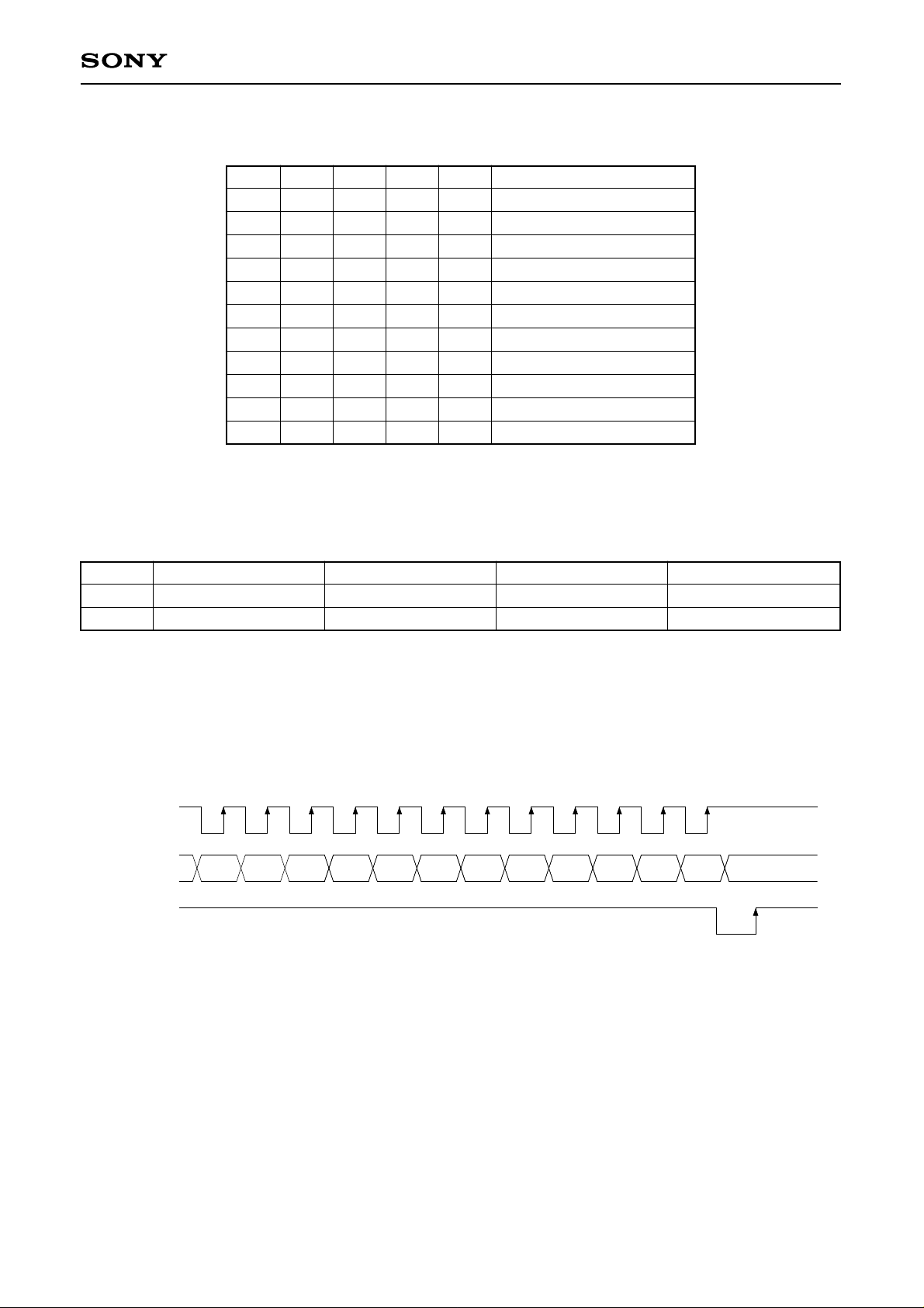
2-1-1. [Parallel input] (PS = H) — For high speed shutter only
Table of Shutter Settings
D1
ENB
X
L
H
L
H
X
X
X
X
X
X
ED0
L
H
H
H
H
H
H
H
H
H
H
ED1
X
H
H
L
L
H
L
H
L
H
L
ED2
X
H
H
H
H
L
L
H
H
L
L
X
H
H
H
H
H
H
L
L
L
L
Shutter speed
Shutter OFF
1/60 (s)
1/50 (s)
1/100 (s)
1/120 (s)
1/250 (s)
1/500 (s)
1/1000 (s)
1/2000 (s)
1/4000 (s)
1/10000 (s)
2-1-2. [Serial input] (PS = L)
The combination of serial data SMD1 and SMD2 can be used to select one of four modes.
Shutter Mode
Mode
SMD1
SMD2
Flickerless
Low
Low
High-speed shutter
Low
High
Low-speed shutter
High
Low
CXD1254AR/AQ
No shutter
High
High
• Flickerless Mode for eliminating flicker caused by oscillation frequency of fluorescent lights.
• High-speed shutter Shutter speed faster than 1/60 sec. (NTSC/EIA) or 1/50 sec. (CCIR).
• Low-speed shutter Shutter speed slower than 1/60 sec. (NTSC/EIA) or 1/50 sec. (CCIR).
• No shutter Shutter operation inactive.
ED1 (CLK)
ED2 (OATA)
EDO (STB)
D0 D1 D2 D3 D4 D5 D6 D7 D8 SMD1 SMD2
Dummy
ED2 data is latched in the register on the rising edge of ED1 and the register contents are transferred during
the low period of ED0.
—9—
Page 10
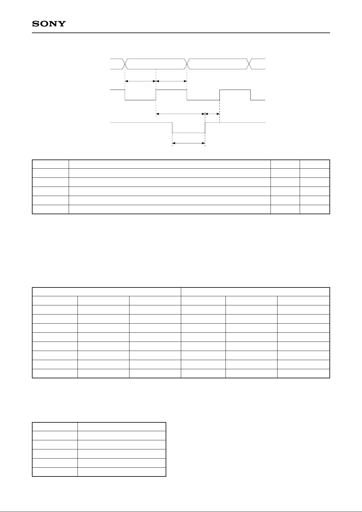
AC Characteristics
CXD1254AR/AQ
ED2
ts2 th2
ED1
ts1 ts0
ED0
tW0
Symbol
ts2
th2
ts2
tw0
ts0
ED2 set-up time referenced from the ED1 rising edge
ED2 hold-time referenced from the ED1 rising edge
ED1 rise set-up time referenced from the ED0 rising edge
ED0 pulse width
ED0 rise set-up time referenced from the ED1 rising edge
2-1-3. [Shutter speed calculation formula]
High-speed Shutter
• For NTSC/EIA
T= [26210 – (1FF16 – L16)] × 63.56 + 34.78 µs • L16: Load value
• For CCIR
T= [31210 – (1FF16 – L16)] × 64 + 35.6 µs
NTSC/EIA
Load value Shutter speed Calculated value
0FA16 1/10000 1/10169
0FC16 1/4000 1/4435
10016 1/2000 1/2085
10816 1/1000 1/1012
11816 1/500 1/499
13716 1/250 1/252
17616 1/125 1/125
19616 1/100 1/100
Load value Shutter speed Calculated value
0C816 1/10000 1/10040
0CA16 1/4000 1/4349
0CE16 1/2000 1/2068
0D616 1/1000 1/1004
0E616 1/500 1/495
10516 1/250 1/250
14316 1/125 1/125
14916 1/100 1/120
CCIR
Min.
20 ns
20 ns
20 ns
20 ns
20 ns
Max.
—
—
—
50 µs
—
Low-speed Shutter
N = 2 × (1FF16 – L16) FLD
“1FF” cannot be used as a load value.
Load value
1FE16
1FD16
:
10116
10016
Shutter speed (FLD)
2
4
:
508
510
—10—
Page 11
CXD1254AR/AQ
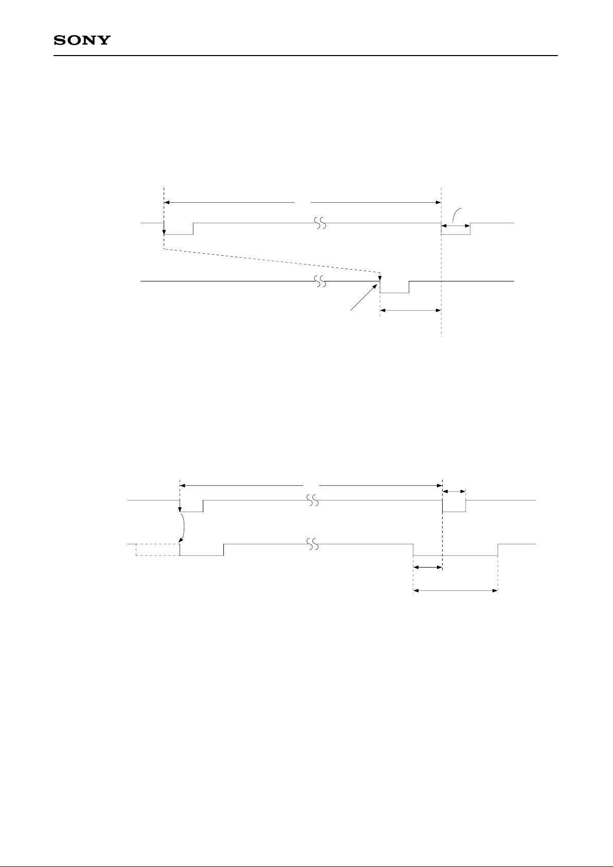
External Synchronization Mode Description
• H Reset
The reset process is started from the first falling edge of the inputted reset pulse. The next reset occurs
only when there is a divergence of at least a clock cycles (0.98 µs) from the edge.
The minimum reset pulse width is 0.98 µs.
The HD output reset position leads the H reset input by 2.45 to 2.94 µs.
1H
H reset input
HD output
HD pulse reset at the falling edge of 0.98µs and over
0.98µs and over
2.45 to 2.94µs
• V Reset
The VD output reset position leads the falling edge of the V reset input by 3.5 to 4.0 H for NTSC/EIA and by
3.0 to 3.5 H for PAL.
The minimum reset pulse width is 32 µs.
1V
V reset input
32µs and over
VD output
3.5 to 4.0H (NTSC/EIA)
3.0 to 3.5H (CCIR)
9H
—11—
Page 12

CXD1254AR/AQ
• For EIA (black & white), the TG system output follows the VD switching point by 1H. (for both ODD and EVEN.)
SYNC
BF
XSG1
VD
BLK
HD
FLD
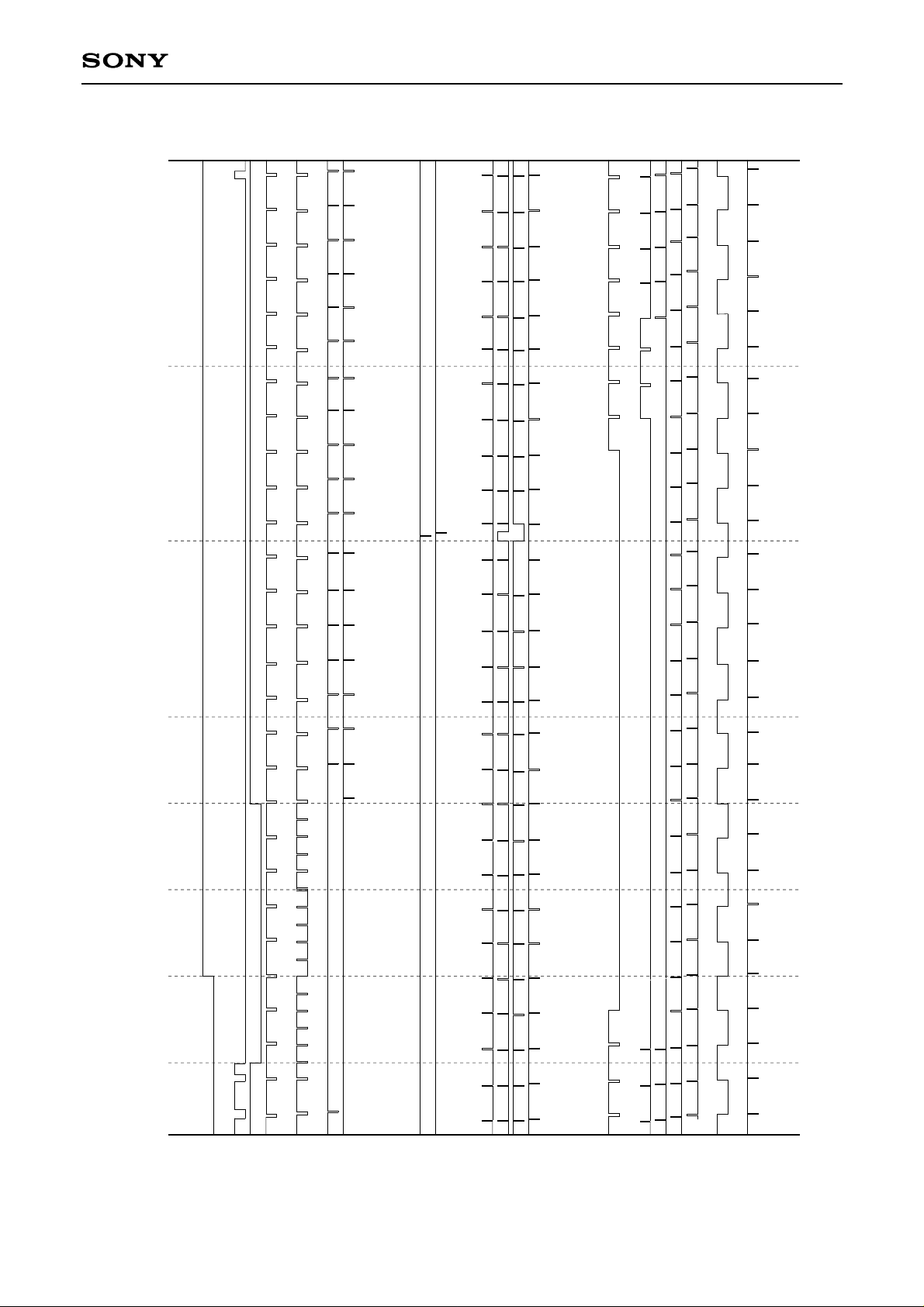
Timing Chart (1) <NTSC/EIA vertical direction>
ODD Field
XSG2
—12—
XV1
XV2
XV3
XV4
PBLK
CLP1
CLP2
CLP4
CLP3
ID
BFG
Page 13
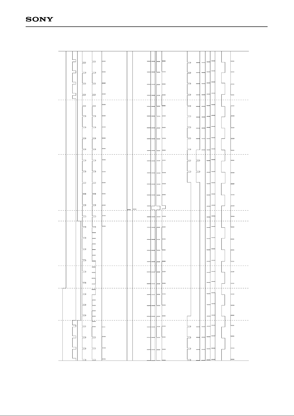
CXD1254AR/AQ
EVEN Field
FLD
BLK
VD
HD
SYNC
BF
XSG1
XSG2
XV1
—13—
XV2
XV3
XV4
PBLK
CLP1
CLP2
CLP3
CLP4
ID
BFG
Page 14
CXD1254AR/AQ
VD
FLD
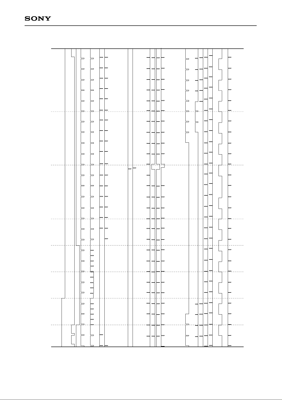
Timing Chart (2) <CCIR vertical direction>
ODD Field
HD
BLK
SYNC
BF (4–1)
BF (2–3)
XSG1
XSG2
—14—
XV1
XV2
XV3
XV4
ID
CLP1
CLP2
CLP3
PBLK
CLP4
BFG
Page 15
CXD1254AR/AQ
EVEN Field
VD
FLD
HD
BLK
SYNC
BF (3–4)
BF (1–2)
XSG1
XV1
XV2
XV3
XSG2
XV4
CLP1
CLP2
PBLK
CLP3
ID
CLP4
BFG
—15—
Page 16

CXD1254AR/AQ
Color
B/W
CL
HD
BLK
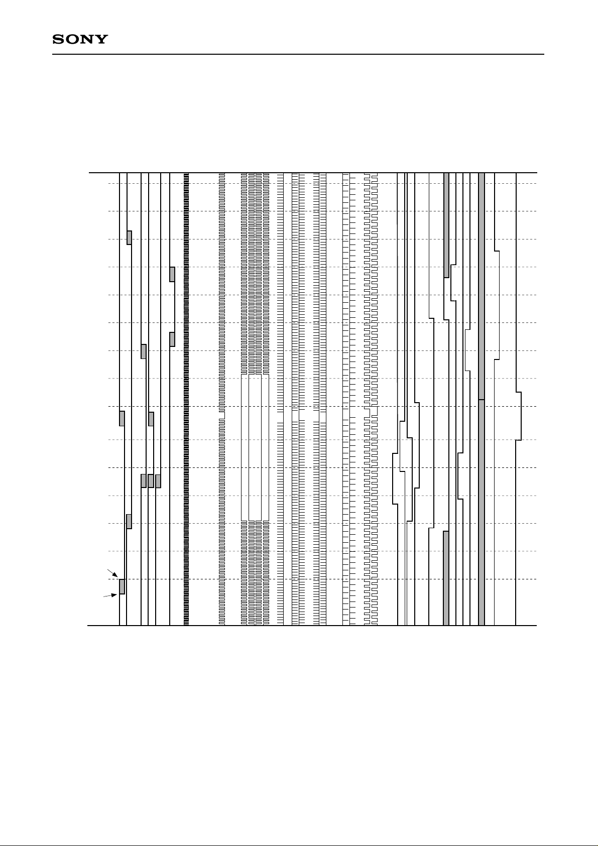
NTSC/EIA Normal Mode H Direction Timing Chart
Timing Chart (3) <NTSC/EIA horizontal direction, normal mode>
BF
EQ
HSYNC
VSYNC
CLK
H1H2H3
H4
RG
SHP
SHD
XSHP
XSHD
—16—
XSP1
XSP2
XV1
XV2
XV3
XDL1
XDL2
XV4
CLP1
PBLK
ID
CLP2
CLP3
CLP4
BFC
XSUB
Page 17
CXD1254AR/AQ
Color
B/W
CL
HD
BLK
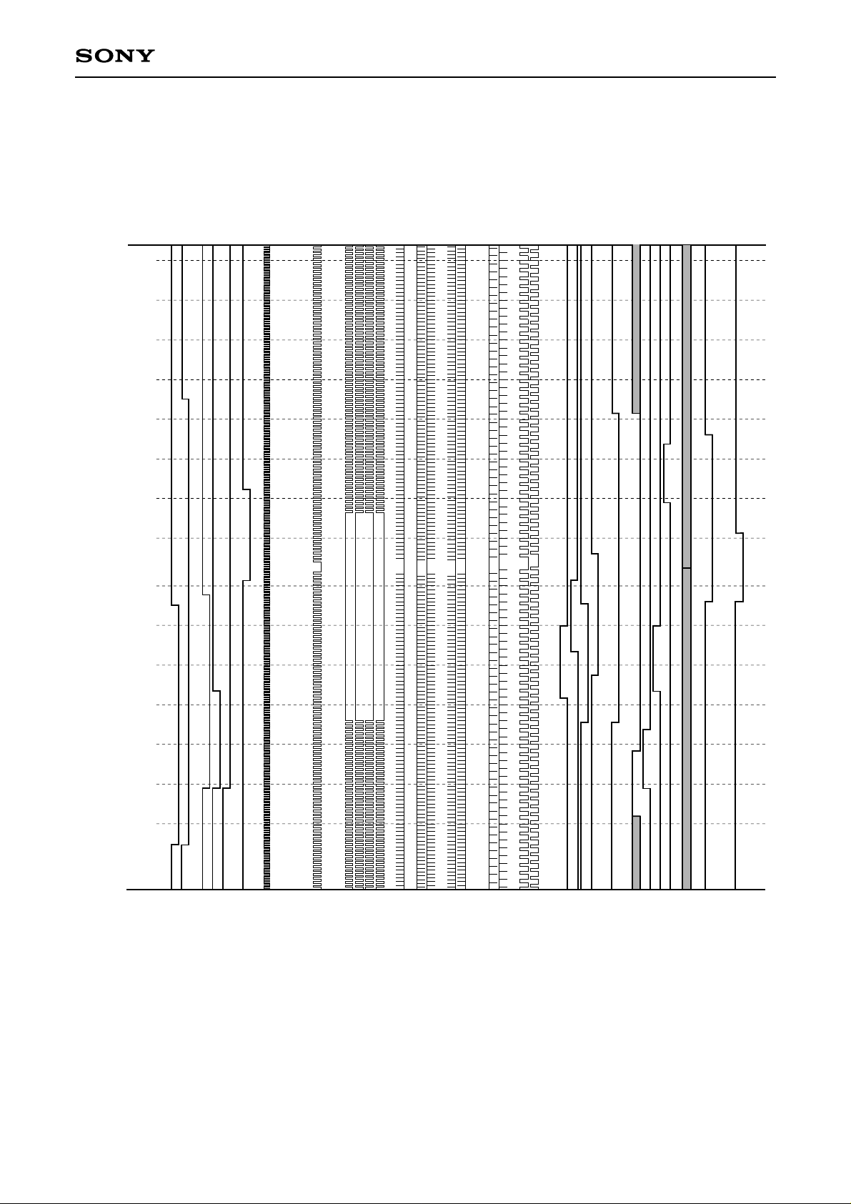
NTSC/EIA Mirror Mode H Direction Timing Chart
Timing Chart (4) <NTSC/EIA horizontal direction, mirror mode>
BF
EQ
HSYNC
VSYNC
CLK
H1H2H3
H4
RG
SHP
SHD
XSHP
XSHD
—17—
XSP1
XSP2
XV1
XV2
XV3
XDL1
XDL2
XV4
CLP1
PBLK
ID
CLP2
CLP3
CLP4
BFC
XSUB
Page 18
CXD1254AR/AQ
HD
EQ
BLK
HSYNC
CCIR Normal Mode H Direction Timing Chart
Timing Chart (5) <CCIR horizontal direction, normal mode>
CL
BF
VSYNC
CLK
H1H2H3
H4
RG
XSHP
XSHD
—18—
XV1
XV2
XV3
SHP
SHD
XSP1
XSP2
XDL1
XDL2
XV4
CLP1
CLP2
PBLK
ID
CLP3
BFC
CLP4
XSUB
Page 19
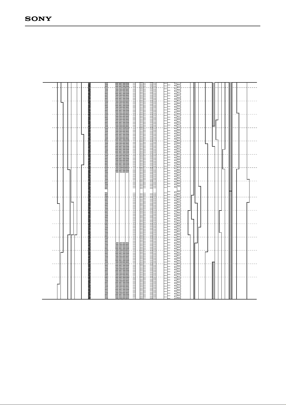
CXD1254AR/AQ
HD
EQ
BLK
HSYNC
CCIR Mirror Mode H Direction Timing Chart
Timing Chart (6) <CCIR horizontal direction, mirror mode>
CL
BF
VSYNC
CLK
H1H2H3
H4
RG
XSHP
XSHD
—19—
XV1
XV2
XV3
SHP
SHD
XSP1
XSP2
XDL1
XDL2
XV4
CLP1
CLP2
PBLK
ID
CLP3
CLP4
BFC
XSUB
Page 20
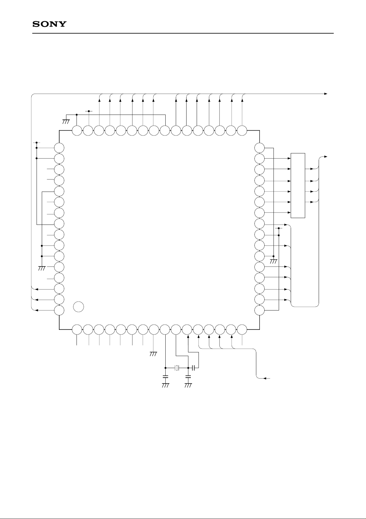
Application Circuit
(LQFP Package)
CXD1254AR/AQ
Signal Processing
33343536373839404142434445464748
49
50
51
52
53
54
55
56
57
58
59
60
61
62
63
64 17
CXD1254AR
32
31
30
29
28
27
26
25
24
23
22
21
20
19
18
CCD imase sensor
Driver
1 2 3 4 5 6 7 8 9 10 11 12 13 14 15 16
Shutter control
OSC NTSC/EIA : 28.6363MHz
CCIR : 28.375MHz
• Please use a clock crystal which
operates on a fundamental wave.
Application circuits shown are typical examples illustrating the operation of the devices. Sony cannot assume responsibility for
any problems arising out of the use of these circuits or for any infringement of third party patent and other right due to same.
—20—
Page 21
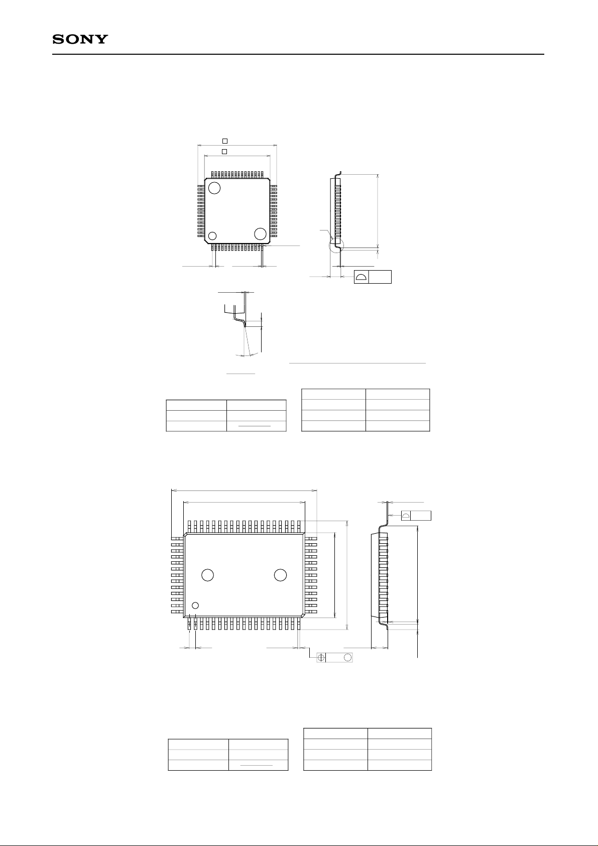
Package Outline Unit : mm
CXD1254AR/AQ
CXD1254AR
49
64
0.5 ± 0.08
SONY CODE
EIAJ CODE
JEDEC CODE
∗ 10.0 ± 0.1
48
1
0.1 ± 0.1
0° to 10°
64PIN LQFP (PLASTIC)
12.0 ± 0.2
33
16
+ 0.08
0.18 – 0.03
0.5 ± 0.2
DETAIL A
LQFP-64P-L01
QFP064-P-1010
32
(11.0)
A
17
(0.22)
+ 0.2
1.5 – 0.1
0.127 – 0.02
0.5 ± 0.2
+ 0.05
0.1
NOTE: “∗” Dimensions do not include mold protrusion.
PACKAGE STRUCTURE
PACKAGE MATERIAL
LEAD TREATMENT
LEAD MATERIAL
PACKAGE WEIGHT
EPOXY / PHENOL RESIN
SOLDER/PALLADIUM
42/COPPER ALLOY
0.3g
PLATING
CXD1254AQ
52
64
SONY CODE
EIAJ CODE
JEDEC CODE
64PIN QFP(PLASTIC)
23.9 ± 0.4
+ 0.4
20.0 – 0.1
51
1
1.0
+ 0.15
0.4 – 0.1
33
32
+ 0.4
14.0 – 0.1
17.9 ± 0.4
20
19
± 0.12
+ 0.35
2.75 – 0.15
M
PACKAGE STRUCTURE
QFP–64P–L01
∗
QFP064–P–1420
PACKAGE MATERIAL
LEAD TREATMENT
LEAD MATERIAL
PACKAGE WEIGHT
EPOXY RESIN
SOLDER/PALLADIUM
COPPER /42 ALLOY
1.5g
+ 0.1
0.15 – 0.05
+ 0.2
0.1 – 0.05
PLATING
0.15
16.3
0.8 ± 0.2
—21—
 Loading...