

Page 1

CXD1250M/N
Vertical Clock Driver for CCD Image sensor
Description
CXD1250M/N is a clock driver developed for the
vertical register drive of CCD Image sensor.
Features
4-channel vertical clock driver and 1 channel
substrate driver are built-in.
Application
CCD camera
Structure
CMOS
Absolute Maximum Ratings (Ta = 25°C)
• Supply voltage VDD VL – 0.3 to VL + 35.0 V
VM VL – 0.3 to VL + 35.0 V
VH VL – 0.3 to VL + 35.0 V
VHH VL – 0.3 to VL + 35.0 V
• Input volltage VI VL – 0.3 to VDD + 0.3 V
• Output voltage MVφ (pins 13, 17) VL – 0.3 to VM + 0.3 V
• Output voltage HVφ (pins 14, 16) VL – 0.3 to VH + 0.3 V
• Output voltage HHVφ (pin 19) VL – 0.3 to VHH + 0.3 V
• Operating temperature Topr –25 to +85 °C
• Storage temperature Tstg –40 to +125 °C
CXD1250M
20 pin SOP (Plastic)
CXD1250N
20 pin SSOP (Plastic)
Recommended Operating Conditions
• Supply voltage VDD 5.0 ± 0.5 V
VM VL + 10.0 V
VH VL + 25.0 V
VHH VL + 30.0 V
VL –10.0 V
• Operating temperature Topr –20 to +75 °C
Sony reserves the right to change products and specifications without prior notice. This information does not convey any license by
any implication or otherwise under any patents or other right. Application circuits shown, if any, are typical examples illustrating the
operation of the devices. Sony cannot assume responsibility for any problems arising out of the use of these circuits.
– 1 –
80639C43-PK
Page 2
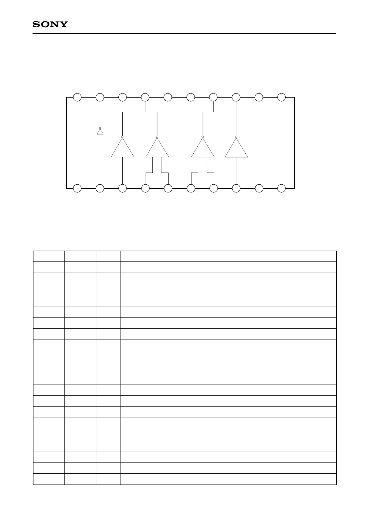
Block Diagram and Pin Configuration (Top View)
CXD1250M/N
Pin Description
No.
Symbol I/O Description
20
1
(20V)
HH
V
GND
19
Vsub
2
Xsub
(–10V)
L
V
18
3
XV2
17
4
Vφ2
XV1
16
5
Vφ1
XSG1
6
(0V)
M
V
XV3
1415
7
Vφ3
XSG2
13
8
Vφ4
XV4
12
9
(15V)
H
V
(5V)
DD
V
N.C
11
10
N.C
1
2
3
4
5
6
7
8
9
10
11
12
13
14
15
16
17
GND
Xsub
XV2
XV1
XSG1
XV3
XSG2
XV4
VDD
NC
NC
VH
Vφ4
Vφ3
VM
Vφ1
Vφ2
—
—
—
—
—
O
O
—
O
O
GND
I
Output control (Vsub)
I
Output control (Vφ2)
I
Output control (Vφ1)
I
Output control (Vφ1)
I
Output control (Vφ3)
I
Output control (Vφ3)
I
Output control (Vφ4)
Power supply (5V)
Power supply (15V)
Output (2 level : VM, VL)
Output (3 level : VH, VM, VL)
Power supply (0V)
Output (3 level : VH, VM, VL)
Output (2 level : VM, VL)
18
19
20
VL
Vsub
VHH
—
O
—
Power supply (–10V)
Output (2 level : VHH, VL)
Power supply (20V)
– 2 –
Page 3
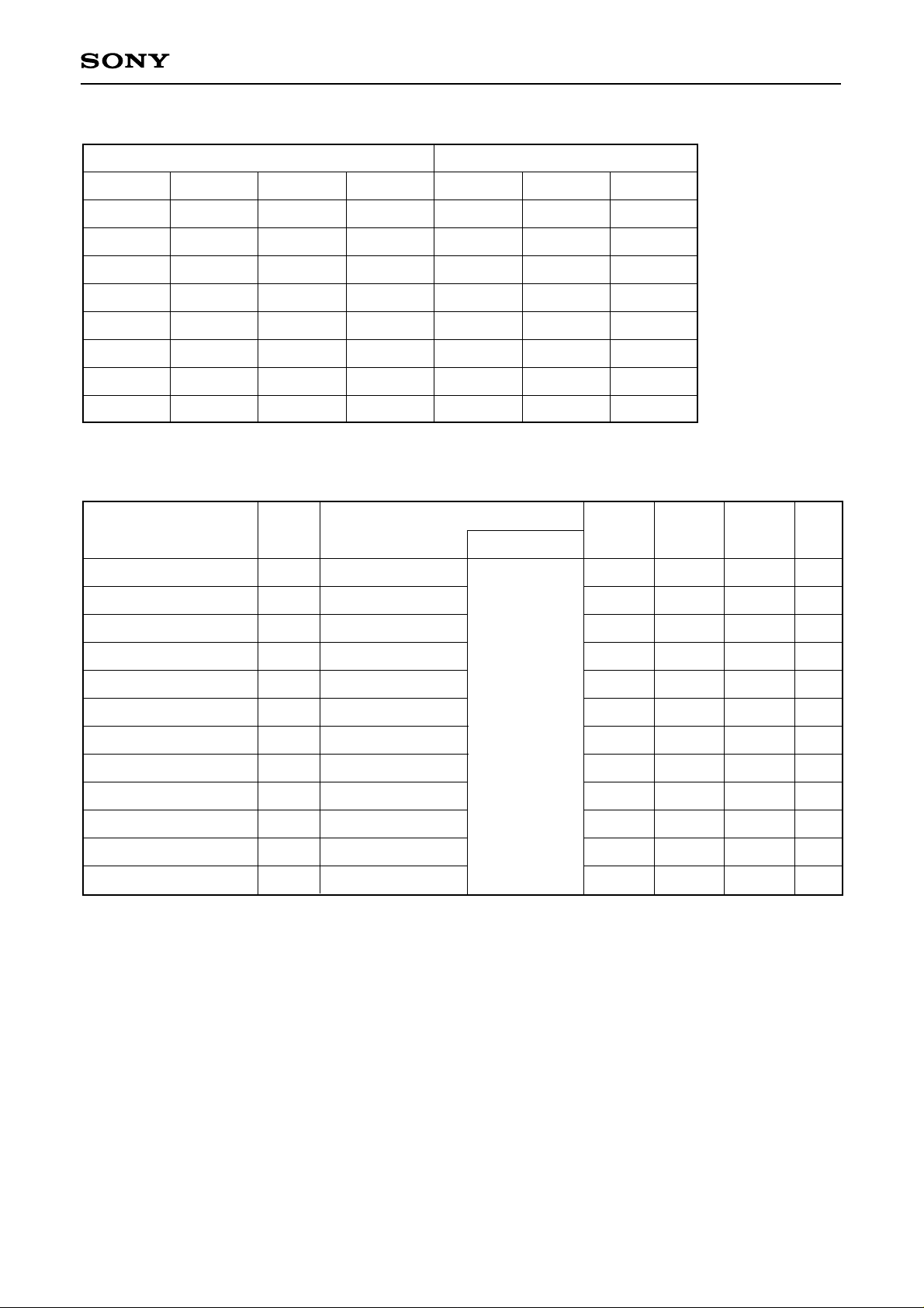
Truth Table
CXD1250M/N
Input
XV1 · 3
L
H
X
X
X
X
L
H
XSG1 · 2 XV2 · 4 Xsub
H
H
X
X
X
X
L
L
DC Characteristics (Ta = 25°C)
Item
"H" level input voltage
"L" level input voltage
Symbol Min. Typ. Max. Unit
VIH
VIL
Output
Vφ1 · 3 Vφ2 · 4
X
X
L
H
X
X
X
X
X
X
X
X
L
H
X
X
VM
VL
X
X
X
X
VH
Z
X
X
VM
VL
X
X
X
X
Vsub
X
X
X
X
VHH
VL
X
X
X : Don't care
Z : High impedance
Test condition
Power supply
3.5
—
—
—
—
1.5
V
V
"L" level output voltage
"M" level output voltage
"M" level output voltage
"H" level output voltage
"HH" level output voltage
Input current
Power supply current
Power supply current
Power supply current
Power supply current
∗
Suuply current at operation (See the Test Circuit)
VφL
VφM
VφM
VφH
VφHH
IφL = 20µA
IφM = –20µA
IφM = 20µA
IφH = –20µA
IφHH = –20µA
Ii
∗
IM
∗
IDD
∗
IH
∗
IHH
VDD = 5V
VL = –10V
VM = 0V
VH = 15V
VHH = 20V
—
—
–0.1
14.9
19.9
—
—
—
—
—
–10
0.0
0.0
15
20
1.0
4.5
0.3
0.1
0.05
–9.9
0.1
—
—
—
—
5.0
0.5
0.2
0.1
V
V
V
V
V
µA
mA
mA
mA
mA
– 3 –
Page 4
CXD1250M/N
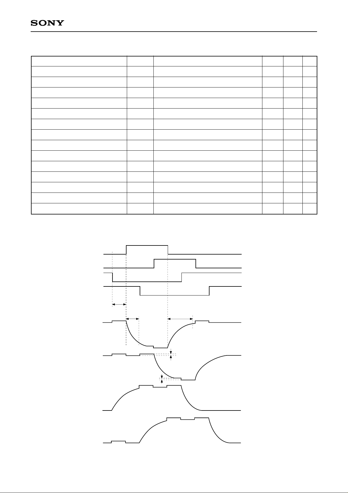
Switching Characteristics
(See the Test Circuit Ta = 25°C, VHH = 20V, VH = 15V, VM = 0V, VL = –10V, VDD = 5V)
Item
Output current
Output current
Output current
Output current
Output current
Output current
Rise time VL → VM
Fall time VM → VL
Rise time VM → VH
Fall time VH → VM
Rise time VL → VHH
Fall time VHH → VL
Coupling amplitude (middle level)
Coupling amplitude (low level)
Symbol Conditions Max. Min. Unit
IL
IM1
IM2
IH
ISL
ISH
TTLM
TTML
TTMH
TTHM
TTLHH
TTHHL
VCOM
VCOL
Vφ1 to 4 = –9.5V
Vφ1 to 4 = –0.5V
Vφ1, 3 = 0.5V
Vφ1, 3 = 14.5V
Vsub = –9.5V
Vsub = –19.5V
Vφ1 to 4 = –0.5V After input transient
Vφ1 to 4 = –9.5V After input transient
Vφ1, 3 = 14V After input transient
Vφ1, 3 = 1V After input transient
Vsub = 17V After input transient
Vsub = –7V After input transient
Vφ1 to 4
Vφ1 to 4
–25
–9
–12
1000
500
1000
1000
200
200
0.5
0.5
10
12
7
mA
mA
mA
mA
mA
mA
ns
ns
ns
ns
ns
ns
V
V
Input Waveform (Repeat Cycle 15.7kHz)
5
XV1
0
5
XV2
0
5
XV3
0
5
XV4
0
600ns
T
TML
Output Waveform
0
Vφ1
–10
0
Vφ2
–10
0
Vφ3
TTLM
VCOM
VCOL
Vφ4
–10
0
–10
– 4 –
Page 5

Switching Waveform
Input Waveform
5
XV1
0
5
XV3
0
5
XSG1
0
5
XSG2
0
TMH TTHM
T
Output Waveform
15
0
Vφ1
–10
CXD1250M/N
16.6ms
15
Vφ3
0
–10
0
Vφ2
–10
Test Circuit
500pF
20V –10V
19
20
18
17
R1
C1
16
R1
C2
0V
C2
5
Xsub
0
TTLHH TTHHL
20
Vsub
–10
1
C
C2
C2
C1
R2
1415
13
C1
12
R1
R1
11
R1; 27Ω
R2; 5Ω
C1; 1500pF
C2; 3300pF
15V
6
1
2
3
Timing generator
5
4
(CXD1156Q)
7
9
8
10
5V
– 5 –
Page 6
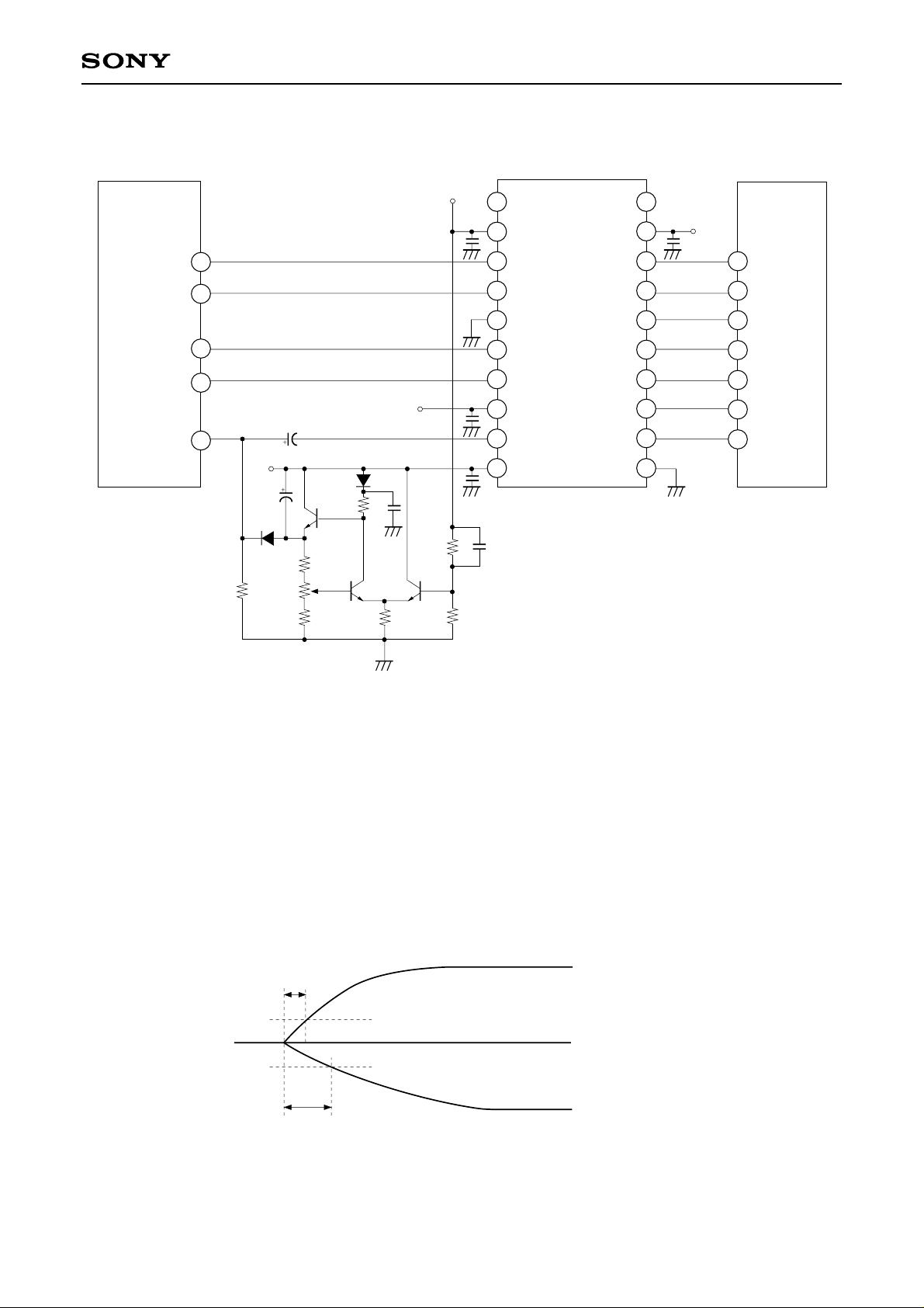
Application Circuit
ICX026/027 CXD1250M/N CXD1156Q
Vφ4
+15V
1
11
12
13
NC
V
Vφ4
10
NC
H
VDD
XV4
9
8
+5V
CXD1250M/N
4
XV4
Vφ3
27k
14
15
16
17
18
19
20
0.1µ
VM
Vφ1
Vφ2
VL
Vsub
VHH
Refer to the Caution : Rise in power supply
Vφ3
2
Vφ1
6
Vφ2
3
1µ/35
sub
4
+20V
4.7µ/
37
15k
1M
Note:
The capacitor more than 0.1µF should be connected between the ground and each pin of V
47k
15k
270k
–10V
0.1µ
56k
39k
7
XSG2
6
XV3
5
XSG1
XV1
4
XV2
3
Vsub
2
GND
1
DD, VH, VHH and VL .
10
11
21
VSG2
XV3
8
VSG1
XV1
9
XV2
5
Xsub
Caution : Rise in Power Supply
When the substrate driver is in use, be careful not to let the CCD imagesensors Sub (pin 4) turn into
negative voltage.
To this end, raise VL and VHH at the application circuit under the following conditions.
HH (20V)
V
t1
20%
0V
20%
t2
t
2 ≥ t1 ≥ 10msec
VL (–10V)
– 6 –
Page 7
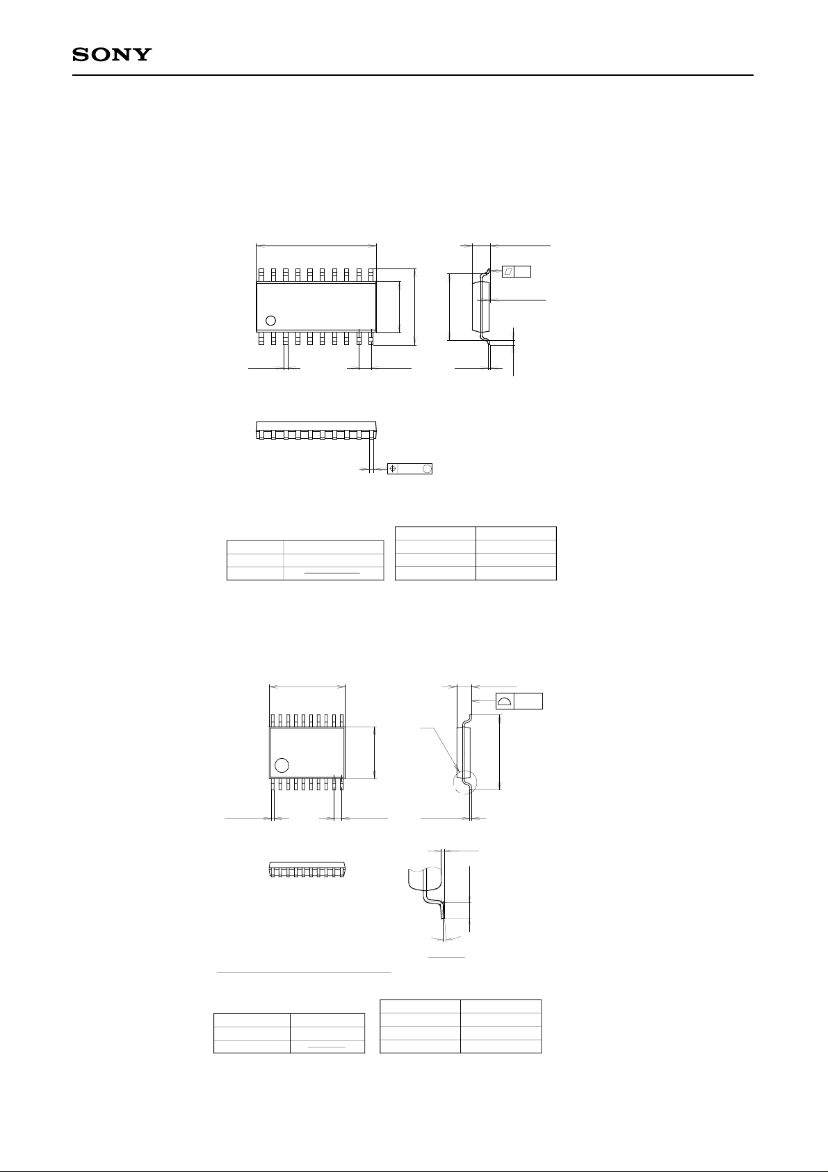
Package Outline Unit: mm
CXD1250M
CXD1250M/N
20PIN SOP (PLASTIC) 300mil
CXD1250N
20
1
0.45 ± 0.1
SONY CODE
EIAJ CODE
JEDEC CODE
+ 0.4
12.45 – 0.1
SOP-20P-L01
∗SOP020-P-0300-A
11
+ 0.3
5.3 – 0.1
7.9 ± 0.4
10
1.27
± 0.12
PACKAGE STRUCTURE
PACKAGE MATERIAL
LEAD TREATMENT
LEAD MATERIAL
PACKAGE WEIGHT
+ 0.4
1.85 – 0.15
0.15
+ 0.2
6.9
+ 0.1
0.2 – 0.05
M
0.1 – 0.05
0.5 ± 0.2
EPOXY / PHENOL RESIN
SOLDER PLATING
COPPER ALLOY
0.3g
20PIN SSOP (PLASTIC)
∗6.5 ± 0.1
20
1
+ 0.1
0.22 – 0.05
NOTE: Dimension “∗” does not include mold protrusion.
SONY CODE
EIAJ CODE
JEDEC CODE
11
SSOP-20P-L01
SSOP020-P-0044
∗4.4 ± 0.1
10
0.65 ± 0.12
A
+ 0.05
0.15 – 0.02
0.1 ± 0.1
0.5 ± 0.2
0° to 10°
DETAIL A
PACKAGE STRUCTURE
PACKAGE MATERIAL
LEAD TREATMENT
LEAD MATERIAL
PACKAGE WEIGHT
EPOXY RESIN
SOLDER / PALLADIUM
COPPER / 42 ALLOY
0.1g
+ 0.2
1.25 – 0.1
6.4 ± 0.2
0.1
PLATING
– 7 –
 Loading...