

Page 1

—1—
E93512A78-TE
Sony reserves the right to change products and specifications without prior notice. This information does not convey any license by
any implication or otherwise under any patents or other right. Application circuits shown, if any, are typical examples illustrating the
operation of the devices. Sony cannot assume responsibility for any problems arising out of the use of these circuits.
Absolute Maximum Ratings (Ta=25 °C)
• Supply voltage VDD –0.5 to +7.0 V
• Input voltage VI –0.5 to VDD +0.5 V
• Output voltage VO –0.5 to VDD +0.5 V
• Operating temperature Topr –20 to +75 °C
• Storage temperature Tstg –55 to +150 °C
Recommended Operating Conditions
• Supply voltage VDD +4.5 to +5.5 V
(standard +5.0)
• Operating temperature Topr –20 to +75 °C
Description
The CXD1186C is a CD-ROM decoder LSI.
Features
• Corresponds to CD-ROM, CD-I and CD-ROM XA
formats.
• Real time error correction. (Erasure correction
using C2 pointer from CD player.)
• Double speed playback.
• Connection to standard SRAM up to 64 K bytes, as
buffer memory, possible.
Applications
CD-ROM driver
Structure
Silicon gate CMOS IC
CD-ROM Decoder
CXD1186CQ CXD1186CR
80 pin QFP (Plastic) 80 pin LQFP (Plastic)
CXD1186CQ/CR
For the availability of this product, please contact the sales office.
Page 2
—2—
CXD1186CQ/CR
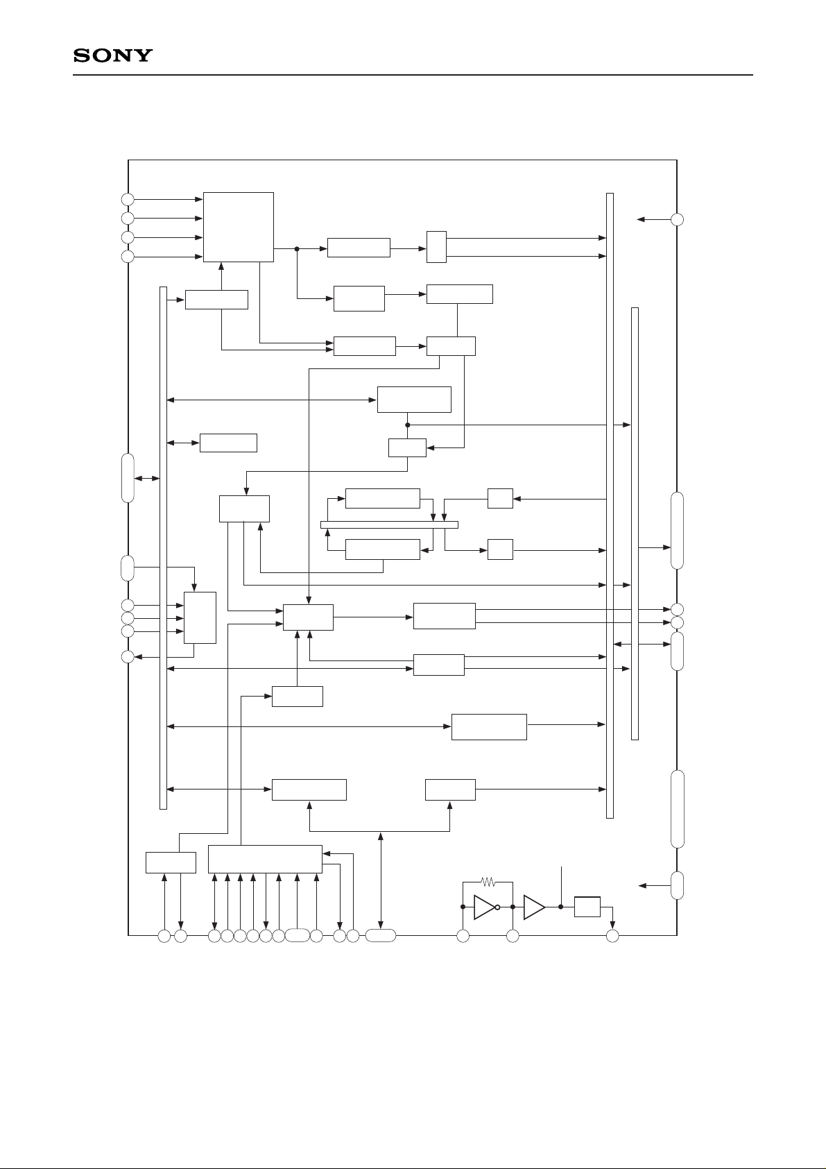
Block Diagram
DATA
BCLK
C2PO
LRCK
CDP I/F
CONTROL REG
DESCRAMBLE
SYNC
CONTROL
+2
HCLK
XTL2
XTL1
HDB0-7, P
HMDS
ADRQ
XAAC
HA0, 1
XTC
HINT
S/P
WORD CENTER
DECODETIMING GEN
DRIIVE ADDRESS
COUNTER
LATCH
REGISTERS
ECC
CONTROL
GALOIS FIELD
REG
REGSYNDROME
CPU
I/F
PRIORITY
RESOLVER
DMA
SEQUENCER
CPU DMA
DB0–7
A0–3
INT
HOST DMA
HOST ADDRESS
COUNTER
HOST I/F REGS DMA FIFO
ADP I/F
HOST I/F REGS
VDD
GND
BDB0–7, P
BA0–15
XRST
XWR
XRD
XCS
HDBP
XHWR
XHRD
XHCS
XDRQ
XHAC
XMWR
XMOE
Page 3

—3—
CXD1186CQ/CR
Pin Configuration
CXD1186CQ
1 2 3 4 5 6 7 8 9 10 11 14 1512 13 16 17 20 2118 19 23 24
25
26
27
28
29
30
31
32
33
34
35
36
37
38
39
40
22
64 63 62 61 60 59 58 57 56 55 54 51 5053 52 49 48 45 4447 46 42 4143
INT
GNDA0A1A2A3
HMDS
HA0
HA1
XHCS
HINT
GND
XHRD
XHWR
HDB0
HDB1
HDB2
HDB3
HDB4
HDB5
HDB6
HDB7
GND
HDBP
BA8
BA7
BA6
BA5
BA4
BA3
BA2
VDD
BA1
BA0
XAAC
ADRQ
XTC
XHAC
HDRQ
79
80
78
77
76
75
74
73
72
71
70
69
68
67
66
65
XRST
HCLK
GND
XTL1
XTL2
BDBP
BDB7
BDB6
BDB5
BDB4
BDB3
BDB2
BDB1
GND
BDB0
XMWR
XMOE
BA15
BA14
BA13
BA12
BA11
BA10
GND
BA9
LRCK
DATA
BCLK
C2PO
DB0
DB1
DB2
DB3
VDD
DB4
DB5
DB6
DB7
XCS
XRD
XWR
CXD1186CR
1 2 3 4 5 6 7 8 9 10 11 14 1512 13 16 172018 19
25
26
27
28
21
22
23
24
29
30
31
32
33
34
35
36
37
38
39
40
60 59 58 57 56 55 54 51 5053 52 49 48 45 4447 46 42 4143
A0A1A2A3HMDS
HA0
HA1
XHCS
HINT
GND
XHRD
XHWR
HDB0
HDB1
HDB2
HDB3
HDB4
HDB5
HDB6
HDB7
GND
BA9
BA8
BA7
BA6
BA5
BA4
BA3
BA1
V
DD
BA1
FA0
XAAC
ADRQ
XTC
79
80
78
77
76
75
74
73
72
71
70
69
68
67
66
65
XHAC
HDRQ
XRST
HDRP
GND
XTL1
XTL2
BDBP
BDB7
BDB6
BDB5
BDB4
BDB3
BDB2
BDB1
GND
BDB0
XMWR
XMOE
BA15
BA14
BA13
BA12
BA11
BA10
BCLK
C2PO
DB0
DB1
64
63
62
61
GND
HCLK
LRCK
DATA
DB2
DB3
V
DD
DB4
DB5
DB6
DB7
XCS
XRD
XWR
INT
GND
Page 4
—4—
CXD1186CQ/CR
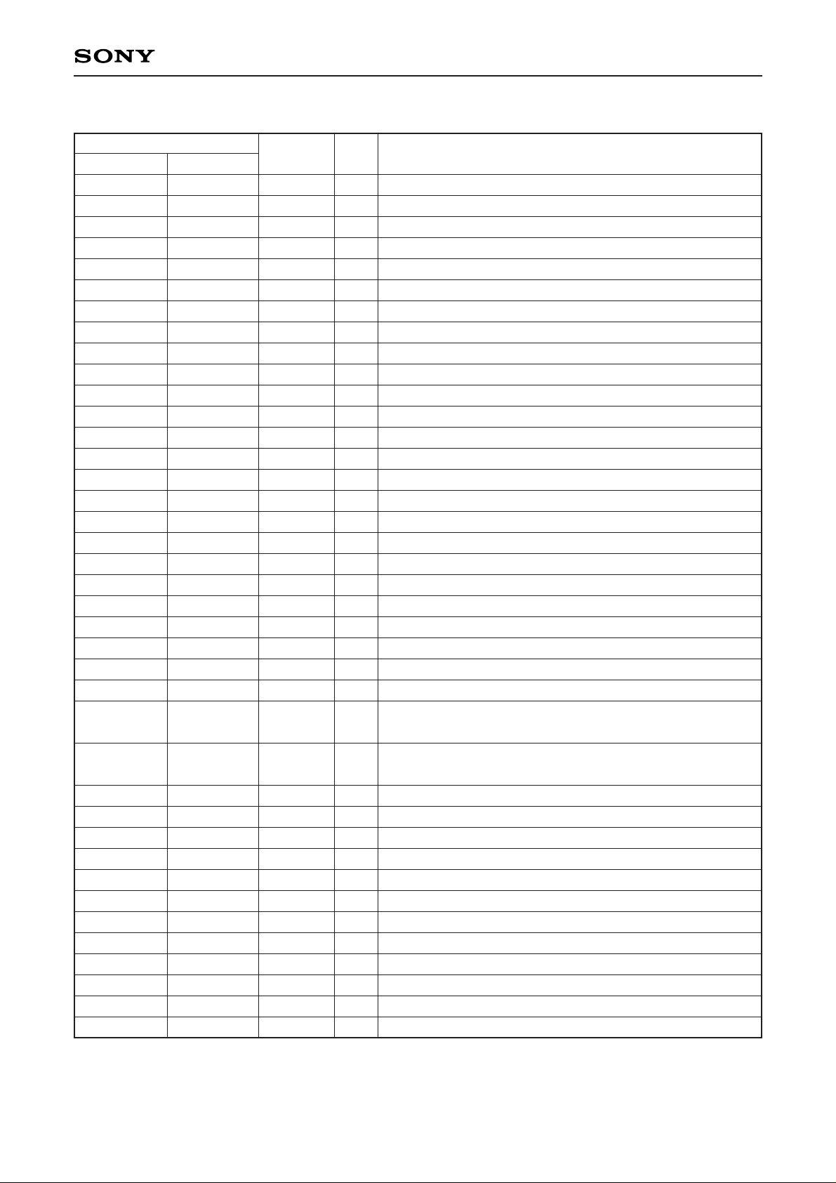
Pin Description
Pin No.
Symbol I/O Description
CXD1186CQ CXD1186CR
1
2
3
4
5
6
7
8
9
10
11
12
13
14
15
16
17
18
19
20
21
22
23
24
25
26
27
28
29
30
31
32
33
34
35
36
37
38
39
79
80
1
2
3
4
5
6
7
8
9
10
11
12
13
14
15
16
17
18
19
20
21
22
23
24
25
26
27
28
29
30
31
32
33
34
35
36
37
INT
GND
A0
A1
A2
A3
HMDS
HA0
HA1
XHCS
HINT
GND
XHRD
XHWR
HDB0
HDB1
HDB2
HDB3
HDB4
HDB5
HDB6
HDB7
GND
HDBP
XRST
HDRQ
XHAC
XTC
ADRQ
XAAC
BA0
BA1
VDD
BA2
BA3
BA4
BA5
BA8
BA7
O
—
I
I
I
I
I
I
I
I
O
—
I/O
I/O
I/O
I/O
I/O
I/O
I/O
I/O
I/O
I/O
—
I/O
I
O
I
I
I
O
O
O
—
O
O
O
O
O
O
Interrupt request signal to CPU
GND pin
CPU address signal
CPU address signal
CPU address signal
CPU address signal
Host mode select signal
Host address signal
Host address signal
Chip select negative logic signal from host
Interrupt request negative logic signal to host
GND pin
Data read strobe signal from host or to SCSI control IC
Data write strobe signal from host or to SCSI control IC
Host data bus
Host data bus
Host data bus
Host data bus
Host data bus
Host data bus
Host data bus
Host data bus
GND pin
Error flag, Host data bus
Reset negative logic signal
Data request positive logic signal to host. Or DMA
acknowledge negative logic signal to SCSI control IC
DMA acknowledge negative logic signal from host.
Or data request positive logic signal from SCSI control IC
Terminal count negative logic signal
DMA request positive logic signal from ADP
DMA acknowledge negative logic signal to ADP
Buffer memory address
Buffer memory address
Power (+5 V) supply pin
Buffer memory address
Buffer memory address
Buffer memory address
Buffer memory address
Buffer memory address
Buffer memory address
Page 5

—5—
CXD1186CQ/CR
Pin No.
Symbol I/O Description
CXD1186CQ CXD1186CR
40
41
42
43
44
45
46
47
48
49
50
51
52
53
54
55
56
57
58
59
60
61
62
63
64
65
66
67
68
69
70
71
72
73
74
75
76
77
78
79
80
38
39
40
41
42
43
44
45
46
47
48
49
50
51
52
53
54
55
56
57
58
59
60
61
62
63
64
65
66
67
68
69
70
71
72
73
74
75
76
77
78
BA8
BA9
GND
BA10
BA11
BA12
BA13
BA14
BA15
XMOE
XMWR
BDB0
GND
BDB1
BDB2
BDB3
BDB4
BDB5
BDB6
BDB7
BDBP
XTL2
XTL1
GND
HCLK
LRCK
DATA
BCLK
C2PO
DB0
DB1
DB2
DB3
VDD
DB4
DB5
DB6
DB7
XCS
XRD
XWR
O
O
—
O
O
O
O
O
O
O
O
I/O
—
I/O
I/O
I/O
I/O
I/O
I/O
I/O
I/O
O
I
—
O
I
I
I
I
I/O
I/O
I/O
I/O
—
I/O
I/O
I/O
I/O
I
I
I
Buffer memory address
Buffer memory address
GND pin
Buffer memory address
Buffer memory address
Buffer memory address
Buffer memory address
Buffer memory address
Buffer memory address
Buffer memory output enable negative logic signal
Buffer memory write negative logic signal
Buffer memory data bus
GND pin
Buffer memory data bus
Buffer memory data bus
Buffer memory data bus
Buffer memory data bus
Buffer memory data bus
Buffer memory data bus
Buffer memory data bus
Buffer memory pointer data bus
Crystal oscillation circuit output pin
Crystal oscillation circuit input pin
GND pin
1/2 frequency divided clock signal of XTL1
LR clock from CD player
Serial data from CD player
Bit clock from CD player
C2 pointer from CD player
CPU data bus
CPU data bus
CPU data bus
CPU data bus
Power (+5 V) supply pin
CPU data bus
CPU data bus
CPU data bus
CPU data bus
Chip select negative logic signal from CPU
CPU strobe negative logic signal to read out this IC internal
register
CPU strobe negative logic signal to write in this IC internal
register
Page 6

—6—
CXD1186CQ/CR
Electrical Characteristics
DC characteristics (VDD=5 V±10 %, VSS=0 V, Topr=–20 to +75 °C)
Item
Input voltage
H level
L level
TTL Schmitt hysterisis
Input current of pull up input
Input current of pull down input
Output voltage
H level
L level
Open drain output L level
Oscillation cell H level
input voltage L level
Logic threshold value
Feedback resistance
Output voltage
H level
L level
Symbol
VIH1
VIL1
(Vt+)–(Vt–)
IIL
IIH
VOH1
VOL1
VOL2
VIH
VIL
LVth
RFB
VOH
VOL
Conditions
VIL=0 V
VIH=VDD
IOH=–2 mA
IOL=4 mA
IOL=4 mA
VIN=VSS or VDD
IOH=–1 mA
IOL=1 mA
Min. Typ. Max. Unit
2.2 V
0.8 V
0.2 0.4 V
–40 –100 –240 µA
40 100 240 µA
VDD–0.8 V
0.4 V
0.4 V
0.7 VDD V
0.3 VDD V
VDD/2 V
250 k 1 M 2.5 M Ω
VDD/2 V
VDD/2 V
• Input pin with pull up resistance : XHCS, HA0, HA1, XTC
• Input pin with pull down resistance : C2PO, HMDS, ADRQ
• TTL Schmitt input pin : XRST
• Open drain output pin : HINT
• Two-way data bus always pulled up.
• Oscillation cell
Input : XTL1
Output : XTL2
I/O capacitance VDD=VI=0 V, f=1 MHz
Item
Input pin
Output pin
I/O pin
Symbol
CIN
COUT
CI/O
Min. Typ. Max.
9
11
11
Unit
pF
pF
pF
Page 7
—7—
CXD1186CQ/CR
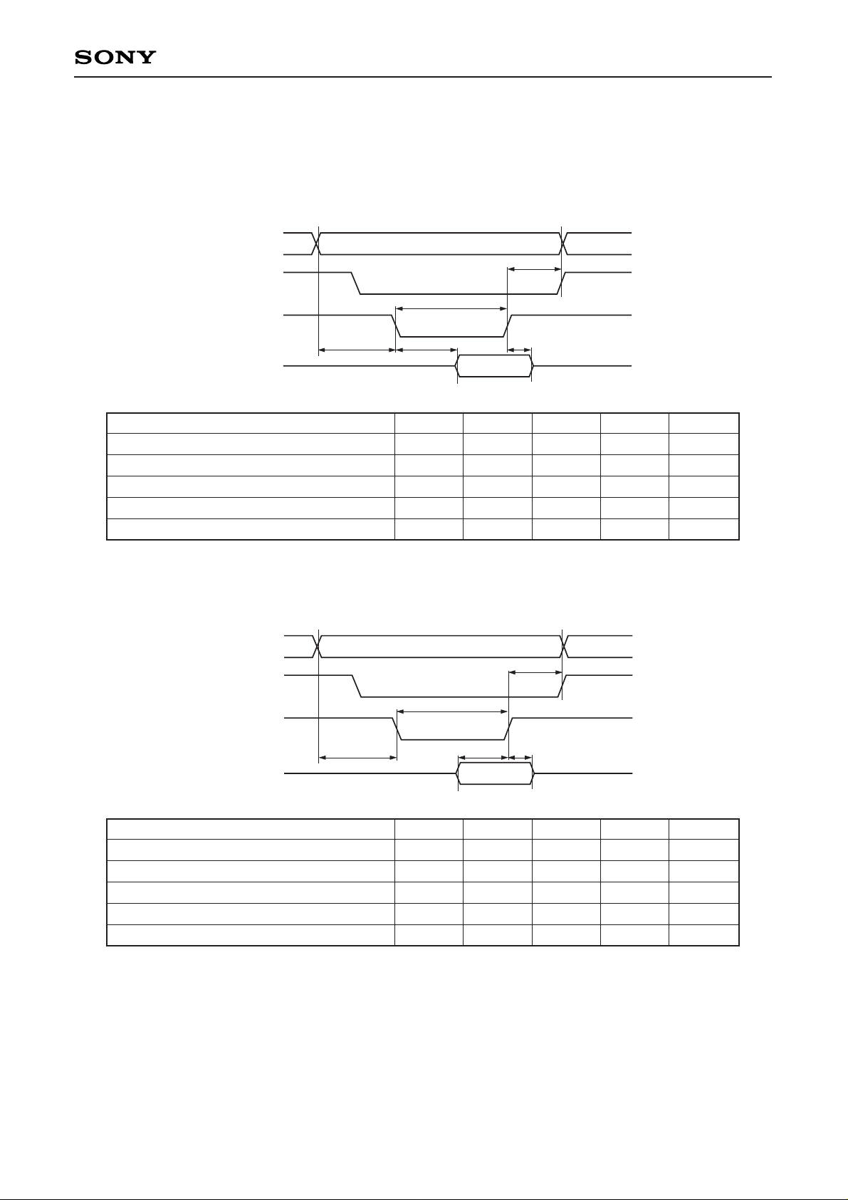
AC characteristics (Ta=–20 to +75 °C, VDD=5 V±10 %, Output Load=50 pF, f≤ 24.576 MHz)
1. CPU interface
(1) Read
(2) Write
A0 to 3
XCS
XRD
DB0 to 7
t
HRA
tRRL
tSAR tDRD
tFRD
Item
Address setup time (vs. XCS & XRD ↓)
Address hold time (vs. XCS & XRD ↑)
Data delay time (vs. XCS & XRD ↓)
Data float time (vs. XCS & XRD ↑)
Low level XRD pulse width
Symbol
tSAR
tHRA
tDRD
tFRD
tRRL
Min.
30
20
0
100
Typ. Max.
60
10
Unit
n
n
n
n
n
A0 to 3
XCS
XWR
DB0 to 7
t
HWD
tHWA
tSDW
tWWL
tSAW
Item
Address setup time (vs. XCS & XWR ↓)
Address hold time (vs. XCS & XWR ↑)
Data setup time (vs. XCS & XWR ↑)
Data hold time (vs. XCS & XWR ↑)
Low level XWR pulse width
Symbol
tSAW
tHWA
tSDW
tHWD
tWWL
Min.
30
20
40
10
50
Typ. Max. Unit
n
n
n
n
n
Where & in the chart indicates logical multiplication.
Page 8
—8—
CXD1186CQ/CR
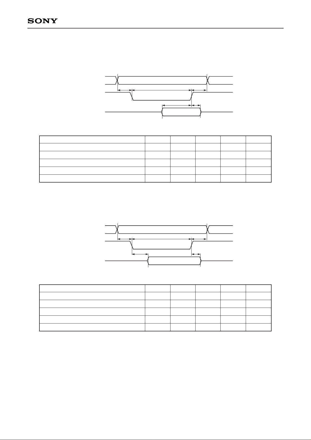
2. Memory interface
(1) Read
(2) Write
BA0 to 15
tRRLtSAO tHOA
tHOD
tSDO
XMOE
BDB0 to 7, P
Item
Address setup time (vs. XMOE ↓)
Address hold time (vs. XMOE ↑)
Data setup time (vs. XMOE ↑)
Data hold time (vs. XMOE ↑)
Low level XMOE pulse width
Symbol
tSAO
tHOA
tSDO
tHOD
tRRL
Min.
Tw–22
Tw–9
45
0
2 • Tw
Typ. Max.
2•Tw+16
Unit
n
n
n
n
n
BA0 to 15
t
WWL
tSAW tHWA
tFWD
tDWD
XMWR
BDB0 to 7, P
Item
Address setup time (vs. XMWR ↓)
Address hold time (vs. XMWR ↑)
Data delay time (vs. XMWR ↓)
Data float time (vs. XMWR ↑)
Low level XMWR pulse width
Symbol
tSAW
tHWA
tDWD
tFWD
tWWL
Min.
Tw–29
Tw–9
10
2 • Tw
Typ. Max.
0
Unit
n
n
n
n
n
Where Tw=1/f.
Usually, when f=16.9344 MHz, use a RAM with access time within 120 ns.
Page 9
—9—
CXD1186CQ/CR
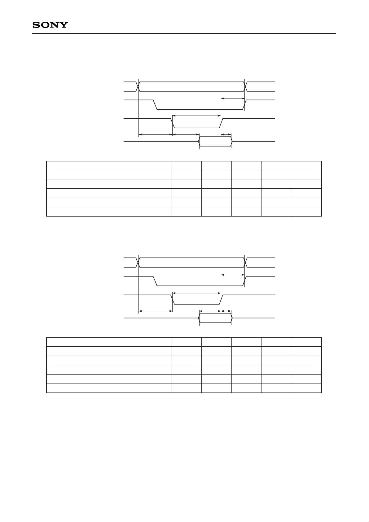
3. Host interface
(1) Read
(2) Write
HA0 to 1
tHRA
tRRL
tFRD
tDRDtSAR
XHCS
XHRD
HDB0 to 7, P
Item
Address setup time (vs. XHCS & XHRD ↓)
Address hold time (vs. XHCS & XHRD ↑)
Data delay time (vs. XHCS & XHRD ↓)
Data float time (vs. XHCS & XHRD ↑)
Low level XHRD pulse width
Symbol
tSAR
tHRA
tDRD
tFRD
tRRL
Min.
30
20
0
100
Typ. Max.
60
10
Unit
n
n
n
n
n
HA0 to 1
tSAW
tWWL
tSDW
tHWD
tHWA
XHCS
XHWR
HDB0 to 7, P
Item
Address setup time (vs. XHCS & XHWR ↓)
Address hold time (vs. XHCS & XHWR ↑)
Data setup time (vs. XHCS & XHWR ↑)
Data hold time (vs. XHCS & XHWR ↑)
Low level XHWR pulse width
Symbol
tSAW
tHWA
tSDW
tHWD
tWWL
Min.
30
20
40
10
50
Typ. Max. Unit
n
n
n
n
n
Page 10

—10—
CXD1186CQ/CR
4. HOST DMA cycle (80 type bus)
(1) Read
(2) Write
HDRQ
t
DAR2
tHRA
tRRL
tSAR
tDAR1
tDRD
tFRD
XHAC
XHRD
HDB0 to 7, P
Item
HDRQ fall time (vs. XHAC ↓)
HDRQ rise time (vs. XHAC ↑)
XHAC setup time (vs. XHRD ↓)
XHAC hold time (vs. XHRD ↑)
Low level XHRD pulse width
Data delay time (vs. XHRD ↓)
Data float time (vs. XHRD ↑)
Symbol
tDAR1
tDAR2
tSAR
tHRA
tRRL
tDRD
tFRD
Min.
5
0
100
0
Typ. Max.
35
48
60
10
Unit
n
n
n
n
n
n
n
HDRQ
t
SAW
tWWL
tHWA
tHWD
tSDW
tDAR1
tDAR2
XHAC
XHWR
HDB0 to 7, P
Item
HDRQ fall time (vs. XHAC ↓)
HDRQ rise time (vs. XHAC ↑)
XHAC setup time (vs. XHWR ↓)
XHAC hold time (vs. XHWR ↑)
Low level XHWR pulse width
Data setup time (vs. XHWR ↑)
Data hold time (vs. XHWR ↑)
Symbol
tDAR1
tDAR2
tSAW
tHWA
tWWL
tSDW
tHWD
Min.
5
0
50
40
10
Typ. Max.
35
48
Unit
n
n
n
n
n
n
n
Page 11

—11—
CXD1186CQ/CR
5. HOST DMA cycle (SCSI bus)
(1) Read
(2) Write
SDRQ
tDDA
tDAR
tRRL
tDRA
tHRD
tDRD
XSAC
XHRD
HDB0 to 7, P
Item
XSAC fall time (vs. SDRQ ↑)
XSAC delay time (vs. XHRD ↓)
XSAC delay time (vs. XHRD ↑)
Low level XHRD pulse width
Data delay time (vs. XHRD ↓)
Data hold time (vs. XHRD ↑)
Symbol
tDDA
tDAR
tDRA
tRRL
tDRD
tHRD
Min.
0
T+59
0
Typ. Max.
Tw
Tw
90
Unit
n
n
n
n
n
n
SDRQ
tDDA
tDAW tWWL tDWA
tFWD
tSDW
XSAC
XHWR
HDB0 to 7, P
Item
XSAC fall time (vs. SDRQ ↑)
XHWR delay time (vs. XSAC ↓)
XSAC delay time (vs. XHWR ↑)
Low level XHWR pulse width
Data setup time (vs. XHWR ↓)
Data float time (vs. XHWR ↓)
Symbol
tDDA
tDAW
tDWA
tWWL
tSDW
tFWD
Min.
T
T+24
27
Typ. Max.
Tw
Tw
Tw
Unit
n
n
n
n
n
n
Where T in the chart indicates :
Tw for 3 cycle mode
2 • Tw for 4 cycle mode
3 • Tw for 5 cycle mode
Here Tw=1/f
Page 12

—12—
CXD1186CQ/CR
6. ADPCM DMA cycle
Where T in the chart indicates :
Tw for 3 cycle mode
2 • Tw for 4 cycle mode
3 • Tw for 5 cycle mode
Here Tw=1/f
7. XTL1 and XTL2 pins
(1) For self oscillation (Topr=–20 to +75 °C, VDD=5.0 V±10 %)
(2) When a pulse is input to XTL1 (Topr=–20 to +75 °C, VDD=5.0 V±10 %)
ADRQ
tWWL tDWAtDAW
tDDA
tSDW
tFWD
XAAC
XHWR
HDB0 to 7, P
Item
XAAC fall time (vs. ADRQ ↑)
XHWR delay time (vs. XAAC ↓)
XAAC delay time (vs. XHWR ↑)
Low level XHWR pulse width
Data setup time (vs. XHWR ↓)
Data float time (vs. XHWR ↓)
Symbol
tDDA
tDAW
tDWA
tWWL
tSDW
tFWD
Min.
T
T+24
27
Typ. Max.
Tw
Tw
Tw
Unit
n
n
n
n
n
n
tW
tR tF
tWHX tWLX
tILX
VIHX
VIHX X0.9
VIHX X0.1
VDD/2
XTL1
Item
“H” level pulse width
“L” level pulse width
Pulse period
Input “H” level
Input “L” level
Rise time, Fall time
Symbol
tWHX
tWLX
tW
VIHX
VILX
tR, tF
Min.
15
15
40.7
VDD—1.0
Typ. Max.
0.8
15
Unit
ns
ns
ns
V
V
ns
Item
Oscillation frequency
Symbol
fMAX
Min.
16.9344
Typ. Max.
24.576
Unit
MHz
Page 13

—13—
CXD1186CQ/CR
Description of Function
1. Pin description
Below is a description of pins by function.
1.1 CD player interface (4 pins)
(1) DATA (input)
Serial data from CIRC LSI (digital signal processing LSI for CD)
(2) BCLK (input)
Bit clock. Clock for DATA Strobe.
(3) LRCK (input)
LR clock. Indicates LCH and RCH of DATA input.
(4) C2PO (positive logic input)
C2 pointer signal from CIRC. Indicates an error is included in the DATA input.
Interface mode with the CD player is controlled at DRVIF register.
1.2 Buffer memory interface (27 pins)
(1) XMWR (memory write, negative logic output)
Data write strobe signal of the buffer memory.
(2) XMOE (memory output enable, negative logic output)
Data read strobe signal of the buffer memory.
(3) BA0 to 15 (Buffer memory address, output)
Address signal of the buffer memory.
(4) BDB0 to 7 (Buffer data bus, I/O)
Data bus signal of the buffer memory.
(5) BDBP (Buffer data bus, I/O)
Buffer memory data bus signal for error pointer.
1.3 CPU interface (16 pins)
(1) XWR (CPU write, negative logic input)
Write strobe signal of the CPU register.
(2) XRD (CPU read, negative logic input)
Read out strobe signal of the CPU register.
(3) XCS (CPU chip select, negative logic input)
Chip select negative logic signal from the CPU.
(4) A0 to 3 (CPU address, input)
Address signal for the CPU selection of the IC internal register.
(5) DB0 to 7 (CPU data bus, I/O)
CPU data bus signal.
(6) INT (CPU interrupt, output)
Interrupt request output to the CPU. This pin polarity is controlled at the CONFIG register.
1.4 Host interface (19 pins)
(1) HMDS (Host mode select, input)
Signal for the host mode selection. This pin is pulled down inside the IC by means of a resistor at a
standard 50 kΩ.
“L” or open : connected to Intel 80 type host Bus.
“H” : connected to SCSI controller IC.
(2) HDRQ/XSAC (Host data request/SCSI acknowledge, output)
When HMDS is at “L”, DMA data request positive logic signal to host.
When HMDS is at “H”, DMA acknowledge negative logic signal to SCSI control IC.
Page 14

—14—
CXD1186CQ/CR
(3) XHAC/SDRQ (Host DMA acknowledge/SCSI data request, input)
When HMDS is at “L”, DMA acknowledge negative logic signal from host.
When HMDS is at “H”, DMA data request positive logic signal from SCSI control IC.
(4) XHWR (Host write, negative logic I/O)
When HMDS is at “L” and ADMAEN (DMACTL register, bit4) also at “L”, data write strobe input from
host.
When HMDS is at “H” and ADMAEN at “L”, data write strobe output to SCSI control IC.
When ADMAEN is at “H”, data write strobe output to audio processor (ADP).
(5) XHRD (Host read, negative logic I/O)
When HMDS is at “L” and ADMAEN also at “L”, data read strobe input from host.
When HMDS is at “H” and ADMAEN at “L”, data read strobe output to SCSI control IC.
When ADMAEN is at “H”, data read strobe output to ADP.
(6) XHCS (Host chip select, negative logic input)
This pin is pulled up inside the IC by means of a resistor at a standard 50 kΩ.
When HMDS is at “L”, chip select input from host.
When HMDS is at “H”, this signal is not used. Either fix to “H” or keep open.
(7) HA0 and 1 (Host address, input)
These pins are pulled up inside the IC by means of a resistor at a standard 50 kΩ.
When HMDS is at “L”, address input from the host.
When HMDS is at “H”, these signals are not used. Either fix to “H” or keep open.
(8) HDB0 to 7 (Host data bus, I/O)
Host data bus signal.
(9) HDBP (Host data bus, I/O)
Host data bus signal for error pointer.
(10) HINT (HOST interrupt, output)
This pin is an open drain output.
When HMDS is at “L”, interrupt request negative logic output to host.
When HMDS is at “H”, this signal is not used.
(11) XTC (Terminal count, negative logic output)
This is pulled up inside the IC by means of a resistor at a standard 50 kΩ.
When HMDS is at “L”, data transfer complete instruction negative logic input from the host.
When HMDS is at “H”, this signal is not used. Either fix to “H” or keep open.
1.5 Audio processor (ADP) interface (2 pins)
(1) ADRQ (audio processor DMA request, positive logic input)
This pin is pulled down inside the IC by means of a resistor at a standard 50 kΩ.
DMA data request signal to ADP. When not connected to ADP and CXD1186Q, either fix to “L” or keep
open.
(2) XAAC (audio processor DMA acknowledge, negative logic output)
DMA acknowledge signal from ADP.
1.6 Others (4 pins)
(1) XTL1 (Crystal1, input)
(2) XTL2 (Crystal2, output)
Crystal oscillator connecting pin for master clock oscillation.
(3) HCLK (halfclock, output)
Half frequency divided clock of the master clock.
(4) XRST (Reset, negative logic input)
Chip reset signal.
Pins BDB0 to 7, BDBP, DB0 to 7, HDB0 to 7 and HDBP are pulled up inside the IC by means of a
resistor at a standard 25 kΩ.
Page 15

—15—
CXD1186CQ/CR
2. Register function
This IC is controlled from the CPU by means of 19 registers for each of write and read, respectively.
2.1 Write register
2.1.1 Drive Interface (DRVIF) register
bit0 : DIGIN (Digital IN)
“H” ; When Digital In (See fig. 2.1.1) is connected, this bit is set to “H”.
“L” ; When connected to CIRC LSI, this bit is set to “L”.
bits 2 to 5 are effective only when DIGIN is at “L”.
bit1 : LSB1ST (LSB First)
“H” ; When data is connected to CIRC LSI output through LSB first, this bit is set to “H”.
“L” ; When data is connected to CIRC LSI output through MSB first, this bit is set to “L”.
bits2 and 3 : BCKMD 0, 1 (BCLK mode 0, 1)
These bits are set according to the number of BCLK clocks output during one word by CIRC LSI.
BCKMD 1 BCKMD 0
“L” “L” 16BCLKs/Word
“L” “H” 24BCLKs/Word
“H” “X” 32BCLKs/Word
Moreover, when there are 24 or 32 clocks within 1 word, the 16 bits of data before LRCK edge, become
effective.
bit4 : BCKRED (BCLK Rising Edge)
“H” ; Data is strobed with BCLK rise.
“L” ; Data is strobed with BCLK fall.
bit5 : LCHLOW (LCH LOW)
“H” ; When LRCK is at “L”, it is determined to be LCH data.
“L” ; When LRCK is at “H”, it is determined to be LCH data.
∗1. When DIGIN=“H”, We automatically have LSBIST=BCKMD1=“H”, BCKRED=LCHLOW=“L”.
bit6 : DBLSPD (Double Speed)
“H” ; At double speed PB, this bit is set to “H”.
“L” ; At normal speed PB, this bit is set to “L”.
bit7 : C2PLIST (C2PO Lower-byte 1st)
“H” ; When 2 bytes of data are input to C2PO, the Lower-byte and the upper-byte are input in the order.
“L” ; When 2 bytes of data are input to C2PO, the Upper-byte and the lower-byte are input in the order.
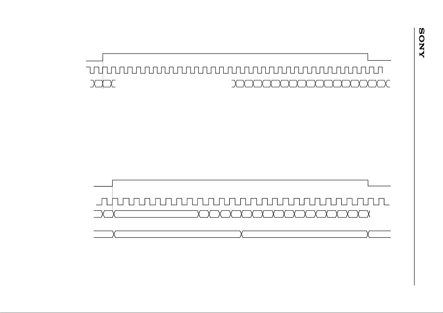
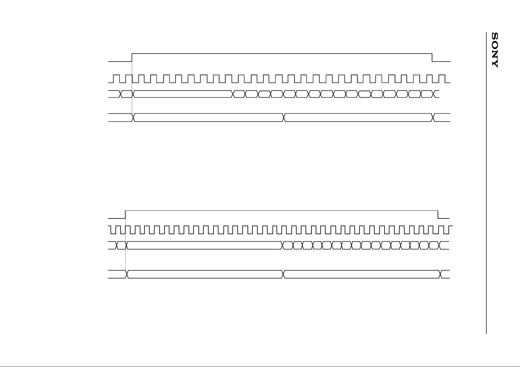
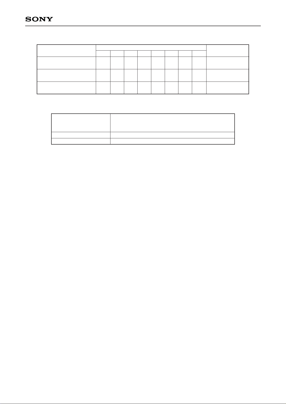
Table 2.1.1 indicates the setting value of bits 0 to 7 when Sony-made CIRC LSI is connected. Fig. 2.1.1 (1)
to (4) indicates the input timing chart.
Here, the upper byte means the upper 8 bits including MSB from CIRC LSI, Lower byte indicates the lower 8
bits including LSB from CIRC LSI.
Changes in value for the respective bits in this register have to be executed in the decoder disable condition.
Page 16
—16—
CXD1186CQ/CR
LRCK
BCLK
DATA
Rch Validity FLAG Rch LSB Rch • MSB
L0 RV
R15 R14 R13 R12 R11 R10 R9 R8 R7 R6 R5 R4 R3 R2 R1 R0 LV
1 2 3 4 5 6 7 8 9 10 11 12 13 14 15 16 17 18 19 20 21 22 23 24 25 26 27 28 29 30 31 32
Fig. 2.1.1 (1) Digital In Timing Chart (C2PO don’t care, no need for connection)
LRCK
BCLK
DATA
C2PO
Rch LSB Lch MSB Lch • LSB
C2 Pointer for Upper byte C2 Pointer for Lower byte
R0 L15 L14 L13 L12 L11 L10 L9 L8 L7 L6 L5 L4 L3 L2 L1 L0
1 2 3 4 5 6 7 8 9 101112131415161718192021222324
Fig. 2.1.1 (2) CDL30, 35 Series, Timing Chart
Page 17
—17—
CXD1186CQ/CR
LRCK
BCLK
DATA
C2PO
Rch LSB Lch MSB Lch LSB
C2 Pointer for Upper byte C2 Pointer for Lower byte
R1
R0 L15 L14 L13 L12 L11 L10 L9 L8 L7 L6 L5 L4 L3 L2 L1 L0
123456789101112131415161718192021222324
Fig. 2.1.1 (3) CXD2500Q, 48 bit Slot Mode Timing Chart
1234567891011121314151617181920212223242526272829303132
LRCK
BCLK
DATA
C2PO
Lch MSB Rch LSB Rch MSB
L14 L15 R0 R1 R2 R3 R4 R5 R6 R7 R8 R9
R10 R11 R12 R13 R14 R15
C2 Pointer for Upper byte C2 Pointer for Lower byte
Fig. 2.1.1 (4) CXD2500Q, 64 bit Slot Mode Timing Chart
Page 18
—18—
CXD1186CQ/CR
Table 2.1.1 DRVIF Register setting value
(Note 1) ∗ at normal speed PB set to “L”, at double speed PB set to “H”.
(Note 2)
2.1.2 Decoder Control (DECCTL) register
bits0 to 2 : DECMDSL2, 1, 0
(Decoder Mode Select 2, 1, 0)
DECMDSL2 1 0
“L” “L” “X” Decoder disable
“L” “H” “X” Monitor only mode
“H” “L” “L” Write only mode
“H” “L” “H” Real time correction mode
“H” “H” “L” Repeat correction mode
“H” “H” “H” CD-DA mode
bit3 : AUTODIST (Auto Distinction)
“H” ; Error Correction performed according to the Mode byte and FORM bit read from Drive.
“L” ; Error Correction is performed according to the following MODESEL and FORMSEL bits.
bit4 : FORMSEL (Form Select)
bit5 : MODESEL (Mode Select)
When AUTODIST is at “L” the sector is corrected as the following MODE or FORM.
MODESEL FORMSEL
“L” “L” MODE1
“H” “L” MODE2, FORM1
“H” “H” MODE2, FORM2
bit6 : ECCSTR (ECC Strategy)
“H” ; Error Correction is performed with consideration to respective data error flag.
“L” ; Error Correction is performed without consideration to respective data error flag. When an 8
bit/Word RAM is connected, turn this bit to “L”.
bit7 : ENDLADR (Enable DLADR)
“H” ; When this bit is set to “H”, DLADR is enabled.
When, either write only mode, real time correction, or CD-DA mode is being executed, the decoder
stops the buffer write as DADRC and DLADR turn equal.
“L” ; When this bit is set to “L”, DLADR is disabled.
During the execution of write only mode or real time correction, even if DADRC and DLADR turn
equal, the decoder does not stop buffer write.
(See paragraph 4 for details)
Sony-made CIRC LSI
CDL30 series
CDL35 series
CDL40 series
(48 bit slot mode)
CDL40 series
(64 bit slot mode)
DRV IF Register
bit7 bit6 bit5 bit4 bit3 bit2 bit1 bit0
L ∗ LLLHLL
L ∗ LHLHLL
L ∗ HLHXHL
Timing chart
Fig. 2.1.1 (2)
Fig. 2.1.1 (3)
Fig. 2.1.1 (4)
CDL30 series
CDL35 series
CDL40 series
CXD1125Q/QZ, CXD1130Q/QZ, CXD1135Q/QZ,
CXD1241Q/QZ, CXD1245Q, CXD1246Q/QZ,
CXD1247Q/QZ/R and others.
CXD1165Q, CXD1167Q/QZ/R and others.
CXD2500Q/QZ and others.
Page 19

—19—
CXD1186CQ/CR
2.1.3 DMA Control (DMACTL) register
bit0 : HSRC (Host Source)
“H” ; Data is transferred from the host to the buffer memory.
“L” ; Data is transferred from the buffer memory to the host.
bit1 : HDMAEN (HOST DMA Enable)
“H” ; DMA of the host port is enabled.
“L” ; DMA of the host port is prohibited.
bit2 : ENXTC (Enable XTC)
“H” ; DMA completion of the host port through XTC pin input is enabled.
“L” ; DMA completion of the host port through XTC pin input is disabled.
bit3 : ENHXFRC (Enable XHFRC)
“H” ; DMA completion of the host port through HXFRC is enabled.
“L” ; DMA completion of the host port through HXFRC is disabled.
bit4 : ADMAEN (ADP DMA Enable)
“H” ; DMA of the audio processor port is enabled.
“L” ; DMA of the audio processor port is prohibited.
Also, prohibits turning HDMAEN and ADMAEN simultaneously to “H”.
bit5 : CSRC (CPU Source)
“H” ; Data is transferred from the CPU to the buffer memory.
“L” ; Data is transferred from the buffer memory to the CPU.
bit6 : CDMAEN (CPU DMA Enable)
“H” ; DMA of the CPU port is enable.
“L” ; DMA of the CPU port is prohibited.
bit7 : RESERVED
Unused, Keep set to “L”.
2.1.4 Configuration (CONFIG) register
bit0 : RESERVED
Unused, Keep set to “L”.
bits1 and 2 : SDMACYC1, 0 (SCSI DMA CYCLE)
DMA transfer between this IC, SCSI control IC and ADPCM processor is executed in the
following cycle.
SDMACYC1 0
“L” “L” 3 cycle.
“L” “H” 4 cycle.
“H” “X” 5 cycle.
bit3 : SBSCTL (SCSI Bus Control)
Setting this bit to “H” forces XHWR, XHRD, HDB0 to 7 and HDBP into high impedance condition.
bit4 : CINTPOSI (CPU Interrupt Positive)
“H” ; INT pin turns to High active.
“L” ; INT pin turns to Low active.
bit5 : 9 BITRAM
“H” ; When a 9 bit/word RAM is connected, this bit is turned to “H”.
“L” ; When a 8 bit/word RAM is connected, this bit is turned to “L”.
bits6 and 7 : RESERVED
Unused, Keep set to “L”.
Page 20

—20—
CXD1186CQ/CR
2.1.5 Interrupt Mask (INTMSK) register
Turning the respective bits of the register to “H” enables interrupt request from this IC to the CPU by means
of the corresponding interrupt status. (That is, when interrupt status is turned on, INT pin is activated) The
value of the respective bits in this register does not affect the corresponding interrupt status.
bit0 : DECINT (Decoder interrupt)
When the Decoder is executing one of the respective modes, write only, monitor, or real time
correction, if Sync mark is detected or introduced, DECINT status is turned on. However, When
Sync detection window is open, if sync interval is less than 2352 bytes, Decint status is not
turned on.
Also, when Decoder repeat correction mode is being executed, everytime one correction is
completed DECINT status is turned on.
bit1 : HDMACMP (Host DMA Complete)
When DMA of the host port is completed through HXFRC or XTC pins, HDMACMP status is
turned on.
bit2 : DRVOVRN (Drive Over Run)
When ENDLADR bit (bit7) of DECCTL register is set to “H”, and the DECODER has executed
write only, real time correction mode or CD-DA mode, as DADRC and DLADR become equal,
DRVOVRN status is turned on.
However, in CD-DA mode, even when ENDLADR bit is turned to “L”, DRVOVRN status is turned
on.
bit3 : HSTCMND (Host Command)
As the host writes a command in the Command register, HSTCMND status is turned on.
bit4 : HCRISD (Host Chip Reset Issued)
By having the host write “H” in CHPRST bit (bit7) of the Control register, this IC is reset and
HCRISD status is turned on.
bit5 : RSLTEMPT (Result Empty)
When the host reads the Result register, and the Result register becomes empty, RSLTEMPT
status turns on.
bit6 : DECTOUT (Decoder Timeout)
After setting the Decoder to either, monitor only, write only or real time correction modes, if, even
after the time of three sectors (normal speed PB 40.6 ms) passes, sync is not detected, then
DECTOUT status is turned on.
2.1.6 Clear Interrupt Status (INTCLR) register
When any of the respective bits of this register is set to “H”, the corresponding interrupt status is cleared.
After the interrupt status clearance, the bit automatically turns to “L”. Accordingly there is no need for the
CPU to set to “L” again.
bit0 : DECINT (Decoder Interrupt)
bit1 : HDMACMP (Host DMA Complete)
bit2 : DRVOVRN (Drive Over Run)
bit3 : HSTCMND (Host Command)
bit4 : HCRISD (Host Chip Reset Issued)
bit5 : RSLTEMPT (Result Empty)
bit6 : DECTOUT (Decoder Timeout)
2.1.7 Drive • Last • Address • Low (DLADR-L) register
Page 21

—21—
CXD1186CQ/CR
2.1.8 Drive • Last • Address • High (DLADR-H) register
When the Decoder is executing either of write only, real time correction mode or CD-DA mode, CPU sets the
last address that writes into the buffer, data from the drive. When ENDLADR bit of DECCTL register is set to
“H” and the Decoder is executing the above modes, if data from the drive is written into the buffer at the
address specified from DLADR, all writing into the buffer is prohibited after that.
2.1.9 Drive • Address • Low (DADRC-L) counter
2.1.10 Drive • Address • Counter High (DADRC-H)
This counter keeps the address that writes data from the drive into the buffer. When drive data is written into
the buffer, DADRC contents are output form BA0 to 15. For every byte written in the buffer, DADRC is
incremented. Before the Decoder executes either write only, real time correction mode or CD-DA mode,
CPU sets the buffer write head address to DADRC.
This counter can also be used as the DMA address of the CPU port. During DMA execution of the CPU port,
DADRC contents are output from BA0 to 15, DADRC is incremented at every byte of DMA execution.
CPU can read or set DADRC contents at any time. Do not alter DADRC contents during either write only,
real time correction or CD-DA mode and the DMA execution of CPU port.
2.1.11 Host • Address • Low (HADRC-L) counter
2.1.12 Host • Address • High (HADRC-H) counter
This counter keeps the address that writes data from the host into the buffer or reads from the buffer. During
execution of the host port DMA, HADRC contents are output from BA0 to 15. The counter is incremented at
every DMA of the host port.
Before execution of the host port DMA, CPU sets the DMA head address to HADRC.
CPU can read or set HADRC contents at any time, Do no alter HADRC contents during host port DMA
execution.
2.1.13 Host • Transfer • Low (HXFRC-1) counter
2.1.14 Host • Transfer • High (HXFRC-H) counter
This counter indicates the number of host port DMA transfers. It is decremented at every host port DMA.
When ENHXFRC bit (bit3) of DMACTL register is set to “H” and HXFRC value turns to 0, the host port DMA
is disabled. At that time it is possible to send an interrupt request from this IC to the CPU.
CPU can read and set HXFRC contents at any time. Do not alter HXFRC contents during Host port DMA
execution.
2.1.15 Chip Control (CHPCTL) register
bit0 : CPUBWPO (CPU Buffer Write Pointer)
Sets the pointer value for CPU port DMA (buffer write).
bit1 : CHPRST (Chip Reset)
Setting this bit to “H” initializes the interior of this IC. After the initialization of the interior of this IC is
completed, this bit automatically turns to “L”. Accordingly it is not necessary to set the CPU to “L”.
bit2 : SWOPN (Sync Window Open)
“H” ; Setting this bit to “H” opens the window to allow for SYNC Mark detection. Sync protection circuit
inside this IC is disabled.
“L” ; Setting this bit to “L” controls the window through the sync protection circuit inside the IC.
bit3 : RPSTART (Repeat Correction Start)
Setting the Decoder to repeat correction mode and this bit to “H” starts the sector error
correction. As correction starts, this bit automatically turns to “L”. Accordingly it is not necessary
to set the CPU to “L”.
bits4 to 7 : Do not fail to set to “L”. If set to “H” IC operation is not guaranteed.
Page 22

—22—
CXD1186CQ/CR
2.1.16 CPU Buffer Write Data (CPUBWDT) register
With the CPU port DMA (buffer write), data is written into this register.
When CDMAEN of DMACTL register=CSRC=“H”, write into this register is subject to the request of CPU port
DMA (buffer wire). See paragraph 6 for details.
2.1.17 Host Interface Control (HIFCTL) register
When HMDS is at “L”, this register controls the hardware of the host interface.
bit0 : HINT #1 (Host Interrupt #1)
This bit value becomes the value of HINTSTS #1 (bit0) from STATUS register on the host side.
bit1 : HINT #2 (Host Interrupt #2)
This bit value becomes the value of HINTSTS #2 (bit1) from STATUS register on the host side.
bit2 : HINT #3 (Host Interrupt #3)
This bit value becomes the value of HINTSTS #3 (bit2) from STATUS register on the host side.
(Note) Once “H” is written, until bits 0 to 2 are cleared from the host or the chip is reset, keep at “H”.
It is not possible to access the register from the CPU and turn bits 0 to 2 from “H” to “L”.
Accordingly, to set any of these bits, it is not necessary to take into consideration the value of other
bits.
When HINTSTS bit #1 to 3 from HIFSTS register that corresponds to the above bits are at “H”, it is
prohibited to write “H” in the above bits.
Therefore, before the CPU writes “H” in the above bits HIFSTS register should be read, and
confirmation made that corresponding HINTSTS bits #1 to 3 are at “L”.
bits3 to 5 : RESERVED
Unused. Keep set to “L”. If set to “H” the IC operation is not guaranteed.
bit6 : CLRRSLT (Clear Result)
When this bit is set to “H”, the result register is cleared. When these register’s clearance is
completed, this bit automatically turns to “L”. Therefore, there is no need for the CPU to set back
to “L”.
bit7 : CLRBUSY (Clear, Busy)
When this bit is set to “H”, BUSYSTS bit of HINTSTS register is cleared. When these register’s
clearance is complete, this bit turns automatically turns to “L”. Therefore, there is no need for the
CPU to reset to L.
2.1.18 Drive Result (DRVRSLT) register
This register is utilized to transfer the command execution result to the host, when HMDS=“L”. This register
is composed of a 10 bytes FIFO. For details see 4.2.1.
2.1.19 Register Address (REGADR) register
bits0 to 6 : Do not fail to set to “L”. If set to “H” the IC operation is not guaranteed.
bit7 : REGADR0 (Register Address0)
This bit is used for the register address expansion.
2.2 Read out register
2.2.1 Current Minute Address Low (CMADR-L) register
2.2.2 Current Minute Address High (CMADR-H) register
Indicates the buffer memory address where the current sector (after correction is completed) Minute bytes
are written.
Page 23

—23—
CXD1186CQ/CR
2.2.3 Header (HDR) register
A three bytes register that indicates the current sector Header byte.
By reading address 0H successively 4 times the CPU can know the Header byte value of the current sector,
starting from the Minute byte.
2.2.4 Sub Header (SHDR) register
A three bytes register that indicates the current sector Sub Header byte.
By reading address 1H successively 4 times, the CPU can know the Sub Header byte value of the current
sector, starting from the File byte.
2.2.5 Header Flag (HDRFLG) register
Indicates the Header and Sub Header error pointer value.
2.2.6 Interrupt Status (INTSTS) register
The value of the respective bits in this register indicates the condition of the corresponding interrupt status.
The bit value of INTMSK register does not affect the above mentioned bits.
bit0 : DECINT (DECODER Interrupt)
bit1 : HDMACMP (Host DMA Complete)
bit2 : DRVOVRN (Drive Over Run)
bit3 : HSTCMND (Host Command)
bit4 : HCRISD (Host Chip Reset Issued)
bit5 : RSLTEMPT (Result Empty)
bit6 : DECTOUT (Decoder Timeout)
2.2.7 DECODER Status (DECSTS) register
bit0 : NOSYNC
Indicates that Sync Mark could not be detected and that SYNC was inserted.
bit1 : SHRTSCT (Short Sector)
Indicates the Sync Mark interval was within 2352 bytes. This sector does not execute ECC and
EDC.
bit2 : ECCOK (ECC OK)
Indicates there are no more errors from the header of the sector where error correction was
completed up to P Parity byte. (In FORM2, this bit turns to don’t care.)
bit3 : EDCOK
Indicates EDC check showed there were no errors.
bit4 : CORDONE (Correction Done)
Indicates that sector contains bytes that were error corrected.
bit5 : CORINH (Correction Inhibit)
Indicates there was an error flag at MODE (and FROM) bytes when AUTODIST bit of DECODER
register was turned to “H”. This sector does not execute ECC and EDC.
bit6 : ERINBLK (Erasure in Block)
Turns to “H” when C2 pointer from CIRC LSI stood in 1 byte or more of all the bytes, with the
exception of current sector Sync byte.
bit7 : EDCALL0 (EDC ALL ZERO)
This bit turns to “H” when there are no error flags in any of EDC parity bytes of current sector,
and the value is at 00H.
Page 24

—24—
CXD1186CQ/CR
2.2.8 MODE FORM (MDFM) register
This register is effective only during the execution of Real time correction mode or Repeated correction
mode.
bit0 : CFORM (Correction FORM)
bit1 : CMODE (Correction MODE)
These bits indicate whether this IC identified MODE and FORM in that sector and executed error
correction.
CMODE CFORM
“L” “L” MODE1
“H” “L” MODE2, FORM1
“H” “H” MODE2, FORM2
bits2 to 4 : RMODE0, 1, 2 (Raw MODE)
RMODE1, 0 : Indicates the lower 2 bits value of raw MODE byte.
RMODE2 : Indicate the logical sum of the upper 6 bits and pointer in raw MODE byte.
2.2.9 DMA Status (DMASTS) register
bit0 : CBFWRDY (CPU Buffer Write Ready)
This bit turns to “H” when data written from CPU into CPUBWDT register is written in the buffer
memory. As CPU writes the next data into CPUBWDT register, it turns to “L” until that data is
written into the buffer memory. Also, when CSRS is set to “H” and CDMAEN to “H” (DMACTL
register), this bit turns to “H”.
CPU confirms this bit is at “H” and writes in the data into CPUBWDT register.
bit1 : CBFRRDY (CPU Buffer Read Ready)
When data read from buffer memory is kept ready in CPUBRDT register, this bit turns to “H”.
When CPU reads CPUBRDT register out it turns to “L”.
CPU confirms this bit is at “H” and reads out data from CPUBRDT register.
bit2 : CBFRDPO (CPU Buffer Read Pointer)
Indicates the value of the pointer bit read from the buffer memory.
bit7 : REGADR (Register Address)
This bit indicates the value of bit7 from Register Address register.
2.2.10 DADRC-L counter
2.2.11 DADRC-H counter
2.2.12 HADRC-L counter
2.2.13 HADRC-H counter
2.2.14 HXFRC-L counter
2.2.15 HXFRC-H counter
2.2.16 CPU Buffer Read Data (CPUBRDT) register
CPU port DMA (buffer read) data is read out from this register.
When CDMAEN of DMACTL register is at “H” and CSRC at “L”, the read out of this register is set for the
DMA (buffer read) request of the next CPU port.
2.2.17 Host Parameter (HSTPRM) register
When HMDS is at “L”, this register is used to know the command parameter from the host. This register is
composed of a 10 bytes FIFO.
Page 25

—25—
CXD1186CQ/CR
2.2.18 Host Command (HSTCMD) register
When HMDS is at “L”, this register is used to know the command from the host.
2.2.19 Host Interface Status (HIFSFS) register
When HMDS is at “L”, this register is used to know the host interface condition.
bit0 : HINTSTS #1 (HOST Interrupt Status #1)
This bit turns to “H” as CPU writes “H” into HINT #1 (HIFCTL register bit0). It turns to “L” when
the host writes “H” into CLRINT #1 (Control register bit0). This bit is used as interrupt status
monitor to the host.
bit1 : HINTSTS #2 (HOST Interrupt Status #2)
This bit turns to “H” as CPU writes “H” into HINT #2 (HIFCTL register bit1). It turns to “L” when
the host writes “H” into CLRINT #2 (Control register bit1). This bit is used as interrupt status
monitor to the host.
bit2 : HINTSTS #3 (Host Interrupt Status #3)
This bit turns to “H” as CPU writes “H” into HINT #3 (HIFCTL register bit2). It turns to “L” when
the host writes “H” into CLRINT #3 (Control register bit2). This bit is used as interrupt status
monitor to the host.
bit3 : PRMRRDY (Parameter, Read Ready)
This bit at “H” indicates that HSTPRM register is not empty, so that Parameter data can be read
out from the CPU. When this bit is at “L”, HSTPRM register is empty and Parameter data cannot
be read out from the CPU.
bit4 : PRMFULL (Parameter Full)
This bit at “H” indicates HSTPRAM register is full.
bit5 : RSLWRDY (Result Write Ready)
This bit at “H” indicates that DRVRSLT register is not full, so that the CPU can write Result data.
When this bit is at “L” DRVRSLT register is full and the CPU can not write Result data.
bit6 : RSLEMPT (Result Empty)
This bit at “H” indicates DRVRSLT register is empty.
bit7 : BUSYSTS (Busy Status)
This bit has the same value as that of BUSYSTS (bit7) of the status register on the host side.
This bit turns to “H” as the host writes a command in the Command register. It turns to “L”, as the
CPU sets CLRBUSY bit of HIFCTL register.
Page 26
—26—
CXD1186CQ/CR
∗∗∗∗∗ Write register ∗∗∗∗∗
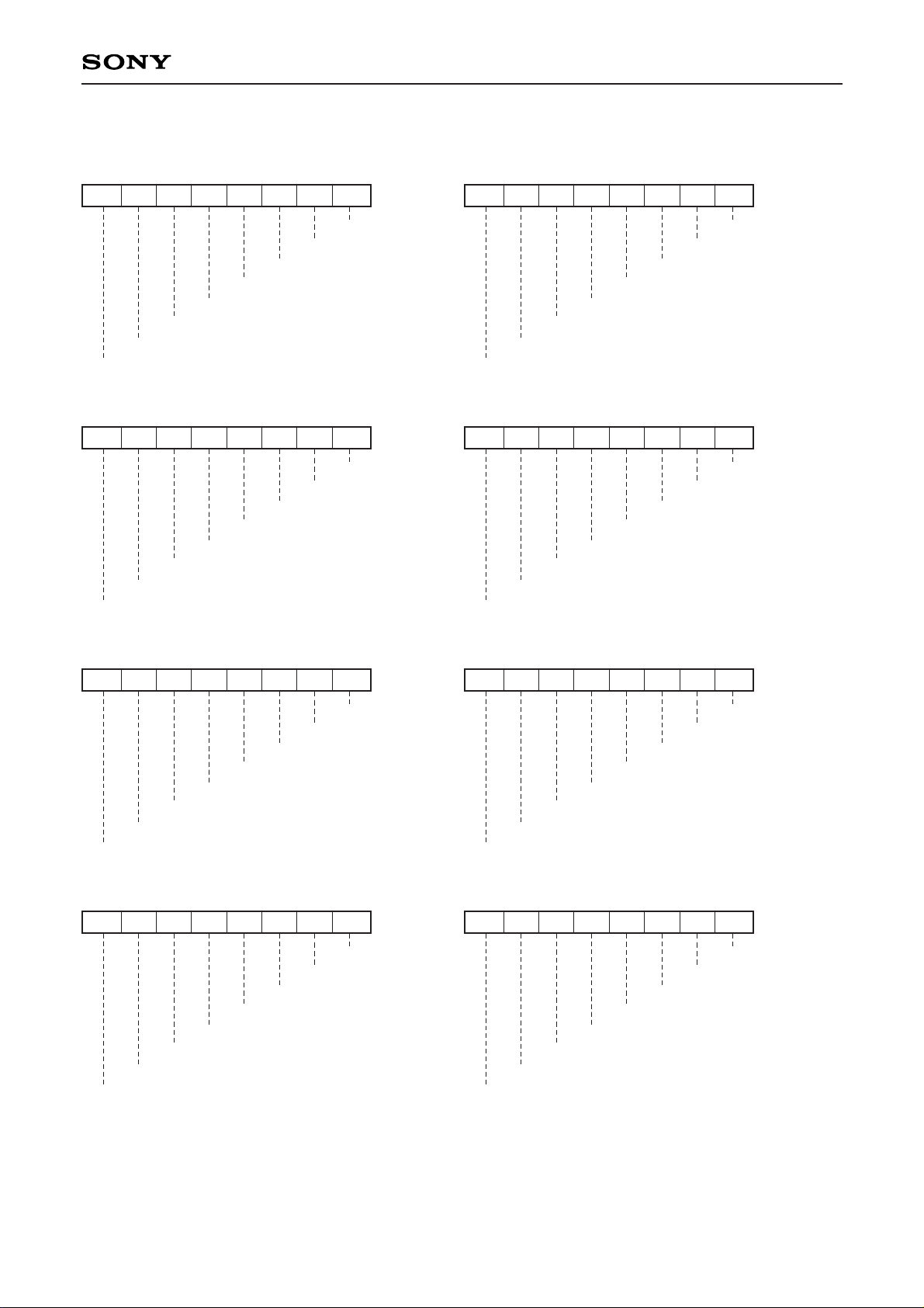
Drive Interface (DRVIF) DECODER Control (DECCTL)
DIGIN DECMDSL0
LSB1ST DECMDSL1
BCKMD0 DECMDSL2
BCKMD1 AUTODIST
BCKED FORMSEL
LCHLOW MODESEL
DBLSPD ECCSTR
C2PL1ST ENDLADR
DMA Control (DMACTL) Configuration (CONFIG)
HSRC RESERVED “L”
HDMAEN SDMACYC0
ENXTC SDMACYC1
ENHXFRC SBSCTL
ADMAEN CINTPOSI
CSRC 9BITRAM
CDMAEN RESERVED “L”
CORWRIDS RESERVED “L”
Interrupt Mask (INTMSK) Clear Interrupt Status (INTCLR)
DECINT DETINT
HDMACMP HDMACMP
DRVOVRN DRVOVRN
HSTCMD HSTCMD
HCRISD HCRISD
RSLTEMPT RSLTEMPT
DECTOUT DECTOUT
Chip Control (CHPCTL) Host Interface Control (HIFCTL)
CPUBWPO HINT#1
CHPRST HINT#2
SWOPN HINT#2
RPSTART “L”
“L” “L”
“L” “L”
“L” CLRFIFO
“L” CLRBUSY
76543210 76543210
76543210 76543210
76543210
76543210
76543210
76543210
Page 27
—27—
CXD1186CQ/CR
Register Address (REGADR)
“L”
“L”
“L”
“L”
“L”
“L”
“L”
REGADR
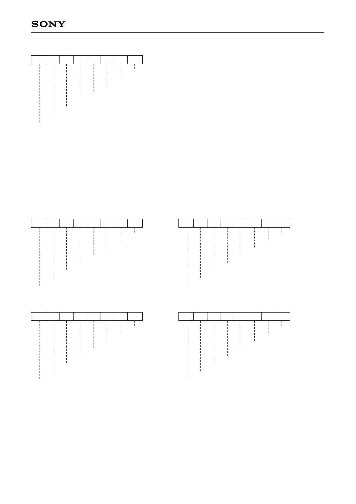
∗∗∗∗∗ Read register ∗∗∗∗∗
Header Flag Interrupt Status
DTTYPE DECINT
SUBMODE HDMACMP
CHANNEL DRVOVRN
FILE HSTCMD
MODE HCRISD
BLOCK RSLTEMPT
SECOND DECTOUT
MINUTE
DECODER Status MODEFORM
NOSYNC CFORM
SHRTSCT CMODE
ECCOK RMODE0
EDCOK RMODE1
CORDONE RMODE2
CORINH
ERINBLK
EDCALLO
76543210
76543210 76543210
76543210 76543210
Drive • Last • Address • Low
Drive • Last • Address • High
Drive • Address • Counter • Low
Drive • Address • Counter • High
Host • Transfer • Counter • Low
Host • Transfer • Counter • High
Host • Address • Counter • Low
Host • Address • Counter • High
CPU Buffer Write register
Drive Status register
Register Address register
Page 28

—28—
CXD1186CQ/CR
DMA Status Host Interface Status
CBFWRRDY HINT#1
CBFRDRDY HINT#2
CBFRDPO HINT#3
PRMRRDY
PRMFULL
RSLWRDY
RSLEMPT
REGADR BUSYSTS
Header register
Sub Header register
Current • Minute • Address • Low
Current • Minute • Address • High
Drive • Last • Address • Low
Drive • Last • Address • High
Drive • Address • Counter • Low
Drive • Address • Counter • High
Host • Transfer • Counter • Low
Host • Transfer • Counter • High
Host • Address • Counter • Low
Host • Address • Counter • High
CPU • Address • Counter • Low
CPU • Address • Counter • High
CPU Buffer Read register
Host Command register
Host Parameter register
76543210 76543210
Page 29

—29—
CXD1186CQ/CR
CXD1186Q register
ADDRESS
0
1
2
3
4
5
6
7
8
9
A
B
C
D
E
F
Write Read
REGISTER-ADDRESS REGISTER-ADDRESS
LHLH
DRVIF CONFIG HDR
DECCTL SHDR
DMACTL HDRFLG
INTMSK MODEFORM
INTCLR DECSTS
DLADR-L INTSTS
DLADR-H DMASTS
DADRC-L
DADRC-H
HXFRC-L
HXFRC-H TEST2
HADRC-L TEST1
HADRC-H TEST0
CPUBWDT HIFCTL CPUBRDT HSTCMD
CHPCTL DRVRSLT CMADR-L HSTPRM
REGADR CMADR-H HIFSTS
3. DECODER Operation
Here after, the block containing functions 1 and 2 is called DECODER.
1 Interface with CIRC LSI
The data stream from CIRC LSI is taken in, while sync detection, descramble and data write to the
buffer are executed.
2 Error correction
Executes error correction of the sector written in the buffer.
3.1 DECODER operation mode
The Decoder features 4 operation modes set by means of DECMDSEL0 to 2 bits of DECCTL register.
DECMDSL2 1 0
“L” “L” “X” Decoder disable
“L” “H” “X” Monitor only mode
“H” “L” “L” Write only mode
“H” “L” “H” Real time correction mode
“H” “H” “L” Repeat correction mode
“H” “H” “H” CD-DA mode
(1) Decoder disable
DECODER operation is disabled.
(2) Monitor only mode
Data from the drive is not written in the buffer. Raw data from the drive is written in the Header, Sub
Header and HDRFLG registers.
(3) Write only mode
Set to this mode, first Sync pattern detection is performed. As sync pattern is detected, write from that
sector into the buffer starts from Minute byte. The buffer memory address of this Minute byte, is the
value set to DADRC though the CPU before setting the DECODER mode. Sectors after that, and the
Sync pattern too, are written into the buffer.
This buffer write continues until either Decoder is disabled or when ENDLADR is at “H”, DLADR value
becomes equal to that of DADRC.
Page 30

—30—
CXD1186CQ/CR
(4) Real time correction mode
Buffer write works the same as write only mode.
At the same time, error correction of the sectors already written in the buffer is executed in real time.
(When this mode is set and while the first sector is being written in the buffer, as long as a whole sector
is not yet stored in the buffer, correction is not executed.)
(5) Repeat correction mode
Data from the drive is not written in the buffer. Error Correction of sectors already written in the buffer
can be executed repeatedly. This way, errors that could not be corrected during real time correction
mode, can now be corrected.
(6) CD-DA mode
To write CD-DA (Digital audio) Disc data into the buffer, this mode is set. As this mode is set, write into
the buffer is executed from the lower byte of LCH.
This buffer write continues until either Decoder is disabled, or when ENDLADR is at “H”, DLADR value
becomes equal to that of DADRC.
3.2 DADRC (Drive Address Counter)
DADRC is the counter that holds the address when data from the drive is written into the buffer. When data
from the drive is written into the buffer, the contents are output from BA0 to 15 as buffer memory address.
CPU can set or read DADRC contents. CPU sets the buffer write head address in DADRC before the setting
of Decoder write only mode, real time correction mode and CD-DA mode.
3.3 DLADR (Drive Last Address)
DLADR is the register that indicates in bytes the value of DADRC that stops the drive data buffer write during
the execution of write only mode, real time correction mode and CD-DA mode. When ENDLADR bit of
DECCTL register is at “H” and the above modes are being executed, if DADRC value becomes equal to
DLADR, it stops the buffer write data from the drive. Then, DRVOVRN status is on. When sync interrupt
applies and DRVOVRN bit is at “H”, have CPU disable the DECODER. When ENDLADR bit is at “L”, even if
DADRC value becomes equal to DLADR, buffer write of the data from the drive is not stopped and
DRVOVRN status does not turn on.
Through the usage of DLADR, buffer overran of the drive can be prevented.
When a value is set to DLADR, make sure to set the upper byte first and the lower byte next in the order.
(Even in case only the value of one of bytes is to be changed, set both bytes in the mentioned order. If this is
not performed, IC operation can not be guaranteed.) The DLADR upper byte is first set then the lower byte is
set and until data from the drive is written in the buffer, the above function is disabled. DLADR setting should
be made carefully.
3.4 Error correction
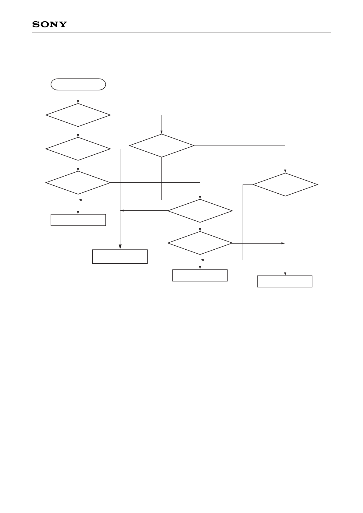
(1) MODE and FORM discrimination
Mode and Form discrimination in the sector that performs error correction is executed in bits
AUTODIST, FORMSEL and MODESEL of DECCTL register, as indicated in Fig. 3.1.
Page 31

—31—
CXD1186CQ/CR
(2) ECC strategy can be chosen through ECCSTR bit of DECCTL register.
At “H”, error correction is performed taking into consideration error flags from respective data.
At “L”, error correction is performed without taking into consideration error flags from respective data.
For systems using 8 bit word RAM, turn ECCSTR to “L”.
When double speed PB is executed (DBLSPD of DRVIF register is at “H”), transfer speed to the host
slows down. Data transfer speed to the host when XTL1 frequency is set to 16.9344 MHz is shown
below, Moreover, this data transfer speed is the value obtained when data buffer write from the drive,
error correction and data transfer to the host are executed at the same time.
From the above table, it appears that during double speed PB, data transfer speed to the host
decreases. During double speed PB, Read data speed from the Drive is at 352.8 KB/S. Data transfer
speed to the host at 0.7 MB/S is quite faster than this Read speed. Actually, transfer speed to the host
does not decrease and as Read data speed from the Drive doubles, transfer speed to the host also
approximately doubles.
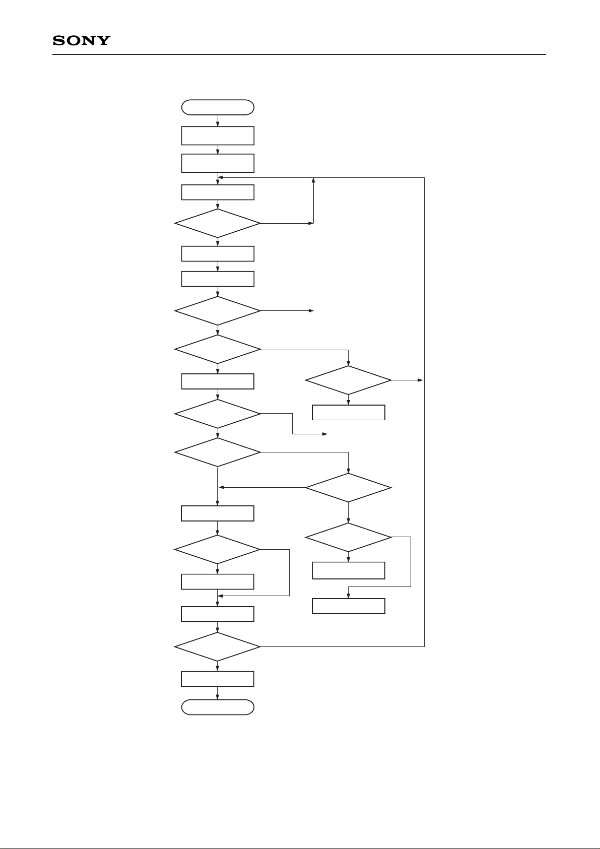
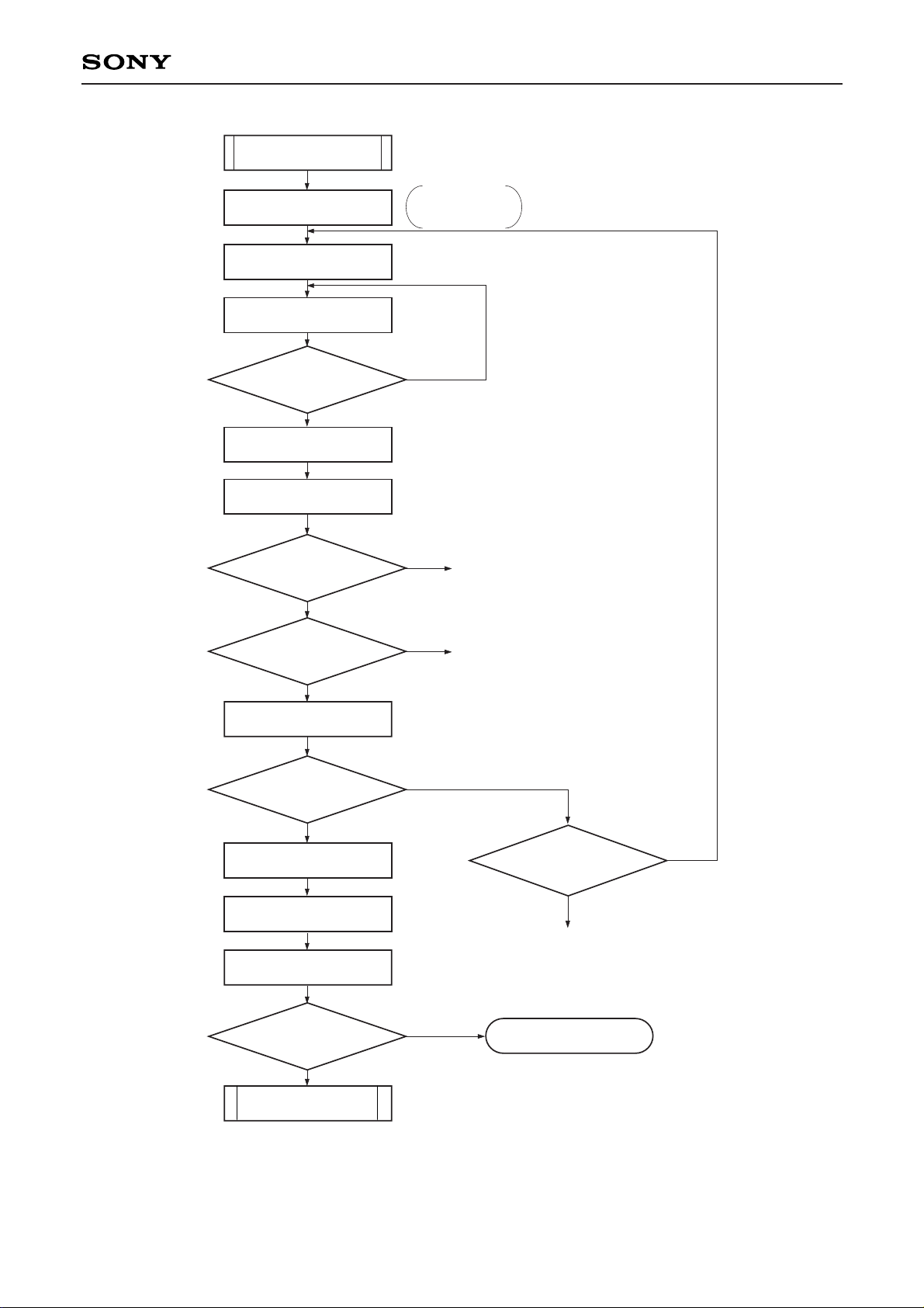
3.5 CPU control of the IC during Real time correction
CPU control of the IC during the IC execution of Real time correction mode is shown in Fig. 3.2.
3.6 CPU control of the IC during Repeat correction
CPU control of the IC during the IC execution of Repeat correction mode is shown in Fig. 3.3.
Normal PB speed
Double PB speed
ECCSTR
L
H
L
H
Data Transfer Speed
2.1 MB/S
0.7 MB/S
Page 32
—32—
CXD1186CQ/CR
START
Auto Dist
= “1” ?
Raw Mode
Error
N
N
N
N
N
N
Y
Y
Y
Y
Y
Y
Y
Raw Mode 1
?
Mode 1 correction
Mode Set
= “0” ?
Set
Corinh = “H”
Raw Sub
Mode Error?
Form 1
Form 1 correction
Form Set
= “0”
Form 2 correction
Fig. 3.1 MODE FORM Discrimination method
Page 33
—33—
CXD1186CQ/CR
START
SET DADRC
DLSTADR
SET DECCTL : (Real
time correction mode)
RD INTSTS
DEC Interrupt
status ?
Clear DEC Interrupt
RD HDR, HDRFLG
Header
Error in byte
Target sector ?
RD DECSTS
SHRTCST
Y
Y
Y
Y
Y
Y
Y
N
N
N
N
Seek
necessary
DECODER disable
N
N
Error in
current sector
Transfer to Host ?
RD CMADR
Repeated
correction
Repeated
correction
RETRY
N
N
N
Y
Y
DRVOVRN ?
DECODER disable
Transfer to Host
All sectors
decode ?
DECODER disable
END
Fig. 3.2 CPU control of the IC during real time correction
Page 34
—34—
CXD1186CQ/CR
Repeat
correction
SET DECCTL
SET CHPCTL
RD INTSTS
DEC Interrupt
status
Clear DEC Interrupt
RD HDR, HDRFLG
Error in
Header byte?
Target sector
RD DECSTS
Error in
current sector?
RD CMADR
DECODER disable
Transfer to Host
All sectors
decode
Decode
remaining sector
END
One more
correction?
Y
Y
Y
Y
Y
N
N
N
N
N
Repeat
correction mode
(RPSTART)
Fig. 3.3 CPU control of the IC during repeated correction
Page 35

—35—
CXD1186CQ/CR
4. Host interface
4.1 Host I/F mode
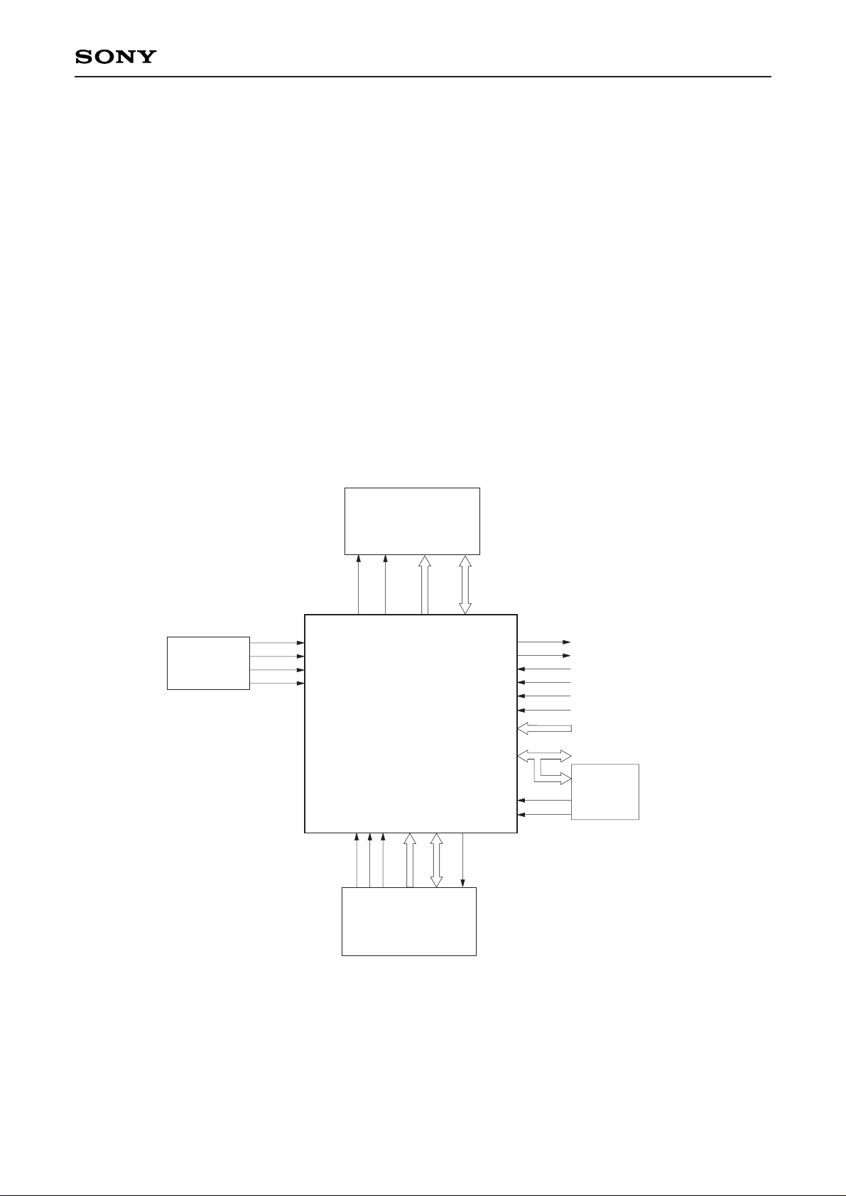
This IC can be connected to the following, as the host interface.
1 SCSI controller IC (CXD1180, CXD1185 and others)
2 Intel 80 type host bus
This mode is set by means of HMDS pin, as shown below.
When Intel 80 type host bus is connected, HMDS input is at “L”. Otherwise, HMDS pin is set to open.
When SCSI control IC is connected, HMDS input is at “H”.
4.2 Connected to Intel 80 type host bus
When this IC is connected to Intel 80 type host bus either “L” is input to pin HMDS or it is left open. This
connection is shown an Fig. 4.1.
4.2.1 Command/Status transfer between the Host and the CPU.
(1) Register
The host can access each of the 4 write and read registers. Using pins XHCS, HA0, HA1, XHRD and
XHWR, it reads and writes their registers. DMA transfer is also possible with RDDATA and WRDATA
registers despite XHCS, HA0 and HA1 values. Their registers are selected by means of XHAC, XHRD,
XHWR and DMA transfers performed with the host. Parameter register and Result register are 10 bytes
FIFO registers. “L” input to XHAC and XHCS is prohibited at the same time.
∗Write register
• Command register (address 0)
The host writes commands in this register. As the host writes in this register, interrupt request is applied
from this IC to the CPU. Bit assignment and function attribution is performed by means of a control
program.
• Parameter register (address 1)
To execute commands, the host writes into this register command parameters. This is a 10 bytes FIFO
register.
• Write Data (WRDATA) register (address 2)
This register serves to write data from the host into the buffer memory. Data can be written into either I/O
mode or DMA mode. This register is composed of a 2 × 9 bits FIFO.
• Control register (address 3)
This register is for the direct control of the hardware in this IC by the host.
bits0 to 2 : INTCLR #1 to 3 (Clear Interrupt #1 to 3)
Setting these bits to “H” will clear the corresponding interrupt status, After the clearance of
interrupt status in these bits, they automatically go back to “L”.
bits3 to 5 : ENINT #1 to 3 (Enable Interrupt #1 to 3)
Setting these bits to “H” will enable the corresponding interrupt status.
The host can read the respective bits value from the status register.
When the corresponding interrupt status is at “H”, it is prohibited to write “H” to these bits,
accordingly, before the host sets these bits to “H”, the Status register should be read out and
interrupt status confirmed.
bit6 : CLRPRM (Clear FIFO)
Setting this bit to “H” clears the Parameter register, After these registers are cleared, this bit
automatically goes back to “L”.
bit7 : CHPRST (Chip Reset)
Setting this bit to “H” initializes the inside of this IC. As the inside of this IC initialization is
completed, this bit automatically return to “L”. Setting this bit to “H” enables interrupt request to
the CPU.
Page 36

—36—
CXD1186CQ/CR
∗Read out register
• Status register (Address 0)
The host uses this register to read this IC status.
bits0 to 2 : INTSTS #1 to 3 (Interrupt Status #1 to 3)
The value of the respective bits is the same as that of the bits corresponding to HIFCTL register
of the sub CPU. When interrupt corresponding to the respective bits is enabled, they turn to “H”
and interrupt request to the host is output.
bits3 to 5 : ENINTST #1 to 3
(Enable Interrupt Status #1 to 3)
The value of the respective bits is the same as that of the bits corresponding to Control register.
bit6 : DREQSTS (Data Request Status)
Indicates this IC is in buffer memory data transfer request condition versus the host. This bit has
the same value as that of pin HDRQ. In I/O mode, when buffer memory data transfer is
executed, access WRDATA register or RDDATA register after the host confirms this bit is at “H”.
bit7 : BUSYSTS (Busy Status)
This bit turns to “H” as the Host writes a command into the Command register. It turns to “L” as
the sub CPU sets CLRBUSY bit of HIFCLT register.
• Result register (address 1)
The host reads the results after the command execution from this register.
This is a 10 bytes FIFO.
• Read Data (RDDATA) register (address 2)
This register is for the host to read data from the buffer memory. Data can be read in I/O mode or DMA
mode. It is composed of a 2 × 9 bits FIFO.
• FIFO Status register (address 3)
This register is for the host to read the status of Parameter or Result register.
bit0 : PRMWRDY (Parameter Write Ready)
When this bit is at “H” it indicates that Parameter register is not full, and that the host can write
parameter data.
bit1 : PRMEEMPT (Parameter Empty)
This bit at “H” indicates Parameter register is empty.
bit2 : RSLRRDY (Result Read Ready)
This bit at “H” indicates that Result register is not empty, and that the host can read Result data.
bit3 : RSLFULL (Result Full)
This bit at “H” indicates Result register is full.
bit4 to 7 : RESERVED
Unused.
Address
0
1
2
3
Write
Command
Parameter
Write Data
Control
Read
Status
Result
Read Data
FIFO Status
Page 37

—37—
CXD1186CQ/CR
Control Status
CLRINT#1 INTSTS#1
CLRINT#2 INTSTS#2
CLRINT#3 INTSTS#3
ENINT#1 ENINTSTS#1
ENINT#2 ENINTSTS#2
ENINT#3 ENINTSTS#3
CLRFIFO DREQSTS
CHPRST BUSYSTS
FIFO Status
PRMWRDY
PRMEMPT
RSLRRDY
RSLFULL
76543210 76543210
76543210
Page 38

—38—
CXD1186CQ/CR
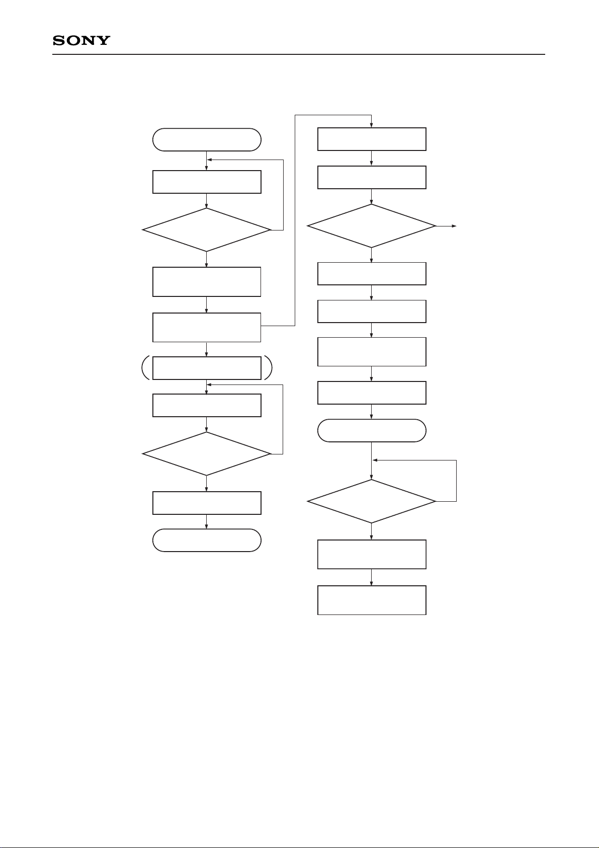
(2) Host and CPU controlling order
An example of the host and CPU controlling order is shown in Fig. 4.2.1.
In this case the host gets to know interrupt status by polling Status register, Interrupt request can also be
enabled.
4.2.2 Data transfer between the host and the buffer memory.
Data transfer between the host and the buffer memory is executed through this IC. This IC incorporates a 2
× 9 bits FIFO (WRDATA, RDDATA registers) to speed up data transfer.
(1) Data transfer in DMA mode
Data transfer between the host and FIFO inside this IC, is performed through handshake utilizing
HDRQ/XSAC and XHAC/SDRQ.
HDRQ/XSAC becomes the HDRQ data transfer request signal from this IC to the host while
XHAC/SDRQ becomes the corresponding acknowledge signal XHAC.
1 Data transfer from the host to the buffer memory (HSRC at “H”)
When HDMAEN is at “H” while FIFO in not full and XHAC is at “H”, this IC activates HDRQ. As
acknowledge signal XHAC comes back from the host, HDRQ is inactivated. With the rising edge of
XHAC, data is written into FIFO. Data written into FIFO is written in the buffer memory address in the
order prescribed by HADRC.
2 Data transfer from the buffer memory to the host (HSRC at “L”)
When HDMAEN is at “H”, buffer read data from the address prescribed by HADRC is written into the
FIFO. As data is written into FIFO, if XHAC is at “H”, this IC activates HDRQ. As the acknowledge
XHAC comes back from the host, HDRQ is inactivated. During the period when XHAC is at “L”, this IC
outputs the FIFO data to HDB0 to 7.
(2) Data transfer in I/O mode
The host can transfer data to and from the buffer memory, by writing or reading registers WRDATA and
RDDATA. In this case the control of CXD1186Q by the CPU is the same as during DMA transfer mode.
Fig. 4.2.2 indicates the host control flow when data transfer is performed in I/O mode between the host
and the buffer memory.
(3) Data transfer completion
The 3 following methods are for data transfer completion.
• HXFRC is used.
• XTC pin is used.
• HDMAEN bit is set to “L”.
1 When HXFRC is used:
When HXFRC is used for data transfer completion, perform the following before the CPU starts data
transfer.
• Set the number of data transfer bytes at HXFRC.
• Set the data transfer direction (HSRC bit) to “H” or “L” and ENHXFRC=HDMAEN to “H”. This
starts data transfer.
HXFRC is decremented every time data is written into FIFO.
When HXFRC turns to 0, writing of data into FIFO after that is not performed. Then, when all the FIFO
data is transferred to the buffer memory or the host, HDMACMP status (DMASTS register) sets on.
When HDMACMP bit of INTMSK register is set to “H”, this IC outputs interrupt request (INT output) to
the CPU.
2 When XTC pin is used
When XTC pin is used for data transfer completion, perform the following before the CPU starts data
transfer.
• Set the data transfer direction (HSRC bit) to “H” or “L” and ENXTC=HDMAEN to “H”. This starts
data transfer.
Page 39

—39—
CXD1186CQ/CR
During the host final DMA byte transfer, turn pin and XHAC, XHWR, XHRD to “L”. This way, data
transfer to the host is no more performed. (HDRQ is not output to the host.) When HSRC is at “L” and
XTC turns to “L”, after XHAC becomes inactive, this IC turns to HDMACMP status. In this case, 1 byte
of unnecessary data from the buffer memory may already be written in the FIFO.
Then, care should be exercised as the last address of HADRC transfer +2 is indicated. When HSRC
is at “H”, the IC turns to HDMACMP status, when the writing into the buffer memory of data written into
the FIFO as XTC at “L”, is completed.
In either case, as HDMACMP status sets on, and HDMACMP bit of INTMSK register is set to “H”, this
IC output interrupt request (INT output) to the CPU.
Both ENXTC and ENHXFRC bits of DMACTL register, can simultaneously be set to “H”.
(Note) In either 1 or 2 case, after HDMACMP sets on, before starting up data transfer again, turn bit 1
of INTCLR register to “H” and clear HDMACMP status.
3 When HDMAEN bit is set to “L”
When HDMAEN bit is set to “L” during data transfer with the host, data transfer is stopped. Then, data
transfer between this IC and the host or the buffer memory may be stopped half-way. The value of
HADRC and HXFRC after that is not guaranteed. Also, in this case, HDMACMP status does not set on.
(4) CPU control of the IC
CPU control of the IC when data transfer is performed between the host and the buffer memory is
illustrated as follows. (In this example execute data transfer completion using HXFRC)
1 The number of transfer bytes is set to HXFRC.
2 HADRC is set at the DMA head address.
3 Set the data transfer direction to “H” or “L” and HDMEAN and ENHXFRC bits of DMACTL register to
“H”.
4 As the transfer of the specified number of bytes is completed, HDMACMP bit of DMASTS register
turns to “H”. (Then, this IC can output an interrupt request to the CPU)
5 Also, HXFRC is at 0000H, while HADRC value stands as the value next to that of the buffer memory
address transferred last.
4.3 When connected to SCSI control IC
When this IC is connected to SCSI control IC, HMDS pin is set to “H”.
4.3.1 Connection method to SCSI control IC
• An example for the connection of this IC to an SCSI control IC where CPU bus and DMA bus are not
separated (ex. CXD1180AQ) is shown in Fig. 4.3.1.
To switch CPU and DMA buses, an external circuit is required.
• An example for the connection of this IC to an SCSI control IC where CPU and DMA buses are
separated (ex. CXD1185AQ) is shown in Fig. 4.3.2.
4.3.2 Data transfer between SCSI control IC and the buffer memory
Data transfer between SCSI control IC and buffer memory is performed through this IC.
(1) Data transfer handshake
XHAC/SDRQ become the data transfer request signal SDRQ from SCSI control IC to this IC.
HDRQ/XSAC become the corresponding acknowledge signal XSAC.
1 Data transfer from SCSI control IC to this IC (HSRC at “H”)
When HDMAEN is at “H”, SDRQ input while FIFO is not full will make this IC activate XSAC. Data is
written into FIFO with the rising edge of XHWR.
2 Data transfer from this IC to SCSI control IC (HSRC at “L”)
When HDMAEN is at “H”, SDRQ input while FIFO is not empty will make this IC activate XSAC. It
also outputs data from FIFO to HDB0 to 7 during the period XHAC is at “L”.
Page 40
SRAM
CXD2500Q
CPU
CXD1186CQ/CR
ADPCM
DECODER
ADRQ
XAAC
DATA
BCLK
LRCK
C2PO
XMWR
XMDE
BA0–15
BDB0–7,P
XWR
XRD
XCS
A0–3
DB0–7
INT
80 type host bus
HMDS = “L”
XHIN
HDRQ
XHAC
XHWR
XHRD
XHCS
HA0, 1
HDB0-7, P
Fig. 4.1 CXD1186CQ/CR connection (80 type host bus)
—40—
CXD1186CQ/CR
(2) Completion of data transfer
The 2 following methods are for the completion of data transfer.
• HXFRC is used.
• HDMAEN is set to “L”.
For either method refer to paragraph 4.2.2.
(3) Data transfer cycle
The data transfer cycle between this IC and SCSI control IC can be controlled through SDMACYC 0 and
1 bits from CONFIG register. CPU sets these bits in coordination with the speed of SCSI control IC
(See A.C characteristics)
SDMACYC1 0
“L” “L” 3 cycles.
“L” “H” 4 cycles.
“H” “X” 5 cycles.
(4) CPU control of the IC
For CPU control of the IC when data transfer is executed between SCSI control IC and the buffer
memory, see paragraph 4.2.2.
Page 41
—41—
CXD1186CQ/CR
START
RD Status
Busy Status?
WR
Parameter
WR
Command
DMA Start
RD Status
Interrupt
Status
RD Result
END
Interrupt processing
RD INTSTS
HSTCMD
= “H” ?
RD HSTCMD
RD HSTPRM
WR INTCLR
08
Command start
Return
Command
complete
WR
DRV RSLT
WR
HIFCTL
Y
Y
Y
Y
N
N
N
N
Fig. 4.2.1 Host and CPU control
Page 42

—42—
CXD1186CQ/CR
STARAT
n = N
RD STATUS
N : number of transter byte
DREQSTS =“H” ?
RD RDDATA
(WR WRDATA)
n = n – 1
n = 0 ?
END
N
Y
Fig. 4.2.2 I/O mode data transfer
Page 43

—43—
CXD1186CQ/CR
SRAM
CXD2500Q
CXD1186CQ/CR
CXD1180AQ
CPU
External circuit
(For example G/A)
DATA
BCLK
LRCK
C2PO
XMWR
XMDE
BA0–15
BDB0–7, P
XHAC
HDRQ
XHWR
XHRD
HDBP
HDB0–7
Address
XRD
XWR
A0–3
DB0–7
INT
XCS
Chip Setect
HMDS = “H”
Fig. 4.3.1 CXD1186CQ/CR connection (connecting method 1 with SCSI control IC)
SRAM
CPU
CXD2500Q
DATA
BCLK
LRCK
C2PO
XMWR
XMDE
BA0–15
BDB0–7, P
XHAC
HDRQ
XHWR
XHRD
HDBP
HDB0–7
XRD
XWR
A0–3
DB0–7
INT
XCS
CXD1186CQ/CR
HMDS = “H”
CXD1185AQ
DRQ
DACK
WED
RED
D0-7
REWEA0-3
C0-7CSIRQ
Fig. 4.3.2 CXD1186CQ/CR connection (connecting method 2 with SCSI control IC)
Page 44

—44—
CXD1186CQ/CR
5. Data transfer between audio processor (ADP) and buffer memory
Data transfer between ADP and the buffer memory is performed through this IC.
(1) Data transfer handshake
ADRQ pin is the data transfer request signal from ADP to this IC. XAAC pin becomes the corresponding
acknowledge signal. When ADMAEN is at “H” and ADRQ is input while FIFO is not empty, this IC
activates XAAC and outputs FIFO data to HDB0 to 7 during the period where XAAC is at “L”.
(Note 1) HADRC and HXFRC are used for the transfer of data between both this IC and the host and
this IC and ADP. Accordingly, HDMAEN and ADMAEN cannot be set to “H” simultaneously. If
both of then are set to “H” simultaneously, HDMAEN will turn to “H” and ADMAEN to “L”, inside
the IC.
(Note 2) Even when HMDS is at “L” (connected to Intel 80 type host bus), turning ADMAEN to “H” will
make XHWR and XHRD pins change from input to output. Therefore access from the host to
this IC register is not possible. Watch out for signals collision.
(2) Completion of data transfer
There are 2 ways to complete data transfer.
• Using HXFRC.
• Turning ADMAEN bit to “L”.
For details on the 2 ways refer to Paragraph 4.2.2.
(3) Data transfer cycle
The data transfer cycle between this IC and ADP can be controlled using bits SDMACYC 0 and 1 from
CONFIG register. CPU sets these bits to match ADP transfer speed.
SDMACYC 1 0
“L” “L” 3 cycles.
“L” “H” 4 cycles.
“H” “X” 5 cycles.
(4) CPU control of the IC
For CPU control of the IC when data is transferred between ADP and the buffer memory, refer to
Paragraph 4.2.2.
6. CPU port DMA
• CPU control of the IC
An example on CPU control of the IC when CPU port performs DMA is indicated in Fig. 6.1 and Fig. 6.2.
When CPU port performs DAM, the address uses DADRC. Accordingly, when the Decoder is performing
any of the following modes write only, real time correction, CD-DA, CPU cannot access the buffer
memory.
When CSRC is at “L”, turning CDMAEN to “H” (DMACTL register) will cause data from the buffer
memory to be read and written into CPUBRDT register.
When CDMAEN is turned to “H”, it is prohibited to change CSRC value. To change CSRC value turn
CDMAEN to “L”.
Page 45

—45—
CXD1186CQ/CR
n = N
m = M
set DADRC = M
WR DMACTL
CDMAEN = “H”
CSRC = “H”
RD DMASTS
CBFBWRDY ?
n = 0 ?
N
N
Y
Y
WR CPUBWPO
WR CPUBWDT
n = n – 1
WR DMACTL
CDMAEN = "L"
END
1
2
3
4
5
6
7
8
n = 0 ?
n = N
m = M
set DADRC = M
WR DMACTL
CDMAEN = “H”
CSRC = “H”
RD DMASTS
CBFBWRDY ?
n = 1 ?
N
Y
N
Y
Y
Y
n = n – 1
END
RD CPUBRDT
RD CBFRDPO
WR DMACTL
CDMAEN = “L”
1
2
3
4
5
6
7
8
9
Fig. 6.1 CPU buffer write control Fig. 6.2 CPU buffer read control
Page 46
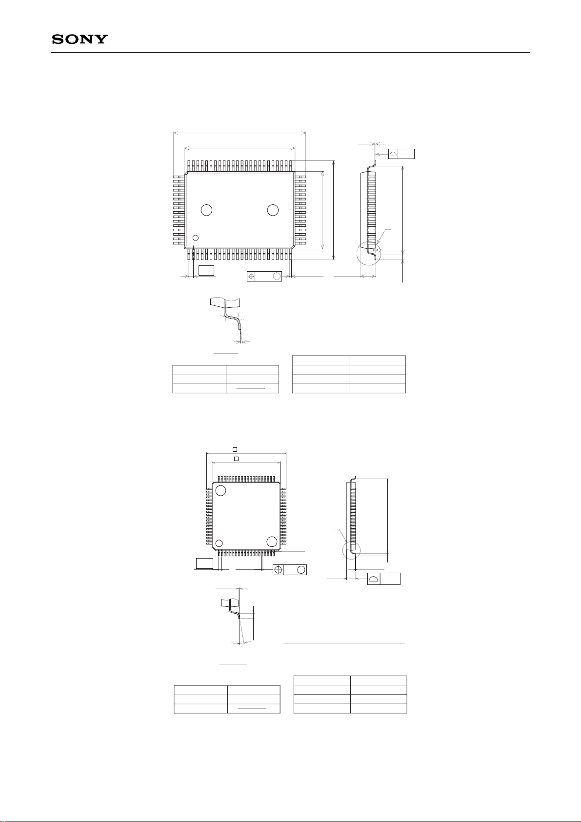
PACKAGE STRUCTURE
SONY CODE
EIAJ CODE
JEDEC CODE
QFP-80P-L01
QFP080-P-1420
PACKAGE MATERIAL
LEAD TREATMENT
LEAD MATERIAL
PACKAGE MASS
EPOXY RESIN
SOLDER PLATING
42/COPPER ALLOY
1.6g
23.9 ± 0.4
20.0 – 0.1
+ 0.4
1
80
65
64
41
40
25
24
0.8
0.35 – 0.1
+ 0.15
14.0 – 0.1
+ 0.4
17.9 ± 0.4
16.3
0.1 – 0.05
+ 0.2
2.75 – 0.15
+ 0.35
0.8 ± 0.2
0.15 – 0.05
+ 0.1
80PIN QFP (PLASTIC)
M
0.12
0.15
0° to 10°
DETAIL A
A
Package Outline Unit : mm
CXD1186CQ
CXD1186CR
CXD1186CQ/CR
—46—
SONY CODE
EIAJ CODE
JEDEC CODE
PACKAGE MATERIAL
LEAD TREATMENT
LEAD MATERIAL
PACKAGE MASS
EPOXY RESIN
SOLDER PLATING
42 ALLOY
PACKAGE STRUCTURE
14.0 ± 0.2
∗ 12.0 ± 0.1
(0.22)
60
41
40
21
20
80
61
1
0.18 – 0.03
+ 0.08
A
1.5 – 0.1
+ 0.2
0.127 – 0.02
+ 0.05
0.5 ± 0.2
(13.0)
0.1 ± 0.1
0.5 ± 0.2
0° to 10°
DETAIL A
80PIN LQFP (PLASTIC)
0.5g
LQFP-80P-L01
LQFP080-P-1212
0.1
NOTE: Dimension “∗” does not include mold protrusion.
0.13
M
0.5
 Loading...