

Page 1

—1—
E89X38F01
Sony reserves the right to change products and specifications without prior notice. This information does not convey any license by
any implication or otherwise under any patents or other right. Application circuits shown, if any, are typical examples illustrating the
operation of the devices. Sony cannot assume responsibility for any problems arising out of the use of these circuits.
Absolute Maximum Ratings (Ta=25 °C)
• Supply voltage AVDD, DVDD 7V
• Input voltage (All pins)
VIN VDD +0.5 to VSS –0.5 V
• Output current IOUT 15 mA
• Storage temperature
Tstg –55 to +150 °C
Recommended Operating Conditions
• Supply voltage AVDD, AVSS 4.75 to 5.25 V
DVDD, DVSS 4.75 to 5.25 V
• Reference input voltage
VREF 2.0 V
• Clock pulse width
Tpw1,Tpw0 11.2 ns (min) to 1.1 µs (max)
• Operating temperature
Topr –40 to +85 °C
Description
The CXD1171M is a 8-bit 40 MHz high speed D/A
converter. The adoption of a current output system
reduces power consumption to 80 mW (200 Ω load
at 2 Vp-p output).
This IC is suitable for digital TV and graphic
display applications.
Features
• Resolution 8-bit
• Max. conversion speed 40MSPS
• Non linearity error within ±0.25 LSB
• Low glitch noise
• TTL CMOS compatible input
• +5 V single power supply
• Low power consumption 80 mW
(200 Ω load at 2 Vp-p output)
Function
8-bit 40 MHz D/A converter
Structure
Silicon gate CMOS IC
8-bit 40MSPS High Speed D/A Converter
24 pin SOP (Plastic)
CXD1171M
Page 2

—2—
CXD1171M
Block Diagram and Pin Configuration
6MSB'S
CURRENT
CELLS
LATCHES
DECODER
19
20
21
22
23
24
CLOCK
GENERATOR
2
3
4
5
6
7
8
9
10
11
12
13
14
15
16
17
18
1
CURRENT CELLS
(FOR FULL SCALE)
BIAS VOLTAGE
GENERATOR
DECODER
2LSB'S
CURRENT
CELLS
(LSB) D0
D1
D2
D3
D4
D5
D6
(MSB) D7
BLK
DV
SS
VB
CLK
DV
DD
DVDD
AVDD
IO
IO
AV
DD
AVDD
VG
VREF
IREF
AV
SS
DVSS
Page 3
—3—
CXD1171M
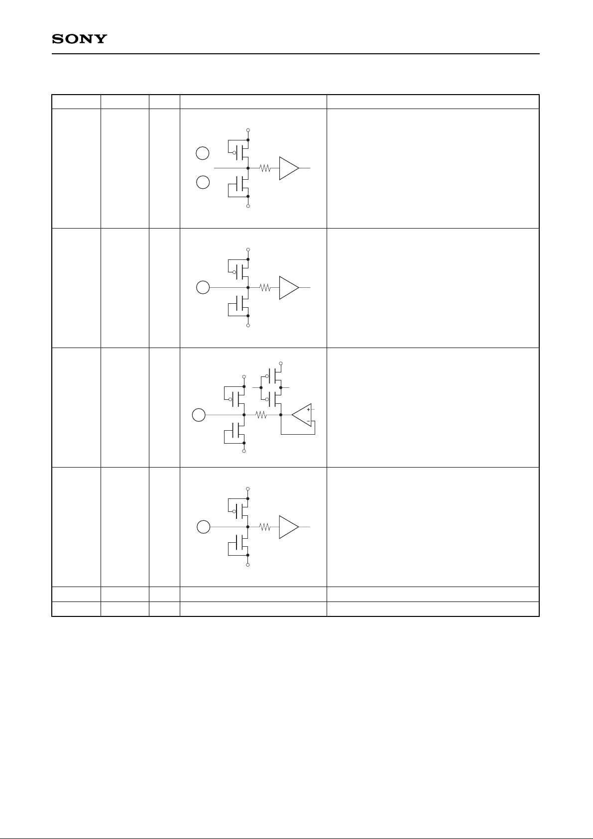
Pin Description and I/O Pins Equivalent Circuit
1 to 8
9
11
12
10, 13
14
D0 to D7
BLK
VB
CLK
DVSS
AVSS
I
I
O
I
—
—
No. Symbol I/O Equivalent circuit Description
DVDD
DVSS
to
8
1
DVDD
DVSS
9
DVDD
DVSS
DVDD
11
DVDD
DVSS
12
Digital input.
D0 (LSB) to D7 (MSB)
D0 and D1 have a pull-down resistor.
Blanking input.
This is synchronized with the clock signal.
No signal at “H” (Output 0 V).
Output condition at “L”.
Connect a capacitor of about 0.1 µF.
Clock input.
Digital ground.
Analog ground.
Page 4

—4—
CXD1171M
15
16
17
18, 19, 22
20
21
23, 24
IREF
VREF
VG
AVDD
IO
IO
DVDD
O
I
O
—
O
—
No. Symbol I/O Equivalent circuit Description
AVSS
AVSS
AVDD
AVDD
AVSS
AVDD
AVDD
15
16
17
AVDD
AVSS
AVDD
AVSS
20
21
Set full-scale output value.
Connect a capacitor of about 0.1 µF.
Analog power supply.
Current output.
Voltage output can be obtained by connecting
a resistance.
Inverted current output.
Normally connected to analog GND.
Digital power supply.
Connect a resistor “RIR” 16 times against the
output resistance value “ROUT” connected to
Pin 20 (IO).
Page 5

—5—
CXD1171M
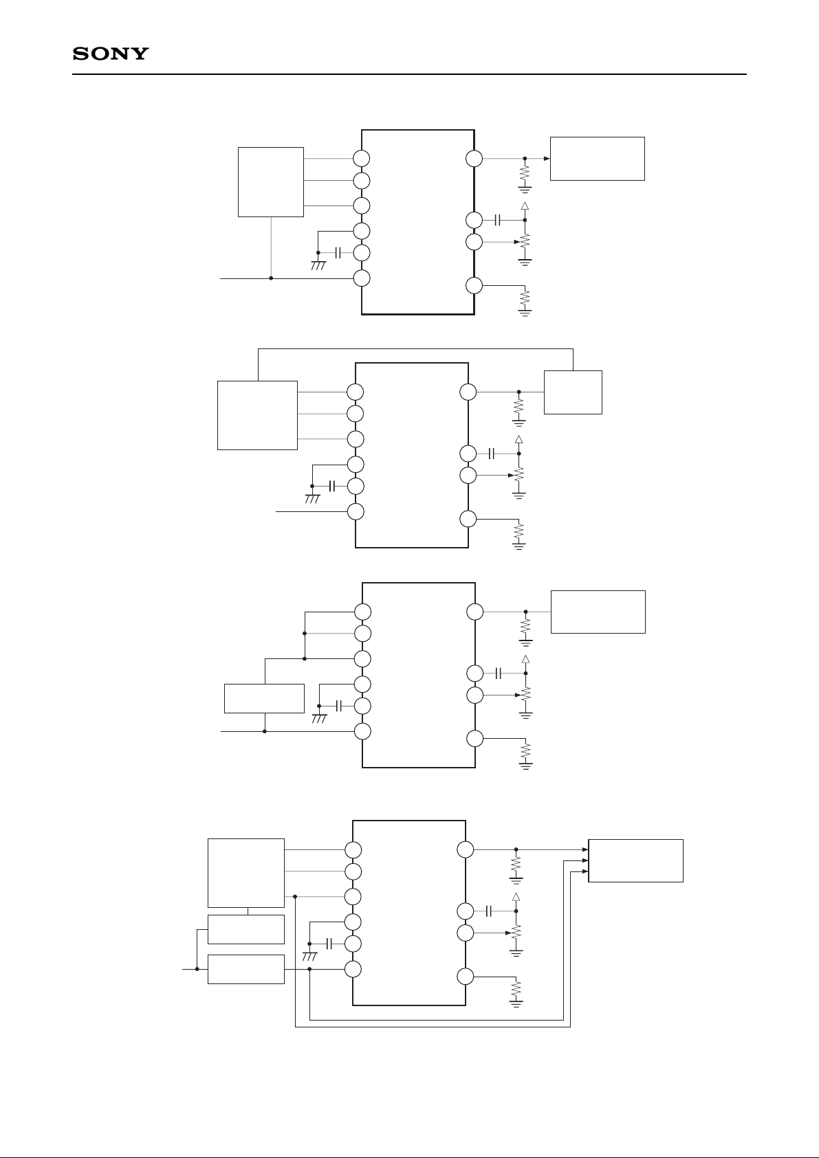
Electrical Characteristics Measurement Circuit
Analog Input Resistance
Measurement Circuit
Digital Input Current
CXD1171M
+5.25V
AVDD, DVDD
AVSS, DVSS
V
A
}
Electrical Characteristics (FCLK=40 MHz, AVDD=DVDD=5 V, ROUT=200 Ω, VREF=2.0 V, Ta=25 °C)
Item
Resolution
Conversion speed
Integral non-linearity error
Differential non-linearity error
Output full-scale voltage
Output full-scale current
Output offset voltage
Glitch energy
Supply current
Analog input resistance
Input capacitance
Digital input voltage
Digital input current
Setup time
Hold time
Propagation delay time
Symbol
n
FCLK
EL
ED
VFS
IFS
VOS
GE
IDD
RIN
CI
VIH
VIL
IIH
IIL
tS
tH
tPD
Measurement conditions
AVDD=DVDD=4.75 to 5.25 V
Ta=–40 to 85 °C
Endpoint
When D0 to D7=00000000 input
ROUT=75Ω
When 14.3 MHz color bar data input
VREF
AVDD=DVDD=4.75 to 5.25 V
Ta=–20 to +75 °C
AVDD=DVDD=4.75 to 5.25 V
D0, D1
Ta=–20 to +75 °C D2 to 7,
BLK,
CLK
ROUT=75Ω
ROUT=75Ω
Min.
0.5
–0.5
–0.25
1.9
13
1
2.4
–5
–5
5
10
Typ.
8
2.0
10
30
14.5
10
Max.
40
1.3
0.25
2.1
15
1
16
9
0.8
240
5
Unit
bit
MSPS
LSB
LSB
V
mA
mV
pV · s
mA
MΩ
pF
V
µA
ns
ns
ns
Page 6
—6—
CXD1171M
Maximum Conversion Speed Measurement Circuit
CLK
40MHZ
SQUARE
WAVE
CLK
0.1µ
200
OSCILLOSCOPE
BLK
VB
IO
VG
VREF
IREF
1k
AVss
0.1µ
3.3k
AV
DD
8
9
11
12
15
16
17
20
D7
D0 (LSB)
8bit
COUNTER
with
LATCH
•
•
•
2V
1
2
DC Characteristics Measurement Circuit
CLK
40MHZ
SQUARE
WAVE
CLK
0.1µ
200
BLK
VB
IO
VG
VREF
IREF
1k
AVss
0.1µ
3.3k
AV
DD
8
9
11
12
15
16
17
20
D7
D0 (LSB)
•
•
•
DVM
2V
CONTROLLER
2
1
Propagation Delay Time Measurement Circuit
CLK
10MHZ
SQUARE
WAVE
CLK
0.1µ
200
OSCILLOSCOPE
BLK
VB
IO
VG
VREF
IREF
1k
AVss
0.1µ
3.3k
AV
DD
8
9
11
12
15
16
17
20
D7
D0 (LSB)
•
•
•
FREQUENCY
DEMULTIPLIER
2
1
CLK
1MHZ
SQUARE
WAVE
CLK
0.1µ
75
OSCILLOSCOPE
BLK
VB
IO
VG
VREF
IREF
1k
AVss
0.1µ
1.2k
AV
DD
8
9
11
12
15
16
17
20
D7
D0 (LSB)
8bit
COUNTER
with
LATCH
•
•
•
1V
DELAY
CONTROLLER
DELAY
CONTROLLER
2
1
Setup Time
Hold Time measurement Circuit
Glitch Energy
}
Page 7
—7—
CXD1171M
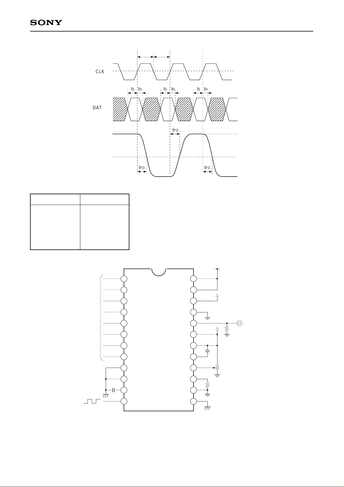
Operation
Timing Chart
tPW1 tPW0
AA
AA
tS tH tS tH tS tH
tPD
tPD tPD
CLK
DATA
D/A OUT
2V
100%
50%
0%
Application Circuit
DVDD
AVDD
200
0.1µ
2V
0.1µ
1k
3.3k
DGND
D/A OUT
AGND
19
20
21
22
23
24
13
14
15
16
17
18
8bit
DIGITAL
INPUT
3
4
5
6
7
8
9
10
11
12
(LSB)
2
1
I/O Chart (when full-scale output voltage at 2.00 V)
Input code
MSB LSB
1 1 1 1 1 1 1 1
:
1 0 0 0 0 0 0 0
:
0 0 0 0 0 0 0 0
Output voltage
2.0 V
1.0 V
0 V
Application circuits shown are typical examples illustrating the operation of the devices. Sony cannot assume responsibility for
any problems arising out of the use of these circuits or for any infringement of third party patent and other right due to same.
Page 8

—8—
CXD1171M
Notes on Operation
• How to select the output resistance
The CXD1171M is a D/A converter of the current output type. To obtain the output voltage connect the
resistance to the current output pin IO. For specifications we have:
Output full scale voltage VFS = 1.9 to 2.1 [V]
Output full scale current IFS = less than 15 [mA]
Calculate the output resistance value from the relation of VFS = IFS × ROUT. Also, 16 times resistance of the
output resistance is connected to reference current pin IREF. In some cases, however, this turns out to be a
value that does not actually exist. In such a case a value close to it can be used as a substitute. Here please
note that VFS becomes VFS = VREF × 16ROUT/RIR. ROUT is the resistance connected to IO while RIR is connected
to IREF. Increasing the resistance value can curb power consumption. On the other hand glitch energy and
data settling time will inversely increase. Set the most suitable value according to the desired application.
• Phase relation between data and clock
To obtain the expected performance as a D/A converter, it is necessary to set properly the phase relation
between data and clock applied from the exterior. Be sure to satisfy the provisions of the setup time (tS) and
hold time (tH) as stipulated in the Electrical Characteristics.
• Power supply and ground
To reduce noise effects separate analog and digital systems in the device periphery. For the power supply
pins, both digital and analog, bypass respective grounds by using a ceramic capacitor of about 0.1 µF, as
close as possible to the pin.
• Latch up
AVDD and DVDD have to be common at the PCB power supply source. This is to prevent latch up due to
voltage difference between AVDD and DVDD pins when power supply is turned ON.
• IO pin
The IO pin is the inverted current output pin described in the Pin Description. The sum of the currents output
from the IO pin and the IO pin becomes the constant value for any input data.
However, the performances such as the linearity error of the IO pin output current is not guaranteed.
Page 9
—9—
CXD1171M
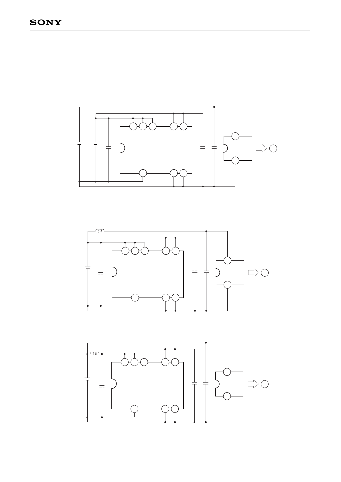
Latch Up Prevention
The CXD1171M is a CMOS IC which requires latch up precautions. Latch up is mainly generated by the lag in
the voltage rising time of AVDD (Pins 18, 19 and 22) and DVDD (Pins 23 and 24), when power supply is ON.
1. Correct usage
a. When analog and digital supplies are from different sources
b. When analog and digital supplies are from a common source
(i)
(ii)
+5V
AV
DD
+5V
AV
SS
DVSS
AVSS DVSS
AVDD DVDD
CXD1171M
DV
DD
DIGITAL IC
18 19
22
24
10
13
14
23
CC
+5V
AVSS
DVSS
AVSS DVSS
AVDD DVDD
CXD1171M
DV
DD
DIGITAL IC
18 19
22
24
10
13
14
23
C
C
+5V
AV
SS
DVSS
AVSS DVSS
AVDD DVDD
CXD1171M
DVDD
DIGITAL IC
18 19 22 24
10 1314
23
C
C
Page 10

—10—
CXD1171M
2. Example when latch up easily occurs
a. When analog and digital supplies are from different sources
b. When analog and digital supplies are from common source
(i)
(ii)
+5V
AV
DD
+5V
AV
SS
DVSS
AVSS DVSS
AVDD DVDD
CXD1171M
DV
DD
DIGITAL IC
C
18 19
22
24
10
13
14
23
C
+5V
AV
SS
DVSS
AVSS DVSS
AVDD DVDD
CXD1171M
DVDD
DIGITAL IC
AVDD
18 19
22
24
10
13
14
23
C
C
+5V
AV
SS
DVSS
AVSS DVSS
AVDD DVDD
CXD1171M
DV
DD
DIGITAL IC
AVDD
18 19
22
24
10
13
14
23
C
Page 11

—11—
CXD1171M
1.0
0
1.0
2.0
Reference voltage vs. Output full scale voltage
Reference voltage V
REF [V]
Output full scale voltage V
FS
[V]
2.0
0 255075–25
0
Output full-scale voltage V
FS
[V]
1.9
2.0
Ambient temperature vs. Output full scale voltage
Ambient temperature Ta [°C]
100
100
Output resistance vs. Glitch energy
Output resistance ROUT [Ω]
Glitch energy GE [pV · s]
200
200
AVDD=DVDD= 5.0V
VREF=2.0V
ROUT=200Ω
RIR=3.3kΩ
AVDD=DVDD=5.0V
VREF=2.0V
RIR 16ROUT
Ta=25°C
AVDD=DVDD=5.0V
ROUT=200Ω
RIR=3.3kΩ
Ta=25°C
0
≈
Page 12
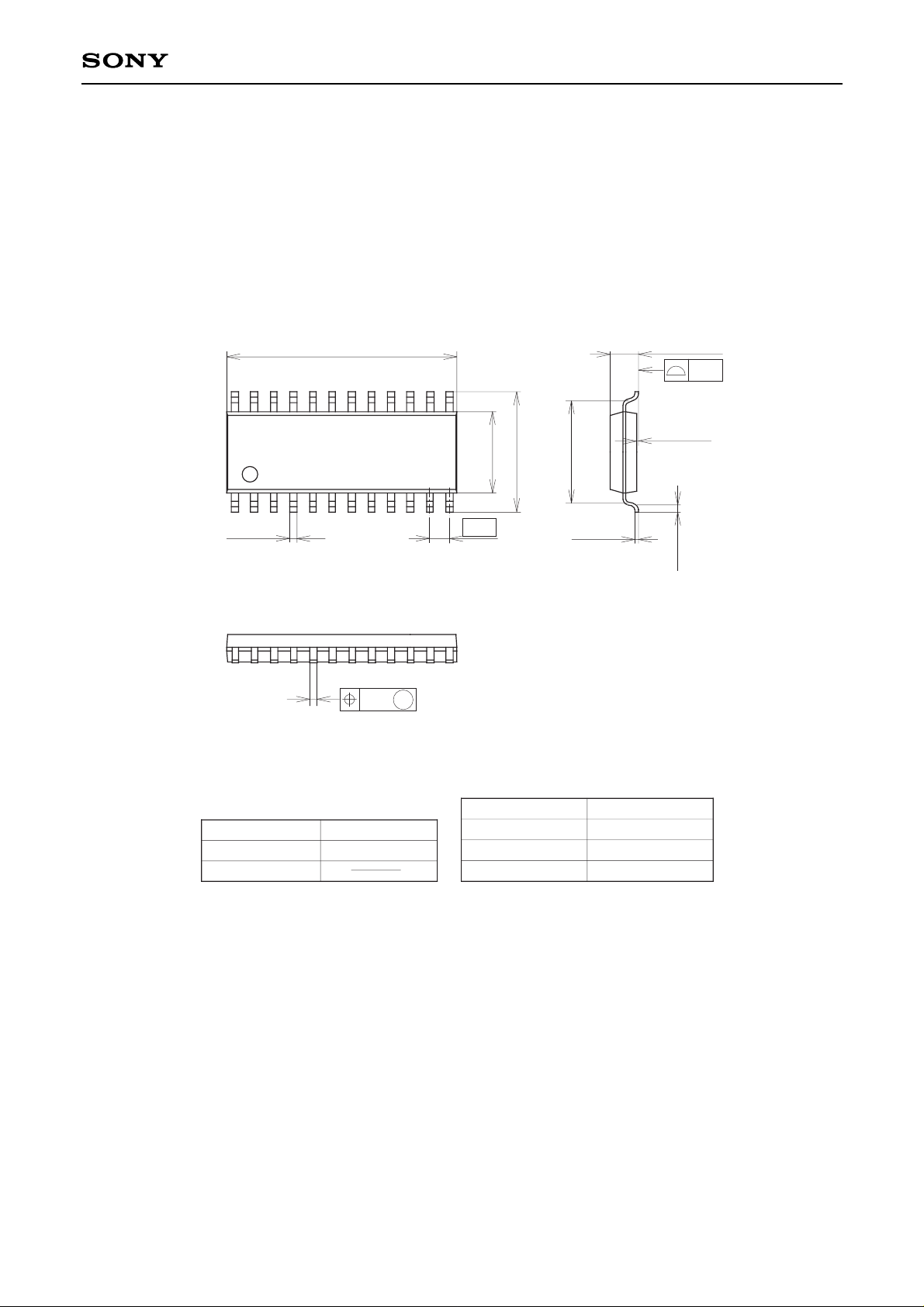
SONY CODE
EIAJ CODE
JEDEC CODE
M
PACKAGE STRUCTURE
MOLDING COMPOUND
LEAD TREATMENT
LEAD MATERIAL
PACKAGE MASS
EPOXY RESIN
SOLDER PLATING
42/COPPER ALLOY
24PIN SOP (PLASTIC)
15.0 – 0.1
+ 0.4
1
12
13
24
0.45 ± 0.1
5.3 – 0.1
+ 0.3
7.9 ± 0.4
0.2 – 0.05
+ 0.1
0.5 ± 0.2
0.1 – 0.05
+ 0.2
0.15
1.85 – 0.15
+ 0.4
6.9
0.24
SOP-24P-L01
SOP024-P-0300
0.3g
1.27
Package Outline Unit : mm
CXD1171M
—12—
 Loading...