

Page 1

– 1 –
CXB1585N
E96301-ST
Fibre Channel Repeater
Description
The CXB1585N is a repeater IC with a built-in PLL
clock recovery circuit for Fibre Channel 1.06Gbaud.
This IC incorporates a port bypass circuit and is
suitable for disk array and FC-AL HUB, etc.
Features
• Conforms to ANSI X3T11 Fibre Channel standard
• Single 3.3V power supply
• Low power consumption: 330mW (Typ.)
• Low jitter
• PLL lock detection circuit
• Port bypass circuit
• Small plastic package (24-pin SSOP)
Applications
• Fibre channel arbitrated loop 1.0625Gbaud HUB
• Disk array
Structure
Bipolar silicon monolithic IC
Pin Configuration
Sony reserves the right to change products and specifications without prior notice. This information does not convey any license by
any implication or otherwise under any patents or other right. Application circuits shown, if any, are typical examples illustrating the
operation of the devices. Sony cannot assume responsibility for any problems arising out of the use of these circuits.
24 pin SSOP (Plastic)
13
14
15
16
17
18
19
20
21
22
23
24
2
3
4
5
6
7
8
9
10
11
12
1
LPFNEG
LPFPOS
V
CCP
TDOUT
∗
TDOUT
LKDT
TEST2
SDOUT
∗
SDOUT
V
CCE
V
EEE
V
EEG
REXT
VEEP
V
EET
REFCLK
TDIN
SDIN
∗
SDIN
V
CCG
TEST1
TDIN
∗
LKREF
∗
TDSEL
∗
Page 2

– 2 –
CXB1585N
Block Diagram
SDOUT
LKDT
TDSEL
∗
LKREF
∗
TDIN
∗
TDIN
TDOUT
∗
TDOUT
LPFPOS
LPFNEG
REXT
MUX
MUX
Sig
Det
Lock
Det
÷ 20
Freq
Det
Phase
Det
DFF
SDIN
∗
SDIN
SDOUT
∗
REFCLK
53.125MH
Z
53.125MH
Z
(TTL)
(TTL)
1.063GBPS
(ECL)
1.063GBPS
(ECL)
1.063GBPS
(ECL)
1.063GBPS
(ECL)
(TTL)
(TTL)
VCO
0
1
S
0
1
S
Page 3

– 3 –
CXB1585N
Absolute Maximum Ratings (VEEE, VEET, VEEG, VEEP = 0V)
Item Unit
V
V
V
V
mA
mA
mA
°C
°C
4
5.5
VCC
2
0
20
0
70
150
–0.3
–0.5
VCC – 2
–2
–20
0
–30
–55
–65
VCC
VI_T
VI_E
VIS_E
IOH_T
IOL_T
IO_E
Ta
Tstg
Supply voltage
TTL DC input voltage
ECL DC input voltage
ECL differential input voltage
TTL output current (High level)
TTL output current (Low level)
ECL output current
Operating ambient temperature
Storage temperature
Max.Typ.Min.Symbol
Recommended Operating Conditions (VEEE, VEET, VEEG, VEEP = 0V)
Item Unit
V
°C
3.465
70
3.33.135
0
VCC
Ta
Supply voltage
Ambient temperature
Max.Typ.Min.Symbol
Page 4

– 4 –
CXB1585N
Pin Description
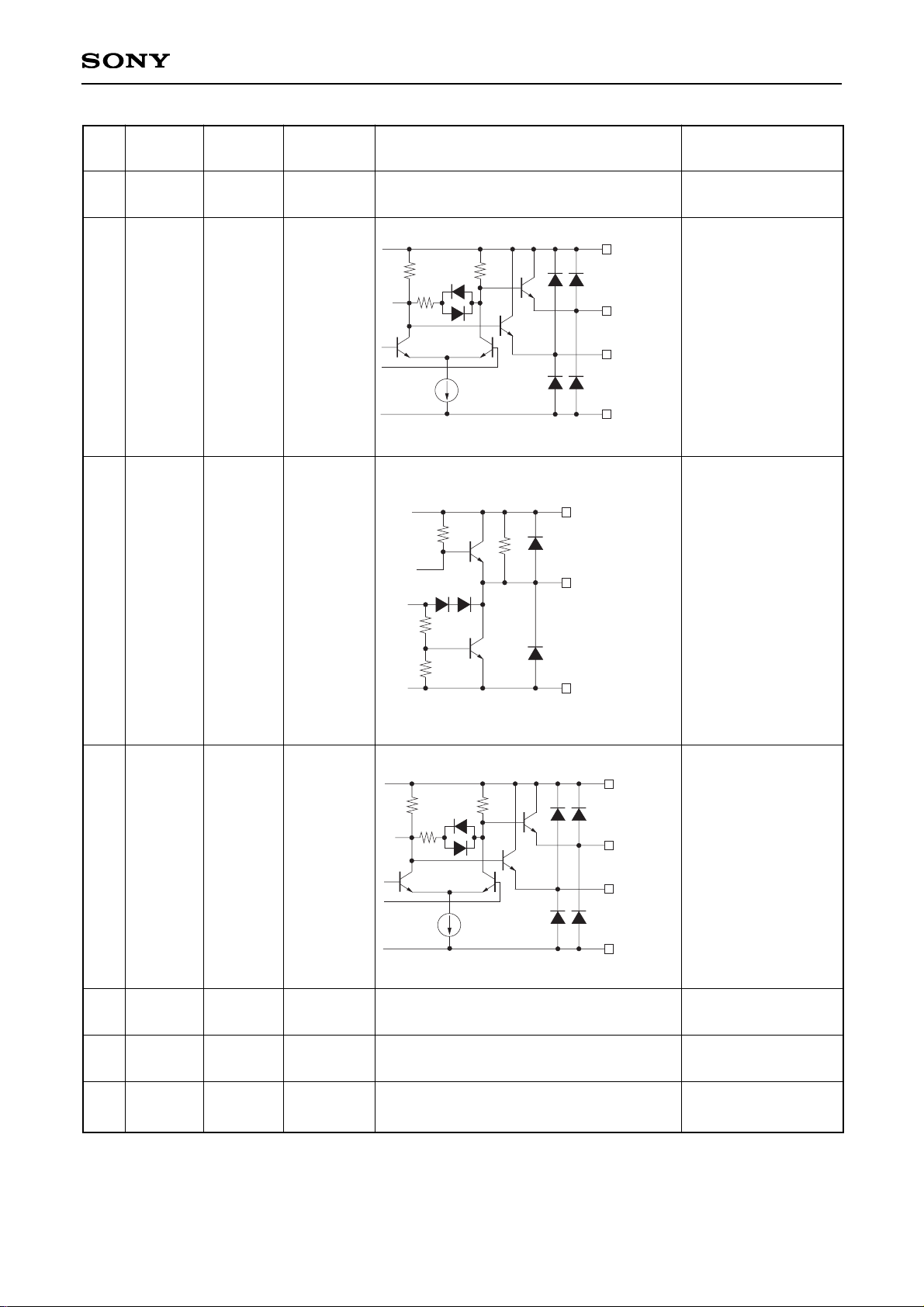
Pin
No.
Symbol Type
Typical pin
I/O voltage
Equivalent circuit Description
TEST1
TEST2
TTL
input
3.3V
1, 19
Test pin.
Connect to Vcc.
3
TDSEL
∗
TTL
input
TTL level
High; SDOUT outputs
the SDIN
retimed data.
Low; SDOUT outputs
TDIN data.
VEET
VCCG
TTL_IN
V
EEE
4, 5
SDIN
SDIN
∗
ECL
input
ECL level
Serial data input.
VCCE
VEEE
ECL_IN
ECL_IN
∗
VCCG
V
EEG
V
CCE – 1.3V
6
LKREF
∗
TTL
input
TTL level
Low; PLL takes the
frequency from
REFCLK.
VEET
VCCG
TTL_IN
V
EEE
VEET
VCCG
TTL_IN
V
EEE
2
VCCG
Power
supply
3.3V
—
Positive power supply
for internal logic gate.
Page 5

– 5 –
CXB1585N
9
REFCLK
TTL
input
TTL level
Reference clock input.
This pin is used for
the PLL to take the
frequency.
Input 53.125MHz to
this pin.
VEET
VCCG
TTL_IN
V
EET
10
VEET
Power
supply
0V
Negative power supply
for REFCLK input.
11
VEEP
Power
supply
0V
Negative power supply
for internal PLL.
12
REXT
External
parts
connection
pin
—
Connects the resistor
which determines the
VCO center
frequency.
4.7kΩ resistor should
be connected
between this pin and
VEEP.
VCCP
VEEP
REXT
13,
14
LPFNEG
LPFPOS
External
parts
connection
pin
—
Connects the
external loop filter.
VCCP
VEEP
LPF_A
LPF_B
7, 8
TDIN
TDIN
∗
ECL
input
ECL level
Serial data input.
VCCE
VEEE
ECL_IN
ECL_IN
∗
VCCG
V
EEG
V
CCE – 1.3V
Pin
No.
Symbol Type
Typical pin
I/O voltage
Equivalent circuit Description
Page 6
– 6 –
CXB1585N
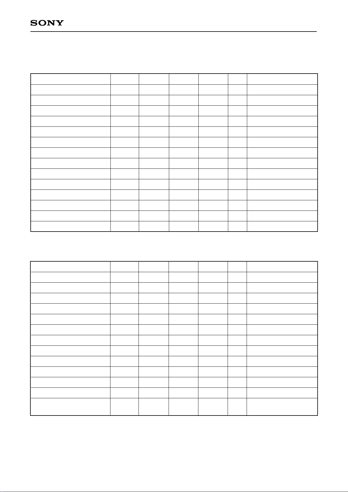
18
LKDT
TTL
output
TTL level
PLL clock detection
signal output.Outputs
high level when PLL is
locked to the serial
data;Outputs low level
when LKREF is in the
low level or the serial
data has no signal.
The LKDT output may
sporadically go high
when the PLL starts to
lock to the serial data.
VEEE
VCCE
TTL_OUT
20,
21
SDOUT
∗
SDOUT
ECL
output
ECL level
Outputs the serial
data selected by
TDSEL∗.
VCCE
VEEE
ECL_OUT
ECL_OUT
∗
22
VCCE
Power
supply
—
Positive power supply
for input/output.
23
VEEE
Power
supply
—
Negative power supply
for input/output.
24
VEEG
Power
supply
—
Negative power supply
for internal logic gate.
16,
17
TDOUT
∗
TDOUT
ECL
output
ECL level
Outputs the data input
from TDIN via a
buffer.
VCCE
VEEE
ECL_OUT
ECL_OUT
∗
15
VCCP
Power
supply
3.3V
Positive power supply
for PLL.
Pin
No.
Symbol Type
Typical pin
I/O voltage
Equivalent circuit Description
Page 7
– 7 –
CXB1585N
AC Characteristics (under the recommended operating conditions)
Item
REFCLK rise time
REFCLK fall time
TTL output rise time
TTL output fall time
ECL output rise time
ECL output fall time
SDIN data rate
REFCKL cycle tolerance
Jitter tolerance
Deterministic jitter
Random jitter
Bit sync time
Frequency take-in time
Tir_RC
Tif_RC
Tor_T
Tof_T
Tor_E
Tof_E
SDIN
Ttol_RC
JT
Dj
RJ
Tbs
Tfa
1000
–100
1062.5
0
0.02
0.18
4.8
4.8
3.5
3.5
400
400
1100
100
0.7
0.07
0.23
2500
500
ns
ns
ns
ns
ps
ps
Mbaud
ppm
Ul
Ul
Ul
bit
µs
0.8 to 2.0V
2.0 to 0.8V
0.8 to 2.0V, CL = 10pF
2.0 to 0.8V, CL = 10pF
20 to 80%, CL ≤ 2pF
20 to 80%, CL ≤ 2pF
Refer to the SDIN cycle
±K28.5 serial data
Serial data
FC Idle Pattern
Loop Damping Capacitor
C1 = 0.01µF
Symbol Min. Typ. Max. Unit Conditions
VIH_T
VIL_T
IIH_T
IIL_T
VOH_T
VOL_T
VIH_E
VIL_E
VIS_E
VOH_E
VOL_E
VOS_E
ICC
PD
2
0
–400
2.2
VCC – 1.17
VCC – 1.81
200
VCC – 1.05
VCC – 1.81
650
Electrical Characteristics
DC Characteristics (under the recommended operating conditions)
Item
TTL high level input voltage
TTL low level input voltage
TTL high level input current
TTL low level input current
TTL high level output voltage
TTL low level output voltage
ECL high level input voltage
ECL low level input voltage
ECL differential input voltage
ECL high level output voltage
ECL low level output voltage
ECL output amplitude
Current consumption
Power consumption
101
333
5.5
0.8
20
0.5
VCC – 0.88
VCC – 1.48
1000
VCC – 0.81
VCC – 1.55
127
438
V
V
µA
µA
V
V
V
V
mV
V
V
mV
mA
mW
VIH = VCC
VIL = 0
IOH = –0.4mA
IOL = 2mA
AC coupling input
50Ω terminated to Vcc – 2V
50Ω terminated to Vcc – 2V
50Ω terminated to Vcc – 2V
Output pins open
Output pins open
Symbol Min. Typ. Max. Unit Conditions
Page 8
– 8 –
CXB1585N
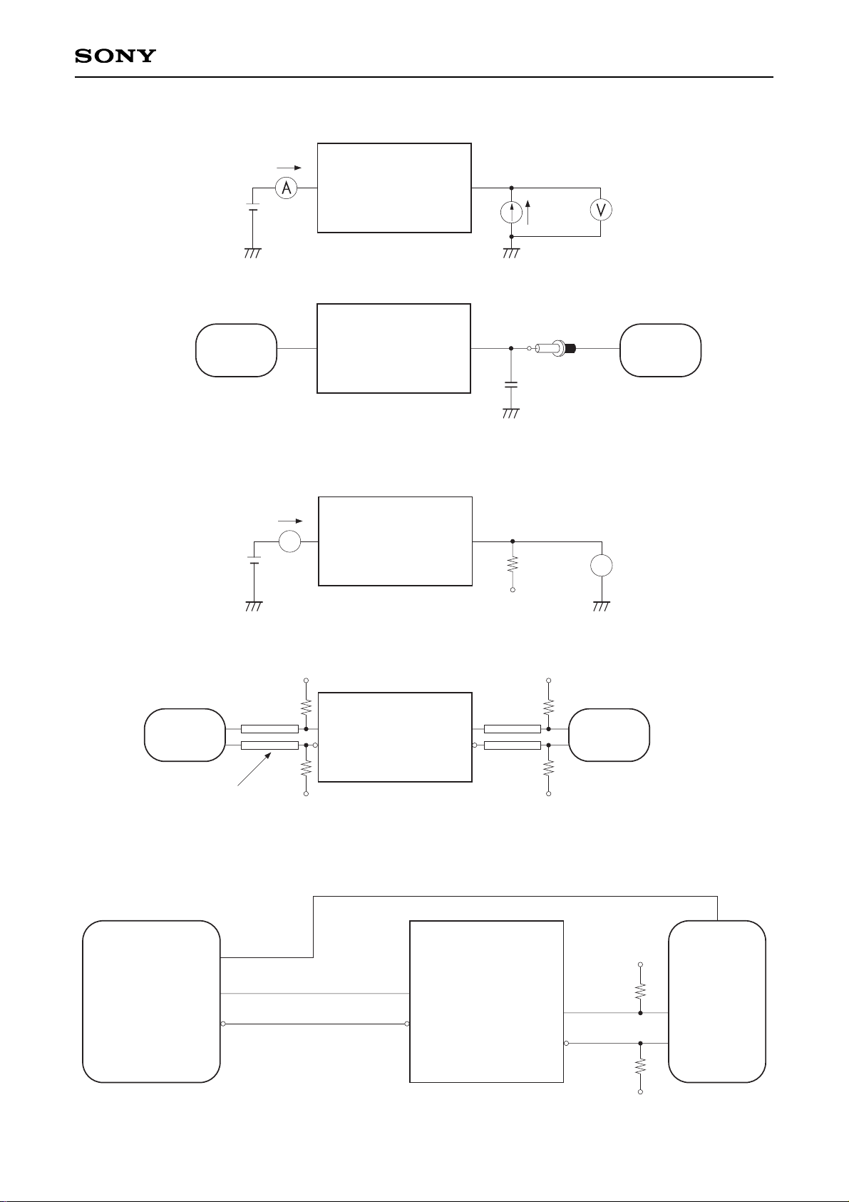
Electrical Characteristics Measurement Circuit (See “Fig. 3 Power Supply Circuit” regarding the power supply.)
TTL_IN TTL_OUT
Measurement device
Io_T
I
I_T
Vo_T
V
I_T
TTL_IN TTL_OUT
Pulse generator
Measurement
device
Oscilloscope
CL = 10pF (including the probe capacitance)
Probe
CL
(a) TTL I/O DC characteristics measurement circuit
(b) TTL I/O AC characteristics measurement circuit
ECL_IN ECL_OUT
Measurement device
50Ω
I
I_E
V
O_E
V
I_TE
VCCE – 2V
V
A
(c) ECL I/O DC characteristics measurement circuit
ECL_IN ECL_OUT
Measurement device
Pulse
generator
Oscilloscope
50Ω
VCCE – 2V
VCCE – 2V
50Ω
50Ω
VCCE – 2V
VCCE – 2V
50Ω
ECL_IN
∗
ECL_OUT
∗
CL ≤ 2pF
(input capacitance of the measurement
equipment and floating capacitance)
50Ω Transmission Line
(d) ECL I/O AC characteristics measurement circuit
SDIN
SOUT
Measurement device
Pulse generator
50Ω
VCCE – 2V
50Ω
SDIN
∗
SOUT
∗
1.0625GBPS
Oscilloscope
Triger
26.5625MHz
1.0625GBPS
V
CCE – 2V
(e) Jitter characteristics measurement circuit
Page 9

– 9 –
CXB1585N
Notes on Operation
1. Clock synthesizer (PLL)
The CXB1585N has a PLL-based clock recovery circuit for recovering the clock from the serial data. This clock
recovery circuit requires an external loop filter and an external resistor which determines the VCO center
frequency. The external part circuit and recommended constant values are shown in the figure below. The
parasitic capacitance attached to the IC pins (Pins 12, 13 and 14) which are used to connect external parts
should be kept as small as possible in order to obtain the good PLL characteristics. In addition, capacitor C1
should have a small temperature coefficient to reduce the temperature dependence of the VCO oscillation
frequency.
13
14
V
EEP
REXT
LPFPOS
LPFNEG
CXB1585N
11
12
C1
R1: 4.7kΩ
C1: 0.01µF
R1
Fig. 1. External Part Circuit and Recommended Constants
Page 10

– 10 –
CXB1585N
2. ECL input circuit
The ECL differential input pins are biased to VBB (VCC – 1.3V) via an 18kΩ resistor in the IC. See the figures
below for ECL differential input methods.
18kΩ
18kΩ
VBB (VCC – 1.3V)
VCC = 3.3V, VEE = GND
160Ω 160Ω
VCC = 3.3V, VEE = GND
ECL differential input buffer3.3V ECL output buffer
(a) ECL differential signal from 3.3V ECL output buffer
18kΩ
18kΩ
V
BB (VCC – 1.3V)
V
CC = 3.3V, VEE = GND
330Ω 330Ω
VCC = GND, VEE = –4.5V
ECL differential input bufferECL100K output buffer
VEE
330pF
330pF
220kΩ
V
CC
(b) ECL differential signal from ECL 100K output buffer
18kΩ
18kΩ
V
BB (VCC – 1.3V)
V
CC = 3.3V, VEE = GND
50Ω 50Ω
ECL differential input buffer
50Ω
TRANS.
LINE
330pF
330pF
VTT (VCC – 2V)
220kΩ
V
CC
(c) ECL differential signal from 50Ω transmission line
18kΩ
18kΩ
V
BB (VCC – 1.3V)
V
CC = 3.3V, VEE = GND
50Ω
ECL differential input buffer
50Ω
TRANS.
LINE
330pF
330pF
VTT (VCC – 2V)
220kΩ
VCC
(d) ECL single signal from 50Ω transmission line
Fig. 2. ECL Input Circuits
Page 11
– 11 –
CXB1585N
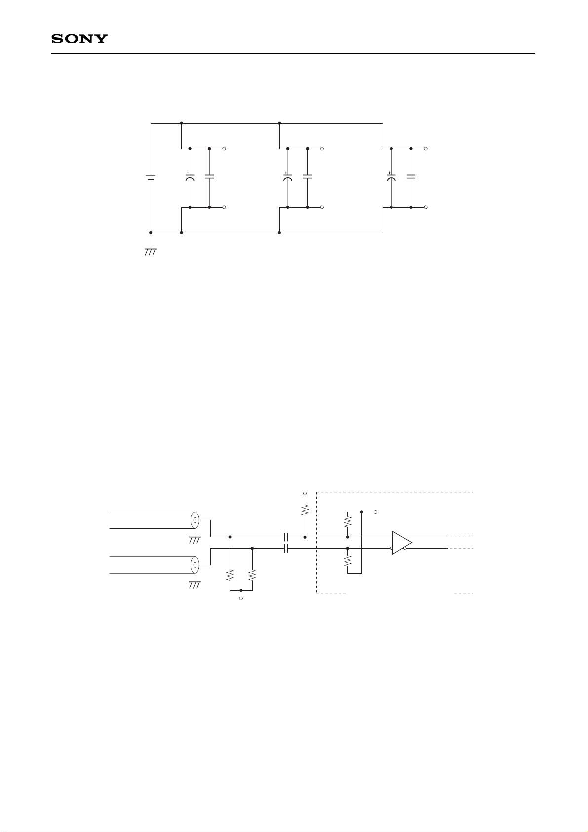
3. Power supply
VCCT
V
EET
0.1µF
22µF
3.3V
VCCG
V
EEG
0.1µF
22µF
VCCP
V
EEP
0.1µF
22µF
Fig. 3. Power Supply Circuit
4. SDIN, SDIN∗inputs
Normally, the VCO performs frequency comparison with the SDIN and SDIN∗serial data. When there is no
input to SDIN and SDIN∗, frequency comparison is executed with REFCLK. However, the frequency may not
be compared to REFCLK if the noise and others are detected as a signal for no signal state because the both
phases of the ECL differential inputs are internally biased to VBB shown below. As countermeasure to this,
connect either of the differential inputs to VCC via a resistor to generate the voltage difference for the both
phases.
ECL differential signal from 50Ω transmission line
Fig. 4. SDIN and SDIN∗Input Example
18kΩ
18kΩ
V
BB (VCC – 1.3V)
50Ω 50Ω
ECL differential input buffer
50Ω
TRANS.
LINE
330pF
330pF
VTT (VCC – 2V)
220kΩ
V
CC
Page 12
– 12 –
CXB1585N
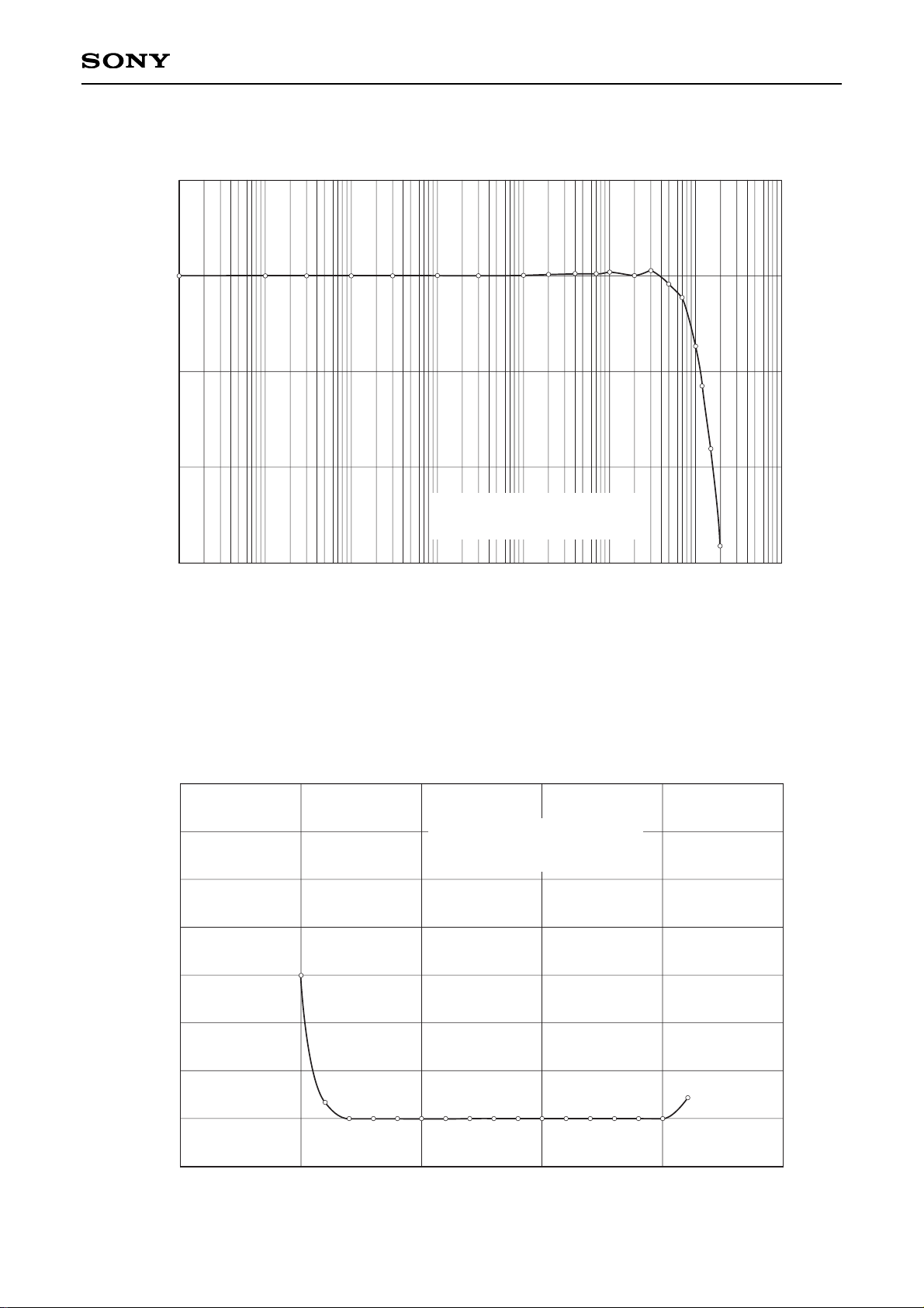
Example of Representative Characteristics
Modulation Frequency [Hz]
10
1
10
8
10
2
10
3
10
4
10
5
10
6
10
7
Jitter Transfer [dB]
–15
–10
–5
0
5
Jitter Transfer
Bit Synchronization Time
REFCLK [MHZ]
51.5 54
0
Bit Synchronization Time [ns]
4000
53.552 52.5 53
3500
3000
2500
2000
1500
1000
500
C1 = 0.01µF, R1 = 4.7kΩ, Ta = 27°C
Pattern: Fibre Channel ldle Pattern
(Transition Density = 80%)
C1 = 0.01µF, R1 = 4.7kΩ, Ta = 27°C
Pattern: Fibre Channel ldle Pattern
(Transition Density = 80%)
Page 13

– 13 –
CXB1585N
Eye pattern (Retimed data 1.0625Gbps)
[200ps/div]
[200mV/div]
Example of Random jitter measurement (Retimed data 1.0625Gbps)
[50ps/div]
[100mV/div]
C1 = 0.01µF, R1 = 4.7kΩ, Ta = 27°C
SDIN: Fibre Channel ldle Pattern
(Transition Density = 80%)
RJ = 9.6ps (RMS)
C1 = 0.01µF, R1 = 4.7kΩ, Ta = 27°C
SDIN: Fibre Channel ldle Pattern
(Transition Density = 80%)
Page 14
– 14 –
CXB1585N
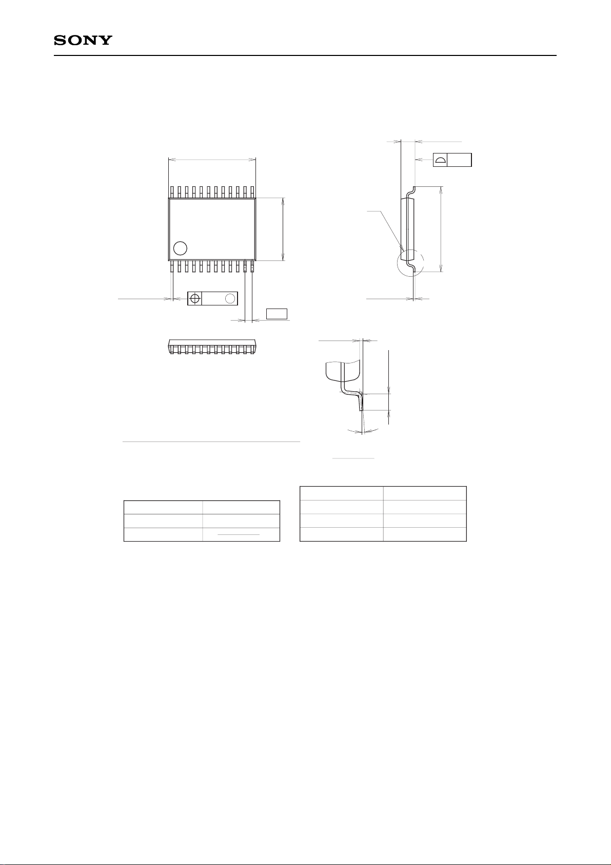
Package Outline Unit: mm
SONY CODE
EIAJ CODE
JEDEC CODE
SSOP-24P-L01
SSOP024-P-0056
PACKAGE MATERIAL
LEAD TREATMENT
LEAD MATERIAL
PACKAGE WEIGHT
EPOXY RESIN
SOLDER/PALLADIUM
42/COPPER ALLOY
PACKAGE STRUCTURE
PLATING
0.1g
24PIN SSOP(PLASTIC)
∗5.6 ± 0.1
24
∗7.8 ± 0.1
13
0.65
12
1
0.22 – 0.05
+ 0.1
0.15 – 0.02
+ 0.05
7.6 ± 0.2
0.1
1.25 – 0.1
+ 0.2
A
0.1 ± 0.1
0° to 10°
0.5 ± 0.2
DETAIL
A
NOTE: “∗” Dimensions do not include mold protrusion.
0.13
M
 Loading...