

Page 1

266Mbaud Fibre Channel Transceiver IC
For the availability of this product, please contact the sales office.
Description
The CXB1583Q is a transceiver IC with the built-in
PLLs into a single chip.
For receiver, the 265.625Mbaud serial data is
received and it is output as a 10-bit parallel data; for
transmitter, the 265.625Mbaud 10-bit parallel data is
received and it is output as a serial data after
conversion.
Features
• Transmitter/receiver into a single chip
• Conforms to ANSI X3T11 fibre channel standard
• PLL for a clock synthesizing and for clock recovery
• Single 3.3V power supply
• Low power consumption: 860mW (Typ.)
• 80-pin plastic package
• Comma signal detector
• Test pattern (±K28.5) generation circuit
• Loop-back circuit
• Supports data rage of 200Mbaud
Applications
265.625Mbaud fibre channel
Structure
Bipolar silicon monolithic IC
CXB1583Q
80 pin QFP (Plastic)
Pin Configuration
SDOUT
SDOUT
TXSIN
TXSIN
ECKENB
ALTENB
TPGEN
TXSER
REFCLK
V
CCE
EEE
V
LOL
EEG
V
CCG
V
V
EEG
CCG
V
LPBK
EET
V
CCG
V
EEG
V
∗
ECK
49
ECK
48
∗
TXSOUT
TXSOUT
47
46
∗
E
E
CC
EE
SDIN
V
V
43
45
44
SDIN
42
G
G
CC
EE
V
V
41
40
MS1
MS0
39
CDETENB
38
37
CCT
V
∗
36
POR
35
TXLKDT
RXLKDT
34
EET
V
33
32
PCLKOUT0
PCLKOUT1
31
EEG
V
30
CCG
V
29
CDET
28
PDO9
27
PDO8
26
EET
V
25
PDO7
24
CCT
V
23
VCCG
22
EEG
V
21
∗
LPFB
52
LPFA
51
P
CC
V
50
P1
P2
EE
EE
REXT
TJMON
LPFC
LPFD
LCKREF
60
61
∗
62
63
64
65
∗
66
67
68
69
∗
70
71
72
73
∗
74
∗
75
76
77
78
79
80
59
58
57
56
55
V
V
53
54
1
PDI0
2
PDI1
3
PDI2
4
PDI3
5
PDI4
6
PDI5
7
8
PDI6
9
PDI7
10
PDI8
11
PDI9
12
PDO0
13
PDO1
14
15
16
T
T
EE
CC
V
V
PDO3
PDO2
17
18
PDO4
19
20
T
EE
V
PDO6
PDO5
Sony reserves the right to change products and specifications without prior notice. This information does not convey any license by
any implication or otherwise under any patents or other right. Application circuits shown, if any, are typical examples illustrating the
operation of the devices. Sony cannot assume responsibility for any problems arising out of the use of these circuits.
– 1 –
E96501-ST
Page 2

CXB1583Q
Absolute Maximum Ratings (VEEE, VEET, VEEG, VEEP = 0V)
Item Unit
Power supply
TTL DC input voltage
ECL DC input voltage
ECL differential input voltage
TTL output current (high level)
TTL output current (low level)
ECL output current
Operating ambient temperature
Storage temperature
VCC
VI_T
VI_E
VIS_E
IOH_T
IOL_T
IO_E
Ta
Tstg
–0.3
–0.5
VCC – 2
–2
–20
0
–30
–55
–65
Max.Typ.Min.Symbol
5.5
VCC
20
70
150
4
V
V
V
2
0
V
mA
mA
0
mA
°C
°C
Recommended Operating Conditions (VEEE, VEET, VEEG, VEEP = 0V)
Supply voltage
Ambient temperature
Item Unit
VCC
Ta
0
3.33.135
Max.Typ.Min.Symbol
3.465
70
V
°C
– 2 –
Page 3

Block Diagram
CXB1583Q
PDI (0 to 9)
ALTENB
∗
REFCLK
10
26.6Mbps
REFCLK
(26.6MHz)
DQ
10
K28.5
Gen.
TX_PLL
∗
TPGEN
1
0
TXCLK (26.6MHz)
TXLOAD (266MHz)
P/S
TXSER
SoutPin
TXSIN
∗
TXSIN
0
1
TXSOUT
TXSOUT
SDOUT
SDOUT
TXLKDT
∗
∗
EEP
V
PDO (0 to 9)
PCLKOUT0
PCLKOUT1
CDET
LPFA
LPFB
REXT
26.6Mbps
10
S/P
CDETENB
RTDATA
RXCLK (266MHz)
RPCLK (26.6M)
RX_PLL
LPFC
LPFD
LPBK
SDIN
1
0
∗
SDIN
LOL
RXLKDT
∗
LCKREF
– 3 –
Page 4

Pin Description
CXB1583Q
Pin
No.
Symbol Type
1 t o 1 0 PDI0 to 9
11, 12,
14, 16,
17, 19,
PDO0 to 9
20, 24,
26, 27
TTL
input
TTL
output
Typical pin
I/O voltage
TTL level
TTL level
VCCG
TTL-IN
VEET
Equivalent circuit Description
Parallel data input.
VEEG
VCCT
TTL-OUT
Parallel data output.
13, 18,
25, 33,78VEET
15, 23,
37
VCCT
21, 30,
42, 68,
VEEG
71, 80
22, 29,
41, 69,
VCCG
72, 79
28 CDET
Power
supply
Power
supply
Power
supply
Power
supply
TTL
output
0V —
3.3V —
0V —
3.3V —
TTL level
VEET
VCCT
TTL-OUT
VEET
Negative power
supply for TTL
input/output.
Positive power supply
for TTL output.
Negative power
supply for internal
logic gate.
Positive power supply
for internal logic gate.
Byte synchronization
output.
Outputs high level
when +Comma
(0011111) or
–Comma (1100000)
is detected to the
serial data.
– 4 –
Page 5

CXB1583Q
Pin
No.
32
31
Symbol Type
PCLKOUT0
PCLKOUT1
TTL
output
TTL
output
Typical pin
I/O voltage
TTL level
TTL level
Equivalent circuit Description
VCCT
Receive byte clock 0
TTL-OUT
output.
This clock is used to
take the parallel data
(PDO0 to 9) at the
next-stage system.
VEET
VCCT
Receive byte clock 1
TTL-OUT
output.
PCLKOUT0 inverted
clock.
34 RXLKDT
TXLKDT
35
TTL
output
TTL
output
TTL level
TTL level
VEET
VCCT
TTL-OUT
VEET
VCCT
TTL-OUT
VEET
RX_PLL lock
detection signal
output.
Outputs high level
when the PLL is
locked to the serial
data or the serial data
has no signal; Outputs
low level when the
PLL is not locked.
RXLKDT output may
sporadically go high
when the PLL starts
to lock to the serial
data.
TX_PLL lock
detection signal output.
Outputs high level
when the PLL is
locked to REFCLK
and operating
normally; Outputs low
level when the PLL is
not operating
normally.
– 5 –
Page 6

CXB1583Q
Pin
No.
36
Symbol Type
∗
POR
38 CDETENB
TTL
output
TTL
input
Typical pin
I/O voltage
TTL level
TTL level
VCCG
TTL-IN
VEET
Equivalent circuit Description
VCCT
Power-on reset signal
output.
TTL-OUT
Outputs high level
after the power is
turned on and low
level is held for
approximately 100ns.
VEET
Byte synchronization
enable signal input.
When high level is
input, +Comma
(0011111) or –Comma
(1100000) is detected
and the parallel data
is synchronized with
this byte. (See the
Timing Chart.)
When low level is input,
VEEG
byte synchronization
is not performed.
39,
40
43,
44
MS0, MS1
SDIN
∗
SDIN
TTL
input
ECL
input
(differential)
3.3 V or TTL
high level
ECL level
VCCG
TTL-IN
VEET
VCCE
ECL-IN
ECL-IN
VEEE
Test pin.
Connect to Vcc.
VEEG
VCCG
VCCE – 1.3V
∗
VEEG
Serial data input.
45,
63
46,
64
VCCE
VEEE
Power
supply
Power
supply
3.3V
0V
– 6 –
—
—
Positive power supply
for ECL input/output.
Negative power
supply for ECL
input/output.
Page 7

CXB1583Q
Pin
No.
47,
48
49,
50
Symbol Type
ECL
TXSOUT
TXSOUT
∗
output
(differ-
ential)
ECL
ECK
ECK
∗
output
(differ-
ential)
Typical pin
I/O voltage
ECL level
One is left
open; another
is connected
to Vcc via
47kΩ.
VCCE
ECL-IN
ECL-IN
Equivalent circuit Description
VCCE
Parallel/serial
ECL-OUT
conversion output.
This output is
∗
ECL-OUT
enabled when
TXSER is high.
VEEE
VCCG
Test pin.
VCCE – 1.3V
∗
Connect either of
these pins to Vcc via
a 47kΩ resistor.
51 VCCP
52,53LPFA
LPFB
54,55VEEP1
VEEP2
56 REXT
Power
supply
Ex-
ternal
part
con-
nection
Power
supply
External
part
connection
3.3V
—
0V
—
VEEE
VCCP
LPF_C
LPF_D
VEEP2
—
—
VCCP
REXT
VEEG
Positive power supply
for internal PLL.
RX_PLL external loop
filter connection.
(See Fig. 1 of the
Notes on Operation.)
VEEP1
Negative power supply
for internal PLL.
Connects the resistor
which determines the
VCO center frequency.
(See Fig. 1 of the
Notes on Operation.)
– 7 –
VEEP2
Page 8
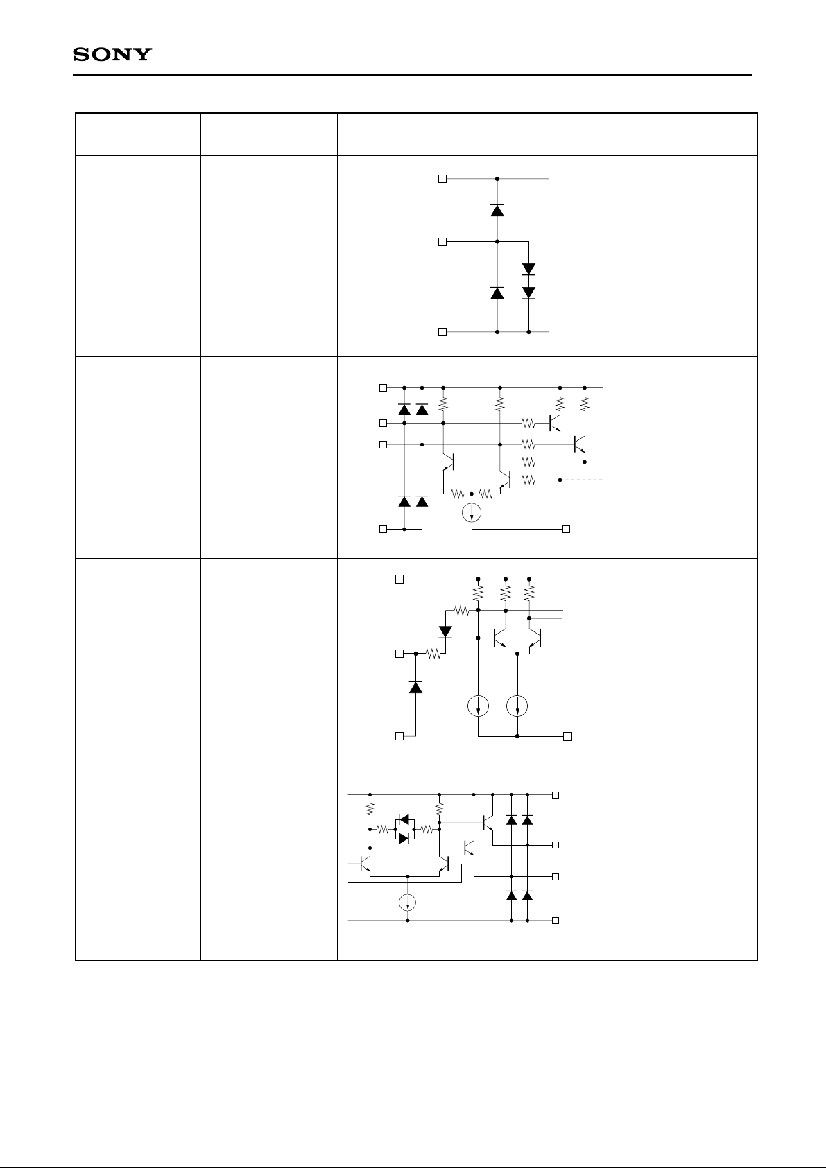
CXB1583Q
Pin
No.
Symbol Type
57 TJMON
58,59LPFC
LPFD
Test
pin
External
part
connection
Typical pin
I/O voltage
0V
—
VCCP
LPF_C
LPF_D
Equivalent circuit Description
VCCP
TJMON
Junction temperature
measurement.
VEEE2
TX_PLL external loop
filter connection.
(See Fig. 1 of the
Notes on Operation.)
60
61,
62
LCKREF
SDOUT
SDOUT
∗
∗
TTL
input
ECL
output
(differential)
TTL level
ECL level
VEEP2
VCCG
TTL-IN
VEET
VEEP1
VEEG
VCCE
ECL-OUT
ECL-OUT
VEEE
Lock-to-reference
signal input.
When this pin is set
to low level, RX_PLL
is forcibly locked to
REFCLK.
Serial data output for
transmission.
The serial data order
∗
is PDI0 → PDI9.
– 8 –
Page 9
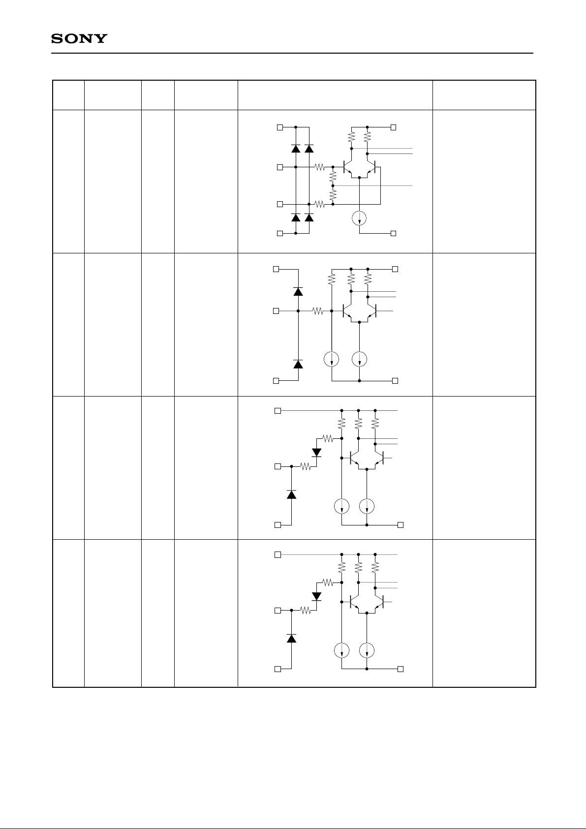
CXB1583Q
Pin
No.
65,
66
Symbol Type
TXSIN
TXSIN
67 LOL
Typical pin
I/O voltage
VCCE
ECL
input
∗
(differ-
ECL level
ential)
ECL
input
(single
Open or ECL
level
ECL-IN
ECL-IN
VEEE
VCCE
ECL-IN
phase)
Equivalent circuit Description
VCCG
Serial ECL data input.
VCCE – 1.3V
∗
VEEG
VCCG
When TXSER is high,
this input signal is
output from SDOUT.
Lost-of-light signal
VCCE – 1.3V
input.
Low level when this
pin is left open.
70
73
ECKENB
LPBK
VEEE
VCCG
TTL
∗
input
3.3V or TTL
high level
TTL-IN
VEET
VCCG
VEEG
Test pin.
VEEG
Loop-back enable.
If LPBK is set to high,
the signal output from
SDOUT when LPBK
is low is transmitted to
TTL
input
TTL level
TTL-IN
the RX input with the
internal connection.
In this time, SDOUT/
SDOUT∗are fixed to
low/high respectively
VEET
VEEG
and SDIN/SDIN∗are
both disabled.
– 9 –
Page 10

CXB1583Q
Pin
No.
74
75
Symbol Type
TTL
ALTENB
TPGEN
∗
input
TTL
∗
input
Typical pin
I/O voltage
TTL level
TTL level
VCCG
TTL-IN
VEET
VCCG
TTL-IN
VEET
Equivalent circuit Description
Alternate disparity test
pattern generation
enable.
When ALTENB∗is set
to low with TPGEN
low, K28.5 (+K28.5,
–K28.5) is generated
for the data stream
output. When this pin
is high, +K28.5 is
VEEG
generated.
Test pattern
generation enable.
When this pin is low,
+K28.5 (ALTENB∗:
high) or ±K28.5
(ALTENB∗: low) is
generated for the
data stream output.
VEEG
∗
76 TXSER
77 REFCLK
TTL
input
TTL
input
TTL level
TTL level
VCCG
TTL-IN
VEET
VCCG
TTL-IN
VEET
VEEG
VEEG
Transmit serial data
selector.
When this pin is high,
the serial data input
from TXSIN is output
from SDOUT and the
serialized PDI0 to 9
signals are output
from TXSOUT.
Transmit byte clock.
This clock is used to
take the PDI0 to 9
signals in the TXPLL.
The RXPLL takes the
frequency from
REFCLK when
LCKREF∗is low.
REFCLK is necessary
after LCKREF∗is set
to high and the
RXPLL is locked to
the serial data.
– 10 –
Page 11

CXB1583Q Functions
1. Data map to the 8b/10b alphabet notation
PDI0 is the start bit.
PDI, PDO 0 1 2 3 4 5 6 7 8 9
CXB1583Q
8b/10b alphabet notation
abcde
i
fghj
2. COMMA DETECT
When CDETENB is high and the SDIN input data row includes K28.5, PDO0 to 9 are synchronized with K28.5
and output. Byte synchronization is also performed to ±Comma.
Serial Data
+K28.5
Comma (positive)
Comma (negative)
–K28.5
PDO0
a
0
0
1
1
b
0
0
1
1
c
1
1
0
0
d
1
1
0
0
e
1
1
0
0
i
1
1
0
0
f
1
1
0
0
g
0
X
X
1
PDO9
h
1
X
X
0
j
0
X
X
1
3. TXSER, LPBK operation modes
Low
TXSER
Input
Low
LPBK
TXSOUT
Disabled/Static
Output
SDOUT
Serialized PDI
PDO0 to 9
SDIN
Low
High
High
High
Low
High
4. LCKREF∗operation modes
LCKREF input level
High
Low
5. CDETENB
CDETENB input level
High
Low
Disabled/Static
Serialized PDI
Serialized PDI
Disabled/Static
TXSIN
Disabled/Static
RXPLL comparison signal
SDIN, SDIN
∗
REFCLK
Operation
Byte synchronization with the Comma signal
Byte synchronization function stop
PDI
SDIN
TXSIN
– 11 –
Page 12
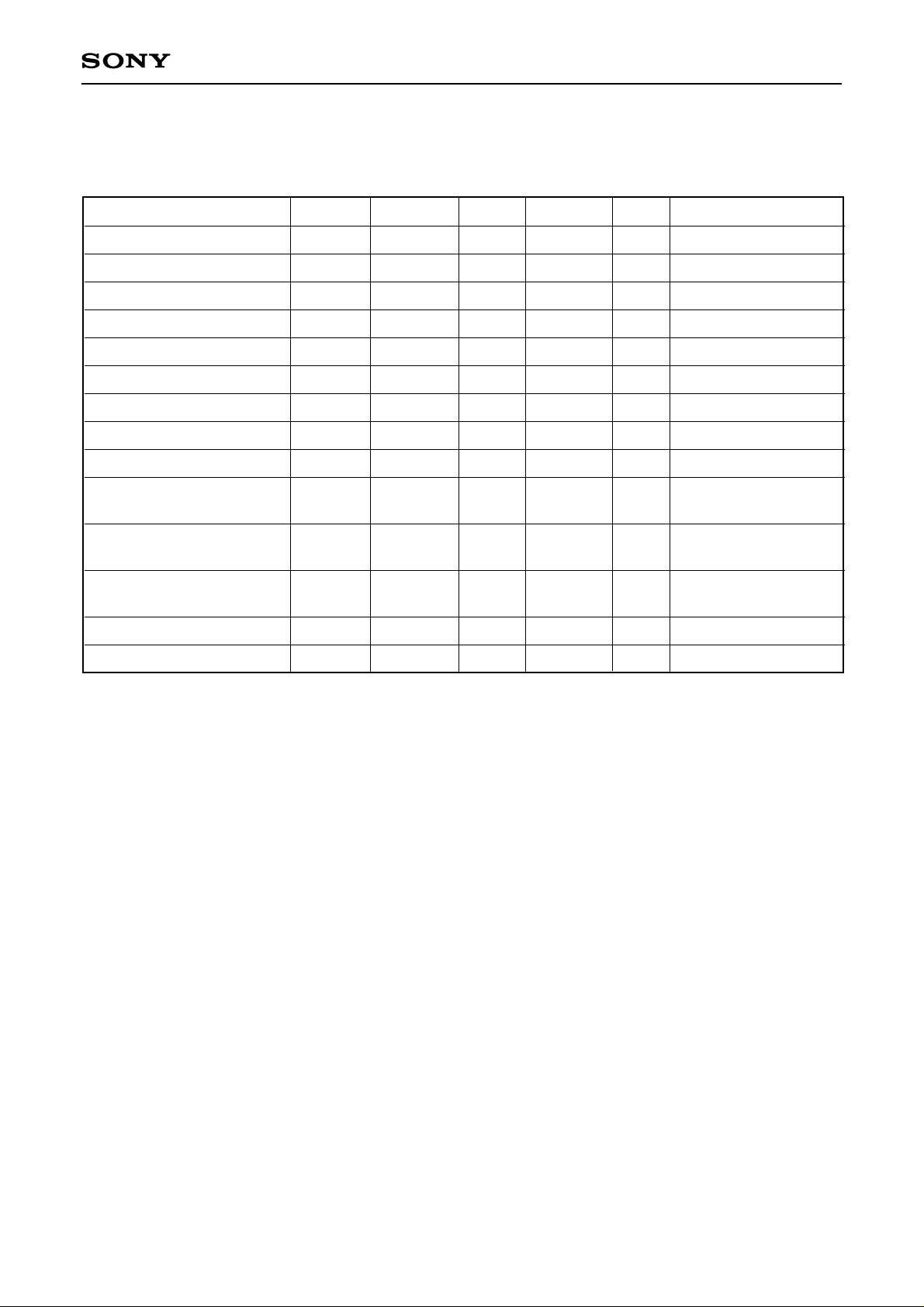
Electrical Characteristics
DC Characteristics (under the recommended operating conditions)
CXB1583Q
Item
TTL high level input voltage
TTL low level input voltage
TTL high level input current
TTL low level input current
TTL high level output voltage
TTL low level output voltage
ECL high level input voltage
ECL low level input voltage
ECL differential input voltage
ECL high level output voltage
ECL low level output voltage
ECL output amplitude
Current consumption
Power consumption
Symbol
VIH_T
VIL_T
IIH_T
IIL_T
VOH_T
VOL_T
VIH_E
VIL_E
VIS_E
VOH_E
VOL_E
VOS_E
ICC
PD
Min.
2
0
–400
2.2
VCC – 1.17
VCC – 1.81
200
VCC – 1.05
VCC – 1.81
650
Typ.
260
0.86
Max.
5.5
0.8
20
0.5
VCC – 0.88
VCC – 1.48
1000
VCC – 0.81
VCC – 1.55
341
1.18
Unit
V
V
µA
µA
V
V
V
V
mV
V
V
mV
mA
W
Conditions
VIH = VCC
VIL = 0
IOH = –0.4mA
IOL = 2mA
AC coupling input
50Ω terminated to
Vcc – 2 V
50Ω terminated to
Vcc – 2 V
50Ω terminated to
Vcc – 2 V
Output pins open
Output pins open
– 12 –
Page 13
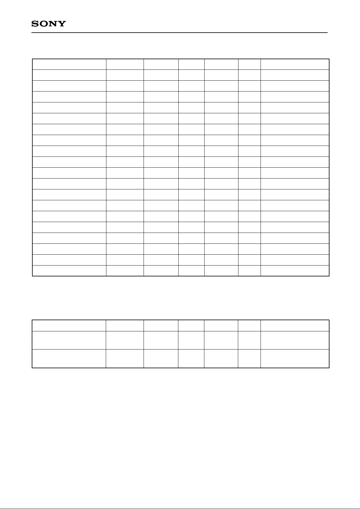
AC Characteristics (under the recommended operating conditions)
CXB1583Q
Item
PDI rise time
PDI fall time
REFCLK rise time
REFCLK fall time
TTL output rise time
TTL output fall time
ECL output rise time
ECL output fall time
SDIN data rate
REFCLK cycle tolerance
REFCLK duty cycle
PCLKOUT0 and 1 skew
PDI setup time
PDI hold time
PDO setup time
PDO hold time
Symbol
Tir_PDI
Tif_PDI
Tir_RFCK
Tif_RFCK
Tor_T
Tof_T
Tor_E
Tof_E
R_SDIN
Ttol_RFCK
DC_RFCK
Tskew
Ti_s
Ti_h
To_s
To_h
Min.
0.375
0.375
190
–200
40
–3
4
3
10
12
Typ.
0
Max.
10
10
5
5
5
5
500
500
280
200
60
3
Unit
ns
ns
ns
ns
ns
ns
ps
ps
Mbaud
ppm
%
ns
ns
ns
ns
ns
Conditions
0.8 to 2.0V
2.0 to 0.8V
0.8 to 2.0V
2.0 to 0.8V
0.8 to 2.0V, CL = 10pF
2.0 to 0.8V, CL = 10pF
20 to 80%, CL = 2pF
20 to 80%, CL = 2pF
SDIN cycle reference
REFCLK reference
REFCLK reference
PCLKOUT0 reference
PCLKOUT0 reference
TX deterministic jitter (p-p)
TX random jitter (p-p)
RX jitter tolerance
DJ
RJ
JT
0.08
0.15
0.7
PLL AC Characteristics (under the recommended operating conditions)
Item
TX/PX PLL frequency
acquisition time
RX PLL bit
synchronization time
Symbol Min. Typ.
Tfa
Tbs
Max.
500
2500
UI
UI
UI
Unit
µs
bit
Serial data output
Serial data output
Serial data input
Conditions
Loop damping
capacitance = 0.01µF
– 13 –
Page 14
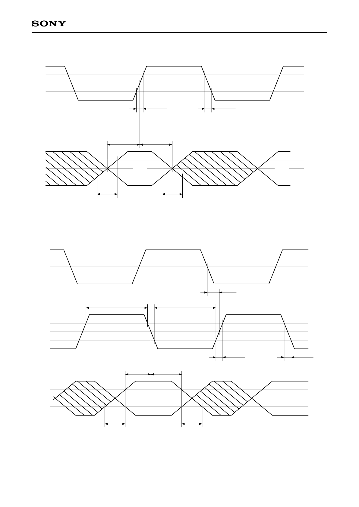
Timing Chart for TX
CXB1583Q
2.0V
1.5V
0.8V
REFCLK
PDI0 to 9
Timing Chart for RX
Tir_RFCK
Ti_hTi_s
Tir_PDI Tif_PDI
Tif_RFCK
2.0V
VALIDVALID
1.5V
0.8V
1.5V
PCLKOUT1
PCLKOUT0
PDO0 to 9
Th_PCK
Tor_PDO Tof_PDO
Tl_PCK
To_hTo_s
Tskew
2.2V
1.5V
0.6V
Tor_PCK Tof_PCK
2.2V
VALIDVALID
0.6V
– 14 –
Page 15
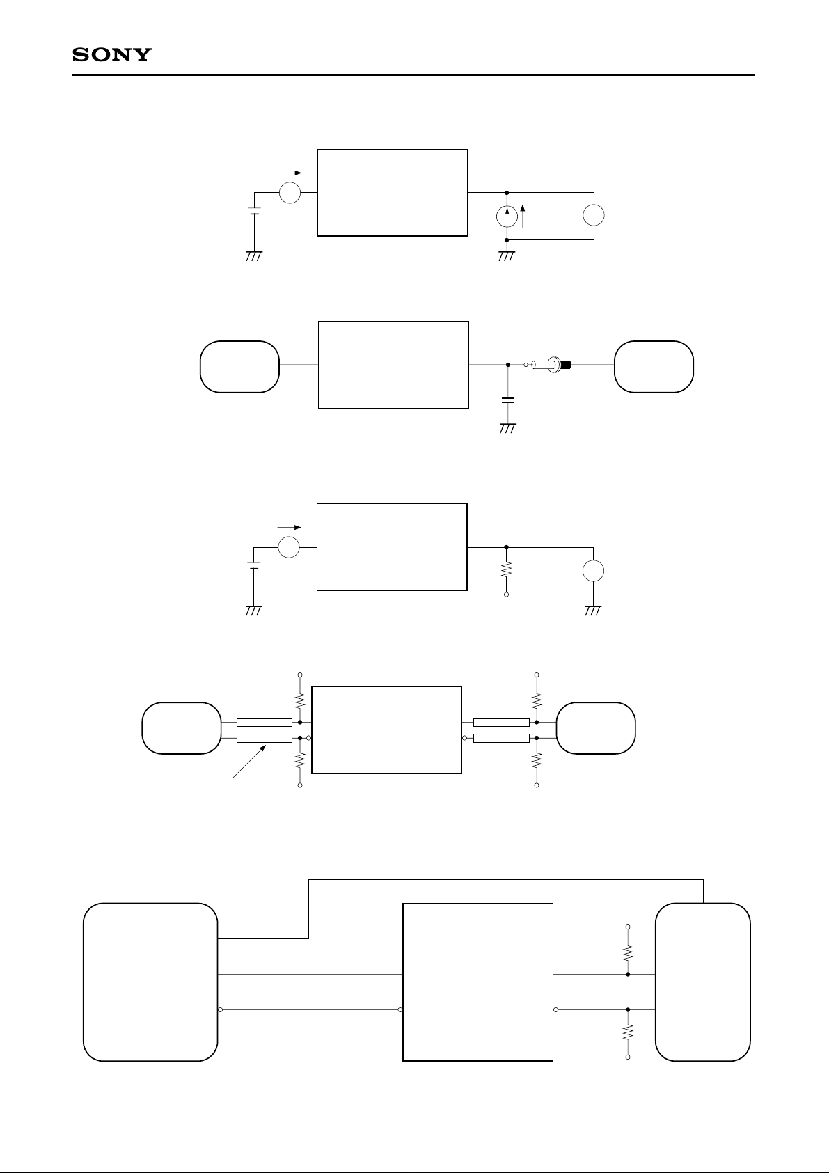
Electrical Characteristics Measurement Circuit
(See “Fig. 3 Power Supply Circuit” regarding the power supply.)
CXB1583Q
II_T
A
VI_T
Measurement device
TTL_IN
TTL_OUT
(a) TTL I/O DC characteristics measurement circuit
Measurement device
Pulse
generator
TTL_IN TTL_OUT
CL = 10 pF (including the probe capacitance)
(b) TTL I/O AC characteristics measurement circuit
II_E
A
VI_TE
Measurement device
ECL_IN ECL_OUT
CL
50Ω
IO_T
Probe
V
V
VO_T
VO_E
Oscilloscope
Pulse
generator
50Ω Transmission Line
Pulse pattern generator
VCCE – 2V
(c) ECL I/O DC characteristics measurement circuit
VCCE – 2V
50Ω
50Ω
VCCE – 2V
Measurement device
ECL_IN ECL_OUT
∗
ECL_IN
ECL_OUT
C ≤ 2 pF (input capacitance of the measurement
equipment and floating capacitance)
∗
VCCE – 2V
50Ω
50Ω
VCCE – 2V
(d) ECL I/O AC characteristics measurement circuit
6.640625MHz
265.625MBPS
Measurement device
SDIN SOUT
∗
SDIN
SOUT
Oscilloscope
265.625Mbps
∗
VCCE – 2V
50Ω
50Ω
Triger
Oscilloscope
(e) Jitter characteristics measurement circuit
– 15 –
V
CCE – 2V
Page 16

CXB1583Q
Notes on Operation
1. Clock synthesizer (PLL)
The CXB1583Q has a PLL-based clock synthesizer for generating the serial data transfer frequency
(transmission bit clock) and clock recovery circuit for recovering the clock from the reception serial data. These
circuits require the external loop filters and external resistors which determine the VCO center frequency. The
external part circuit and recommended constant values are shown in the figure below. The parasitic
capacitance attached to the pins which are used to connect external parts should be kept as small as possible
in order to obtain the good PLL characteristics.
52
C1
53
R2R1
C1 : 0.01µF
C2 : 0.01µF
R1 : 1.8kΩ
R2 : 1.8kΩ
R3 : 2.0kΩ
R4 : 2.0kΩ
R5 : 2.2kΩ
56
R5
58
59
R4R3
C2
Fig. 1. External Part Circuit and Recommended Constants
– 16 –
Page 17
CXB1583Q
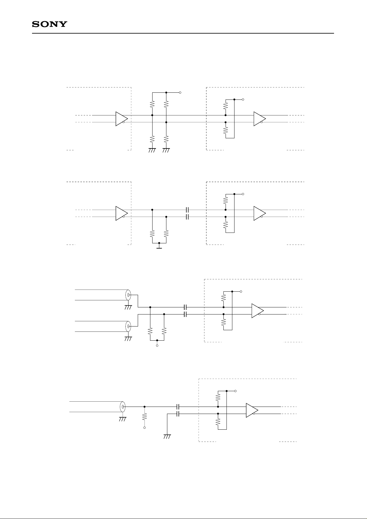
2. ECL input circuit
The ECL differential input pins are biased to VBB (VCC – 1.3 V) via an 18kΩ resistor in the IC. See the figures
below for ECL differential input methods.
VCC = 3.3V, VEE = GND
82Ω 82Ω
3.3V ECL output buffer ECL differential input buffer
VCC = 3.3V
V
CC = 3.3V, VEE = GND
18kΩ
18kΩ
V
BB (VCC – 1.3V)
(a) ECL differrential signal from 3.3V ECL output buffer
V
VCC = GND, VEE = –4.5V
0.01µF
0.01µF
330Ω
ECL100K output buffer ECL differential input buffer
330Ω
VEE
CC = 3.3V, VEE = GND
V
18kΩ
18kΩ
BB (VCC – 1.3V)
(b) ECL differrential signal from ECL 100K output buffer
CC = 3.3V, VEE = GND
V
18kΩ
18kΩ
ECL differential input buffer
50Ω
TRANS.
LINE
0.01µF
0.01µF
50Ω 50Ω
VTT (VCC – 2V)
(c) ECL differrential signal from 50Ω transmission line
CC = 3.3V, VEE = GND
V
18kΩ
18kΩ
ECL differential input buffer
50W
TRANS.
LINE
50Ω
VTT (VCC – 2V)
0.01µF
0.01µF
BB (VCC – 1.3V)
V
BB (VCC – 1.3V)
V
(d) ECL single signal from 50Ω transmission line
Fig. 2. ECL Input Circuits
– 17 –
Page 18

3. Example of power supply circuit
CXB1583Q
VCCG
VCCE
EEG
V
VEEE
VCCP
0.1µF22µF0.1µF22µF
EEP
V
3.3V
CCT
V
0.1µF22µF
EET
V
Fig. 3. Example of power supply circuit
4. Power-on reset signal (POR∗)
The CXB1583Q has the power-on reset signal (POR∗). This signal functions as a system reset signal when the
power is turned on, the low level of signal is output for approximately 100ns and then the high level results.
POR∗ Output
Tpor
Power On
Fig. 4. Power-on reset signal
– 18 –
Page 19
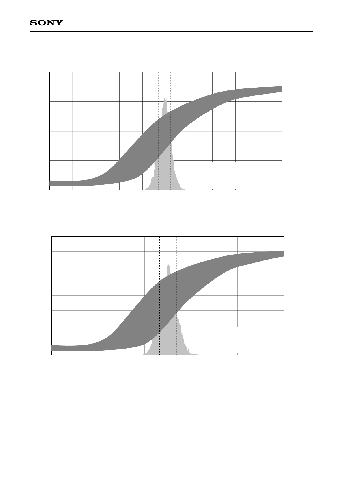
Example of Representative Characteristics
Example of Rj measurement (RX recovered clock, 266MHz operation)
[ 100mV/div ]
CXB1583Q
TX input (PDI0 to 9): Random data
RX input (SDIN): ±K28.5
Ta = 27°C
Rj = 26.3ps (RMS)
[ 100mV/div ]
[ 100ps/div ]
Example of Rj measurement (RX recovered clock, 200MHz operation)
TX input (PDI0 to 9): Random data
RX input (SDIN): ±K28.5
Ta = 27°C
Rj = 36.9ps (RMS)
[ 100ps/div ]
– 19 –
Page 20

[ 100mV/div ]
CXB1583Q
Example of Rj measurement (SDOUT, 266Mbps operation)
TX input (PDI0 to 9): Random data
Ta = 27°C
Rj = 17.6ps (RMS)
[ 100mV/div ]
[ 100ps/div ]
Example of Rj measurement (SDOUT 200Mbps operation)
TX input (PDI0 to 9): Random data
Ta = 27°C
Rj = 24.3ps (RMS)
[ 100ps/div ]
– 20 –
Page 21
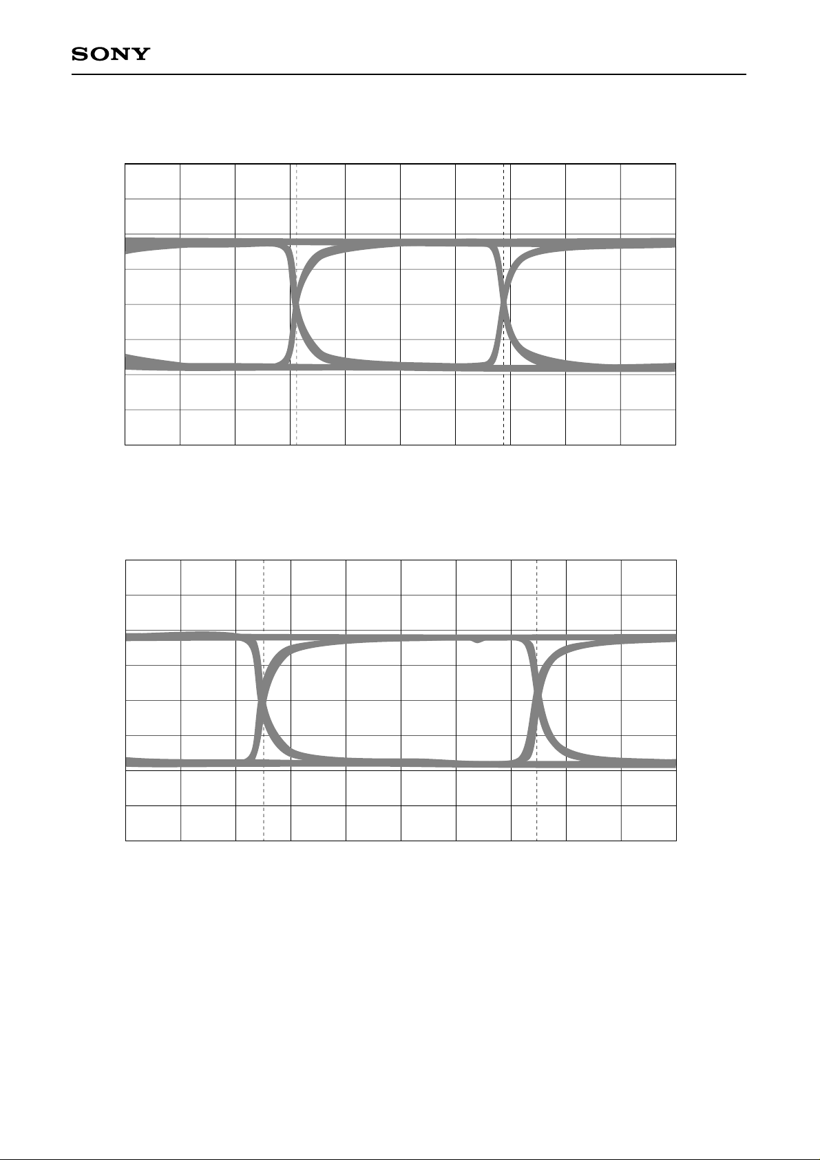
[ 200mV/div ]
CXB1583Q
Eye pattern (TX SDOUT, 266Mbps operation)
Ta = 27°C
[ 200mV/div ]
[ 1ns/div ]
Eye pattern (TX SDOUT, 200Mbps operation)
Ta = 27°C
[ 1ns/div ]
– 21 –
Page 22

[ 200mV/div ]
CXB1583Q
Eye pattern (RX retimed data, 266Mbps operation)
Ta = 27°C
[ 200mV/div ]
[ 1ns/div ]
Eye pattern (RX retimed data, 200Mbps operation)
Ta = 27°C
[ 1ns/div ]
– 22 –
Page 23

Package Outline Unit: mm
16.0 ± 0.4
14.0 – 0.1
60
+ 0.4
80PIN QFP (PLASTIC)
41
+ 0.35
1.5 – 0.15
+ 0.1
0.127 – 0.05
CXB1583Q
0.1
61
80
1
0.65
SONY CODE
EIAJ CODE
JEDEC CODE
+ 0.15
0.3 – 0.1
QFP-80P-L03
LQFP080-P-1414
40
21
20
± 0.12
M
PACKAGE STRUCTURE
PACKAGE MATERIAL
LEAD TREATMENT
LEAD MATERIAL
PACKAGE WEIGHT
(15.0)
+ 0.15
0.1 – 0.1
0° to 10°
EPOXY RESIN
SOLDER PLATING
COPPER / 42 ALLOY
0.6g
0.5 ± 0.2
– 23 –
 Loading...