

Page 1
Description
The CXB1563Q achieves the 2R optical-fiber
communication receiver functions (Reshaping and
Regenerating) on a single chip. This IC is also
equipped with the signal interruption alarm output
function, which is used to discriminate the existence
of data input.
Features
• Auto-offset canceler circuit
• Signal interruption alarm output
• 2-level switching function of identification maximum voltage amplitude for alarm block
• Single 5V power supply
Applications
• SONET/SDH : 622.08Mb/s
• Fiber channel : 531.25Mb/s
Absolute Maximum Ratings
• Supply voltage VCC – VEE –0.3 to +7.0 V
• Storage temperature Tstg –65 to +150 °C
• Input voltage difference : I VD – VD I Vdif 0.0 to +2.5 V
• SW input voltage Vi VEE to VCC V
• Output current (Continuous) IO 0 to 50 mA
(Surge current) 0 to 100 mA
Recommended Operating Conditions
• Supply voltage VCC – VEE 5.0±0.5 V
• Termination voltage (for data/alarm) VCC – VT1 1.8 to 2.2 V
• Termination voltage (for alarm 2) VT2 VEE V
• Termination resistance (for data/alarm)RT1 45 to 55 Ω
• Termination resistance (for alarm 2) RT2 460 to 560 Ω
• Operating temperature Ta –40 to +85 °C
Structure
Bipolar silicon monolithic IC
– 1 –
CXB1563Q
E95710A6Z
2R IC for Optical Fiber Communication Receiver
Sony reserves the right to change products and specifications without prior notice. This information does not convey any license by
any implication or otherwise under any patents or other right. Application circuits shown, if any, are typical examples illustrating the
operation of the devices. Sony cannot assume responsibility for any problems arising out of the use of these circuits.
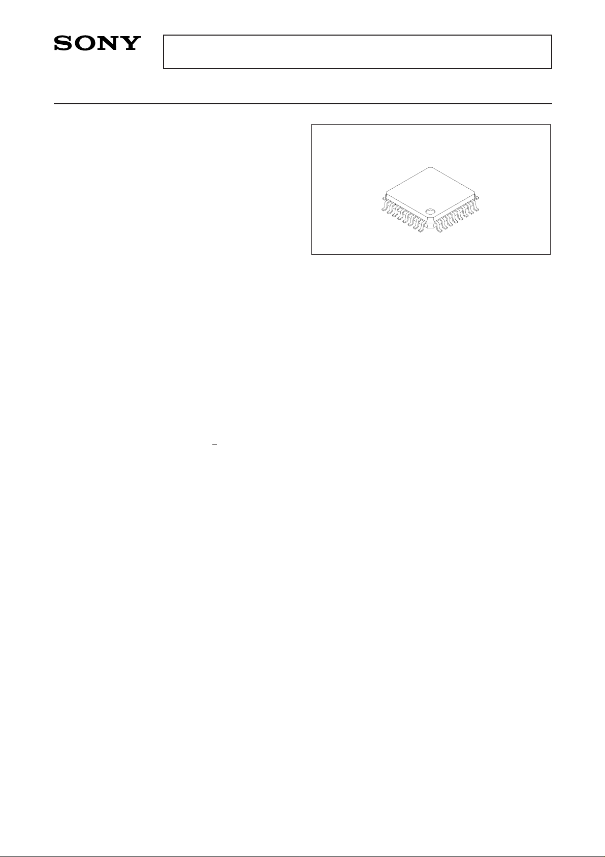
32 pin QFP (Plastic)
Page 2
– 2 –
CXB1563Q
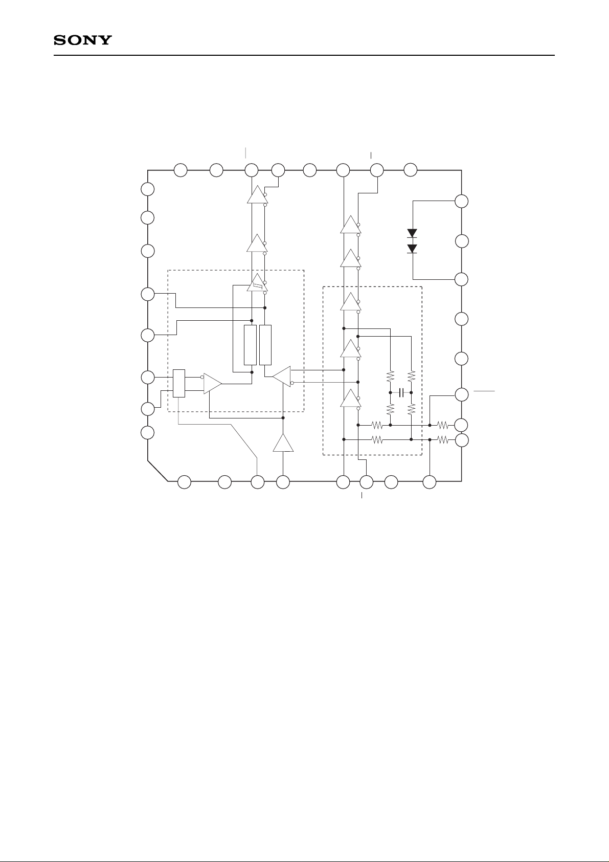
Block Diagram and Pin Configuration
2
3
4
5
6
7
8
9
10
11
12
13
14
15
16
17
18
19
20
21
22
23
24
25
26
27
28
29
30
31
32
1
peak hold
∆V
peak hold
Alarm
Block
Limiting
Amplifier
Block
R1
R1
R2
R2
Q
VccDA
SD
Q
SD
VccD
VccDA
N.C.
N.C.
CAP3
CAP2
DOWN
UP
VccA
TM
VccD
V
EED
VccA
V
EEA
CAP1
R2K
R1K
VccA
VccA
V
EE
I
SW
D
D
CAP1
N.C.
R3
R4
V
CC
A
N.C.
Page 3

– 3 –
CXB1563Q
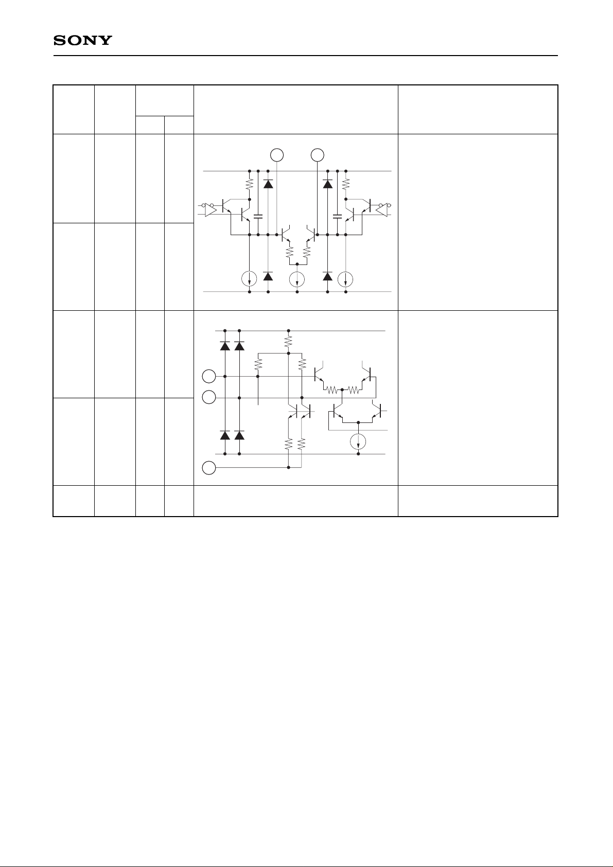
Pin Description
Pin No.
1,2
VCCA
0V
Positive power supply for analog
block.
Switches the identification
maximum voltage amplitude.
High voltage when open; the
identification maximum voltage
amplitude becomes 50mVp-p.
Low voltage when connecting
this pin to VEE; the amplitude
becomes 20mVp-p.
3 VEEI –5V
4
SW
0V
(OPEN)
or
–5V
Limiting amplifier block input.
Be sure to make this input with
AC coupled.
Positive power supply for analog
block.
Pins 8 and 11 connect a
capacitor which determines the
cut-off frequency for feedback
block, and 1kΩ is connected
between Pins 8 and 9; 2kΩ
between Pins 10 and 11. A
resistor which is to be inserted in
parallel with a capacitor can be
selected 5 ways by external
wiring, and DC feedback can be
varied.
5
D
–
1.3V
–
0.9V
to
–
1.7V
–
0.9V
to
–
1.7V
6
D
–
1.3V
7
VCCA
0V
8
CAP1
–
1.8V
9
R1K
10
R2K
11
CAP1
–
1.8V
Generates the default voltage
between UP and DOWN.
The voltage (8.0mV for input
conversion) can be generated
between UP and DOWN
(Pins 30 and 31) as alarm
setting level by connecting this
pin to VEEA.
Symbol
Typical pin
voltage (V)
DC
AC
Equivalent circuit
Description
150k
100k
V
REF
VEEA
V
CCA
4
31
30
VccA
V
EEA
SW
993
110.3
110.3
Vcs
3
VCCA
V
EEA
200
200
1.5k
1.5k
10k
10k
100p
200
200
2k
1k
5
6
11
10
9
8
Page 4

– 4 –
CXB1563Q
12
13
14
15
VEEA
VCCA
VEED
VCCD
–5V
0V
–5V
0V
–
0.9V
to
–
1.7V
Negative power supply for
analog block.
Positive power supply for analog
block.
Negative power supply for digital
block.
Positive power supply for digital
block.
16
TM
–
3.4V
18
Q
–
0.9V
to
–
1.7V
19
Q
Positive power supply for output
buffer.
20
VCCDA
Chip temperature monitor.
17
N.C
No connected.
Data signal output.
Terminate this pin in 50Ω at
VTT = –2V.
–
0.9V
to
–
1.7V
21
SD
Alarm signal output.
Terminate this pin in 50Ω at
VTT = –2V.
DC
AC
14
16
–
0.9V
to
–
1.7V
22
SD
23
24
25
26
27
VccDA
VccD
N.C
N.C
N.C
Positive power supply for digital
block.
Positive power supply for digital
block.
No connected.
0V
0V
0V
VEED
V
CCDA
19
18
VEED
V
CCDA
21
22
Pin No.
Symbol
Typical pin
voltage (V)
Equivalent circuit
Description
Page 5
– 5 –
CXB1563Q
DC
AC
28
CAP3
–
1.8V
29
CAP2
–
1.8V
Connects a peak hold circuit
capacitor for alarm block. 470pF
should be connected to VccA
each.
CAP2 pin → Peak hold
capacitor connection for
alarm level setting block.
CAP3 pin → Peak hold
capacitor connection for
limiting amplifier signal.
10p
10p
VCCA
V
EEA
80
5µA
5µA
80
29
28
30
DOWN
–
0.84V
(for
VEEI
= –5V)
31
UP
–
0.8V
(for
VEEI
= –5V)
32
VccA
0V
Positive power supply for analog
block.
Connects a resistor for alarm
level setting.
Default voltage can be
generated without an external
resistor by shorting the VEEI pin
to VEEA.
31
30
VccA
V
EEA
SW
993
110.3
110.3
Vcs
3
Pin No.
Symbol
Typical pin
voltage (V)
Equivalent circuit
Description
Page 6

– 6 –
CXB1563Q
Power supply
Q/Q SD/SD High output voltage
Q/Q SD/SD Low output voltage
SD/SD High output voltage 2
SD/SD Low output voltage 2
SW High input voltage
SW Low input voltage
SW High input current
SW Low input current
D/D input resistance
Internal resistance 1 for alarm level
setting
Internal resistance 2 for alarm level
setting
Pare ratio of internal resistance 2 for
alarm level setting
Resistance between CAP1 and R1K
Resistance between CAP1 and R2K
Electrical Characteristics
• DC characteristics
(VCC = GND, VEE = –5V±10%, Ta = –40 to +85°C, VCC = VCCD, VCCDA, VCCA VEE = VEED, VEEA)
Item
IEE
VOH
VOL
VOHb
VOLb
VIH
VIL
IIH
IIL
Rin
Ra1
Ra2A, B
δRa2
R3
R4
RT1 = 50Ω,
VT1 = –2V termination
RT1 = 50Ω,
VT1 = –2V termination,
Ta = 0 to 85°C
RT2 = 510Ω,
VEE termination,
Ta = 0 to 85°C
Refer to Fig. 3.
Refer to Fig. 3.
Ra2A/Ra2B
–50
–1025
–1810
–1075
–1860
–1900
VEE
–60
1125
745
82.7
0.97
745
1489
–37
1500
993
110.3
993
1986
–28
–880
–1620
–830
–1570
0
–2500
2
1875
1241
137.9
1.03
1241
2482
mA
mV
µA
Ω
Ω
Symbol Min. Typ. Max. UnitConditions
Page 7
– 7 –
CXB1563Q
Maximum input voltage amplitude
Amplifier gain
(in Limiting Amplifier)
Identification maximum voltage
amplitude of alarm level
Hysteresis width
SD response assert time
SD response deassert time
SD response assert time for alarm
level default
SD response deassert time for
alarm level default
Alarm setting level for default
Propagation delay time
Q/Q rise time
Q/Q fall time
SD/SD rise time
SD/SD fall time
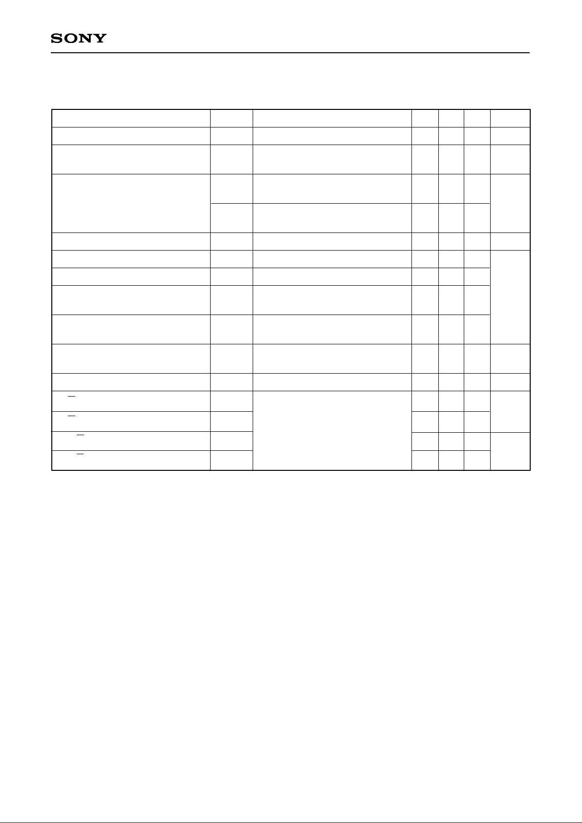
• AC characteristics
(VCC = GND, VEE = –5V±10%, Ta = –40 to +85°C, VCC = VCCD, VCCDA, VCCA VEE = VEED, VEEA)
Item
Vmax
Gv
VminA1
VminA2
∆P
Tas
Tdas
Tasd
Tdasd
Vdef
TPD
Tr_Q
Tf_Q
Tr_SD
Tf_SD
Single-ended input
SW pad: Low,
single-ended input
SW pad: Open High,
single-ended input
Low → High
∗1
High → Low
∗2
Low → High
∗3
High → Low
∗4
UP/DOWN pins; Open,
connect VEEI to VEE.
D to Q
RT1 = 50Ω, VT1 = –2V termination,
VEE = –5V, Ta = 0 to 85°C
20% to 80%
1600
40
20
50
4
0
2.3
0
2.3
6.6
0.4
250
250
0.45
0.45
6
8.0
1.0
7
100
100
100
100
9.3
1.6
450
450
1.6
1.6
mVp-p
dB
mVp-p
dB
µs
mV
ns
ps
ns
Symbol
Min. Typ. Max. Unit
Conditions
∗1
VUP – VDOWN = 100mV, Vin = 100mVp-p (single ended), SW pin: High
Peak hold capacitance (CAP2, CAP3 pins) of 470pF; connect VEEI to VEE.
∗2
VUP – VDOWN = 100mV, Vin = 1Vp-p (single ended), SW pin: High
Peak hold capacitance (CAP2, CAP3 pins) of 470pF; connect VEEI to VEE.
∗3
Vin = 50mVp-p (single ended), SW pin: Low
Peak hold capacitance (CAP2, CAP3 pins) of 470pF; connect VEEI to VEE.
∗4
Vin = 1Vp-p (single ended), SW pin: Low
Peak hold capacitance (CAP2, CAP3 pins) of 470pF; connect VEEI to VEE.
Page 8
– 8 –
CXB1563Q
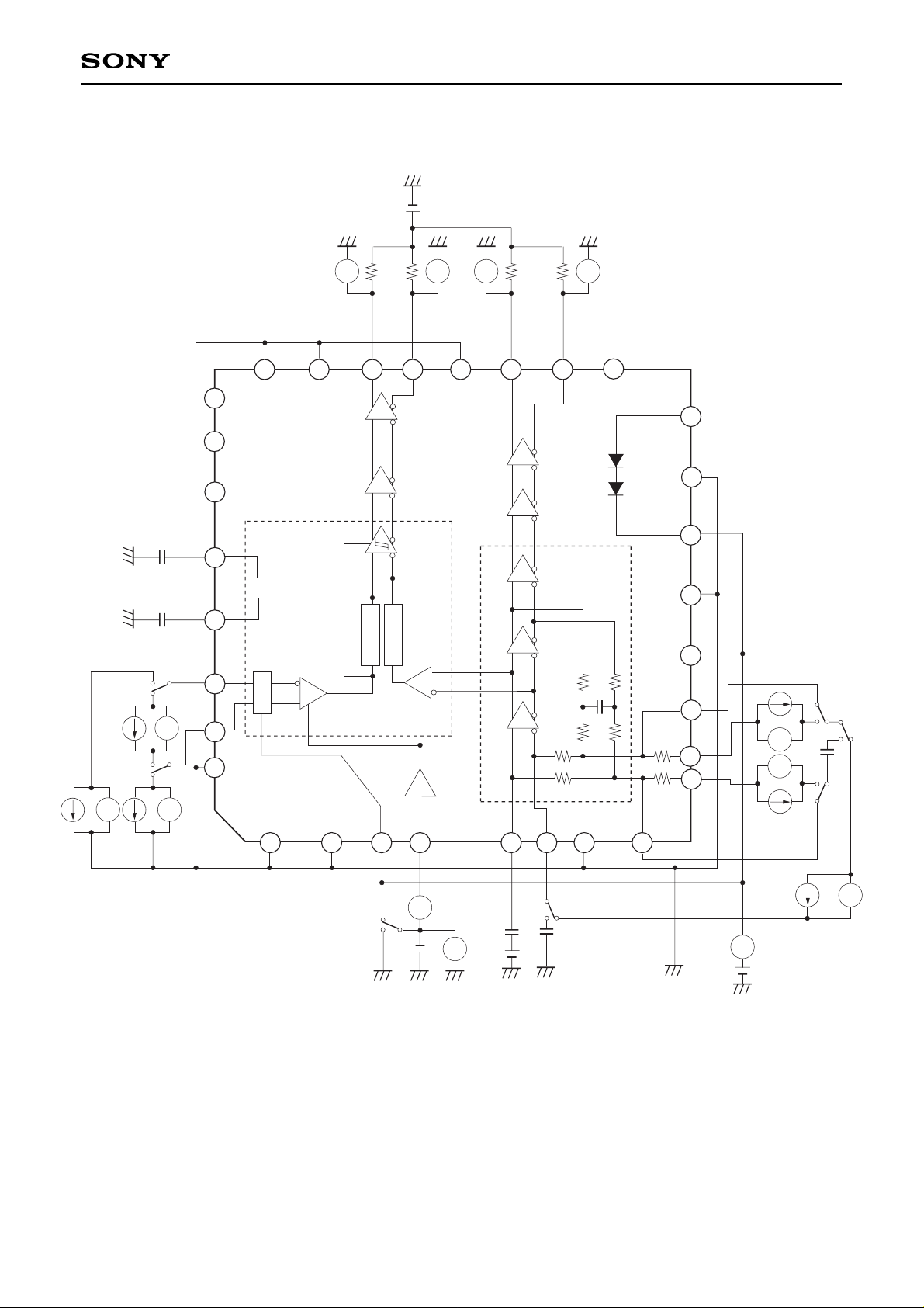
DC Electrical Characteristics Measurement Circuit
V V V
V
51
51
51 51
C3
C3
V
V
V
V
VS
VD
C1
C1
A
VEE
–5V
V
C2
V
–2V
V
T1
V
A
2
3
4
5
6
7
8
9
10
11
12
13
14
15
16
17
18
19
20
21
22
23
24
25
26
27
28
29
30
31
32
1
peak hold
∆V
peak hold
Alarm
Block
Limiting
Amplifier
Block
R1
R1
R2
R2
R3
R4
Page 9
– 9 –
CXB1563Q
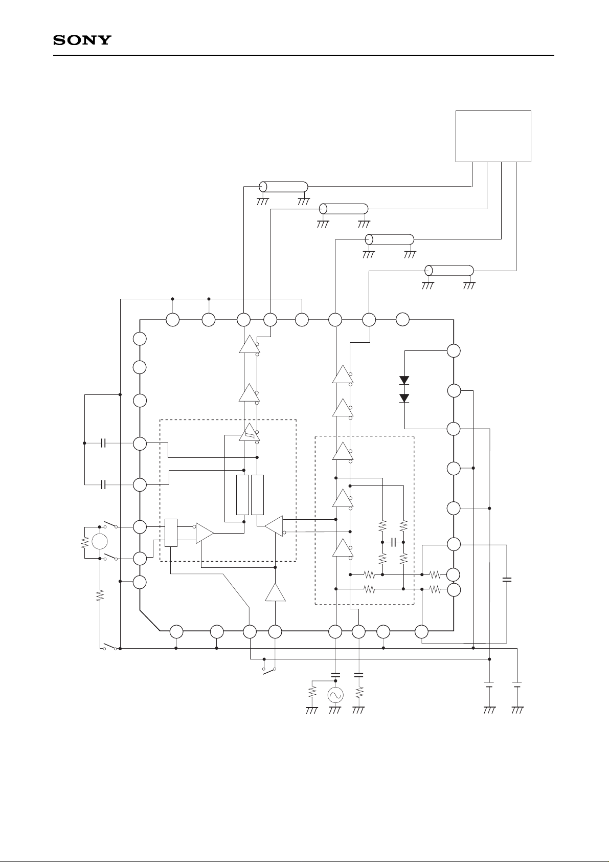
AC Electrical Characteristics Measurement Circuit
Z0 = 50
Z0 = 50
Z0 = 50
Z0 = 50
Oscilloscope
50Ω input
0.22µF
0.022µF
0.022µF
VEE VCC
–3V
+2V
V
REX1
REX2
470pF
470pF
2
3
4
5
6
7
8
9
10
11
12
13
14
15
16
17
18
19
20
21
22
23
24
25
26
27
28
29
30
31
32
1
peak hold
∆V
peak hold
Alarm
Block
Limiting
Amplifier
Block
R1
R1
R2
R2
R3
R4
51
51
Page 10

– 10 –
CXB1563Q
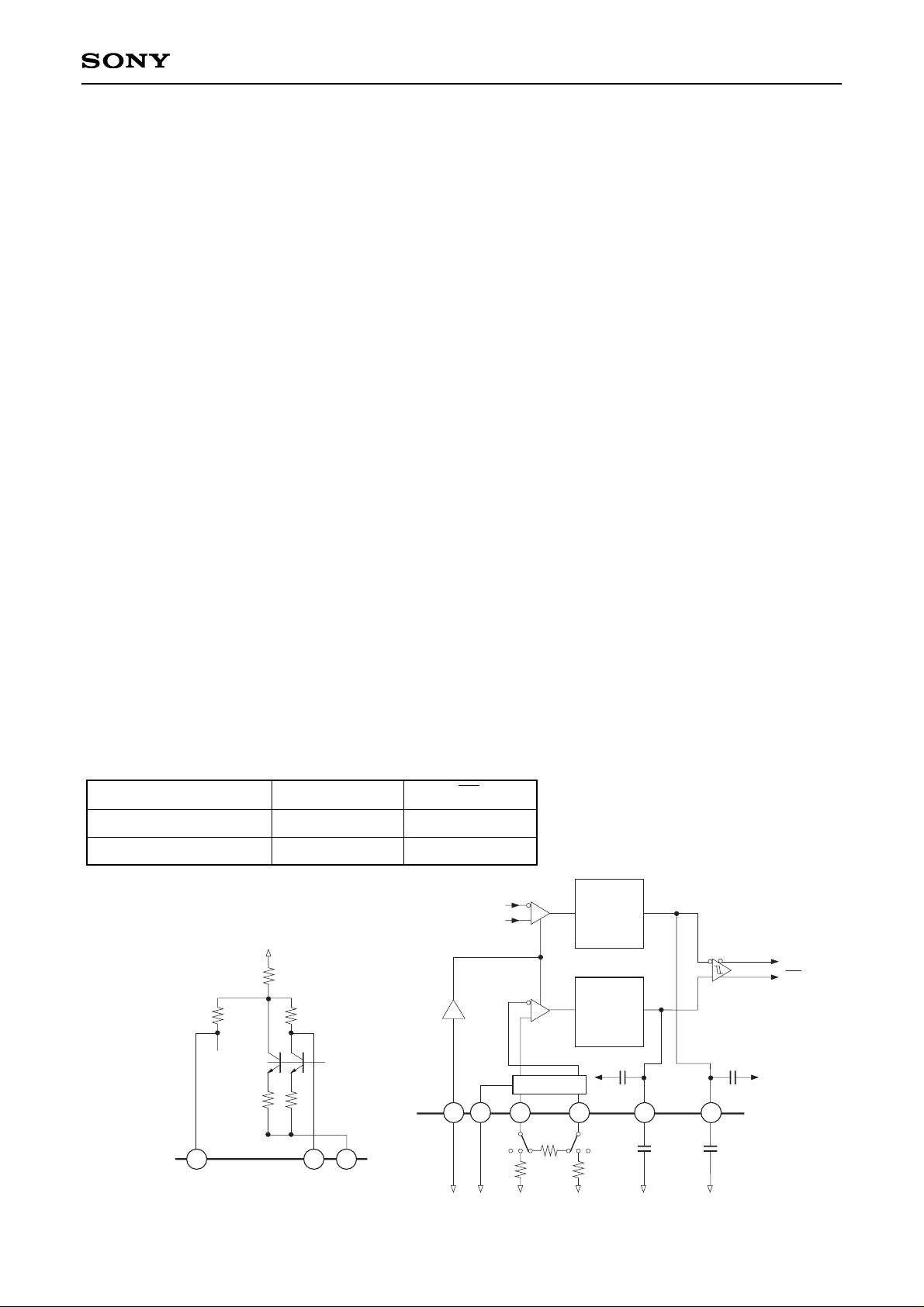
Application Circuit
C2
0.22µF
C1
0.022µF
VEE
–5V
C3
470pF
C1
0.022µF
C3
470pF
5151 51 51
VT1 –2V
2
3
4
5
6
7
8
9
10
11
12
13
14
15
16
17
18
19
20
21
22
23
24
25
26
27
28
29
30
31
32
1
peak hold
∆V
peak hold
Alarm
Block
Limiting
Amplifier
Block
R1
R1
R2
R2
R3
R4
51
51
Application circuits shown are typical examples illustrating the operation of the devices. Sony cannot assume responsibility for
any problems arising out of the use of these circuits or for any infringement of third party patent and other right due to same.
Page 11

– 11 –
CXB1563Q
C1
C1
C2
R1 R1
R2
R2
To IC interior
D
R3
R4
5
6
8
9
10
11
Fig. 1
f1 f2
Frequency
Gain
Feedback
frequency response
Amplifier
frequency response
Fig. 2
Notes on Operation
1. Limiting amplifier block
The limiting amplifier block is equipped with the auto-offset canceler circuit. When external capacitors C1 and
C2 are connected as shown in Fig. 1, the DC bias is set automatically in this block. External capacitor C1 and
IC internal resistor R1 determine the low input cut-off frequency f2 as shown in Fig. 2. Similarly, external
capacitor C2 and IC internal resistor R2 determine the high cut-off frequency f1 for DC bias feedback. Since
peaking characteristics may occur in the low frequency area of the amplifier gain characteristics depending on
the f1/f2 combination, set the C1 and C2 so as to avoid the occurrence of peaking characteristics. The target
values of R1 and R2 and the typical values of C1 and C2 are as indicated below. When a single-ended input is
used, provide AC grounding by connecting Pin 6 to a capacitor which has the same capacitance as capacitor
C1.
R1 (internal): 1.5kΩ R2 (internal): 10kΩ
f2: 4.8kHz f1: 72Hz
C1 (external): 0.022µF C2 (external): 0.22µF
1kΩ is incorporated between Pins 8 and 9; 2kΩ between Pins 10 and 11. A resistance value which is to be
inserted in parallel with a capacitor f2 can be selected 5 ways (∞, 3kΩ, 2kΩ, 1kΩ, 1k//2kΩ) by external wiring,
and DC feedback can be varied.
Page 12
– 12 –
CXB1563Q
2. Alarm block
In order to operate the alarm block, give the voltage difference between Pins 30 and 31 to set an alarm level
and connect the peak hold capacitor C3 shown in Fig. 3.
This IC has two setting methods of alarm level; one is to connect VEE to Pin 3 and leave Pins 30 and 31 open
to set an alarm level default value (8mV for input conversion). The other is to connect Pin 3 to VEE and set a
desired alarm level using the external resistors REX1 and REX2 and REX3 shown in Fig. 3.
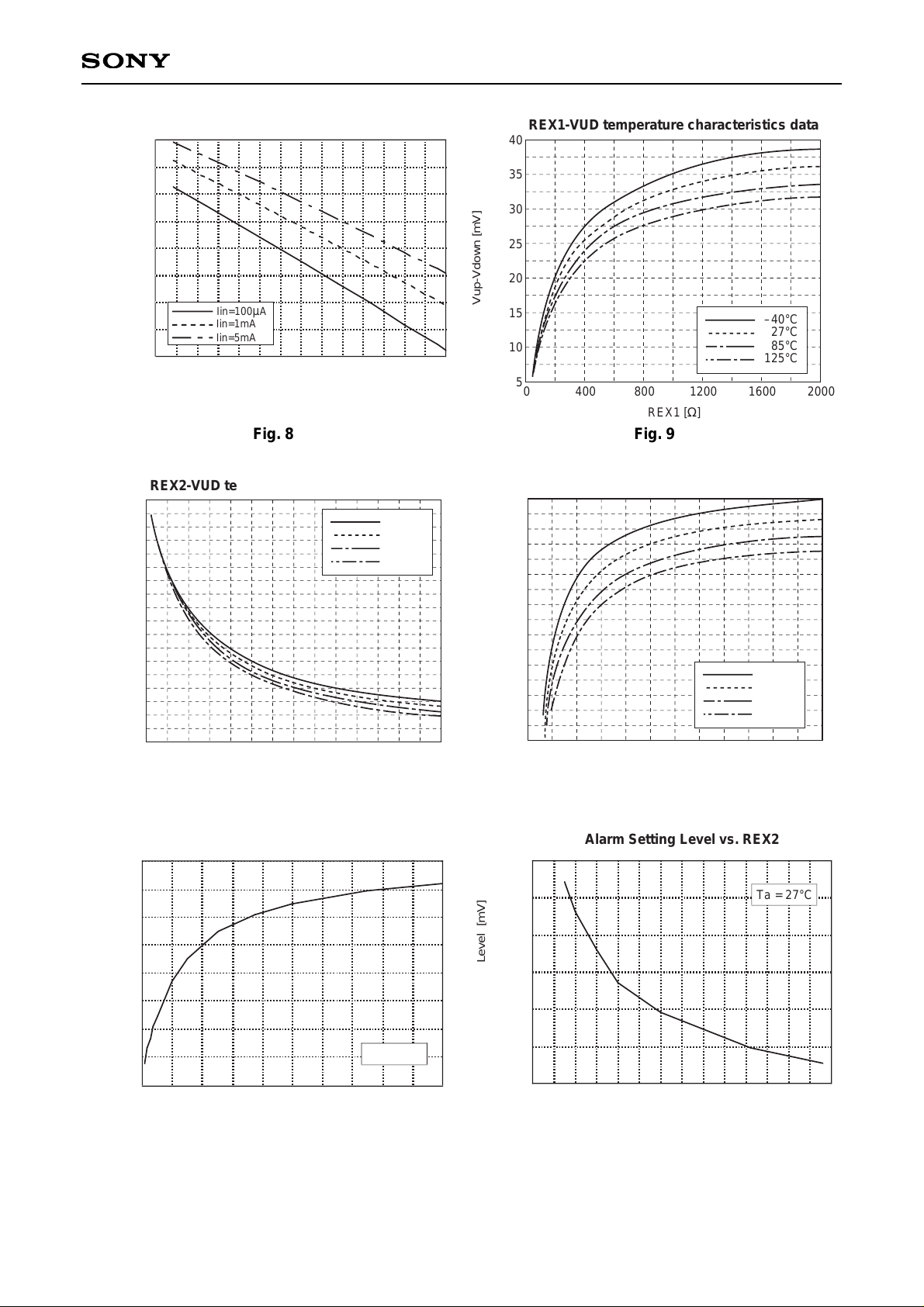
Connect REX1 between Pins 30 and 31, or between Pin 30 and VCC when less alarm level is desired to be set
than its default value; connect REX2 between Pin 31 and Vcc potential when more alarm level is desired to be
set than its default value. However, the Pin 31 voltage must be higher than that of Pin 30. Refer to Figs. 5, 8 to
13 for this alarm level setting.
This IC also features two-level setting of identification maximum voltage amplitude. The amplitude is set to
50mVp-p when Pin 4 is left open (High level) and it is set to 20mVp-p when Pin 4 is Low level. Therefore, noise
margin can be increased by setting Pin 4 to Low level when small signal is input. The relation of input voltage
and peak hold output voltage is shown in Fig. 6.
In the relation between the alarm setting level and hysteresis width, the hysteresis width is designed to
maintain a constant gain (design target value: 6dB) as shown in Fig. 4. The C3 capacitance value should be
set so as to obtain desired assert time and deassert time settings for the alarm signal.
The electrical characteristics for the SD response assert and deassert times are guaranteed only when the
waveforms are input as shown in the timing chart of Fig. 7.
The typical values of REX1, REX2, REX3 and C3 are as follows: (Approximately 10pF capacitor is built in Pins 28
and 29 each.)
REX1 : 217Ω (when the alarm level is set to 4mV for input conversion.)
REX2 : 634Ω (when the alarm level is set to 19mV for input conversion.)
REX3 : 4kΩ (when the alarm level is set to 4mV for input conversion.)
C3 : 470pF
The table below shows the alarm logic.
From
Limiting Amplifier
Peak hold
SD
SD
VccA
10p
VccA
10p
Vcc
C3
Vcc
Peak hold
Ra2B
110.3
Ra1
VCCA
IC interior
IC exterior
Ra1, Ra2A and Ra2B values
are typical values.
C3
30
31
Ra2A
110.3
993
Vcs
∆V
31
30
29
28
Vcc
R
EX1
REX2
3
4
3
Vcc
REX3
Optical signal input state
Signal input
Signal interruption
High level
Low level
Low level
High level
SD SD
Fig. 3
Page 13

– 13 –
CXB1563Q
3dB 3dB
Alarm setting
input level
Hysteresis
Input electrical signal amplitude
SD output
High
level
Low
level
Small Large
V
DAS VAS
VDAS → Deassert level
VAS → Assert level
VAS
VDAS
V
AS
, V
DAS
[mV]
Voltage between Pins 30 and 31 [mV]
25
20
15
10
5
0
0
20 40 60
80
100
AAA
SW = High
SW = Low
Fig. 4 Fig. 5
Peak hold output voltage
0 2
0
5
0
Input voltage [mVp-p]
SW → Open High
SW → Low
Fig. 6
Assert time
Alarm setting level
Hysteresis width
Data input
(D)
Deassert time
Data output
(Q)
Alarm output
(SD)
Fig. 7
Page 14
– 14 –
CXB1563Q
3. Others
Pay attention to handling this IC because its electrostatic discharge strength is weak.
1000
1200
1400
1600
1800
–50 –25 0 25 50 75 100 125
Tj [°C]
TM-V
EE
[mV]
TM pin temperature characteristics
Iin=100µA
Iin=1mA
Iin=5mA
REX1 [Ω]
0 2000400 800 1200 1600
5
40
35
30
25
20
15
10
Vup-Vdown [mV]
–40°C
27°C
85°C
125°C
REX1-VUD temperature characteristics data
Fig. 8 Fig. 9
REX2-VUD temperature characteristics data
REX2 [Ω]
0 70001000 3000 4000 5000
40
130
120
110
100
90
80
60
Vup-Vdown [mV]
2000
50
–40°C
27°C
85°C
125°C
6000
70
REX3 [kΩ]
0 305 15 20 25
0
40
35
30
25
20
15
10
Vup-Vdown [mV]
–40°C
27°C
85°C
125°C
10
5
REX3-VUD temperature characteristics data
Fig. 10 Fig. 11
Fig. 12 Fig. 13
0
2
4
6
8
0 400 800 1200 1600 2000
REX1 [Ω]
Alarm Setting Level [mV]
Alarm Setting Level vs. REX1
Ta = 27°C
10
12
14
16
18
20
22
0 1000 2000 3000 4000 5000 6000 7000
REX2 [Ω]
Alarm Setting Level [mV]
Alarm Setting Level vs. REX2
A
A
A
A
A
A
Ta = 27°C
Page 15

– 15 –
CXB1563Q
Example of Representative Characteristics
10
–9
10
–8
10
–7
10
–6
10
–5
10
–4
1.8 2 2.2 2.4 2.6 2.8 3
Data Input Level [mVp-p]
Bit Error Rate
Bit Error Rate vs. Data Input Level
10
–11
10
–10
VEE = –5.0V
Ta = 27°C
D = 622.08Mbps
pattern : PRBS2
23
–1
0
10
20
30
40
50
60
70
80
1 10 100 1000
Data Input Level [mVp-p]
Output RMS Jitter [pS]
Output RMS Jitter vs. Data Input Level
VEE = –5.0V
Ta = 27°C
D = 622.08Mbps
pattern: PRBS2
23
–1
Fig. 14
Q Output Waveform
VEE = –5.0V
Ta = 27°C
D = 622.08Mbps
Vin = 3mVp-p, Single Input
pattern : PRBS2
23
–1
22.3500ns19.8500ns 24.8500ns
Ch. 1 = 200.0mV/div
Timebase = 500ps/div
Offset = 680.0mV
Delay = 22.3500ns
Fig. 16
Fig. 15
Page 16
– 16 –
CXB1563Q
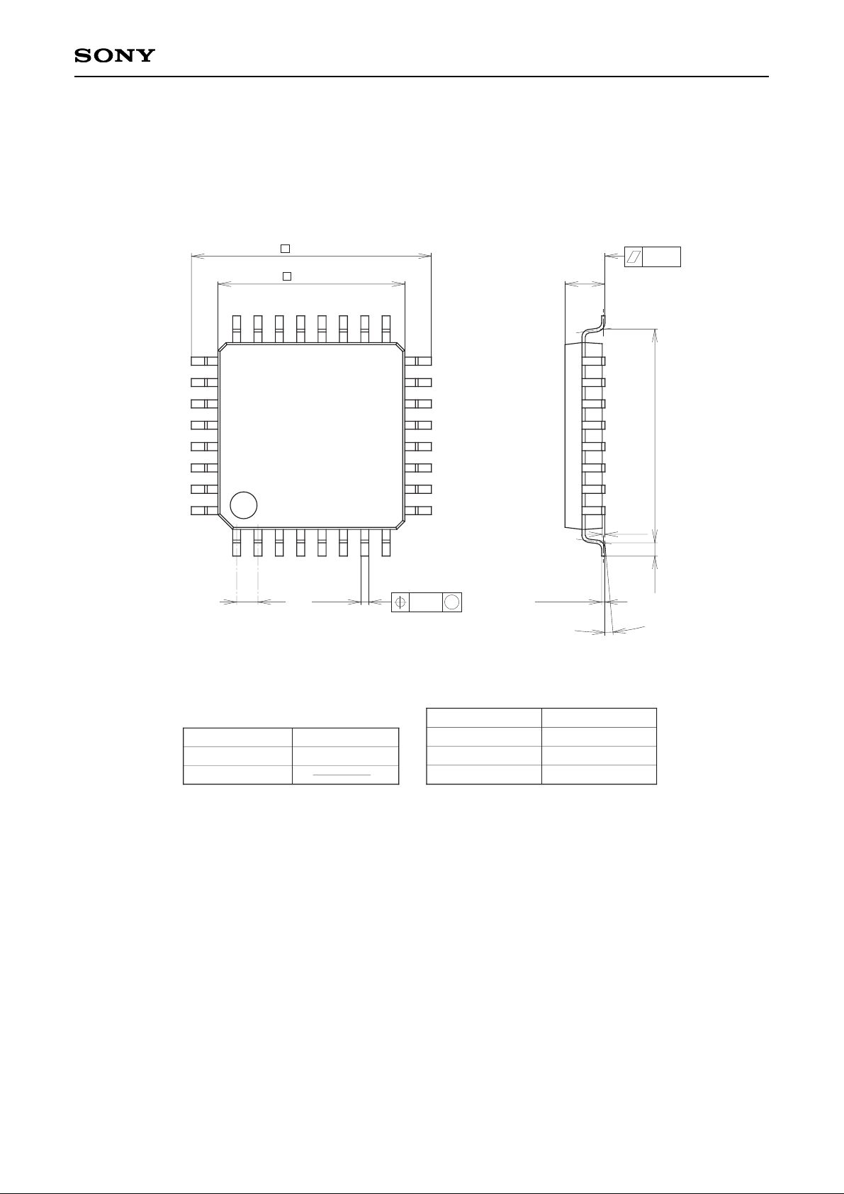
Package Outline Unit: mm
SONY CODE
EIAJ CODE
JEDEC CODE
PACKAGE MATERIAL
LEAD TREATMENT
LEAD MATERIAL
PACKAGE WEIGHT
EPOXY RESIN
SOLDER PLATING
42 ALLOY
32PIN QFP (PLASTIC)
9.0 ± 0.2
7.0 – 0.1
1.5 – 0.15
(8.0)
0.1 – 0.1
+ 0.2
+ 0.35
+ 0.3
0.50
0.127 – 0.05
+ 0.1
0° to 10°
0.8 0.3 – 0.1
+ 0.15
1
8
9
32
16
1724
25
M
± 0.12
0.1
0.2g
QFP-32P-L01
∗QFP032-P-0707-A
 Loading...