

Page 1
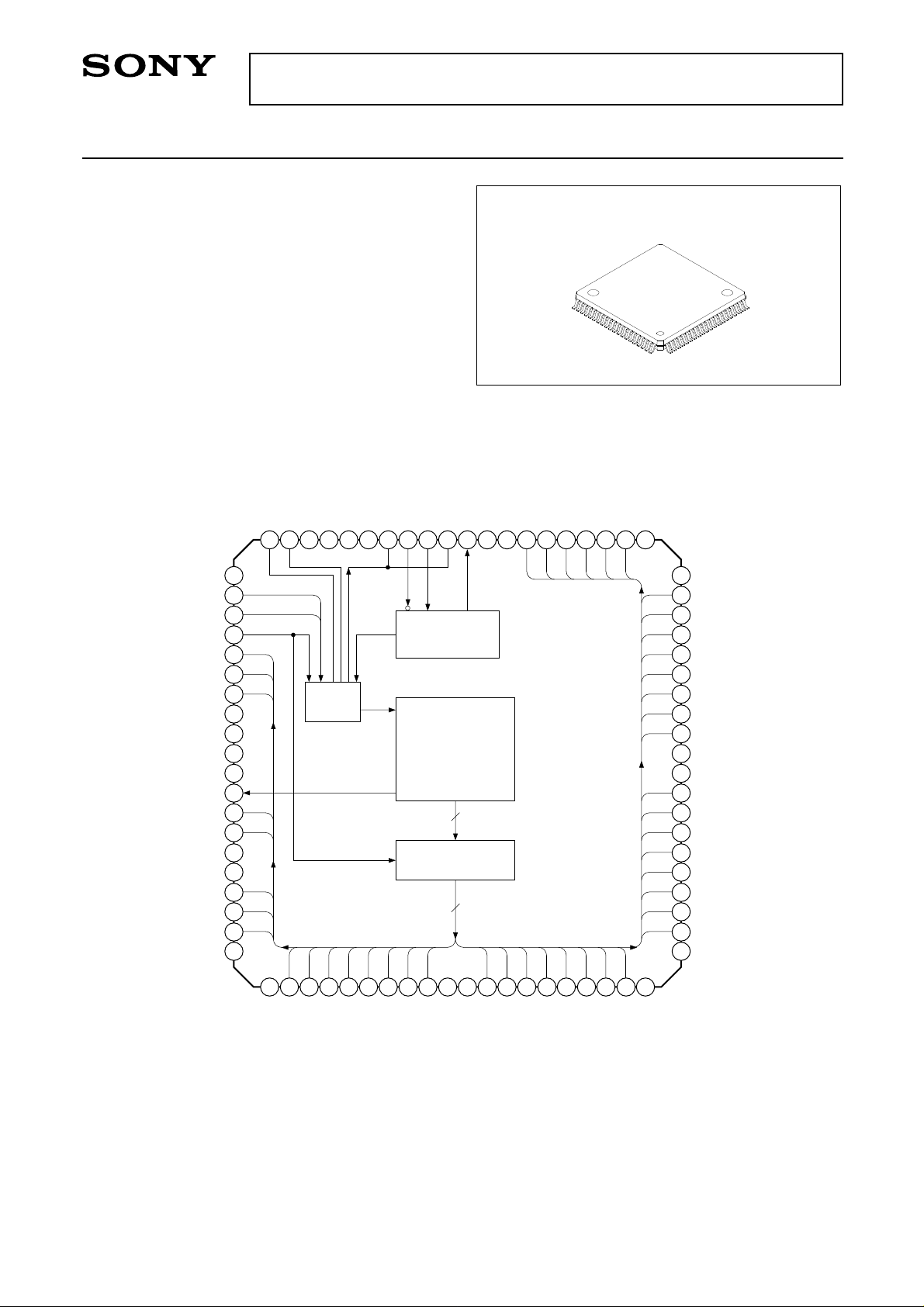
VGA/SVGA/XGA digital data serial receiver
Features
• 1 chip receiver for serial transmission of 18bit color
VGA/SVGA/XGA picture
• On chip differential cable driver
• TTL/CMOS compatible interface
• Support 1 pixel/shiftclock mode & 2 pixel/shiftclock
mode
• +3.3V single power supply
• Low power consumption
• 80pin Plastic QFP Package
(Body size: 14mm × 14mm)
Block Digagram & Pin out
LOS
49
T
T
CC
EE
V
V
RED0 (0)
46
48
47
60
LPFB
59
LPFA
58
A
A
S
CC
EE
EE
V
V
57
56
V
55
REFRQN
TESTSB
53
54
SDATAP
SDATAN
52
51
REFRQP
50
CXB1452Q
80 pin QFP (Plastic)
T
EE
RED0 (4)
RED0 (3)
RED0 (2)
RED0 (1)
45
44
43
RED0 (5)
41
42
V
TESTDT
PANEL1
PANEL0
CKMODE
CNTL3
CNTL2
CNTL1
V
EEG
CCG
V
CCT
V
EET
V
SFTCLK
HSYNC
VSYNC
EEG
V
CCG
V
CNTL0
BLU1 (5)
BLU1 (4)
CCT
V
61
62
63
64
65
66
67
68
69
70
71
72
73
74
75
76
77
78
79
80
1
T
EE
V
2
3
BLU1 (3)
CDR
PLL
4
BLU1 (1)
BLU1 (2)
6
5
BLU1 (0)
8
7
GRN1 (5)
GRN1 (4)
Cable
EQ
Serial
Parallell
Converter
Decoder
9
10
GRN1 (2)
GRN1 (3)
40
CCT
V
GRN0 (0)
39
38
GRN0 (1)
37
GRN0 (2)
36
GRN0 (3)
35
GRN0 (4)
GRN0 (5)
34
33
EEG
V
32
CCG
to
13
12
14
15
11
T
T
EE
CC
V
V
GRN1 (0)
GRN1 (1)
16
RED1 (4)
RED1 (5)
RED1 (3)
18
17
RED1 (2)
19
20
RED1 (0)
RED1 (1)
T
CC
V
31
30
29
28
27
26
25
24
23
22
21
V
EET
V
VCCT
BLU0 (0)
BLU0 (1)
BLU0 (2)
EEG
V
CCG
V
BLU0 (3)
BLU0 (4)
BLU0 (5)
EET
V
Fig. 1. Block Diagram & Pin out
Sony reserves the right to change products and specifications without prior notice. This information does not convey any license by
any implication or otherwise under any patents or other right. Application circuits shown, if any, are typical examples illustrating the
operation of the devices. Sony cannot assume responsibility for any problems arising out of the use of these circuits.
– 1 –
E97937-PS
Page 2

Pin List
Power/Ground
CXB1452Q
Pin Name
VCCT
VEET
VCCG
VEEG
VCCA
VEEA
VEES
Digital Signals
Pin Name
SFTCLK
RED1 (5 to 0)
GRN1 (5 to 0)
BLU1 (5 to 0)
RED0 (5 to 0)
GRN0 (5 to 0)
BLU0 (5 to 0)
Pin Number Descriptions
10, 20, 30, 40, 48, 70, 80
1, 11, 21, 31, 41, 49, 71
25, 32, 69, 76
26, 33, 68, 75
56
57
58
Pin Number Type Descriptions
72
14, 15, 16, 17, 18, 19
6, 7, 8, 9, 12, 13
78, 79, 2, 3, 4, 5
42, 43, 44, 45, 46, 47
34, 35, 36, 37, 38, 39
22, 23, 24, 27, 28, 29
TTL power surpply , should be connected to 3.3V ± 5%
TTL ground, connected to 0V
Logical core power surpply, connected to 3.3V ± 5%
Logical core ground, connected to 0V
Analog power surpply, connected to 3.3V ± 5%
Analog ground, connected to 0V
Analog substrate, connected to 0V
TTL out
TTL out
TTL out
Shift clock, for the data fetch at falling or rising edge
Pixel data input in 1 pixcel/sftclk mode
2nd pixel data input in 2 pixel/sftclk mode
High fixed in 1 pixcel/sftclk mode
1st pixel data input in 2 pixel/sftclk mode
HSYNC
VSYNC
CNTL (3 to 0)
PANEL (1, 0)
CKMODE
LOS
SDATAP/N
REFRQP/N
Special
Pin Name
TESTSB/DT
LPFA/B
73
74
65, 66, 67, 77
62, 63
64
50
52, 53
51, 54
TTL out
TTL out
TTL out
TTL in
TTL in
TTL out
Rx
Rx
Hsync data
Vsync data
Control data
Panel mode select switch
Clock mode select switch
Los of signal
Serial input
Refclk request
Pin Number Descriptions
55, 61
59, 60
Polarity control of SFTCLK & TEST under fablication
External loop filter
– 2 –
Page 3
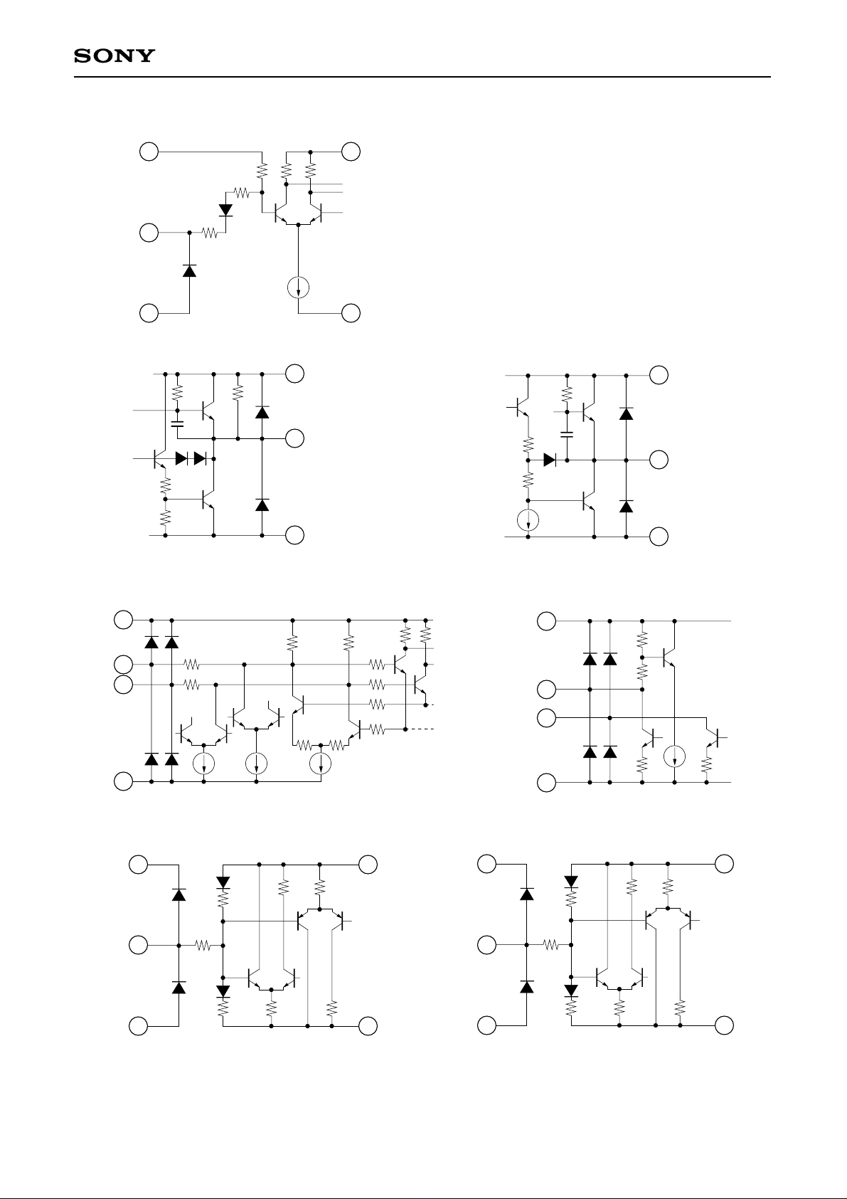
Equivalent I/O circuit
CXB1452Q
VCCT
6k
6k
TTL-IN
300
VEET
(a) TTL input equivalent circuit
3k
(b) TTL output equivalent circuit
SFTCLK, LOS
VCCT
TTL-OUT
V
EET
VCCG
V
EEG
VCCT
TTL-OUT
V
EET
(b') TTL output equivalent circuit
REDxx, GRNxx, BLUxx, H/V sync, CNTLx
VCCA
LPFA
LPFB
EEA
V
VCCA
TESTDT
EEA
V
VCCG
SDATAP/N
REFRQP/N
EEG
V
(c) LPFA/B equivalent circuit (d) SDATAP/N REFRQP/N equivalent circuit
V
V
CCG
EEG
VCCT
TESTSB
EETVEEG
V
V
CCG
(e) TESTDT equivalent circuit (f) TESTSB equivalent circuit
– 3 –
Page 4
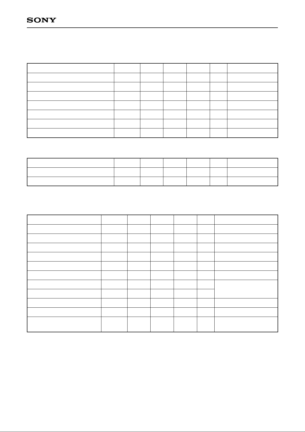
Electrical characteristics
Tab. 1. Absolute Maximum Rating
CXB1452Q
Description
Power supply voltage
TTL DC input voltage
TTL output current (High)
TTL output current (Low)
Serial output pin voltage
Ambient temperature
Storage temperature
Symbol Min. Typ. Max. Unit Comments
VCC
VI_T
IOH_T
IOL_T
Vsdout
Ta
Tstg
–0.3
–0.5
–20
0
–0.5
–55
–65
4
5.5
0
20
VCC + 0.5
60
150
Tab. 2. Recommended Operating Conditions
Description
Power supply voltage (Include VCCT5)
Ambient temperature
Symbol Min. Typ. Max. Unit Comments
VCC
Ta
3.135
0
3.3 3.465
60
Tab. 3. DC Characteristics (Under the recommended conditons. See Tab. 2)
V
V
mA
'
mA
V
°C°CUnder bias
V
°C
Description
Input HIGH voltage (TTL)
Input LOW voltage (TTL)
Input HIGH current (TTL)
Input LOW current (TTL)
Output HIGH voltage (TTL)
Output LOW voltage (TTL)
Output HIGH current (REFREQ)
Output LOW current (REFREQ)
Input dynamic range (SDATA)
Input dynamic range (SDATA)
Supply current
Symbol Min. Typ. Max. Unit Conditions
VIH_T
VIL_T
IIH_T
IIL_T
VOH_T
VOL_T
IOH_RQ
2
–0.5
–400
2.25
–0.1
5.5
0.8
20
0.4
0
+0.1
V
V
µA
µA
V
V
mA
VIN = VCC
VIN = 0
IOH = –0.2mA
IOL = 4mA
See Fig. 2
IOL_RQ
VIM_SD
VID_SD
ICC
7.4
VCC – 0.4
–0.5
230
220
8.0
310
300
8.6
VCC + 0.2
+0.5
390
380
mA
V
V
mA
mA
Common mode voltage
Differential voltage
2 pixel/sftclk, Outputs open
1 pixel/sftclk, Outputs open
– 4 –
Page 5
CXB1452Q
VCC
61
55
VCCA/G/T
CXB1452Q
V
EEA/G/T
51
54
A
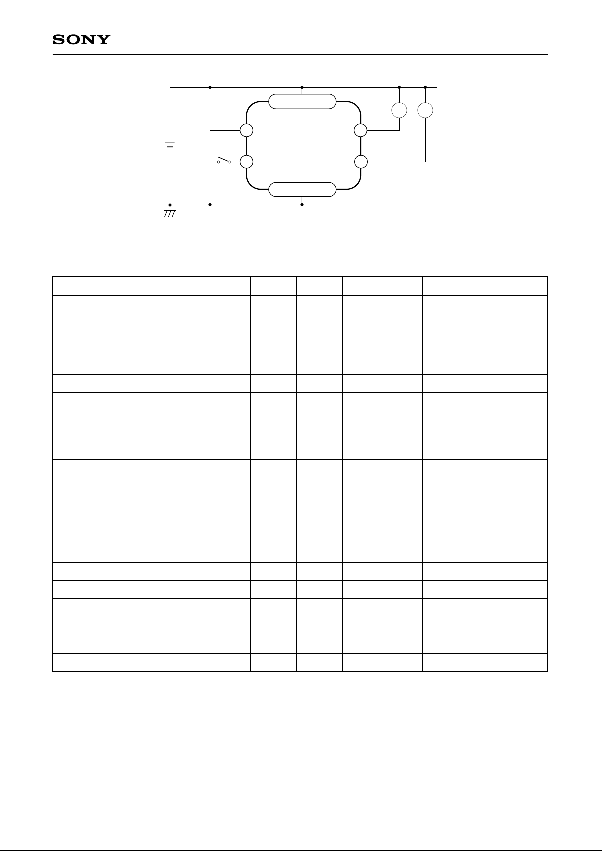
Fig. 2. IOH_RQ and IOL_RQ DC measurement
Tab. 4. AC Characteristics (Under the recommended conditons. See Tab. 5)
Description
SFTCLK frequency
SFTCLK duty factor
Symbol Min. Typ. Max. Unit Conditions
Fsftclk
Dsftclk
20.0
10.0
38.0
19.0
60.0
30.0
35
25.0
12.5
40.0
20.0
65.0
32.5
28.0
14.0
48.0
24.0
68.0
34.0
65
MHz
MHz
MHz
MHz
MHz
MHz
%
A
VGA, 1 pixel/sftclk mode
VGA, 2 pixel/sftclk mode
SVGA, 1 pixel/sftclk mode
SVGA, 2 pixel/sftclk mode
XGA, 1 pixel/sftclk mode
XGA, 2 pixel/sftclk mode
Vth = 1.4V, CL = 10pF
Pixel/Sync/Cntl setup to
SFTCLK
Pixel/Sync/Cntl hold to
SFTCLK
SFTCLK rise time
SFTCLK fall time
Pixel/Sync/Cntl rise time
Pixel/Sync/Cntl fall time
CLOCK mode assert time
CLOCK mode deassert time
LOS signal assert time
LOS signal deassert time
Tsetup
Thold
Torc
Tofc
Tord
Tord
TAclk
TDclk
TAlos
TDlos
24.0
11.0
3.5
20.0
6.5
4.0
2.5
1.0
0.9
50
0.8
0.1
4.0
3.0
7.0
6.0
Vth = 1.4V, CL = 10pF
ns
VGA, 1 pixel/sftclk 25MHz
ns
SVGA, 1 pixel/sftclk 40MHz
ns
XGA, 1 pixel/sftclk 65MHz
ns
XGA, 2 pixel/sftclk 32.5MHz
Vth = 1.4V, CL = 10pF
ns
VGA, 1 pixel/sftclk 25MHz
ns
SVGA, 1 pixel/sftclk 40MHz
ns
XGA, 1 pixel/sftclk 65MHz
ns
XGA, 2 pixel/sftclk 32.5MHz
ns
0.8V to 2.0V, CL = 10pF
ns
2.0V to 0.8V, CL = 10pF
ns
0.8V to 2.0V, CL = 10pF
ns
2.0V to 0.8V, CL = 10pF
µs
µs
µs
µs
– 5 –
Page 6
VCC
VCCA/G/T
TTLout
CXB1452Q
CL'
V
EEA/G/T
CL' + Cprobe = 10pF
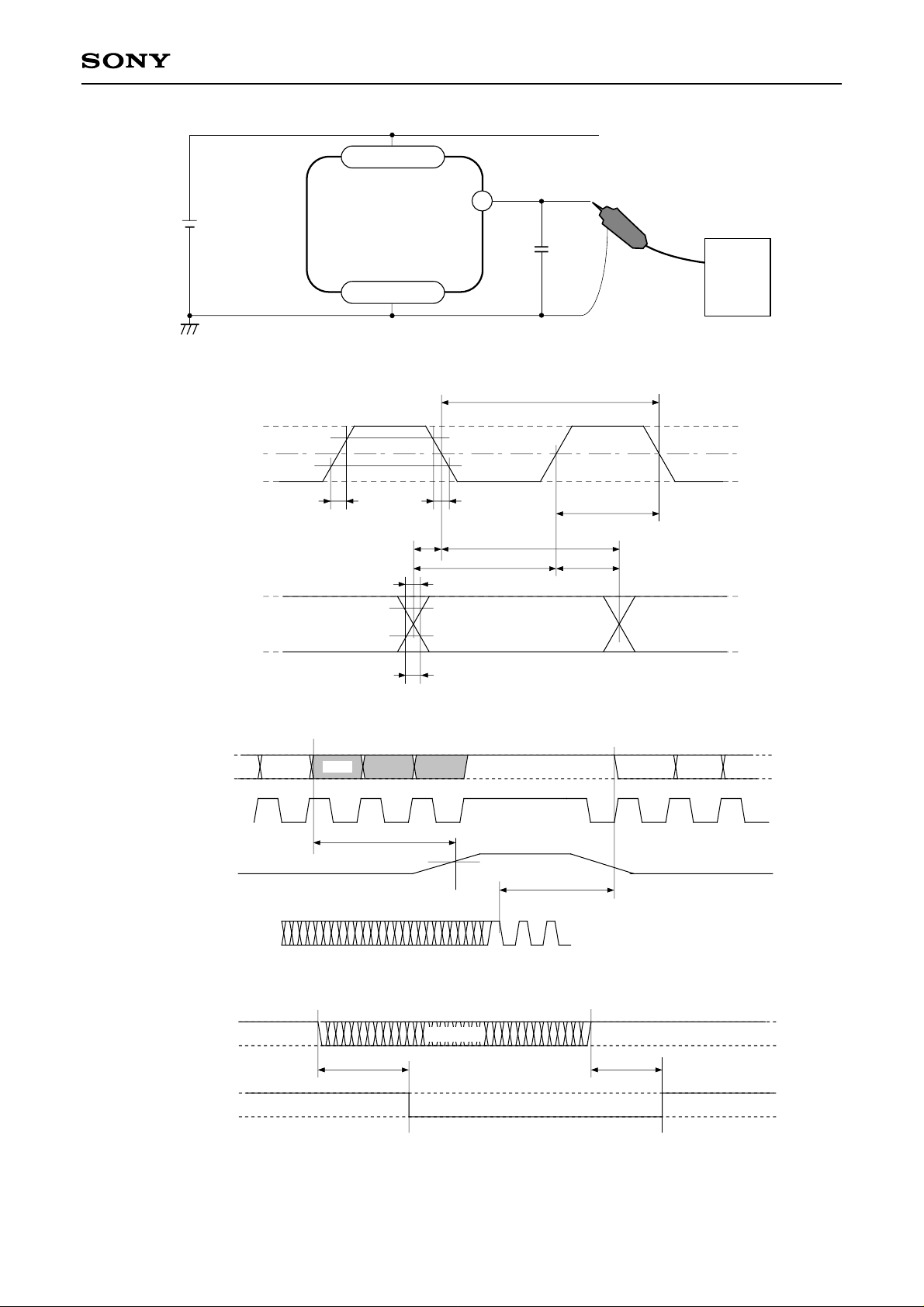
Fig. 3. SDATA waveform measurement
CXB1452Q
Cprobe
oscilloscope
Timing Chart
SFTCLK
Setup/hold time is refered from
rise edge in TESTSB/DT = GND or OPEN
fall edge in TESTSB/DT = V CC
REDxx
GRNxx
BLUxx
H/Vsync
CNTLx
Pixel
Sync/Cntl
SftClk
REFRQP
REFRQN
Torc
Tsetup
Tord
2.0V
0.8V
Tofd
Fig. 4. TTL output timing
error
TAclk
1/Fsftclk
2.0V
Vth
0.8V
Tofc
Dsftclk/Fsftclk
Thold
TDclk
SDATAP
SDATAN
SDATAP
SDATAN
LOS
Fig. 5. Refclk request timing
NRZ data
TDlos TAlos
Fig. 6. Idle mode timing
– 6 –
Page 7
CXB1452Q
Operation mode
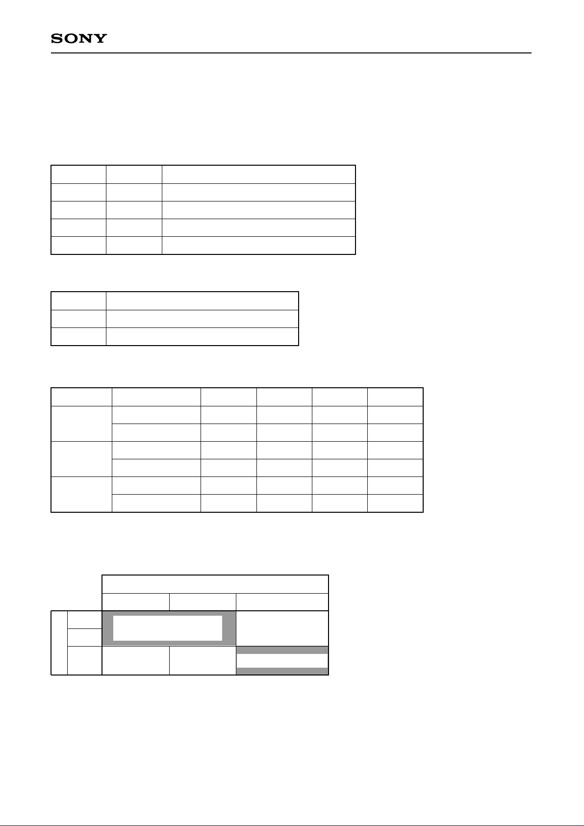
CXB1452Q supports 3 panel mode and 2 clock mode switched by the PANEL (1, 0) and CKMODE pin
according to the Tab. 5 & 6. The supporting color depth and clock rate are summarized in Tab. 7. These pins
are open High TTL inputs.
Tab. 5. Panel Mode select
PANEL1
L
L
H
H
PANEL0 Supporting panel size & color
L
H
L
H
Tab. 6. Clock Mode select
CKMODE
L
H
2 pixel/ShiftClock (2ppc)
1 pixel/ShiftClock (1ppc)
Supporting clock mode
Tab. 7. Operation Mode
Panel Mode
Clock Mode Color Shift Clock Dot Clock Serial rate
1 pixel/SftClk
VGA
2 pixel/SftClk
1 pixel/SftClk
SVGA
2 pixel/SftClk
VGA (640 × 480) 18bit color
SVGA (800 × 600) 18bit color
XGA (1024 × 768) 18bit color
not supported
18bit
18bit
18bit
18bit
25MHz
12.5MHz
40MHz
20MHz
25MHz
25MHz
40MHz
40MHz
600Mbps
600Mbps
960Mbps
960Mbps
1 pixel/SftClk
18bit
65MHz
65MHz
1560Mbps
XGA
2 pixel/SftClk
18bit
32.5MHz
65MHz
1560Mbps
TESTSB/TESTDT pins select the trigger edge of SFTCLK and test mode according to Tab. 8.
Tab. 8. SFTCLK polarity & TEST mode
TESTSB
GND
OPEN
TESTDT
VCC
GND
Receiver operation
trigger = rising edge
All TTL out
= Low
OPEN VCC
Fabricator reserved
TEST mode
All TTL out
= High
Trigger = falling edge
LOS pin shows the absence of proper level of SDATA signal. LOS pin is High when connector is disconnected
or transmitter is idle.
– 7 –
Page 8
Applications
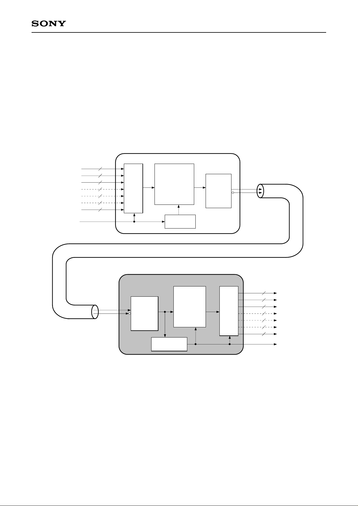
CXB1452Q GVIF receiver is applied to the digital RGB signal transmittion for
P/C with LCD monitor
Video on demand system
Monitoring system
Graphical controller
Projector
Digital TV monitor
with GVIF transmitter, CXB1451Q.
CXB1451Q GVIF Transmitter
CXB1452Q
RED1 (5 to 0)
GRN1 (5 to 0)
BLU1 (5 to 0)
RED0 (5 to 0)
GRN0 (5 to 0)
BLU0 (5 to 0)
SYNC/CNTL
SHIFTCLOCK
RED0/GRN0/BLU0
are active in 2pixel/shiftclock
mode only
6
6
6
6
6
6
6
Encoder
Cable
Equalizer
Parallel
to
Serial
Converter
PLL
STP or Twin axial
Serial
to
Parallel
Converter
PLL
Cable
Driver
Decoder
6
6
6
6
6
6
6
RED1 (5 to 0)
GRN1 (5 to 0)
BLU1 (5 to 0)
RED0 (5 to 0)
GRN0 (5 to 0)
BLU0 (5 to 0)
SYNC/CNTL
SHIFTCLOCK
CXB1452Q GVIF Receiver
– 8 –
Page 9
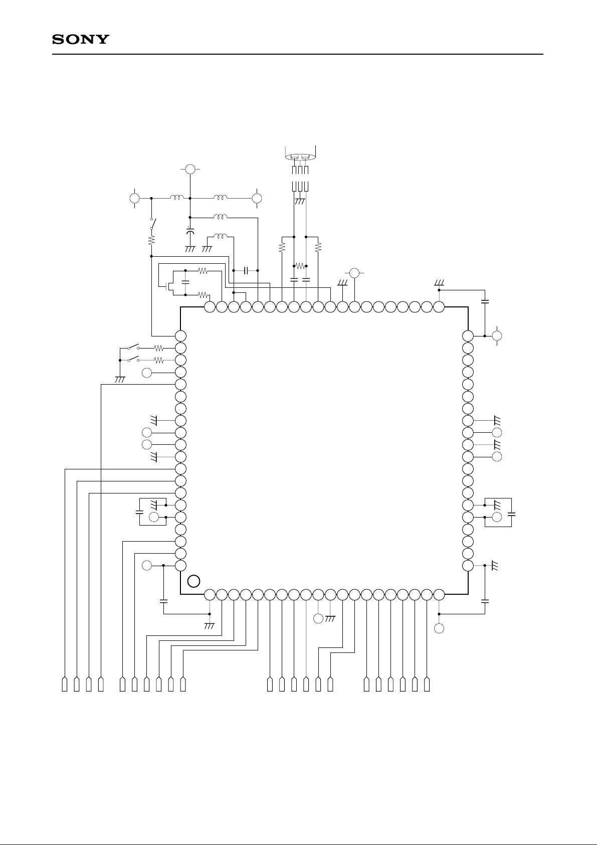
Application Cicuit (A)
Clock mode: 1 pixel/sftclk (1ppc)
Picture sync: H/V sync & DE
Color depth: 18bit
CXB1452Q
Differential cable
VCC
Select SFTCLK polarity
according to Tab. 8
Rf = 470 (XGA/SVGA)
= 150 (VGA)
2SK303
Select panel resolution
according to Tab. 5
SW2
SW3
0.1µ
(2)
E
SW0
(4)
T
E
T
T
0.1µ
330
330
E
(2)
0.1 to 0.4n
(3)
33µ
16V
1k
S
100p (2)
61
62
63
64
65
66
67
68
69
70
71
72
73
74
75
76
77
78
79
80
0.1 to 0.4n (3)
0.1 to 0.4n (3)
0.1 to 0.4n (3)
Rf (1)
Rf (1)
60
TESTDT
PANEL1
PANEL0
CKMODE
CNTL3
CNTL2
CNTL1
EEG
V
CCG
V
CCT
V
EET
V
SFTCLK
HSYNC
VSYNC
EEG
V
CCG
V
CNTL0
BLU1 (5)
BLU1 (4)
CCT
V
1
59
LPFB
T
EE
V
2
0.1µ
(2)
57
58
S
EE
V
LPFA
BLU1 (3)
BLU1 (2)
3
T
56
A
EE
V
BLU1 (1)
5
4
150
(1)
47p
(1)
55
54
A
CC
V
TESTSB
GRN1 (5)
BLU1 (0)
6
Connector
53
SDATAN
REFRQN
GRN1 (3)
GRN1 (4)
8
7
100 (1)
52
51
SDATAP
GRN1 (2)
9
10
150
(1)
47p
(1)
50
LOS
REFRQP
T
T
EE
CC
V
V
11
T
T
49
48
T
EE
V
GRN1 (1)
13
12
(1) CHIP RESISTOR (1%)
(2) CHIP CAPACITOR
(3) FORMED BY THE PRINTED CIRCUIT PATTERN
(L = 0.5 to 1.0mm/W = 0.5 to 1.0mm)
(4) Idss rank 3mA
46
47
T
CC
V
RED0 (0)
GRN1 (0)
RED1 (5)
14
15
45
44
RED0 (1)
RED0 (2)
RED1 (3)
RED1 (4)
17
16
43
RED0 (4)
RED0 (3)
RED1 (1)
RED1 (2)
19
18
4142
T
EE
V
CCT
V
RED0 (5)
GRN0 (0)
GRN0 (1)
GRN0 (2)
GRN0 (3)
GRN0 (4)
GRN0 (5)
EEG
V
CCG
V
EET
V
VCCT
BLU0 (0)
BLU0 (1)
BLU0 (2)
EEG
V
CCG
V
BLU0 (3)
BLU0 (4)
BLU0 (5)
EET
V
T
CC
RED1 (0)
V
20
0.1µ
40
39
38
37
36
35
34
33
32
31
30
29
28
27
26
25
24
23
22
21
0.1µ
T
(2)
(2)
T
E
T
0.1µ
E
(2)
HSYNC
SFTCLK
543210
DE
MSB LSB
VSYNC
BLUE DATA
543210
MSB LSB
GREEN DATA
543210
MSB LSB
RED DATA
Application circuits shown are typical examples illustrating the operation of the devices. Sony cannot assume responsibility for
any problems arising out of the use of these circuits or for any infringement of third party patent and other right due to same.
– 9 –
Page 10
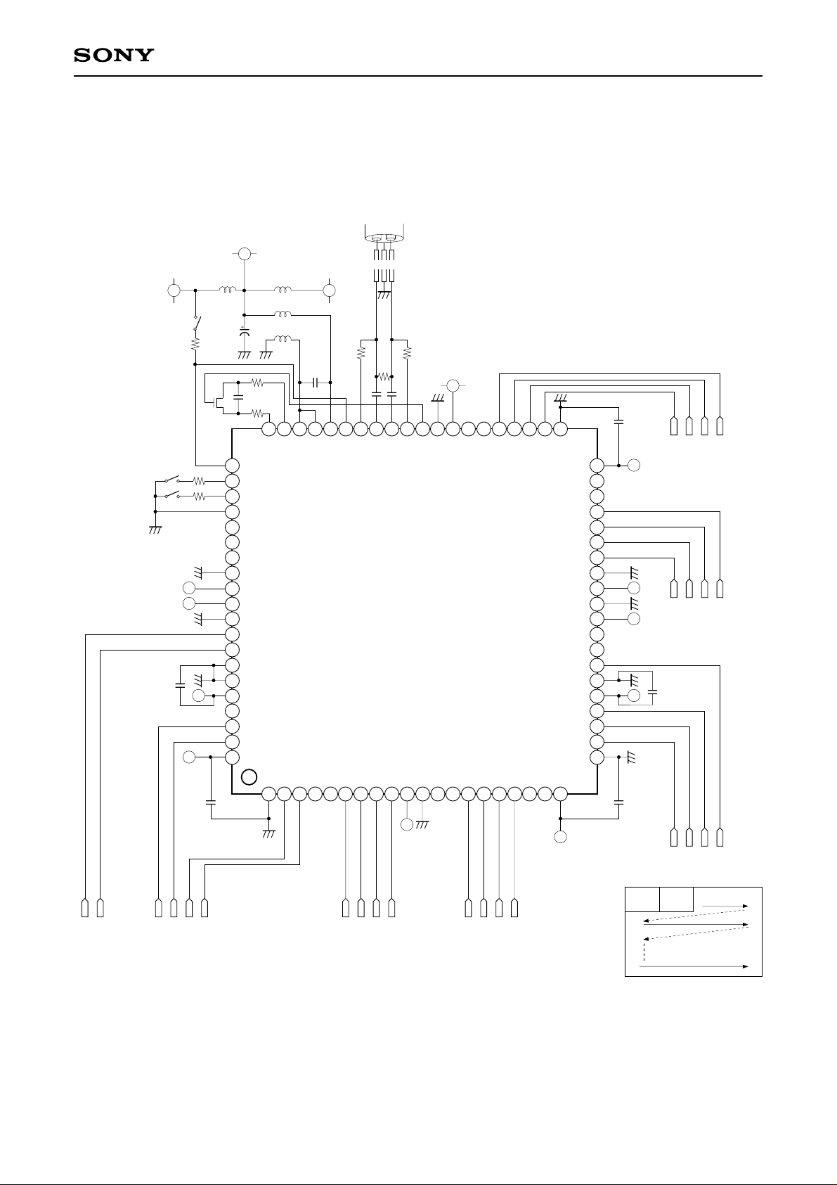
Application Cicuit (B)
Clock mode: 2 pixel/sftclk
Picture sync: ENABLE only
Color depth: 12bit
CXB1452Q
Differential cable
VCC
Select SFTCLK polarity
according to Tab. 8
Rf = 470 (XGA/SVGA)
= 150 (VGA)
2SK303
Select panel resolution
according to Tab. 5
0.1µ
(2)
3210
MSB LSB
ENABLE
EVEN BLUE DATA
SFTCLK
E
(4)
SW2
SW3
SW0
0.1 to 0.4n
1k
330
330
E
T
E
T
0.1µ
(2)
(3)
33µ
16V
S
100p (2)
61
62
63
64
65
66
67
68
69
70
71
72
73
74
75
76
77
78
79
80
0.1 to 0.4n (3)
0.1 to 0.4n (3)
0.1 to 0.4n (3)
Rf (1)
Rf (1)
60
TESTDT
PANEL1
PANEL0
CKMODE
CNTL3
CNTL2
CNTL1
EEG
V
CCG
V
CCT
V
EET
V
SFTCLK
HSYNC
VSYNC
EEG
V
CCG
V
CNTL0
BLU1 (5)
BLU1 (4)
CCT
V
1
59
LPFB
T
EE
V
58
LPFA
BLU1 (3)
2
3
T
150
(1)
0.1µ
(2)
47p
(1)
55
57
56
A
A
S
EE
EE
CC
V
V
V
TESTSB
BLU1 (0)
BLU1 (1)
BLU1 (2)
GRN1 (5)
6
5
4
3210
MSB LSB
EVEN GREEN DATA
Connector
53
54
REFRQN
GRN1 (4)
8
7
100 (1)
52
51
SDATAP
SDATAN
GRN1 (2)
GRN1 (3)
9
10
T
150
(1)
47p
(1)
49
50
LOS
REFRQP
T
T
CC
EE
V
V
12
11
T
46
48
T
EE
V
GRN1 (1)
13
45
47
T
CC
V
RED0 (1)
RED0 (0)
RED1 (4)
RED1 (5)
GRN1 (0)
14
15
16
3210
MSB LSB
EVEN RED DATA
(1) CHIP RESISTOR (1%)
(2) CHIP CAPACITOR
(3) FORMED BY THE PRINTED CIRCUIT PATTERN
(L = 0.5 to 1.0mm/W = 0.5 to 1.0mm)
(4) Idss rank 3mA
0.1µ
43
44
RED0 (3)
RED0 (2)
RED1 (3)
RED1 (2)
18
17
41
42
RED0 (4)
RED0 (5)
GRN0 (0)
GRN0 (1)
GRN0 (2)
GRN0 (3)
GRN0 (4)
GRN0 (5)
BLU0 (0)
BLU0 (1)
BLU0 (2)
BLU0 (3)
BLU0 (4)
BLU0 (5)
RED1 (0)
RED1 (1)
19
20
T
EE
V
V
V
V
V
VCCT
V
V
V
T
CC
V
CCT
EEG
CCG
EET
EEG
CCG
EET
(2)
MSB LSB
T
ODD RED DATA
40
39
38
37
36
35
34
33
E
32
31
30
29
MSB LSB
T
ODD GREEN DATA
28
27
26
25
0.1µ
E
(2)
24
23
22
21
0.1µ
(2)
T
MSB LSB
ODD BLUE DATA
ODD
EVEN
PIXEL
PIXEL
Transmission order
of the PIXEL
3210
3210
3210
Application circuits shown are typical examples illustrating the operation of the devices. Sony cannot assume responsibility for
any problems arising out of the use of these circuits or for any infringement of third party patent and other right due to same.
– 10 –
Page 11
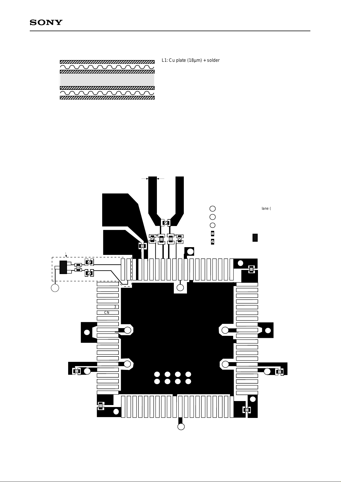
Recommended Printed Circuit Board Structure
L1:Cu plate (18µm) + solder coat
I1: Adhesive Sheet (0.3mm ± 0.09mm)
L2:Cu plate (36µm)
I2: Fiber-glass epoxy core (0.8mm)
L3:Cu plate (36µm)
I3: Adhesive Sheet (0.3mm)
L4:Cu plate (18µm) + solder coat
Recommended Printed Circuit Board Pattern
SDATAP/SDATAN pins to the connector path W = 0.50mm (Z0 = 50Ω)
other path W = 0.25mm
POWER and special signal routing example
0.5mm
CXB1452Q
L2 doesn't have plane
in this area
To LOS
Through hole to the GND plane (L2)
G
Through hole to the V
E
Through hole to the V
T
Chip capacitor
Chip resistor
G
41
60
REFRQP
LOS
T
T
CC
EE
V
V
RED0 (1)
RED0 (0)
RED0 (2)
RED0 (3)
RED0 (4)
T
EE
RED0 (5)
V
A
A
S
EE
EE
CC
LPFA
V
TESTSB
LPFB
V
61
TESTDT
SDATAN
V
REFRQN
SDATAP
PANEL1
PANEL0
CKMODE
CNTL3
CNTL2
CNTL1
V
EEG
V
G
CCG
V
V
CCT
EET
E
E
SFTCLK
HSYNC
VSYNC
V
EEG
V
G
E
CCG
CNTL0
BLU1 (5)
T TTT
TTTT
G
BLU1 (4)
V
CCT
GRN1 (3)
GRN1 (2)
T
CC
V
T
EE
V
GRN1 (1)
GRN1 (0)
RED1 (5)
RED1 (4)
RED1 (3)
T
EE
V
G
BLU1 (3)
BLU1 (1)
BLU1 (2)
BLU1 (0)
GRN1 (5)
GRN1 (4)
RED1 (1)
RED1 (2)
T
CC
V
RED1 (0)
CCE/VCCG plane (L3)
CCT plane (L3)
G
VCCT
GRN0 (0)
GRN0 (1)
GRN0 (2)
GRN0 (3)
GRN0 (4)
GRN0 (5)
EEG
V
V
CCG
EET
V
V
CCT
BLU0 (0)
BLU0 (1)
BLU0 (2)
V
EEG
CCG
V
BLU0 (3)
BLU0 (4)
BLU0 (5)
V
EET
G
FET
40
G
E
2180
201
G
– 11 –
Page 12
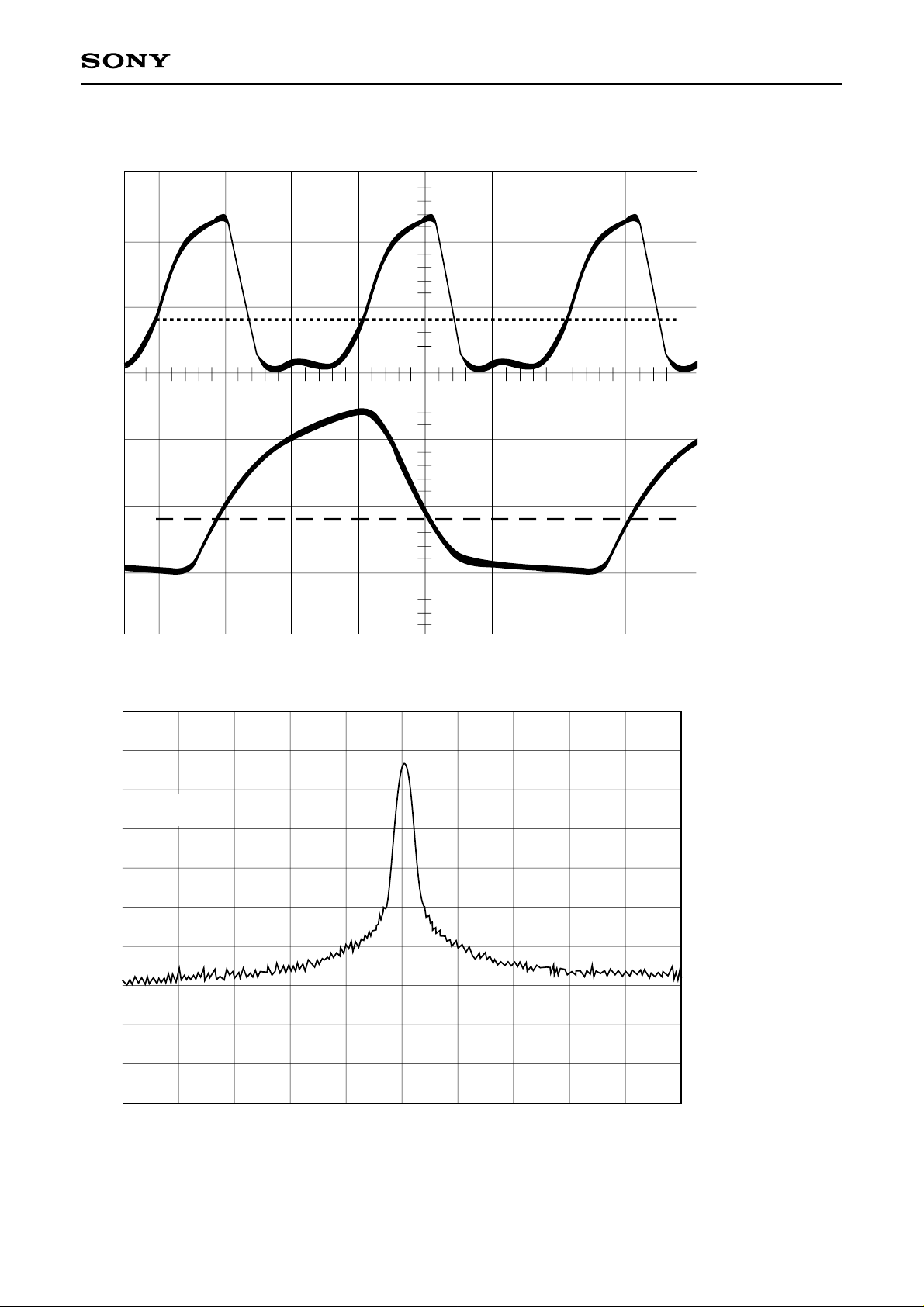
TTL output waveform with CL = 10pF
CXB1452Q
SFTCLK
65MHz
TTL output
B15
65Mb/s
TTL output
D
1V 1V 5ns
SFTCLK Power spectrum
REF LVL
0dBm
ATTEN 10dB
RL 0dBm
10dB/
SFTCLK
32.5MHz
CENTER 32.50MHz
RBW 100kHz
VBW 100kHz
SPAN 10.00MHz
SWP 50.0ms
– 12 –
Page 13
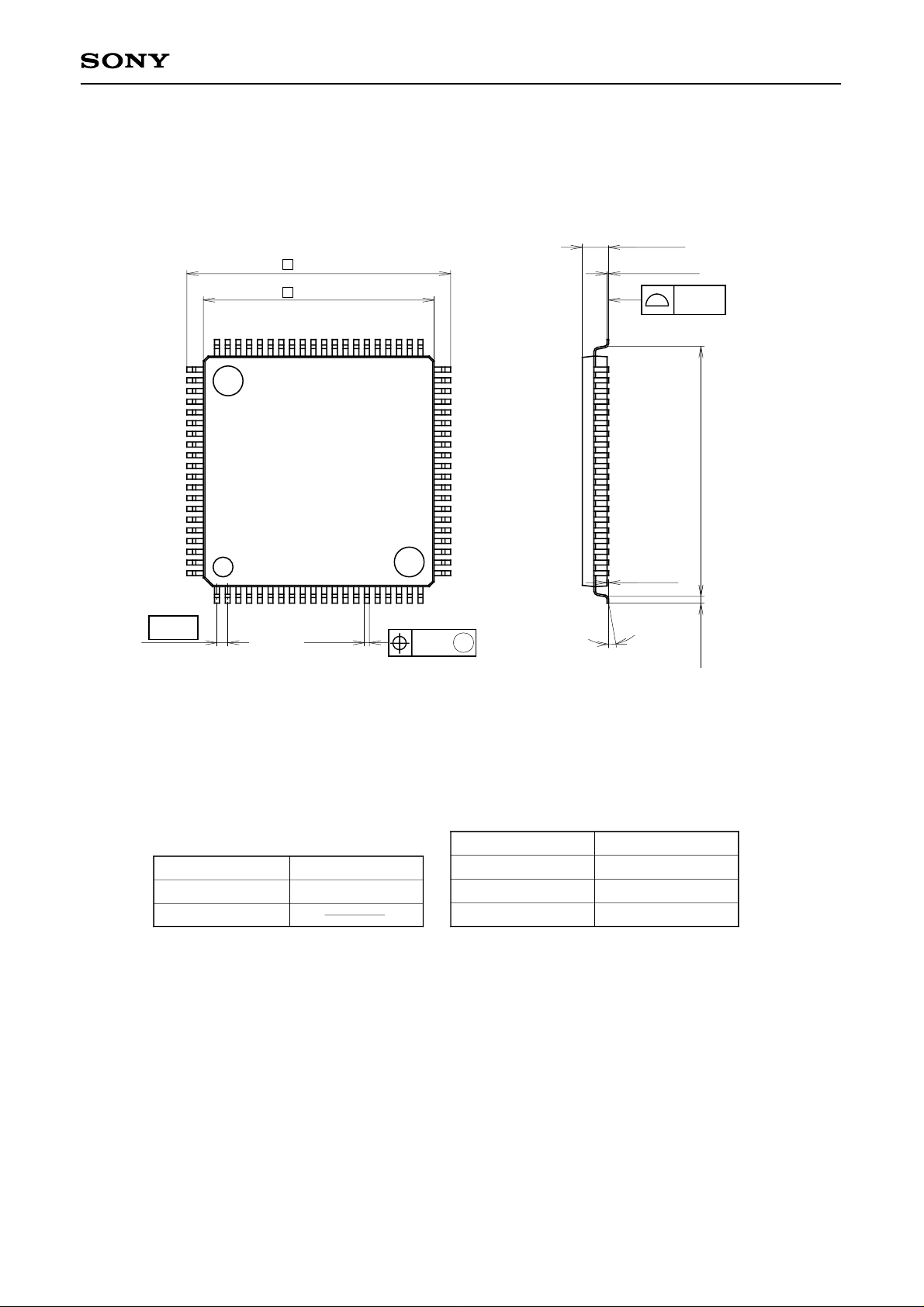
Package Outline Unit: mm
16.0 ± 0.4
14.0 – 0.1
+ 0.4
80PIN QFP (PLASTIC)
+ 0.35
1.5 – 0.15
+ 0.1
0.127 – 0.05
CXB1452Q
0.1
61
80
0.65
60
41
40
(15.0)
21
1
+ 0.15
0.3 – 0.1
20
0.24
M
0.1 – 0.1
0° to 10°
+ 0.15
0.5 ± 0.2
SONY CODE
EIAJ CODE
JEDEC CODE
QFP-80P-L03
QFP080-P-1414
PACKAGE STRUCTURE
PACKAGE MATERIAL
LEAD TREATMENT
LEAD MATERIAL
PACKAGE MASS
– 13 –
EPOXY RESIN
SOLDER PLATING
42/COPPER ALLOY
0.6g
 Loading...